

ViewSonic VE710b-4, VE710s-4, VS10047 Service Manual

ViewSonic VE710b-4
VE710s-4
Model No. VS10047
17” Color TFT LCD Display
(VE710s-4_VE710b-4_SM Rev. 1a Jun. 2006)
ViewSonic 381 Brea Canyon Road, Walnut, California 91789 USA – (800) 888 -8583
Service Manual
ViewSonic Corporation Confidential - Do Not Copy VE710s-4_VE710b-4
i
Copyright
Copyright © 2006 by ViewSonic Corporation. All rights reserved. No part of this publication
may be reproduced, transmitted, transcribed, stored in a retrieval system, or translated into any
language or computer language, in any form or by any means, electronic, mechanical, magnetic,
optical, chemical, manual or otherwise, without the prior written permission of ViewSonic
Corporation.
Disclaimer
ViewSonic makes no representations or warranties, either expressed or implied, with respect to
the contents hereof and specifically disclaims any warranty of merchantability or fitness for any
particular purpose. Further, ViewSonic reserves the right to revise this publication and to make
changes from time to time in the contents hereof without obligation of ViewSonic to notify any
person of such revision or changes.
Trademarks
Opt quest is a registered trademark of ViewSonic Corporation.
ViewSonic is a registered trademark of ViewSonic Corporation.
All other trademarks used within this document are the property of their respective owners.
Revision History
Revision SM Editing Date ECR Number Description of Changes Editor
1a 06/27/2006 Initial Release J. Chang
ViewSonic Corporation Confidential - Do Not Copy VE710s-4_VE710b-4
ii
TABLE OF CONTENTS
1. Precautions and Safety Notices 1
2. Specification 2
3. Front Panel Function Control Description 4
4. Circuit Description 11
5. Adjustment Procedure 19
6. Troubleshooting Flow Chart 39
7. Recommended Spare Parts List 43
8. Exploded Diagram and Exploded Parts List 63
9. Block Diagram 68
10. Schematic Diagrams 71
11. PCB Layout Diagrams 81

1. Precautions and Safety Notices (VE710s-4/VE710b-4)
1.1. SAFETY PRECAUTIONS
This monitor is manufactured and tested on a ground principle that a user's safety comes first. However,
improper use or installation may cause damage to the monitor as well as to the user. Carefully go over the
following WARNINGS before installing and keep this guide handy.
WARNINGS:
u This monitor should be operated only at the correct power sources indicated on the label on the rear end of
the monitor. If you're unsure of the power supply in your residence, consult your local dealer or power
company.
u Use only the special power adapter that comes with this monitor for power input.
u Do not try to repair the monitor your self as it contains no user -serviceable parts. This monitor should only
be repaired by a qualified technician.
u Do not remove the monitor cabinet. There is high-voltage parts inside that may cause electric shock to
human bodies, even when the power cord is unplugged.
u Stop using the monitor if the cabinet is damaged. Have it checked by a service technacian.
u Put your monitor only in a clean, dry environment. If it gets wet, unplug the power cable immediately and
consult your service technician.
u Always unplug the monitor before cleaning it. Clean the cabinet with a clean, dry cloth. Apply
non-ammonia based cleaner onto the cloth, not directly onto the glass screen.
u Keep the monitor away from magnetic objects, motors, TV sets, and transformer.
u Do not place heavy objects on the monitor or power cord.
1.2. PRODUCT SAFETY NOTICE
Many electrical and mechanical parts in this chassis have special safety visual inspections and the protection
afforded by them cannot necessarily be obtained by using replacement components rated for higher voltages,
wattage, etc. Before replacing any of these components read the parts list in this manual carefully. The use of
substitute replacement parts which do not have the same safety characteristics as specified in the parts list may
create shock, fire, or other hazards.
1.3. SERVICE NOTES
1. When replacing parts or circuit boards, clamp the lead wires around terminals before soldering.
2. When replacing a high wattage resistor (more than 1W of metal oxide film resistor) in circuit board, keep the
resistor about 5mm away from circuit board.
3. Keep wires away from high voltage, high temperature components and sharp edges.
4. Keep wires in their original position so as to reduce interference.
5. Usage of this product please refer to also user's manual.
ViewSonic Corporation Confidential - Do Not Copy VE710s-4_VE710b-4
1

2. Specification (VE710s-4/VE710b-4)
2.1. PRODUCT SPECIFICATIONS
LCD Panel 17.0" TFT
Power Management Energy Star compliant VESA
DPMS compatible
< 1W
Displayable Resolution SXGA 1280× 1024 (max.)
Pixel Dimension 0.264(H)× 0.264(V)mm
LCD Display Color 262K Color. (6bit)
Viewing Angle CR≧10
Horizontal: 140 deg
Vertical: 130 deg
Contrast Ratio 450 : 1 (typ.) 360:1 (min.)
Brightness 230 cd/ m2 (min.)
300 cd/m2 (typ.)
Response Time CPT Panel:
CLAA170EA08Q (8ms) Tr: 2 ms Tf: 6 ms (typ.) Tr: 7 ms Tf: 11 ms (max.)
CMO Panel:
M170E5-L09 (8ms) Tr: 2 ms Tf: 6 ms (typ.), Tr: 7 ms Tf: 11 ms (max.)
Active Display Area 337.9mm(H)× 270.3mm(V)
Temperature Operating: 0°C ~ +40°C
Storage: -20°C ~ +60°C
Compliance UL, CUL, TÜV, CE, FCC, VCCI, BSMI,CCC, Energy Star.
Power Input Voltage: 100~240 Vac
Consumption: 35 Watts (Max.)
2.2. FACTORY SUPPORTING MODES
Primary Preset: VESA 1280 x 1024 @ 60Hz
Look up table timing: 1. 640 x 350 @ 70Hz, 31.5kHz
2. 640 x 480 @ 60Hz, 31.5kHz
3. 640 x 480 @ 67Hz, 35.0kHz
4. 640 x 480 @ 75Hz, 37.5kHz
5. 640 x 480 @ 72Hz, 37.9kHz
6. 640 x 480 @ 85Hz, 43.27kHz
7. 720 x 400 @ 70Hz, 31.5kHz
8. 800 x 600 @ 56Hz, 35.1kHz
9. 800 x 600 @ 60Hz, 37.9kHz
ViewSonic Corporation Confidential - Do Not Copy VE710s-4_VE710b-4
2
10. 800 x 600 @ 75Hz, 46.9kHz
11. 800 x 600 @ 72Hz, 48.1kHz
12. 800 x 600 @ 85Hz, 53.7kHz
13. 832 x 624 @ 75Hz, 49.7kHz
14. 1024 x 768 @ 60Hz, 48.4kHz
15. 1024 x 768 @ 70Hz, 56.5kHz
16. 1024 x 768 @ 72Hz, 58.1kHz
17. 1024 x 768 @ 75Hz, 60.0kHz
18. 1024 x 768 @ 85Hz, 68.67kHz
19. 1280 x 1024 @ 60Hz, 63.4kHz
20. 1280 x 1024 @ 75Hz, 79.97kHz
21. 1280x720 @ 60Hz, 45kHz
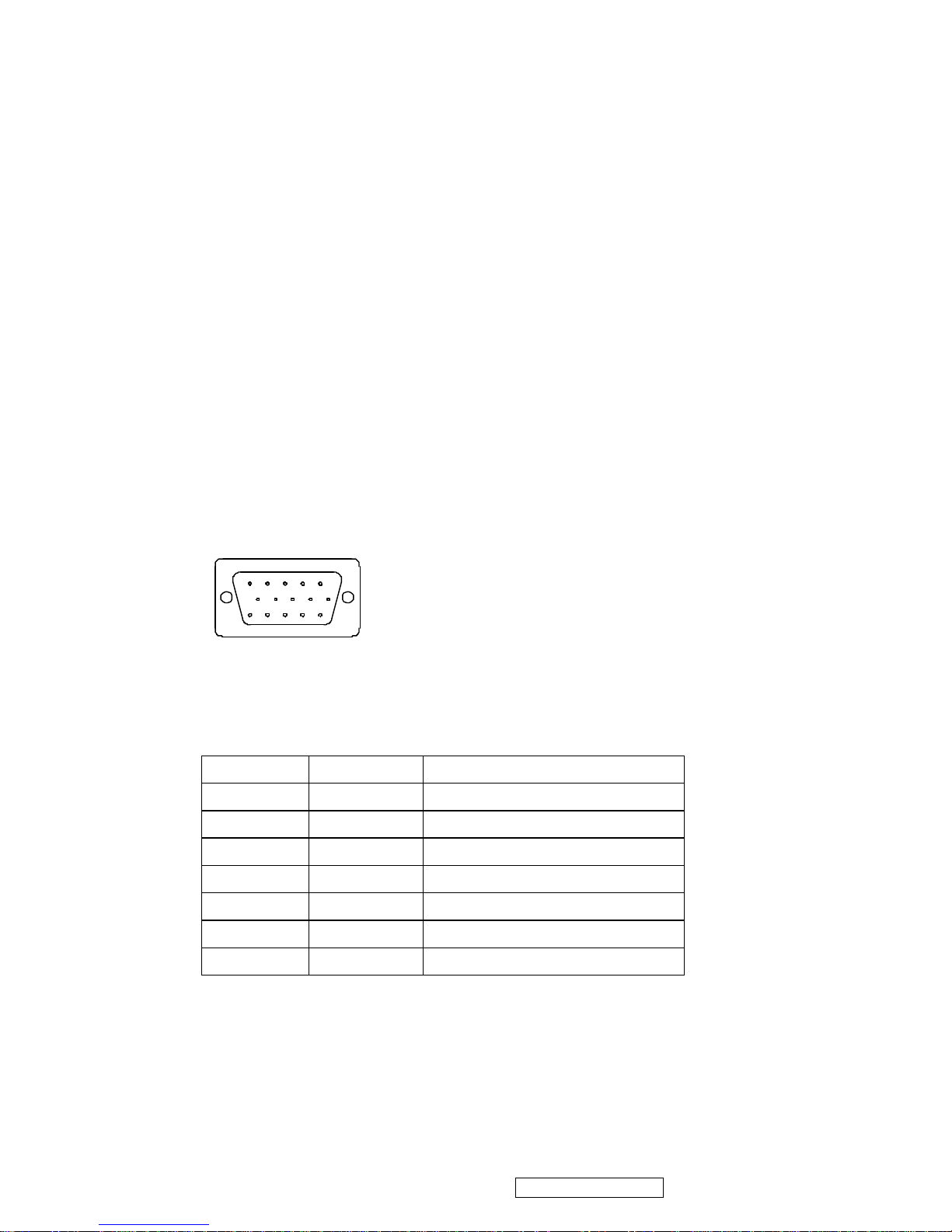
2.3. D-SUB CONNECTOR
D-SUB 15 PIN CONNECTOR
SIGNAL LEVEL
CONNECTOR SIGNAL DE SCRIPTION
R RED 0.7vp-p(VIDEO)
G GREEN 0.7vp-p(VIDEO)
B BLUE 0.7vp-p(VIDEO)
H H/SYNC TTL positive or negative
V V/SYNC TTL positive or negative
SDA DDC1/2B TTL
SCL DDC1/2B TTL
1 2 3 4 5
6 7 8 9 10
11 12 13 14 15
1.R 6.GND 11.NC
2.G 7.GND 12.SDA
3.B 8.GND 13.H.SYNC
4.NC 9. +5V 14.V.SYNC
5.GND 10.GND 15.SCL
ViewSonic Corporation Confidential - Do Not Copy VE710s-4_VE710b-4
3
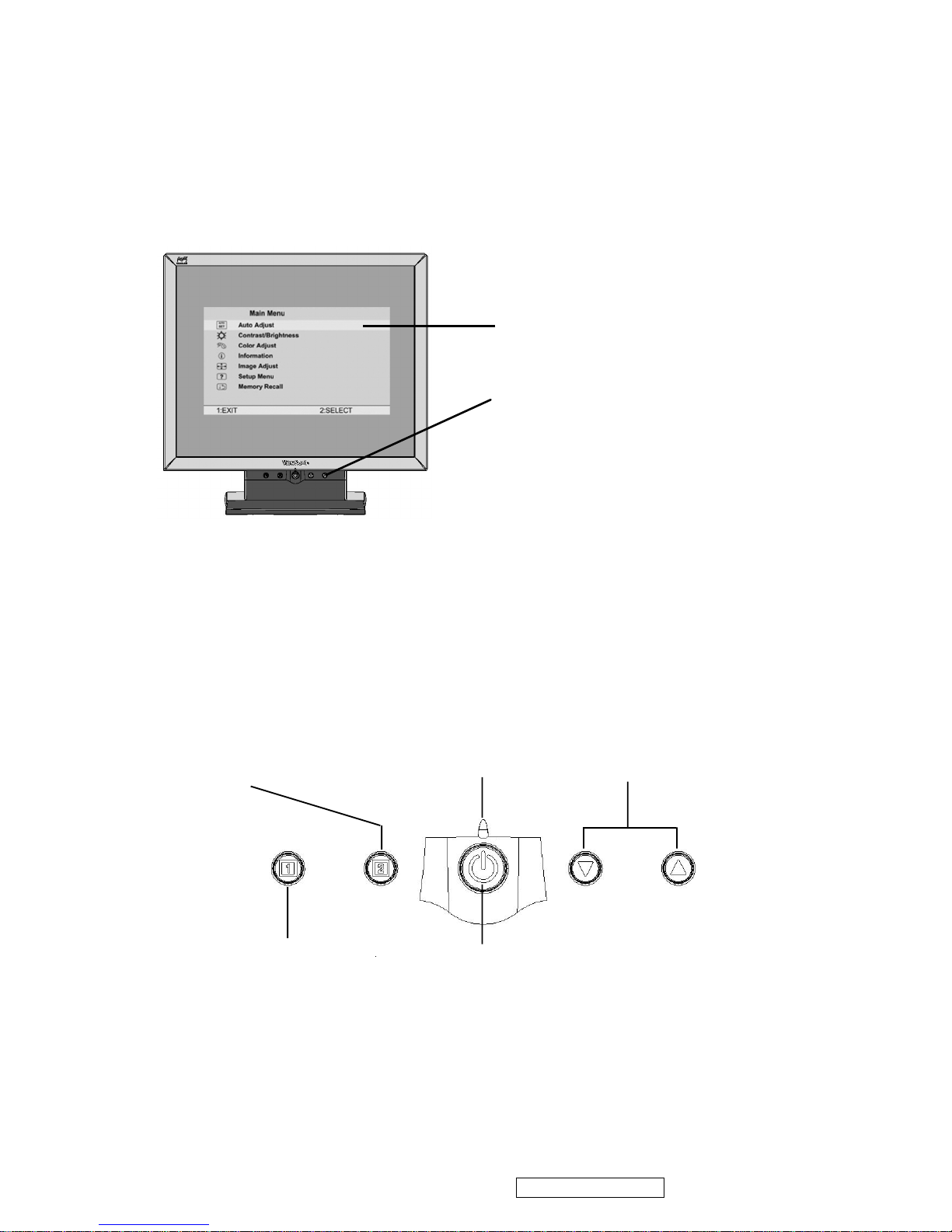
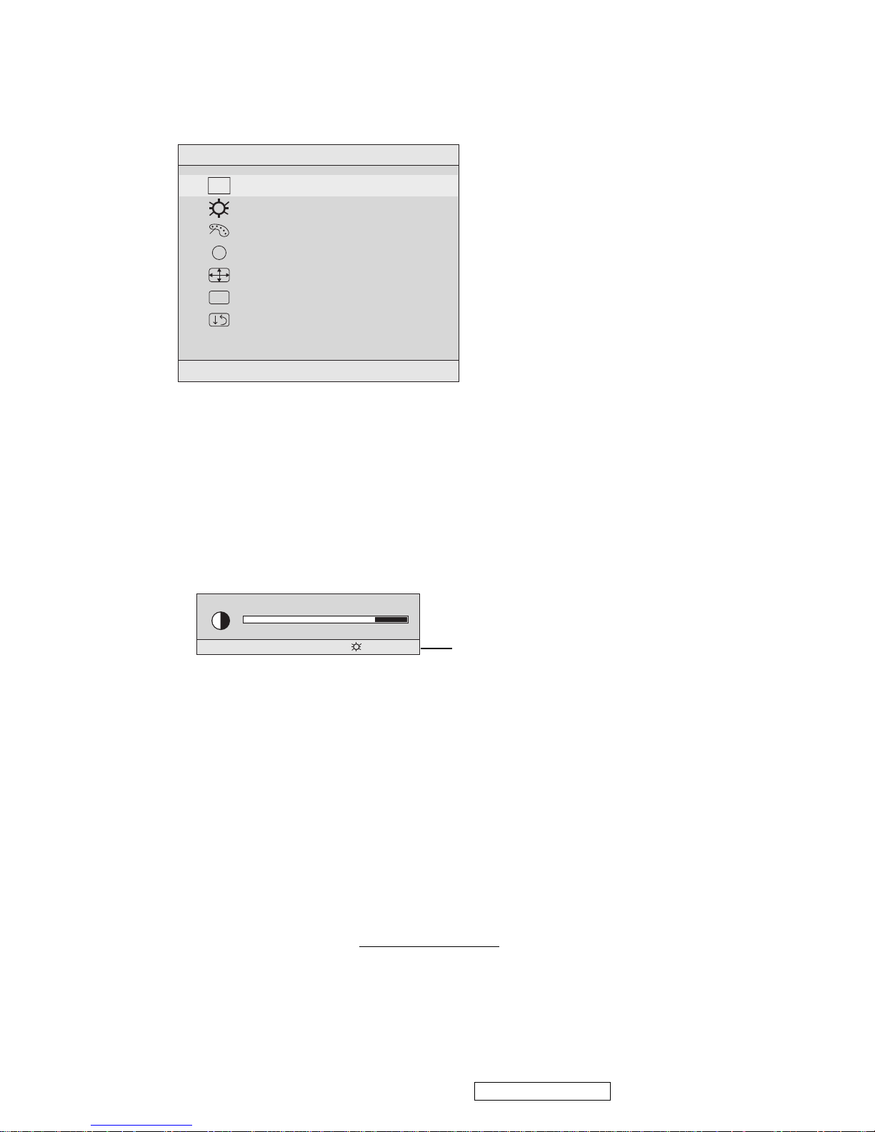
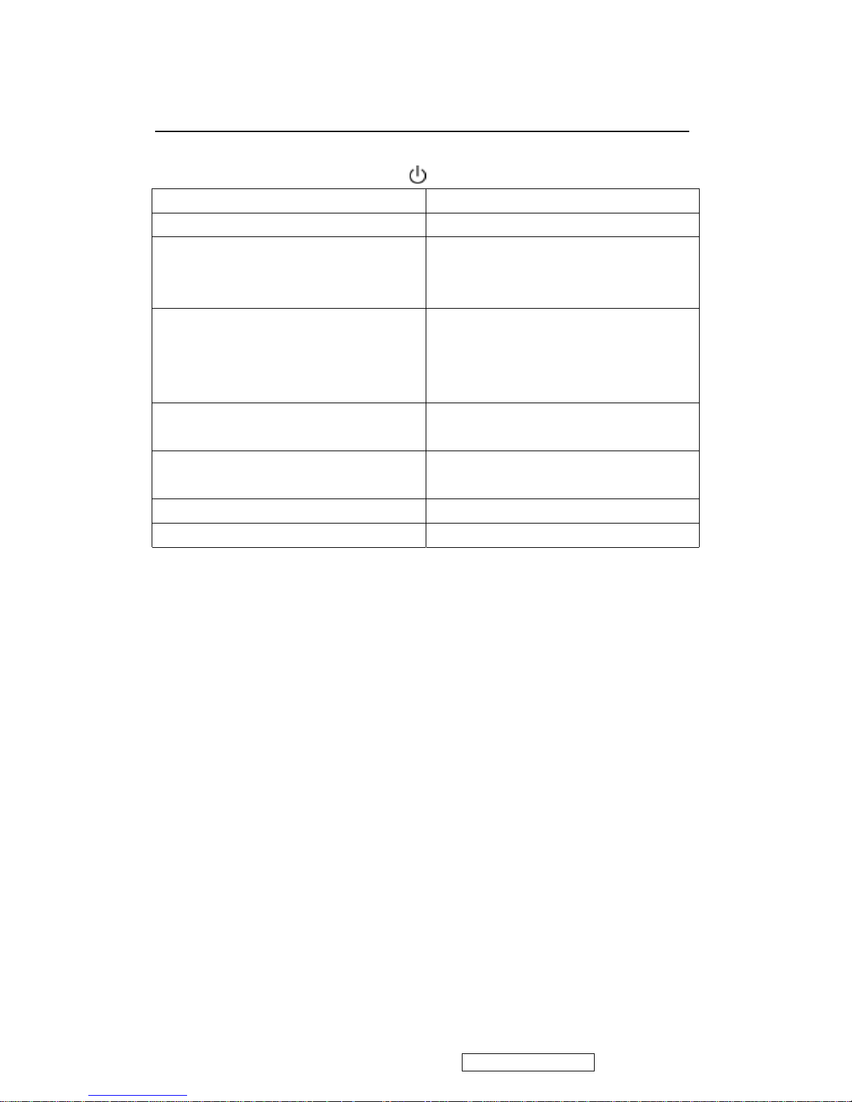
Front Control Panel
shown below in detail
Main Menu
With OnView controls
Scrolls through menu options and
adjusts the displayed control.
Also a shortcut to display the
Contrast adjustment control
screen.
Power
On/Off
Displays the control
screen for the highlighted
control.
Also toggles between two
controls on some
screens.
Also a shortcut to Auto
Image Adjust.
Power light
Green = ON
Orange = Power Saving
Displays the Main Menu
or exits the control screen
and saves adjustments.
3. Front Panel Function Control Description
VE710s-4/VE710b-4
ViewSonic Corporation Confidential - Do Not Copy VE710s-4_VE710b-4
4
. (The black border around the
edge of the screen should barely touch the illuminated “active area” of the
LCD dislay.)
The line at the
bottom of the
screen tells you
what you can do
next: Exit or Select
the control that is
highlighted.
Main Menu
1:EXIT 2:SELECT
Auto Adjust
Contrast/Brightness
Color Adjust
Information
Image Adjust
Setup Menu
Memory Recall
AUTO
SET
i
?
Do the following to adjust the screen image:
1
To display the Main Menu, press button [1].
4
To adjust the control, press the upIor downJbuttons.
5
To save the adjustments and exit the menu, press button [1] twice.
The following tips may help you optimize your display:
• Adjust your computer's graphic card so that it outputs a video signal 1280 x
1024 @ 60 Hz to the LCD dislay. (Look for instructions on “changing the
refresh rate” in your graphic card's user guide.)
• If necessary, make small adjustments using H. POSITION and V. POSITION
until the screen image is completely visible
NOTE: All OnView menus and adjustment screens disappear automatically
after about 15 seconds. This time period is adjustable through the Setup
menu and the OSD timeout control described on page 11.
2
To highlight a control you want to adjust, press I or J to scroll up or down
the Main Menu.
3
To select the highlighted control, press button [2]. A control screen appears
like the example shown below.
Contrast
1:EXIT 2: Brightness
ViewSonic Corporation Confidential - Do Not Copy VE710s-4_VE710b-4
5
Main Menu Controls
Adjust the menu items shown below by using the up Iand down Jbuttons.
Control Explanation
Auto Adjust
automatically sizes, centers, and fine tunes the
video signal to eliminate waviness and distortion.
Press the [2] button to obtain a sharper image.
NOTE
: Auto Adjust works with most common video cards. If
this function does not work on your LCD dislay, then lower the
video refresh rate to 60 Hz and set the resolution to its pre-set
value.
Contrast
adjusts the difference between the image background
(black level) and the foreground (white level).
Brightness
adjusts background black level of the screen image.
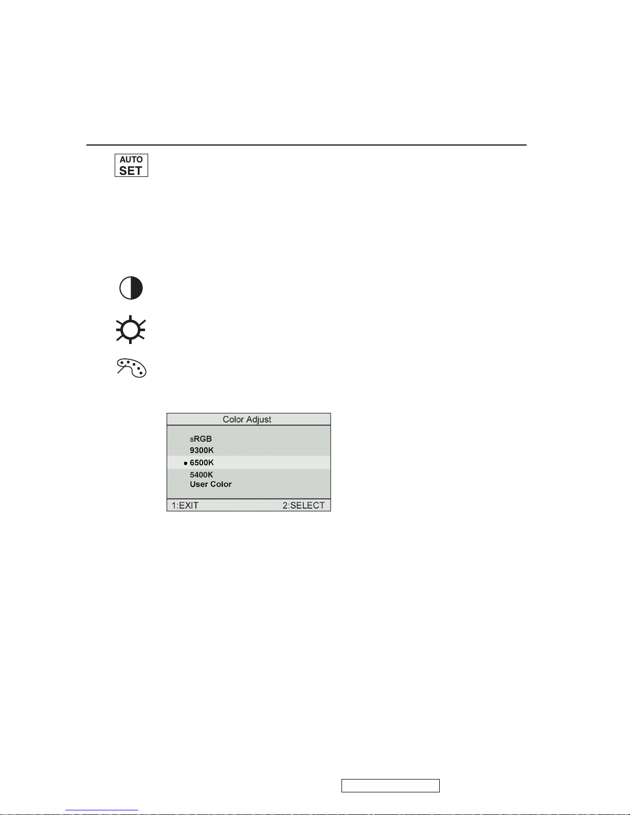
Color Adjust
provides several color options: preset color
temperatures and User which allows you to adjust red (R), green
(G), and blue (B). The factory setting for this product is 6500K
(6500 Kelvin).
6500K
— Adds red to the screen image for warmer white and
richer red. Default setting.
9300K
— Adds blue to the screen image for cooler white (used
in most office settings with fluorescent lighting).
sRGB
— sRGB is quickly becoming the industry standard for color
management, with support being included in many of the latest
applications. Enabling this setting allows the LCD display to
more accurately display colors the way they were originally
intended. Enabling the sRGB setting will cause the Contrast and
Brightness adjustments to be disabled.
5400K — Adds green to the screen image for a darker color.
ViewSonic Corporation Confidential - Do Not Copy VE710s-4_VE710b-4
6
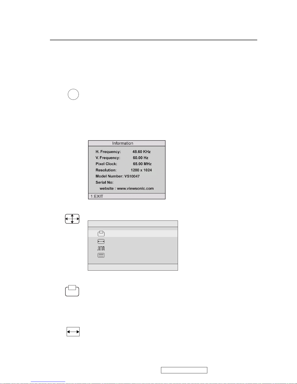
Information
displays the timing mode (video signal input)
coming from the graphics card in your computer. See your
graphic card’s user guide for instructions on changing the
resolution and refresh rate (vertical frequency).
VESA 1280 x 1024 @ 60 Hz (recommended) means that the
resolution is 1280 x 1024 and the refresh rate is 60 Hertz.
Control Explanation
i
H. Size
(Horizontal Size) adjusts the width of the screen image.
NOTE:
Vertical size is automatic with your LCD dislay.
H./V. Position
adjusts horizontal and vertical position of the
screen image. You can toggle between Horizontal and Vertical
by pressing button [2]. Horizontal moves the screen image to
the left or to the right. Vertical moves the screen image up and
down.
Image Adjust
The Image Adjust controls are explained below:
Image Adjust
1:EXIT 2:SELECT
H./V. Position
H. Size
Fine Tune
Sharpness
1
To select color (R, G or B) press button [2].
2
To adjust selected color, press I or J.
3
When you are finished making all color adjustments, press
button [1] twice.
User
— Individual adjustments for red, green, and blue.
ViewSonic Corporation Confidential - Do Not Copy VE710s-4_VE710b-4
7
Fine Tune sharpens focus by aligning the illuminated text and/
or graphic characters.
NOTE: Try the Auto Adjust (see page 9) before using the Fine
Tune control.
Sharpness
adjusts the clarity and focus of the screen image.
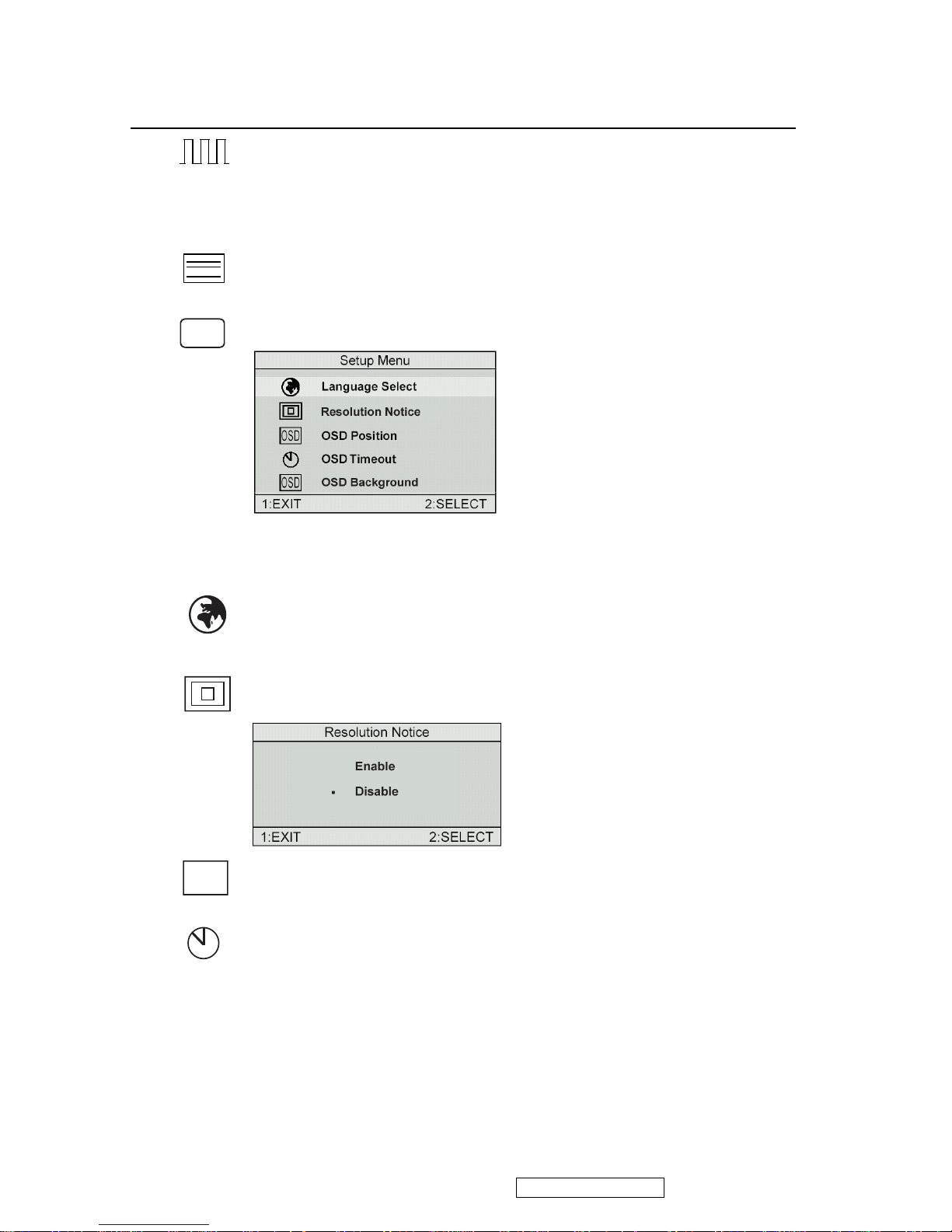
Setup Menu displays the menu shown below.
Explanation
the menus and control screens.
The Setup Menu controls are explained below.
OSD Position
allows you to move the on-screen display menus
and control screens.
OSD Timeout
sets the length of time an on-screen display
screen is displayed. For example, with a “15 second” setting, if
a control is not pushed within 15 seconds, the display screen
disappears.
Resolution Notice
advises the optimal resolution to use.
Language
Select allows you to choose the language used in
OSD
?
Control
ViewSonic Corporation Confidential - Do Not Copy VE710s-4_VE710b-4
8

Memory Recall
returns adjustments to the original factory
settings if the display is operating in a factory Preset Timing
Mode listed in this user guide.
Control Explanation
OSD Background
allows you to turn the On-Screen display
background on or off. This means that while making adjustments
from the OSD control screens you can also view open software
applications, or the Windows desktop.
OSD
ViewSonic Corporation Confidential - Do Not Copy VE710s-4_VE710b-4
9
Short Cut Key
Function Key : 5 Keys !!!! 1 2 ▼
▼▼▼
▲▲▲▲
[1] Main Menu
[2] Auto Image Adjust
[▼▼▼▼] or [▲▲▲▲]
to immediately activate Contrast menu.
It should be change to Brightness OSD
by push button [2].
[▼▼▼▼] + [▲▲▲▲]
recall Contrast or Brightness while in
the Contrast or Brightness adjustment,
or recall both of Contrast and
Brightness when the OSD is not open.
[1] + [2] toggle 720x400 and 640x400 mode when
input 720x400 or 640x400 mode.
[1] + [▼▼▼▼] + [▲▲▲▲]
(Keep pushing 5 sec)
White Balance.
[1] + [▼▼▼▼]
Power Lock
[1] + [▲▲▲▲]
OSD Lock
ViewSonic Corporation Confidential - Do Not Copy VE710s-4_VE710b-4
10

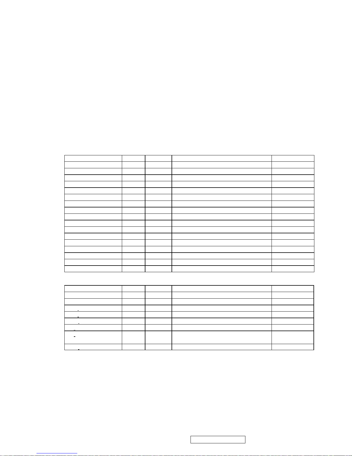
4. Circuit Description (VE710s-4/VE710b-4 M-star Scaler)
A. Scaling controller
The ADC is to convert RGB analog signal to digital signal that scaling chip can acknowledge.
The HSYNC input receives a logic signal and provides the frequency reference for pixel clock generation.
The scaling IC is to converts the input signal ranging from VGA to SXGA into SXGA resolution that panel can
acknowledge.
GENERAL DESCRIPTION
The MST8116A is a high performance, and fully integrated graphics processing IC solution fo r LCD monitors
with resolutions up to SXGA. It is configured with an integrated triple-ADC/PLL, a high quality scaling engine, an
on-screen display controller, a built -in output clock generator, a panel timing controller (TCON), and RSDS
display interface. To further reduce system costs, the MST8116A also integrates intelligent power management
control capability for green-mode requirements and spread-spectrum support for EMI management.
PIN DESCRIPTION
CPU Interface
Pin Name Pin Type Function Pin
HWRESET Schmitt Trigger Input
w/ 5V -tolerant Hardware reset; active high 32
CS Input w/ 5V -tolerant 3 Wire Serial Bus Chip Select; active high 69
SDA I/O w/ 5V -tolerant 3 Wire Serial Bus Data; 4mA driving strength 70
SCL Input w/ 5V -tolerant 3 Wire Serial Bus Clock 71
INT Output CPU interrupt; 4mA driving strength 72
Analog Interface
Pin Name Pin Type Function Pin
HSYNC0 Schmitt Trigger Input
w/ 5V -tolerant Analog HSYNC input 37
VSYNC0 Schmitt Trigger Input
w/ 5V -tolerant Analog VSYNC input 38
REFP Internal ADC top de-coupling pin 66
REFM Internal ADC bottom de-coupling pin 67
RIN0 Analog Input Analog red input 63
RIN0M Analog Input Reference ground for analog red input 62
SOGIN0 Analog Input Sync-on-green input 61
GIN0 Analog Input Analog green input 60
GIN0M Analog Input Reference ground for analog green input 59
BIN0 Analog Input Analog blue input 58
BIN0M Analog Input Reference ground for analog blue input 57
REXT External resistor 390 ohm to AVDD 52
RSDS Interface
Pin Name Pin Type Function Pin
CLKAP Output A-Link Positive RSDS Differential Clock Output from “Odd” Channel 118
CLKAN Output A-Link Negative RSDS Differential Clock Output from “Odd” Channel 119
CLKBP Output B-Link Positive RSDS Differential Clock Output from “Even” Channel 120
CLKBN Output B-Link Negative RSDS Differential Clock Output from “Even” Channel 121
BA[3:1]P Output A-Link Positive RSDS Differential Data Output from “Odd” Channel 92, 90, 88
BA[3:1]N Output A-Link Negative RSDS Differential Data Output from “Odd” Channel 93, 91, 89
GA[3:1]P Output A-Link Positive RSDS Differential Data Output from “Odd” Channel 102, 100, 98
GA[3:1]N Output A-Link Negative RSDS Differential Data Output from “Odd” Channel103, 101,99
RA[3:1]P Output A-Link Positive RSDS Differential Data Output from “Odd” Channel 112, 110, 108
RA[3:1]N Output A-Link Negative RSDS Differential Data Output from “Odd” Channel 113, 111, 109
BB[3:1]P Output B-Link Positive RSDS Differential Data Output from “Even” Channel 4, 128, 124
BB[3:1]N Output B-Link Negative RSDS Differential Data Output from “Even” Channel 5, 1, 125
GB[3:1]P Output B-Link Positive RSDS Differential Data Output from “Even” Channel 14, 12, 8
GB[3:1]N Output B-Link Negative RSDS Differential Data Output from “Even” Channel 15, 13, 9
RB[3:1]P Output B-Link Positive RSDS Differential Data Output from “Even” Channel 24, 22, 16
RB[3:1]N Output B-Link Negative RSDS Differential Data Output from “Even” Channel 25, 23, 17
GPO[8:5] Output TCON GPO[8:5]; 4mA driving strength 29, 28, 30,31
GPO[4:0] Output w/ Pull-down TCON GPO[4:0]; 4~12mA dri ving strength programmable 79-83
OINV Output w/ Pull-down Resistor TCON “Odd” Channel Inversion; 4~12mA driving strength programmable 78
EINV Output w/ Pull-down Resistor TCON “Even” Channel Inversion; 4~12mA driving strength programmable 77
OSP Output w/ Pull-down Resistor TCON “Odd” Channel Start Pulse; 4~12mA driving strength programmable 76
ESP Output w/ Pull-down Resistor TCON “Even” Channel Start Pulse; 4~12mA driving strength programmable 75
GPIO Interface
Pin Name Pin Type Function Pin
ViewSonic Corporation Confidential - Do Not Copy VE710s-4_VE710b-4
11

GOUT1/PWM1 Output GOUT1/PWM1; 4mA driving strength 74
GOUT0/PWM0 Output GOUT0/PWM0; 4mA driving strength 73
Misc. Interface
Pin Name Pin Type Function Pin
BYPASS For External Bypass Capacitor 3
XIN Crystal Oscillator Input Xin 33
XOUT Crystal Oscillator Output Xout 34
Power Pins
Pin Name Pin Type Function Pin
AVDD 3.3V Power ADC Power 45, 51, 55, 65
AVSS Ground ADC Ground 39, 42, 48, 56,
64, 68
AVDD_PLL 3.3V Power PLL Power 53
AVSS_PLL Ground PLL Ground 54
AVDD_MPLL 3.3V Power MPLL Power 35
AVSS_MPLL Ground MPLL Ground 2, 36
VDDP 3.3V Power Digital Output Power 11, 21, 84, 94,
104, 114, 126
GNDP Ground Digital Output Ground 10, 20, 85, 95,
105, 115, 127
VDDC 2.5V Power Digital Core Power 18, 87, 97, 117
GNDC Ground Digital Core Ground 19, 86, 96, 116
No Connects
Pin Name Pin Type Function Pin
NC No Connect. Leave These Pins Floating.
6, 7, 26, 27, 40,
41, 43, 44, 46,
47, 49, 50, 106,
107, 122, 123
Resolution 8 Bits
DC ACCURACY
Differential Nonlinearity ±0.5 +1.50/-1.0 LSB
Integral Nonlinearity ±1 LSB
No Missing Codes Guaranteed
ANALOG INPUT
Input Voltage Range
Minimum 0.5 V p-p
Maximum 1.0 V p-p
Input Bias Current 1 uA
Input Full-Scale Matching 1.5 %FS
Brightness Level Adjustment 62 %FS
SWITCHING PERFORMANCE
Maximum Conversion Rate 165 MSPS
Minimum Conversion Rate 20 MSPS
HSYNC Input Frequency 15 200 kHz
PLL Clock Rate 20 162.5 MHz
PLL Jitter 500 ps p-p
Sampling Phase Tempco TBD ps/°C
DIGITAL INPUTS
Input Voltage, High (VIH) 2.5 V
Input Voltage, Low (VIL) 0.8 V
Input Current, High (IIH) -1.0 uA
Input Current, Low (IIL) 1.0 uA
Input Capacitance 5 pF
DIGITAL OUTPUTS
Output Voltage, High (VOH) VDDP-0.1 V
Output Voltage, Low (VOL) 0.1 V
DYNAMIC PERFORMANCE
Analog Bandwidth, Full Power 250 MHz
Channel to Channel Matching 0.5% Full-Scale
3.3V Supply Voltages VVDD_33 -0.3 3.6 V
2.5V Supply Voltages VVDD_25 -0.3 2.75 V
Input Voltage (5V tolerant inputs) VIN5Vtol -0.3 5.0 V
Input Voltage (non 5V tolerant inputs) VIN -0.3 VVDD_33 V
B. MTV312M64
The MTV312M micro-controller is an 8051 CPU core embedded device especially tailored for CRT/LCD
Monitor applications. It includes an 8051 CPU core, 1024-byte SRAM, 14 built-in PWM DACs, VESA DDC interface, 4-channel A/D
converter, and a 64K-byte internal program Flash -ROM.
A “CMOS output pin” means it can sink and drive at least 4mA current. It is not recommended to use such
pin as input function.
A “open drain pin” means it can sink at least 4mA current bu t only drive 10~20uA to VDD. It can be used as input or output function and needs
ViewSonic Corporation Confidential - Do Not Copy VE710s-4_VE710b-4
12

an external pull up resistor.
A “8051 standard pin” is a pseudo open drain pin. It can sink at least 4mA current when output is at low level, and drives at least 4mA current
for 160nS when output transits from low to high, then keeps driving at 100uA to maintain the pin at high level. It can be used as input or output
function. It needs an external pull up resistor when driving heavy load device.
POWER CONFIGURATION
The MTV312M can work on 5V or 3.3V power supply system.
In 5V power system, the VDD pin is connected to 5V power and the VDD3 needs an external capacitor, all
output pins can swing from 0~5V, input pins can accept 0~5V input range.
And ADC conversion range is 5V. However, X1 and X2 pins must be kept below 3.3V.
In 3.3V power system, the VDD and VDD3 are connected to 3.3V power, all output pins swing from 0~3.3V, HSYNC, VSYNC and open drain
pin can accept 0~5V input range, other pins must be kept below 3.3V. And the ADC conversion range is 3.3V.
C. INVERTER
In order to drive the CCFLs embedded in the panel module, there is a half bridge inverter to convert by the controller.
The input 12V up to hundreds of AC voltage output.
The inverter is formed by symmetric in order to drive the separate lamp modules.
The input stage consists of a PWM controller, half bridge inverter, and switching MOSFET to convert DC input into AC output.
The output stage consists of a tuning capacitor, coupling capacitor, transformer, push-pull MOSFET pair to boost AC output up to hundreds of
voltage.
And one resister is serial to lamp for output voltage feedback.
There are two signal to control the inverter which come from system.
Logic “high” level which send to I901 is turn on the inverter.
BRI signal control brightness by DC level which was integral from PWM signal.
ViewSonic Corporation Confidential - Do Not Copy VE710s-4_VE710b-4
13
Circuit Description (VE710s-4/VE710b-4 Realtek Scaler)
A. Scaling controller
General
l Embedded dual DDC support DDC1, DDC2B,DDC/CI
l Zoom scaling up and down
l Embedded Pattern Generator
l No external memory required.
l Require only one crystal to generate all timing
l Embedded reset control output
l Embedded crystal output to MICROP
l 3 channels 8 bits PWM output, and selectable PWM clock frequency.
PIN DESCRIPTION
(I/O Legend: A= Analog , I=Input ,O=Output ,P=Power ,G=Ground)
■ ADC: 15 pins
Name I/O Pin No Description Note
ADC_ GND AG 27 ADC ground
ADC_REFIO AP 28 ADC band-gap voltage de-coupling 1.20V
ADC_VDD AP 29 Analog power (3.3V)
BLUE+ AI 30 Analog input from BLUE channel
BLUE - AI 31 Analog input ground from BLUE channel
ADC_ GND AG 32 ADC ground
SOG/ADC_TEST AIO 33 SOG in/ADC test pin
GREEN+ AI 34 Analog input from GREEN channel
GREEN- AI 35 Analog input ground from GREEN channel
ADCB_VDD AP 36 Analog power (3.3V)
RED+ AI 37 Analog input from RED channel
RED_ AI 38 Analog input ground from RED channel
ADC_GND AG 39 Analog ground
ADC_GND AG 40 Analog ground
ADC_VDD AP 41 Analog power (3.3V)
AHS AI 42 Analog HS input (10), (4), (5)
AVS AI 43 Analog VS input (2), (4), (5)
■ PLL:8 pins
Name I/O Pin No Description Note
XO AI 1 Reference clock output
XI AO 2 Reference clock input
DPLL GND AG 3 Ground for digital PLL
DPLL VDD AP 4 Power for digital PLL (3.3V)
APLL VDD AP 5 Power for multi-phase PLL (3.3V)
PLL TEST1 AIO 6 Test Pin 1 / IRQ# 3.3V tolerance
PLL TEST2 AIO 7 Test Pin 2/Power -on-latch for crystal out
Frequency
APLL GND AG 8 Ground for multi-phase PLL
ViewSonic Corporation Confidential - Do Not Copy VE710s-4_VE710b-4
14
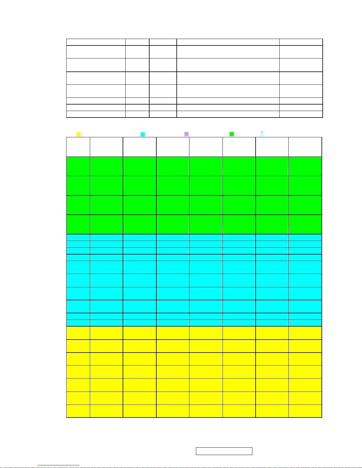
■ Control Interface: 7 pins
Name I/O Pin No Description Note
SDIO [0] IO 54 Serial control I/F data in/Parallel port data
[0]
(2), (3), / 2mA
SDIO [1] / TCON [4] /
BBLU [0]
IO 53 Parallel port data [1] / TCON [4] / TTL
BBLU [0]
(1), (2), (3), /
2mA
SDIO [2] / TCON [3] /
BBLU [1]
IO 52 Parallel port data [1] / TCON [3] / TTL
BBLU [1]
(1), (2), (3), /
2mA
SDIO [3] / PWM2 /
TCON [2]
IO 51 Parallel port data [1] / TCON [4] / PWM2 (1), (2), (3), /
2mA
SCLK I 50 Serial control I/F clock (2), (3), (5)
SCSB I 111 Serial control I/F chip select (2), (3), (5)
RESET O 56 RESET output for Micron (2), (5), (6) / 2mA
■ Display & TCON/VIDEO-8 Port: 54 pins
:LVDS+RSDS+TTLO :RSDS+TTLO :RSDS+TTLIO :TTLO :TTLIO
Pin
NO
6-bits Dual
RSDS
6-bits Single
RSDS
8/6 bits
Dual/Single
LVDS
8 bits
Dual/Single
TTL
6 bits Dual
TTL
6 bits Single
TTL
Note
51 S [3] /
TCON [2] /
PWM2
S 3] /
TCON [2] /
PWM2
S [3] /
TCON [2] /
PWM2
S [3] /
TCON [2] /
PWM2
S [3] /
TCON [2] /
PWM2
S [3] /
TCON [2] /
PWM2
(1), (2), (3), /
2mA
52 S [2] /
TCON [3]
S [2] /
TCON [3]
S [2] /
TCON [3]
S [2] /
BBLU [1] /
TCON [3]
S [2] /
TCON [3]
S [2] /
TCON [3]
(1), (2), (3), /
2mA
53 S [1] /
TCON [4]
S [1] /
TCON [4]
S [1] /
TCON [4]
S [1] /
BBLU [0] /
TCON [4]
S [1] /
TCON [4]
S [1] /
TCON [4]
(1), (2), (3), /
2mA
55 PWM2 /
COUT /
TCON [13]
PWM2 /
COUT /
TCON [13]
PWM2 /
COUT /
TCON [13]
PWM2 /
COUT /
TCON [13]
PWM2 /
COUT /
TCON [13]
PWM2 /
COUT /
TCON [13]
(1), (2), (3), /
2mA
59 BB3P BB3P NC BBLU [7] BBLU [7] BBLU [7]
60 BB3N BB3N NC BBLU [6] BBLU [6] BBLU [6]
61 BB2P BB2P NC BBLU [5] BBLU [5] BBLU [5]
62 BB2N BB2N NC BBLU [4] BBLU [4] BBLU [4]
63 BB1P BB1P NC BBLU [3]
/T0
BBLU [3] BBLU [3]
64 BB1N BB1N NC BBLU [2]
/T1
BBLU [2] BBLU [2]
65 BCLKP BCLKP NC BGRN [1] /
T2
TCON [6] TCON [6]
66 BCLKN BCLKN NC BGRN [0] /
T3
TCON [5] TCON [5]
67 BG3P BG3P NC BGRN [7] BGRN [7] BGRN [7]
68 BG3N BG3N NC BGRN [6] BGRN [6] BGRN [6]
73 BG2P BG2P TODP
BGRN [5] /
T4
BGRN [5] BGRN [5]
74 BG2N BG2N TODN
BGRN [4] /
T5
BGRN [4] BGRN [4]
75 BG1P BG1P TOCLKP
BGRN [3] /
T6
BGRN [3] BGRN [3]
76 BG1N BG1N TOCLKN
BGRN [2] /
T7
BGRN [2] BGRN [2]
77 BR3P BR3P TOCP
BRED [7] /
T8
BRED [7] BRED [7]
78 BR3N BR3N TOCN
BRED [6] /
T9
BRED [6] BRED [6]
79 BR2P BR2P TOBP
BRED [5] /
T10
BRED [5] BRED [5]
ViewSonic Corporation Confidential - Do Not Copy VE710s-4_VE710b-4
15
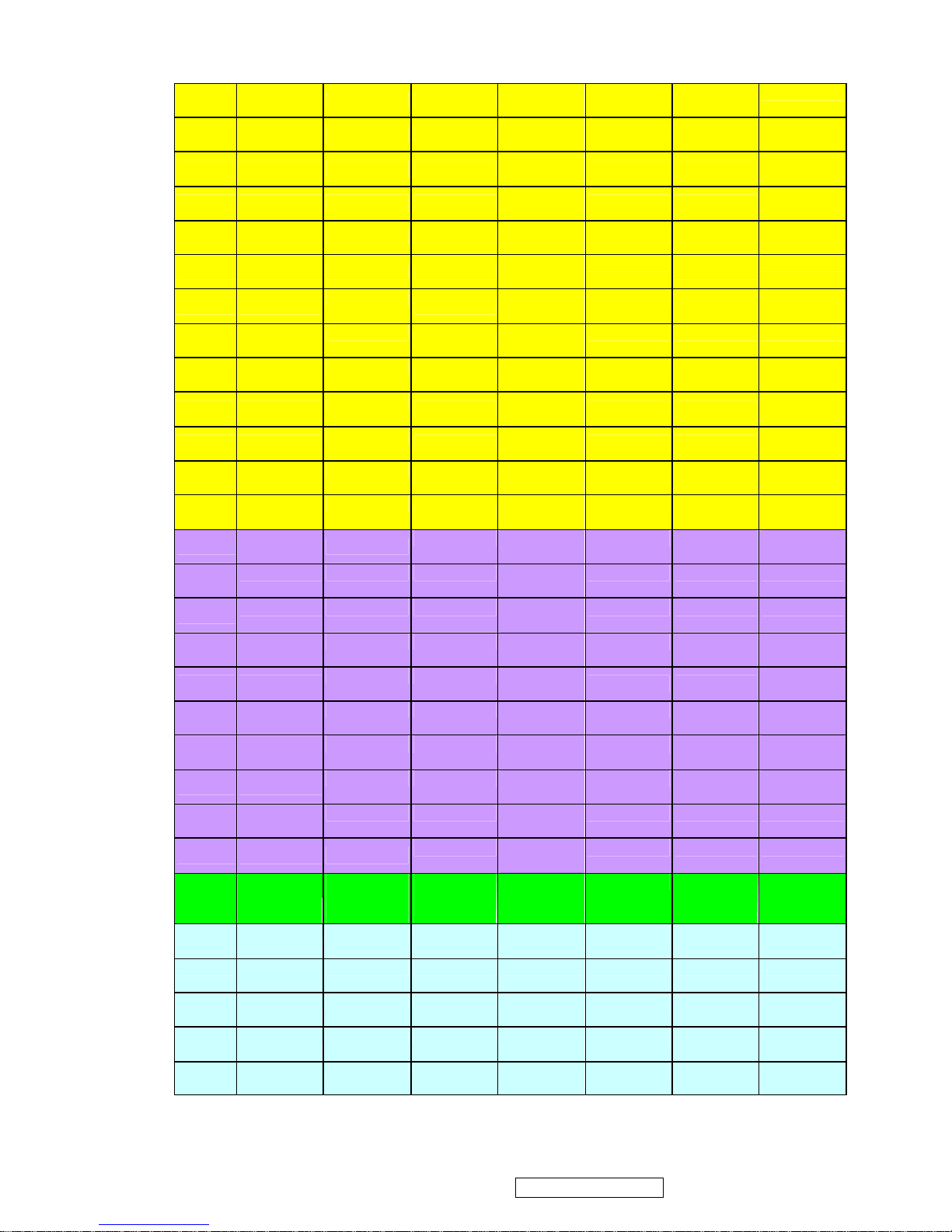
80 BR2N BR2N TOBP
BRED [4] /
T11
BRED [4] BRED [4]
81 BR1P BR1P TOAP
BRED [3] /
T12
BRED [3] BRED [3]
82 BR1N BR1N TOAP
BRED [2] /
T13
BRED [2] BRED [2]
85 AB3P NC TEDP
ABLU [7] /
T14
ABLU [7] ABLU [7]
86 AB3N NC TEDN
ABLU [6] /
T15
ABLU [6] ABLU [6]
87 AB2P NC TECLKP
ABLU [5] /
T16
ABLU [5]
ABLU [5]
88 AB2N
NC
TECLKN
ABLU [4] /
T17
ABLU [4] ABLU [4]
89 AB1P
NC
TECP
ABLU [3] /
T18
ABLU [3] ABLU [3]
90 BB1N
NC
TECN
ABLU [2] /
T19
ABLU [2] ABLU [2]
91 ACLKP
NC
TEBP
ABLU [1] /
T20
TCON [1] TCON [1]
92 ACLKN
NC
TEBN
ABLU [0] /
T21
TCON [0] TCON [0]
93 AG3P
NC
TEAP
AGRN [7] /
T22
AGRN [7] AGRN [7]
94
AG3N NC
TEAN
AGRN [6] /
T23
AGRN [6] AGRN [6]
99
AG2P
TCON [11]
NC AGRN [5] /
T24
AGRN [5] AGRN [5]
100
AG2N TCON [10] NC AGRN [4] /
T25
AGRN [4] AGRN [4]
101
AG1P TCON [9] NC AGRN [3] /
T26
AGRN [3] AGRN [3]
102
AG1N TCON [8] NC AGRN [2] /
T27
AGRN [2] AGRN [2]
103 AR3P
TCON [7] NC ARED [7] /
T28
ARED [7] ARED [7]
104 AR3N
TCON [6] NC ARED [6] /
T29
ARED [6] ARED [6]
105 AR2P
TCON [5] NC ARED [5] /
TH
ARED [5] ARED [5]
106 AR2N
TCON [1] NC ARED [4] /
TV
ARED [4] ARED [4]
107 AR1P
TCON [0] NC ARED [3] /
TE
ARED [3] ARED [3]
108 AR1N NC
NC ARED [2] /
TK
ARED [2] ARED [2]
113 PWM2 /
COUT /
TCON [12]
PWM2 /
COUT /
TCON [12]
PWM2 /
COUT /
TCON [12]
ARED [1] COUT PWM2 /
COUT /
TCON [12]
(9)
114 TCON [11]
/V [0]
V [0] V [0] ARED [0] TCON [11] (1), (7), (8)
115 TCON [10]
/V [1]
V [1] V [1] BRED [1] TCON [10] (1), (7), (8)
116 TCON [9] /
V [2]
V [2] V [2] BRED [0] TCON [9] (1), (7), (8)
117 TCON [8] /
V [3]
V [3] V [3] AGRN [1] TCON [8] (1), (7), (8)
118 TCON [7] /
V [4]
V [4] V [4] AGRN [0] TCON [7] (1), (7), (8)
ViewSonic Corporation Confidential - Do Not Copy VE710s-4_VE710b-4
16
119 TCON [6] /
V [5]
V [5] V [5] DHS DHS DHS (1), (7), (8)
122 TCON [5] /
V [6]
V [6] V [6] DVS DVS DVS (1), (7), (8)
123 TCON [1] /
V [7]
V [7] V [7] DENA
DENA DENA (1), (7), (8)
124 TCON [0] /
VCLK
VCLK VCLK DCLK DCLK DCLK (1), (7), (8)
*Single RSDS, even/odd swap, data (59~82) output to pin85~108, TCON (99~108) output to pin59~68.
*In 6-bit dual TTL output mode, Video8 cannot output TCON7~TCON11; while video8 can output TCON in
6-bit single TTL mode.
■ TMDS: 18 pins
Name I/O Pin No Description Note
TMDS_TST/ PWM1 AIO 9 TMDS_TEST Pin / PWM1 / Power-on-latch
for serial / parallel port
TMDS_GND G 10
TMDS_VDD P 11 (3.3V)
NC A 12 Impedance Match Reference.
TMDS_VDD P 13 (3.3V)
NC I 14 Differential Data Input
NC I 15 Differential Data Input
TMDS_GND G 16
NC I 17 Differential Data Input
NC I 18 Differential Data Input
TMDS_VDD P 19 (3.3V)
NC I 20 Differential Data Input
NC I 21 Differential Data Input
TMDS_GND G 22
NC I 23 Differential Data Input
NC I 24 Differential Data Input
TMDS_GND G 25
TMDS_VDD P 26 (3.3V)
■ PWM Interface: (PWM1, PWM2 can be selected from 1 of 3 possible pins.)
Name I/O Pin No Description Note
PWM2 / TCON [2] / S
[3]
O 51 PWM2 / TCON [2] / SDIO [3] (1), (2), (3), (5),
(8),
PWM2 / TCON [13] /
COUT
O 55 PWM2 / TCON [13] / Crystal out (2), (8), (9)
PWM2 / TCON [12] /
COUT
O 113 PWM2 / TCON [12] / Crystal out (2), (8), (9) 6bit
dual TTL cannot
support
PWM1 / TMDS_TST AIO 9 PWM1/ TMDS_TEST Pin/ Power-on-latch
for serial / parallel port
(2), (7), (8)
PWM1 / DDCSDA /
TCON [1] / BBLU [0]
IO 47 PWM1 / DDC serial control I/F data input /
output / TCON [4]
(1), (2), (3), (5),
(8),
PWM1 / TCON [7] IO 125 PWM1 / TCON [7] (1), (2), (3), (5),
(8),
PWM0 / REFCLK IO 112 PWM0 / (In / out) test pin for DCLK /
Video8 even-odd signal
(2), (9)
ViewSonic Corporation Confidential - Do Not Copy VE710s-4_VE710b-4
17
■ DDC Channel:4 pins
Name I/O Pin No Description Note
DDCSCL/TCON [0] /
BBLU [1]
I 46 DDC serial control I/F clock/TCON [0]/TTL
BBLU [1]
(2), (3), (5)
DDCSDA/TCON [1] /
PWM1/BBLU [0]
IO 47 DDC serial control I/F data input/ output/
TCON [1]/ PWM1/ TTL BBLU [0]
(1), (2), (3), (5),
(6), (8)/8mA/no
slew
TCON [5] I 126 TCON [5] (2), (3), (5)
TCON [7]/PWM1 IO 125 TCON [7]/ PWM1 (1), (2), (3), (5),
(6), (8)/8mA/no
slew
■ Power & Ground:22 pins
Name I/O Pin No Description
3.3V Power P 49,121 VCCIO: 2
3.3V Ground G 48,120 GNDIO: 2
3.3V Power P 58,71,83, 95,110 PVCC: 5
3.3V Ground G 57,72,84,96,109 PGND: 5
2.5V Power P 45,69,98,127 VCCK: 4
2.5V Ground G 44,70,97,128 GNDK: 4
Note: (1) TTL compatible CMOS Input (Vt=1.7V); VCC=3.3V;
(2) 5V tolerance pad;
(3) Internal 75K Ohms pull high resistor.
(4) Internal 75K Ohms pull low resistor.
(5) Schmitt trigger CMOS Input (Vt=1.4~2.2V);
(6) Open-Drain, Output Drive low & Pull-high.
(7) Bi-directional input/output
(8) Programmable driving current (2~10mA)
(9) TTL output 5V & 3.3V
(10) 4V tolerance pad
B. MTV312M64
The MTV312M micro-controller is an 8051 CPU core embedded device especially tailored for CRT/LCD
Monitor applications. It includes an 8051 CPU core, 1024-byte SRAM, 14 built-in PWM DACs, VESA DDC interface, 4-channel A/D
converter, and a 64K-byte internal program Flash -ROM.
A “CMOS output pin” means it can sink and drive at least 4mA current. It is not recommended to use such
pin as input function.
A “open drain pin” means it can sink at least 4mA current but only drive 10~20uA to VDD. It can be used as input or output function and needs
an external pull up resistor.
A “8051 standard pin” is a pseudo open drain pin. It can sink at least 4mA current when output is at low level, and drives at least 4mA current
for 160nS when output transits from low to high, then keeps driving at 100uA to maintain the pin at high level. It can be used as input or output
function. It needs an external pull up resistor when driving heavy load device.
POWER CONFIGURATION
The MTV312M can work on 5V or 3.3V power supply system.
In 5V power system, the VDD pin is connected t o 5V power and the VDD3 needs an external capacitor, all
output pins can swing from 0~5V, input pins can accept 0~5V input range.
And ADC conversion range is 5V. However, X1 and X2 pins must be kept below 3.3V.
In 3.3V power system, the VDD and VDD3 are connected to 3.3V power, all output pins swing from 0~3.3V, HSYNC, VSYNC and open drain
pin can accept 0~5V input range, other pins must be kept below 3.3V. And the ADC conversion range is 3.3V.
C. INVERTER
In order to drive the CCFLs embedded in the panel module, there is a half bridge inverter to convert by the controller.
The input 12V up to hundreds of AC voltage output.
The inverter is formed by symmetric in order to drive the separate lamp modules.
The input stage consists of a PWM controller, half bridge inverter, and switching MOSFET to convert DC input into AC output.
The output stage consists of a tuning capacitor, coupling capacitor, transformer, push-pull MOSFET pair to boost AC output up to hundreds of
voltage.
And one resister is serial to lamp for output voltage feedback.
There are two signal to control the inverter which come from system.
Logic “high” level which send to I901 is turn on the inverter.
BRI signal control brightness by DC level which was integral from PWM signal.
ViewSonic Corporation Confidential - Do Not Copy VE710s-4_VE710b-4
18

5. Adjusting Procedure (VE710s-4/VE710b-4)
5.1. ADJUSTMENT CONDITIONS AND PRECAUTIONS
1. Approximately 30 minutes should be allowed for warm up before proceeding.
2. Adjustments should be undertaken only on those necessary elements since most of them have been carefully
preset at the factory.
3. ESD protection is needed before adjustment.
5.2. MAIN ADJUSTMENTS
NO. FUNCTION DESIGNATION
1. White Balance Function Key
2. GEOMETRY Function Key
5.3. ALIGNMENT PROCEDURES
Adjustment Conditions and Precautions:
(A). Power supply voltage:
AC 110/120V±10% 60 Hz±5%, AC 220/240V±10% 50 Hz ±5%.
(B). Warm up time:
The display must be power ON for at least 30 minutes at full white pattern before starting alignments.
This is especially critical in color temperature and white balance adjustments.
(C). Signals: reference the front detail specifications and timing table.
Video : reference the front detail specifications.
1. Adjustment of White Balance:
A. TIMING: 1280x1024 64KHz/60Hz.
B. PATTERN: 5 Blocks.
C. LCD MONITOR set to 1280x1024 80K/75Hz BURN IN and warm up over 30 minutes.
D. CA110 color analizer at the center of screen and along a perpendicular to the screen at 20cm from the
display.
E. Power turn off, Press
“▲” and “ ”
and turn on power at the same time after power LED is on,
release
“▲” and “ ”
key, Then press “ ” key go to factory mode. (Fig.1)
F. Adjust Color Temperature:
(1) EEPROM INIT (5 BLOCKS):
Press “▼” key move cursor to EEPROM INIT, Press key then monitor will INIT ADC value.
(2) Press “▲” key move cursor to “White Balance”, Press key do white balance adjustment.
(3) Press “▼” key move cursor to “Color Temerature Adjust”, Press key, Then OSD will display
Fig.2
1 2 2
(Fig.1)
2 2 2
ViewSonic Corporation Confidential - Do Not Copy VE710s-4_VE710b-4
19
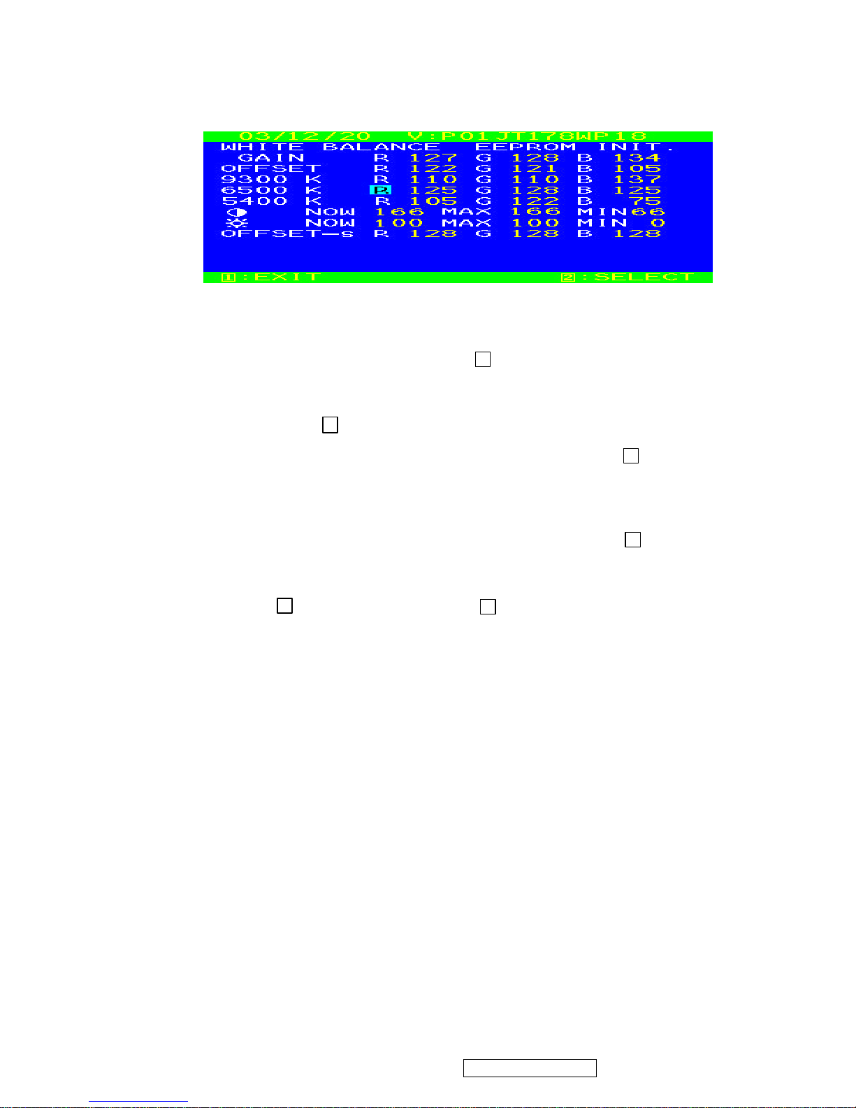
(4) 9300K verify: move cursor to 9300K Press key.
Press “▼” ,“▲” key adjust R.G .B value
x=0.283 ±0.02
y=0.298 ±0.02
Press key return to Fig.2
(5) 6500K verify: Repeat (4) press “▼” ,“▲” move cursor to 6500K press key
x=0.313 ±0.02
y=0.329 ±0.02
Y≧240 cd/m2
(6) 5400K verify: Repeat (4) press “▼” ,“▲” move cursor to 5400K press key
x=0.332 ±0.02
y=0.348 ±0.02
(7) Press key go back to Fig.2, Then press key return to Fig.1, Power key
OFF/ON quit factory mode.
G. Color Temperature & Luminance Verify:
BRIGHTNESS MAX, CONTRAST MAX
9300K: x=0.283 ±0.02 y=0.298 ±0.02
6500K: x=0.313 ±0.02 y=0.329 ±0.02 Y ≧240 cd/㎡(CPT Panel) Y≧230 cd/㎡(CMO Panel)
5400K: x=0.332 ±0.02 y=0.348 ±0.02
2. Geometry:
(a). Set cross-hatch pattern and preset timing as timing table listed.
(b). Change to each mode in turn and wait for the monitor finish auto-alignment and save process befor e
change to next mode.
(c). Until all of modes are agjusted, exit OSD menu and press PWR OFF to exit factory mode.
(Fig.2)
2 1 2 2 1 1
ViewSonic Corporation Confidential - Do Not Copy VE710s-4_VE710b-4
20
Firmware update procedure :
(VE710s-4/VE710b-4)
When you received a received mo nitor , please check whether the firmware version. If not , please
followning procedures to upgrade to the latest version .
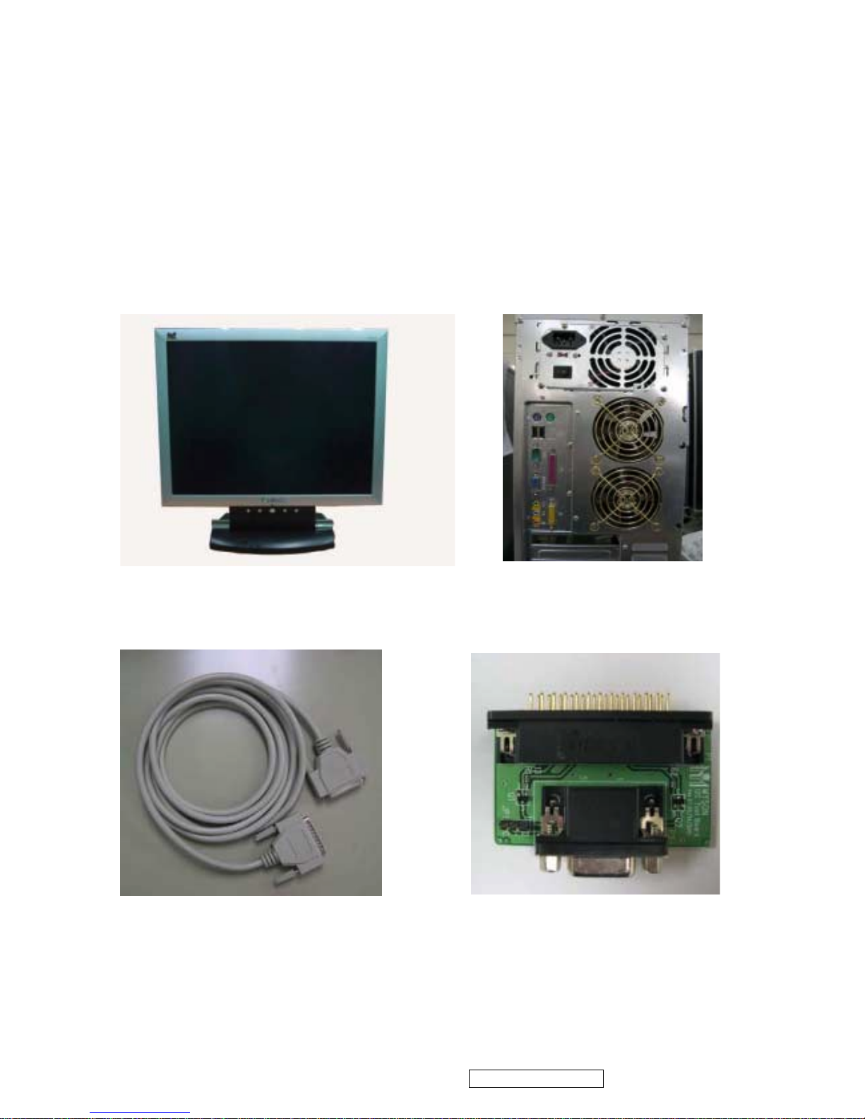
1. Equipment needed :
˘
VA721/VE710s-4/VE710b-4
˘
PC ( Personal computer )
˘
LPT cable
˘
Fixture (LM5ISP )
˘
Firmware upgrade program
ViewSonic Corporation Confidential - Do Not Copy VE710s-4_VE710b-4
21
2. Connection :
Appendix A : How to install the software for ISP :
1. To setup ISP Environment :
Hardware: PC or notebook, parallel(printer) cable, ISP tooling.
Software: If OS was win2000 or WinXP , please install "PORT95NT.exe"
In order to ensure can execute ISP program, please set BIOS in PC or Notebook as Fig 0.0
To PC
To Monitor
Fig 0.0
ViewSonic Corporation Confidential - Do Not Copy VE710s-4_VE710b-4
22
2. Double-click the " PORT95NT.exe" in W indows & initall the program. , see Fig 0.1
3. Keep on press " Next " 4 t imes to go through the install ation processes, see Fig. 0.2
Fig 0.1
Fig. 0.2
ViewSonic Corporation Confidential - Do Not Copy VE710s-4_VE710b-4
23
4. Choose " Typical " then press " Next " , see Fig. 0.3
5. Keep on press " Next " 4 t imes to go through the install ation processes, see Fig. 0.4
Fig. 0.3
Fig. 0.4
ViewSonic Corporation Confidential - Do Not Copy VE710s-4_VE710b-4
24
 Loading...