


Service Manual
ViewSonic Q9b-3
Model No. VS11455
19” Color TFT LCD Display
(Q9b-3_SM Rev. 1a Sep. 2006)
ViewSonic 381 Brea Canyon Road, Walnut, California 91789 USA - (800) 888-8583
Copyright
Copyright © 2006 by ViewSonic Corporation. All rights reserved. No part of this publication
may be reproduced, transmitted, transcribed, stored in a retrieval system, or translated into any
language or computer language, in any form or by any means, electronic, mechanical, magnetic,
optical, chemical, manual or otherwise, without the prior written permission of ViewSonic
Corporation.
Disclaimer
ViewSonic makes no representations or warranties, either expressed or implied, with respect to
the contents hereof and specifically disclaims any warranty of merchantability or fitness for any
particular purpose. Further, ViewSonic reserves the right to revise this publication and to make
changes from time to time in the contents hereof without obligation of ViewSonic to notify any
person of such revision or changes.
Trademarks
Optiquest is a registered trademark of ViewSonic Corporation.
ViewSonic is a registered trademark of ViewSonic Corporation.
All other trademarks used within this document are the property of their respective owners.
Revision History
Revision SM Editing Date ECR Number Description of Changes Editor
1a 9/15/2006 Initial Release Jamie Chang
ViewSonic Corporation Confidential - Do Not Copy Q9b-3
i

TABLE OF CONTENTS
1. Precautions and Safety Notices 1
2. Specification 4
3. Front Panel Function Control Description 7
4. Circuit Description 12
5. Adjustment Procedure 17
6. Troubleshooting Flow Chart 38
7. Recommended Spare Parts List 43
8. Exploded Diagram and Exploded Parts List 51
9. Block Diagram 55
10. Schematic Diagrams 56
11. PCB Layout Diagrams 64
ViewSonic Corporation Confidential - Do Not Copy Q9b-3
ii

1. Precautions and Safety Notices
1. Appropriate Operation
(1) Turn off the product before cleaning.
(2) Use only a dry soft cloth when cleaning the LCD panel surface.
(3) Use a soft cloth soaked with mild detergent to clean the display housing.
(4) Disconnect the power plug from AC outlet if the product is not used for a long period of
time.
(5) If smoke, abnormal noise, or strange odor is present, immediately switch the LCD display
off.
(6) Do not touch the LCD panel surface with sharp or hard objects.
(7) Do not place heavy objects on the LCD display, video cable, or power cord.
(8) Do not use abrasive cleaners, waxes or solvents for your cleaning.
(9) Do not operate the product under the following conditions:
- Extremely hot, cold or humid environment.
- Areas susceptible to excessive dust and dirt.
- Near any appliance generating a strong magnetic field.
- Place in direct sunlight.
2. Caution
No modification of any circuit should be attempted. Service work should only be performed after
you are thoroughly familiar
with all of the following safety checks and servicing guidelines.
3. Safety Check
Care should be taken while servicing this LCD display. Because of the high voltage used in the
inverter circuit, the voltage is exposed in such areas as the associated transformer circuits.
4. Power Supply Requirements
The external AC power operating range shall be from 90 to 264Vac
5. LCD Module Handling Precautions
5.1. Handling Precautions
(1) Since front polarizer is easily damaged, pay attention not to scratch it.
(2) Be sure to turn off power supply when inserting or disconnecting from input connector.
(3) Wipe off water drop immediately. Long contact with water may cause discoloration or
spots.
(4) When the panel surface is soiled, wipe it with absorbent cotton or other soft cloth.
(5) Since the panel is made of glass, it may break or crack if dropped or bumped on hard
surface.
(6) Since CMOS LSI is used in this module, take care of static electricity and insure human
earth when handling.
(7) Do not open nor modify the Module Assembly.
(8) Do not press the reflector sheet at the back of the module to any directions.
(9) In case if a Module has to be put back into the packing container slot after once it was
taken out from the container, do not press the center of the CCFL Reflector edge.
Instead, press at the far ends of the CFL Reflector edge softly. Otherwise the TFT
Module may be damaged.
(10) At the insertion or removal of the Signal Interface Connector, be sure not to rotate nor
tilt the Interface Connector of the TFT Module.
(11) After installation of the TFT Module into an enclosure (LCD monitor housing, for
example), do not twist nor bend the TFT Module even momentary. At designing the
enclosure, it should be taken into consideration that no bending/twisting forces are
applied to the TFT Module from outside. Otherwise the TFT Module may be damaged.
(12) Cold cathode fluorescent lamp in LCD contains a small amount of mercury. Please
follow local ordinances or regulations for disposal.
(13) Small amount of materials having no flammability grade is used in the LCD module.
ViewSonic Corporation Confidential - Do Not Copy Q9b-3
1
The LCD module should be supplied by power complied with requirements of Limited
Power Source (IEC60950 or UL1950), or be applied exemption.
(14) The LCD module is designed so that the CFL in it is supplied by Limited Current
Circuit (IEC60950 or UL1950). Do not connect the CFL in Hazardous Voltage Circuit.
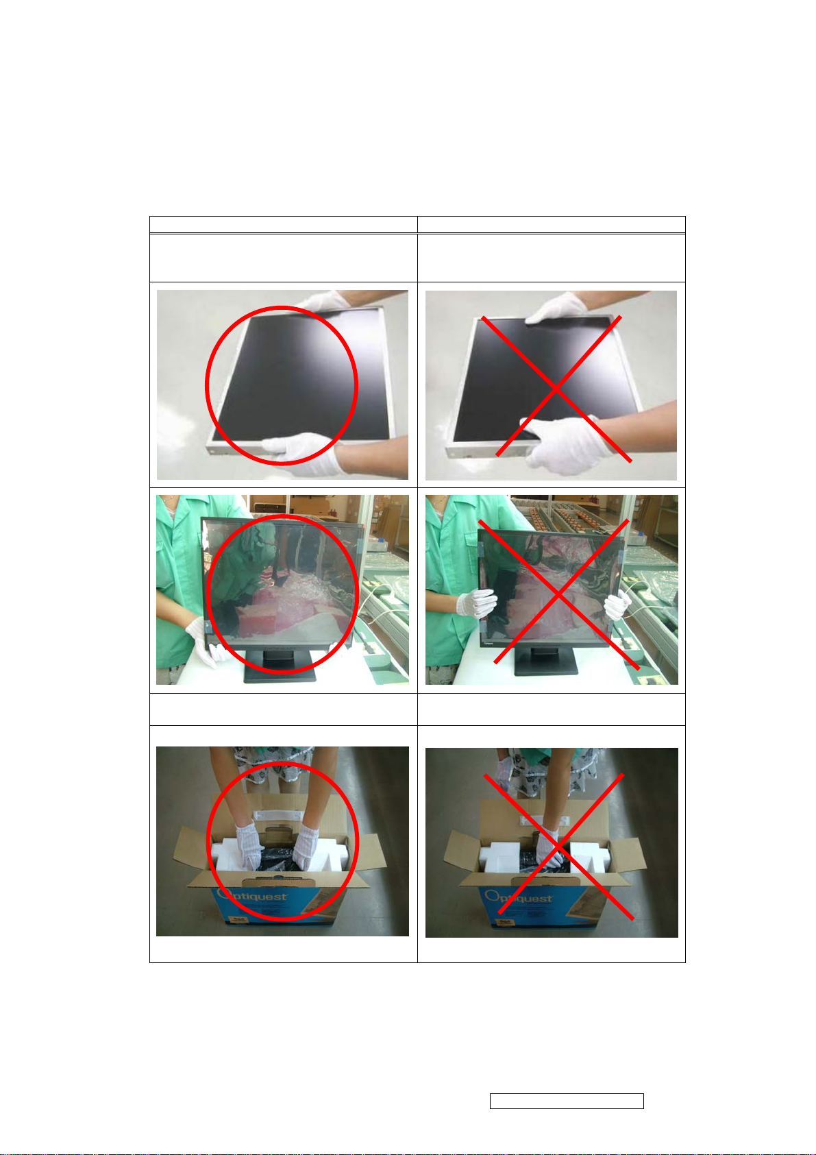
5.2. Handling and Placing Methods
Correct Methods: Incorrect Methods:
Only touch the metal frame of the LCD panel
or the front cover of the monitor. Do not touch
the surface of the polarizer.
Take out the monitor with cushions Taking out the monitor by grasping the LCD
Surface of the LCD panel is pressed by fingers
and that may cause “Mura”
panel. That may cause “Mura”
ViewSonic Corporation Confidential - Do Not Copy Q9b-3
2
Place the monitor on a clean and soft foam pad. Placing the monitor on foreign objects. That
could scratch the surface of the panel or cause
“Mura”
ViewSonic Corporation Confidential - Do Not Copy Q9b-3
3
2. Specification
1. General Requirements
General Specifications
Test Resolution & Frequency “1280 x 1024” @ 60Hz
Test Image Size Full Size
Contrast and Brightness Controls Factory Default:
Contrast =100%, Brightness = 100%
2. Signal Interface
Video Interface
Analog Input Connector DB-15 (Analog)
Default Input Connector Defaults to the first detected input
Video Cable Connector DB-15 Pin out Compliant DDC 1/2B.
Video Signals 1. Video RGB (Analog) Separate Sync
Video Impedance 75 Ohms (Analog), 100 Ohms (Digital)
Exclusions Not compatible with interlaced video.
3. Power
Power Supply
Input Voltage Range 90 to 264 VAC
Power Dissipation 37Watts (Typ.)
4. Electrical Requirements
Horizontal / Vertical Frequency
Horizontal Frequency 30 – 80 KHz
Vertical Refresh Rate 56– 75 Hz
* For resolution 1280 x 1024, the vertical
Refresh rate up to 75 Hz; for there rest
Resolutions, the vertical refresh rate up
To 75Hz.
Maximum Pixel Clock 135 MHz.
Sync Polarity Independent of sync polarity.
Timing Table
Item Timing Analog
1 640 x 480 @ 60Hz, 31.5kHz Yes
2 640 x 480 @ 67Hz, 35.0kHz Yes
3 640 x 480 @ 75Hz, 37.5kHz Yes
4 720 x 400 @ 70Hz, 31.5kHz Yes
5 800 x 600 @ 56Hz, 35.1kHz Yes
6 800 x 600 @ 60Hz, 37.9kHz Yes
7 800 x 600 @ 75Hz, 46.9kHz Yes
8 800 x 600 @ 72Hz, 48.1kHz Yes
9 832 x 624 @ 75Hz, 49.7kHz Yes
10 1024 x 768 @ 60Hz, 48.4kHz Yes
11 1024 x 768 @ 70Hz, 56.5kHz Yes
12 1024 x 768 @ 75Hz, 60.0kHz Yes
13 1280 x 1024 @ 60Hz, 63.4kHz Yes
14 1280 x 1024 @ 75Hz, 79.97kHz Yes
Changing Modes
Maximum Mode Change Blank Time for image
stability. Note:
1) Excluding “Auto Adjust” time
2) Under DOS mode (640 x 350, 720 x 400 & 640 x
400), there is no “Auto Adjust” feature.
3) The monitor needs to do “Auto Adjust” the first
time a new mode is detected.
Under 5 seconds (Maximum)
1 seconds (Typ.) for recognized timings
1-2 seconds (Typ.) for unrecognized timing
ViewSonic Corporation Confidential - Do Not Copy Q9b-3
4
5. LCD Panel
Panel Characteristics
st
Souce:
1
Panel Type HSD190ME13-A02
Type TN type with LVDS interface
Active Size 376.32 (H) x 301.06 (V)
Pixel Arrangement RGB Vertical Stripe
Pixel Pitch 0.294 mm
# of Backlights 4 CCFL edge-light (2 top / 2 bottom)
Backlight Life 40,000 Hours (minimum)
Panel Performance
Luminance –
Condition:
CT = 6500K, Contrast = Max,
250 cd/m2 (typ. after 30-minute warm-up)
Brightness = Max
Brightness Uniformity ≥ 80% Entire Area(Typ)
Contrast Ratio 600:1 (typ.), 450:1 (minimum)
Color Depth 16.2M colors (6-bits+2 bits FRC)
Viewing Angle (Horizontal) 140 degrees @ CR>10
Viewing Angle (Vertical) 130 degrees @ CR>10
Response Time
8ms(Typ.)
10%-90% @ Ta=25°C
nd
2
Panel Type 2
and 3
rd
Source:
nd
panel source : HSD190ME13-A10
rd
Panel source : HSD190ME13-A16
3
Type TN type with LVDS interface
Active Size 376.32 (H) x 301.056 (V)
Pixel Arrangement RGB Vertical Stripe
Pixel Pitch 0.294 mm
# of Backlights 4 CCFL edge-light (2 top / 2 bottom)
Backlight Life 40,000 Hours (minimum)
Panel Performance
Luminance –
Condition:
CT = 6500K, Contrast = Max,
300 cd/m2 (typ. after 30-minute warm-up)
Brightness = Max
Brightness Uniformity 75%(Typ)/70%min
Contrast Ratio 700:1 (typ.), 450:1 (minimum)
Color Depth 16.2million colors (6 bits+2bits data)
Viewing Angle (Horizontal) 160degrees @ CR>10
Viewing Angle (Vertical) 155 degrees @ CR>10
Response Time
8ms (Typ.)
10%-90% @ Ta=25°C
6. Mechanical
Dimensions
Width 407 mm
Height 414 mm
Depth 200 mm
Monitor Weight 4.85kg / 10.67 lbs
Ergonomics
Tilt Up 20 DEGREES MINIMUM
Tilt Down -5 degrees
ViewSonic Corporation Confidential - Do Not Copy Q9b-3
5

Package Specifications
Width 465 mm
Height 445 mm
Depth 150 mm
Gross Weight 5.55kg (12.21 lbs)
7. Environmental
Environmental Conditions
Operating Temperature 0°C to +40°C
Storage Temperature -20°C to +60°C
Operating Relative Humidity 10% to 90% RH Non-Condensing
Storage Relative Humidity 5% to 90% RH Non-Condensing
Operating Altitude 0 to +3,000 meters
Storage Altitude 0 to +12,000 meters
ViewSonic Corporation Confidential - Do Not Copy Q9b-3
6
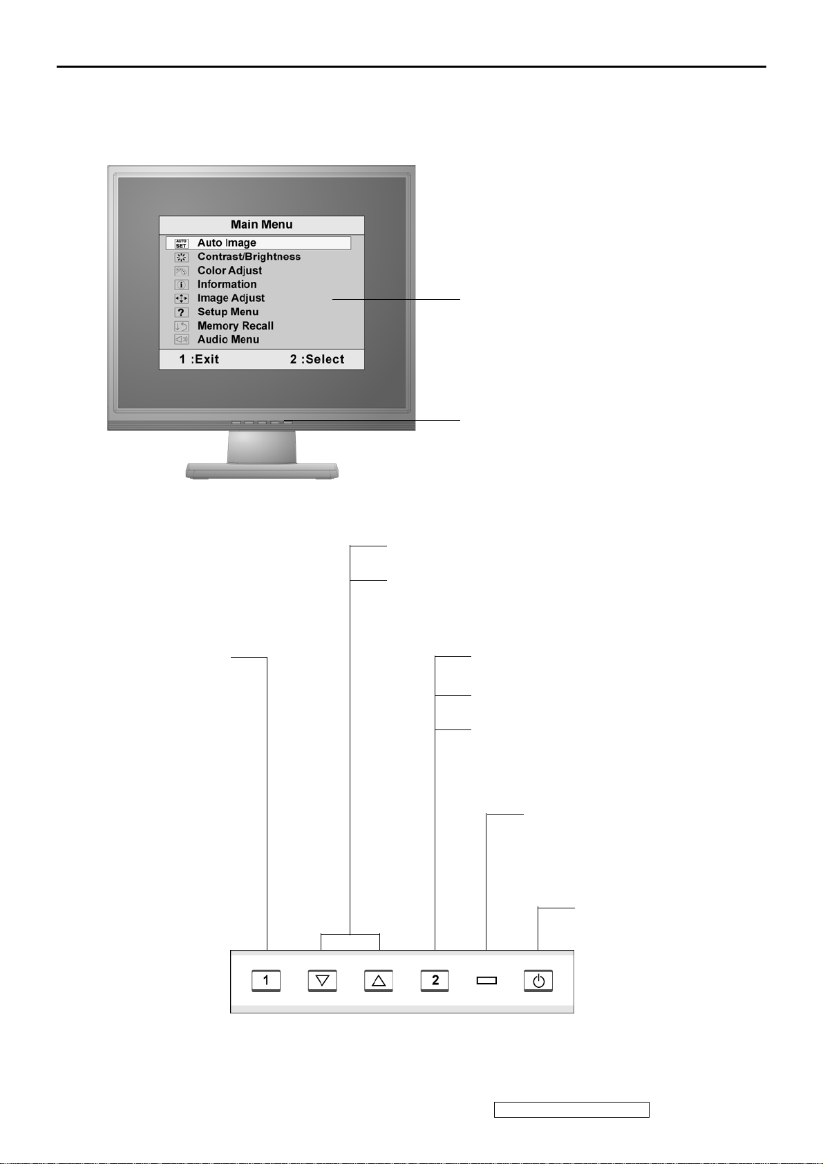
3. Front Panel Function Control Description
Main Menu
with OSD controls
Front Control Panel
shown below in detail
Displays the Main
Menu or exits the
control screen and
saves adjustments.
Scrolls through menu options and adjusts the
displayed control.
Also a shortcut to display the Contrast adjustment
control screen.
Displays the control screen for the
highlighted control.
Also toggles between two controls on
some screens.
Also a shortcut to Auto Image Adjust.
Power light
Green = ON
Orange = Power Saving
Standby Power
On/Off
ViewSonic Corporation Confidential - Do Not Copy Q9b-3
7
Do the following to adjust the display setting:
1. To display the Main Menu, press button [1].
NOTE: All OSD menus and adjustment screens disappear automatically after about 30
seconds. This is adjustable through the OSD timeout setting in the setup menu.
2. To select a control to adjust, pressSorTto scroll up or down in the Main Menu.
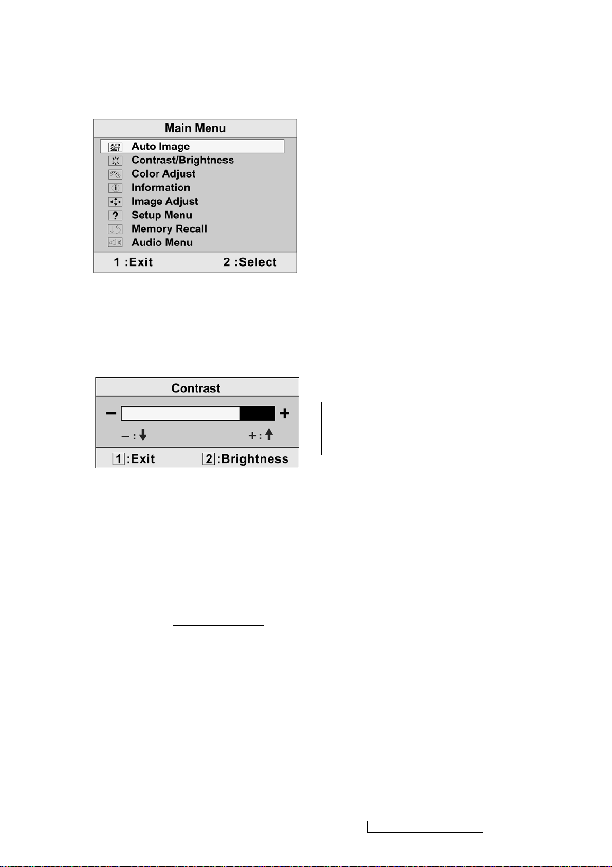
3. After the desired control is selected, press button [2]. A control screen like the one shown
below appears.
The line at the bottom of the screen
shows the current functions of buttons 1
and 2: Exit or select the Brightness
control.
4. To adjust the setting, press the upSor downTbuttons.
5. To save the adjustments and exit the menu, press button [1] twice.
The following tips may help you optimize your display:
• Adjust the computer's graphics card so that it outputs a 1280 x 1024 @ 60Hz video signal to
the LCD display. (Look for instructions on “changing the refresh rate” in the graphics card's
user guide.)
• If necessary, make small adjustments using H. POSITION and V. POSITION until the
screen image is completely visible
. (The black border around the edge of the screen should
barely touch the illuminated “active area” of the LCD display.)
ViewSonic Corporation Confidential - Do Not Copy Q9b-3
8
Main Menu Controls
Adjust the menu items shown below by using the upSand downTbuttons.
Control Explanation
Auto Image Adjust automatically sizes, centers, and fine tunes the video signal
to eliminate waviness and distortion. Press the [2] button to obtain a sharper
image.
NOTE: Auto Image Adjust works with most common video cards. If this
function does not work on your LCD display, then lower the video refresh rate
to 60 Hz and set the resolution to its pre-set value.
Contrast adjusts the difference between the image background (black level)
and the foreground (white level).
Brightness adjusts background black level of the screen image.
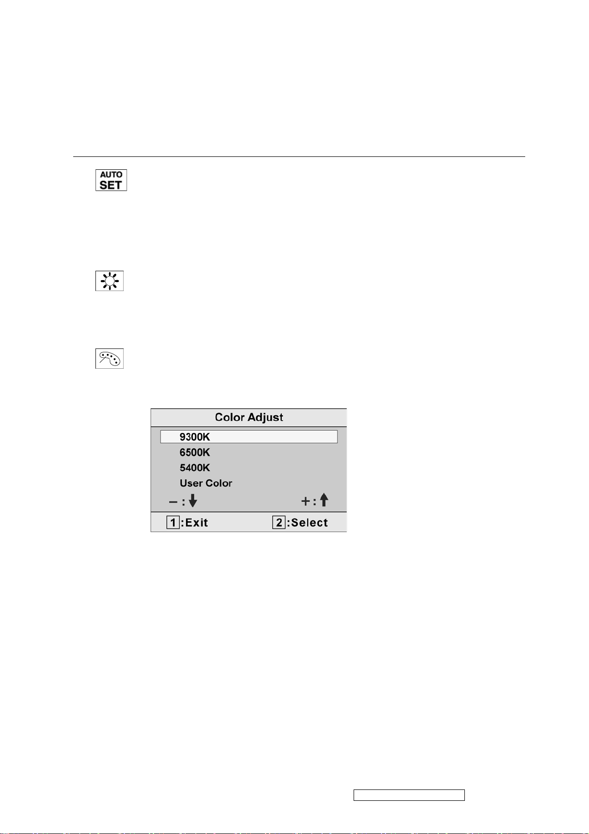
Color Adjust provides several color adjustment modes, including preset color
temperatures and a User Color mode which allows independent adjustment of
red (R), green (G), and blue (B). The factory setting for this product is 6500K
(6500 Kelvin).
9300K-Adds blue to the screen image for cooler white (used in most office
settings with fluorescent lighting).
6500K-Adds red to the screen image for warmer white and richer red.
5400K-Adds green to the screen image for a darker color.
User Color Individual adjustments for red (R), green (G), and blue (B).
1. To select color (R, G or B) press button [2].
2. To adjust selected color, pressSorT.
Important: If you select RECALL from the Main Menu when the product is set
to a Preset Timing Mode, colors return to the 6500K factory preset.
ViewSonic Corporation Confidential - Do Not Copy Q9b-3
9
Control Explanation
Information displays the timing mode (video signal input) coming from the
graphics card in the computer, the LCD model number, the serial number, and
®
the ViewSonic
instructions on changing the resolution and refresh rate (vertical frequency).
NOTE: VESA 1280 x 1024 @ 60Hz (recommended) means that the resolution
is 1280 x 1024 and the refresh rate is 60 Hertz.
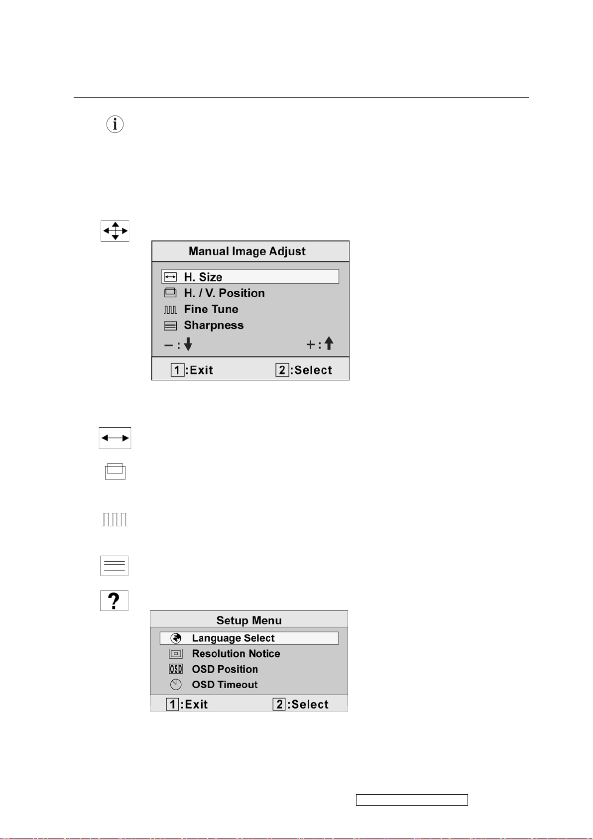
Manual Image Adjust displays the Manual Image Adjust menu.
website URL. See your graphics card’s user guide for
The Manual Image Adjust controls are explained below:
H. Size (Horizontal Size) adjusts the width of the screen image.
H./V. Position (Horizontal/Vertical Position) moves the screen image left or
right and up or down.
Fine Tune sharpens the focus by aligning the text and/or graphics with pixel
boundaries.
Sharpness adjusts the clarity and focus of the screen image.
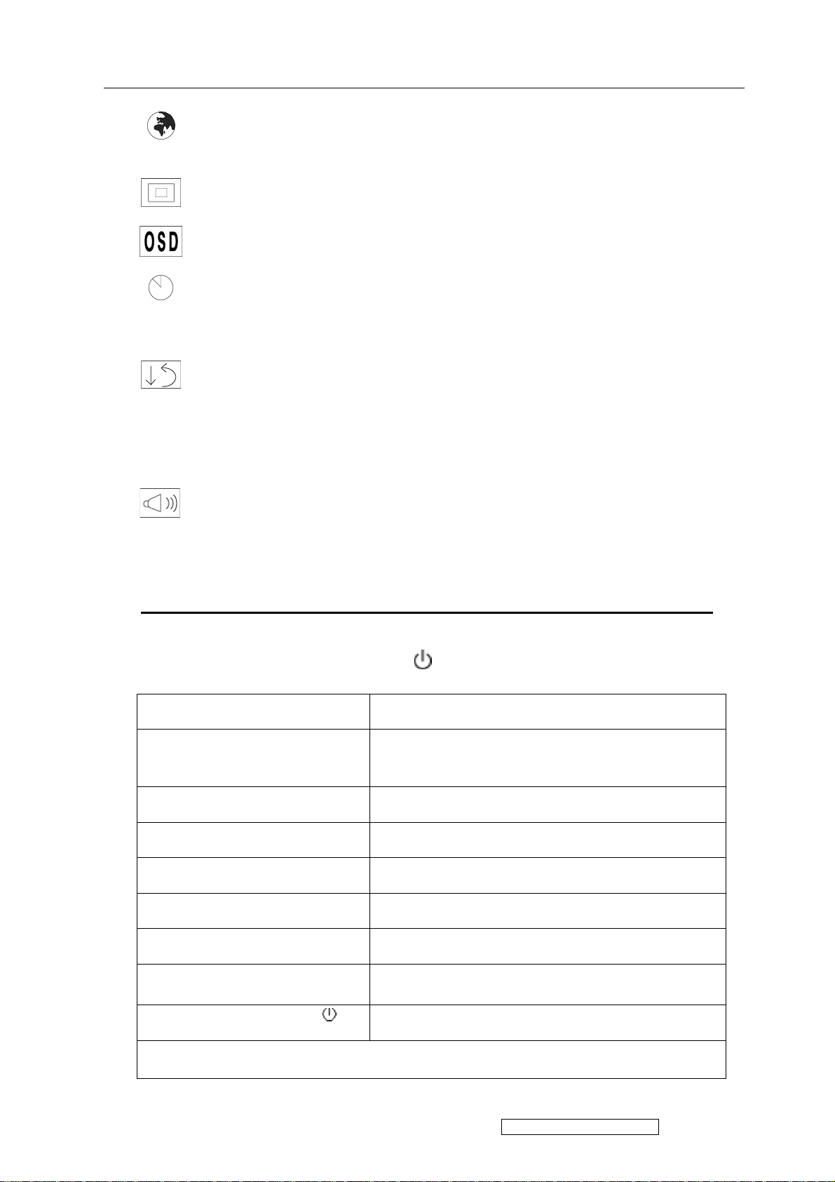
Setup Menu displays the menu shown below:
The Setup Menu controls are explained below:
ViewSonic Corporation Confidential - Do Not Copy Q9b-3
10
Control Explanation
Language Select allows the user to choose the language used in the menus and
control screens.
Resolution Notice advises the optimal resolution to use.
OSD Position allows the user to move the OSD menus and control screens.
OSD Timeout sets the length of time the OSD screen is displayed. For example,
with a “15 second” setting, if a control is not pushed within 15 seconds, the
display screen disappears.
Memory Recall returns the adjustments back to factory settings if the display is
operating in a factory Preset Timing Mode listed in the Specifications of this
manual.
Exception: This control does not affect changes made with the User Color
control, Language or Power Lock setting.
Audio Adjust
Vol ume increases the volume, decreases the volume, and mutes the audio.
Mute temporarily silences audio output.
Short Cut Key
Function Key : 5 Keys !!!! 1 2 ▼
[▼]+ [▲]
[1] Main Menu
[2] 1. Auto Image Adjust
2. toggle 720x400 and 640x400 mode when input
720x400 or 640x400 mode
[▼]
[▲]
to immediately activate Brightness menu.
to immediately activate Contrast menu.
recall both of Contrast and Brightness to default
▼▼▼
▲▲▲▲
[1] + [▼]
[1] + [▲]
[▼]+ [▲] +
No signal message OSD
Signal + [▲] + [2] + [ ]
Remark : All the short cuts function are only available while OSD off (exclude Power
Lock and OSD Lock)
Power Lock
OSD Lock
Burning mode
Factory Mode
ViewSonic Corporation Confidential - Do Not Copy Q9b-3
11
4. Circuit Description
A. DC-DC CONVERTER
This brick convert is the 110-220AC input voltage to 12V AND 5V output for invert use and
panel use and system controller use .
5V Out put at L804
VCC 12V In put at L803,F901
B. Scaling controller
The ADC is to convert RGB analog signal to digital signal that scaling chip can acknowledge.
The HSYNC input receives a logic signal and provides the frequency reference for pixel clock
generation.
The scaling IC is to converts the input signal ranging from VGA to SXGA into SXGA
resolution that panel can acknowledge.
The scaling IC is to converts the input signal ranging from VGA to SXGA into SXGA
resolution that panel can acknowledge.
GENERAL DESCRIPTION
The TSUM16AK is total solution graphics processing IC for LCD monitors with panel
resolutions up to SXGA. It is configured with a high-speed integrated triple-ADC/PLL, a high
quality display processing engine, and an integrated output display interface that can support
LVDS panel interface format. To further reduce system costs, the TSUM16AK also integrates
intelligent power management control capability for green-mode requirements and
spread-spectrum support for EMI management.
The TSUM16AK incorporates the world’s first coherent oversampled RGB graphics ADC in a
monitor controller system1. The oversampling ADC samples the input RGB signals at a
frequency that is much higher than the signal source pixel rate. This can preserve details in the
video signal that ordinarily would be lost due to input signal jitter or bandwidth limitations in
non-oversampled systems.
The TSUM16AK also incorporates a new Dynamic Frame Rate (DFR) generator2 for the
digital output video to the display panel that preserves the advantages of a fixed output clock
rate, while eliminating the output end of frame short-line.
PIN DESCRIPTION
Analog Interface
Pin Name Pin Type Function Pin
HSYNC0
VSYNC0
REFP
REFM
Schmitt Trigger Input
w/ 5V-tolerant
Schmitt Trigger Input
w/ 5V-tolerant
Analog
HSYNC
Analog VSYNC input
Internal ADC top de-coupling pin 62
Internal ADC bottom de-coupling pin 61
input
63
64
RIN0P Analog Input Analog red input 59
RIN0M Analog Input Reference ground for analog red input 58
SOGIN0 Analog Input Sync-on-green input 57
GIN0P Analog Input Analog green input 56
GIN0M Analog Input
BIN0P Analog Input
BIN0M Analog Input
REXT
Reference ground for analog
green
Analog
blue
Reference ground for analog
blue
External resistor 390 ohm to AVDD_ADC 51
input 54
input 55
input 53
ViewSonic Corporation Confidential - Do Not Copy Q9b-3
12
Serial Flash Interface
Pin Name Pin Type Function Pin
SDO Input w/ 5V-Tolerant
CSZ Output SPI Flash Chip Select 71
SCK Output SPI Flash Serial Clock 72
SDI Output
LVDS Interface
Pin Name Pin Type Function
LVA0M Output
LVA0P Output
LVA1M Output
LVA1P Output
LVA2M Output
LVA2P Output
LVA3M Output
LVA3P Output
LVACKM Output
Pin Name Pin Type Function Pin
LVACKP Output
LVB0M Output
LVB0P Output
LVB1M Output
LVB1P Output
LVB2M Output
LVB2P Output
LVB3M Output
LVB3P Output
LVBCKM Output
LVBCKP Output
SPI Flash
Serial
SPI Flash
Serial
A-Link Negative LVDS
Differential
A-Link Positive LVDS
Differential
A-Link Negative LVDS
Differential
A-Link Positive LVDS
Differential
A-Link Negative LVDS
Differential
A-Link Positive LVDS
Differential
A-Link Negative LVDS
Differential
A-Link Positive LVDS
Differential
A-Link Negative LVDS Differential Clock
Output
A-Link Positive LVDS Differential Clock
Output
B-Link Negative LVDS
Differential
B-Link Positive LVDS
Differential
B-Link Negative LVDS
Differential
B-Link Positive LVDS
Differential
B-Link Negative LVDS
Differential
B-Link Positive LVDS
Differential
B-Link Negative LVDS
Differential
B-Link Positive LVDS
Differential
B-Link Negative LVDS Differential Clock
Output
B-Link Positive LVDS Differential Clock
Output
Data Output 70
Data Input 73
Data
Output
Data
Output
Data
Output
Data
Output
Data
Output
Data
Output
Data
Output
Data
Output
Data
Output
Data
Output
Data
Output
Data
Output
Data
Output
Data
Output
Data
Output
Data
Output
Pin
114
113
112
111
110
109
106
105
108
107
127
126
125
124
123
122
119
118
121
120
ViewSonic Corporation Confidential - Do Not Copy Q9b-3
13
GPIO Interface
Pin Name Pin Type Function Pin
GPIO_P12 I/O w/ 5V-tolerant
PWM1/
GPIO_P25
GPIO_P00/
SAR1
GPIO_P01/
SAR2
GPIO_P02/
SAR3
GPIO_P03 I/O w/ 5V-tolerant
GPIO_P06 I/O w/ 5V-tolerant
GPIO_P07 I/O w/ 5V-tolerant
PWM0/
GPIO_P26
GPIO_P13 I/O w/ 5V-tolerant General
GPIO_P14 I/O w/ 5V-tolerant General
GPIO_P16/
PWM2
I/O w/ 5V-tolerant
I/O w/ 5V-tolerant
I/O w/ 5V-tolerant
I/O w/ 5V-tolerant
I/O w/ 5V-tolerant
I/O w/ 5V-tolerant
General Purpose Input/Output; 4mA
programmable driving strength
Pulse Width Modulation Output; 4mA
driving strength/ General Purpose
Input/Output; 4mA driving strength
General Purpose Input/Output; 4mA driving
strength/ SAR ADC Input
General Purpose Input/Output; 4mA driving
strength/ SAR ADC Input
General Purpose Input/Output; 4mA driving
strength/ SAR ADC Input
General Purpose Input/Output; 4mA
programmable driving strength
General Purpose Input/Output; 6/12mA
programmable driving strength
General Purpose Input/Output; 6/12mA
programmable driving strength
Pulse Width Modulation Output; 4mA
driving strength/ General Purpose
Input/Output; 4mA driving strength
Purpose Input/Output; 4mA
driving strength
Purpose Input/Output; 4mA
driving strength
General
Pulse
W
Purpose Input/Output; 4mA
driving strength/ idth Modulation
Output; 4mA driving strength
20
21
23
24
25
26
27
28
29
30
31
35
Pin Name Pin Type Function Pin
GPIO_P15
/PWM0
GPIO_P23
GPIO_P22
GPIO_P11/
I2C_MDA
GPIO_P10/
I2C_MCL
PWM2/
GPIO_P24
GPIO_P27
/PWM1
I/O w/
5V-tolerant
I/O w/
5V-tolerant
I/O w/
5V-tolerant
I/O w/
5V-tolerant
I/O w/
5V-Tolerant
I/O w/
5V-tolerant
I/O w/
5V-tolerant
General Purpose Input/Output; 4mA driving strength/ 69
Pulse Width Modulation Output; 4mA driving strength
General Purpose Input/Output; 4mA driving strength 74
General Purpose Input/Output; 4mA driving strength 75
General Purpose Input/Output; 4mA driving strength/ 76
I2C Master Data; 4mA driving strength
General Purpose Input/Output; 4mA driving strength/ 77
I2C Master Clock; 4mA driving strength
Pulse Width Modulation Output; 4mA driving strength/ 78
General Purpose Input/Output; 4mA driving strength
General Purpose Input/Output; 4mA driving strength/ 79
Pulse Width Modulation Output; 4mA driving strength
ViewSonic Corporation Confidential - Do Not Copy Q9b-3
14

Misc. Interface
Pin Name Pin Type Function Pin
BYPASS
RST Input w/ 5V-Tolerant Chip Reset; High Reset 19
RSTN Input w/ 5V-Tolerant Chip Reset; Low Reset 22
VCTRL Output Regulator Control 11
MODE[1:0] Input
DDCA_SDA/ I/O w/ 5V-tolerant
RS232_TX
DDCA_SCL/ Input w/ 5V-Tolerant DDC Clock for Analog Interface/ 66
RS232_RX
XIN Crystal
XOUT Crystal
Oscillator
Input
Oscillator
Output
For External Bypass Capacitor 4
Chip Configuration Input
MODE[1:0]
00
DDC Data for Analog Interface; 4mA
driving strength/
UART Transmitter/GPIO
UART Receiver/GPIO
Xin 32
Xout 33
102,
104
65
Power Pins
Pin Name Pin Type Function Pin
AVDD_ADC 3.3V Power ADC Power 44, 50, 60
AVDD_MPLL 3.3V Power MPLL Power 34
AVDD_PLL 3.3V Power PLL Power 52
VDDP 3.3V Power Digital Output Power 14, 67, 95, 103, 115
Pin Name Pin Type Function Pin
VDDC 1.8V Power Digital Core Power 12, 68, 97, 117
GND Ground Ground
13, 38, 41, 47, 96,
116
No Connects
Pin Name Pin Type Function Pin
NC No connects 1-3, 5-10, 15-18,
36, 37, 39, 40, 42,
43, 45, 46, 48, 49,
80-94, 98-101, 128
INVERTER
In order to drive the CCFLs embedded in the panel module, there is a half bridge inverter to
convert by the controller.
The input 12V up to hundreds of AC voltage output.
The inverter is formed by symmetric in order to drive the separate lamp modules.
The input stage consists of a PWM controller, half bridge inverter, and switching MOSFET to
convert DC input into AC output.
The output stage consists of a tuning capacitor, coupling capacitor, transformer, push-pull
ViewSonic Corporation Confidential - Do Not Copy Q9b-3
15

MOSFET pair to boost AC output up to hundreds of voltage.
And one resister is serial to lamp for output voltage feedback.
There are two signal to control the inverter which come from system.
Logic “high” level which send to I901 is turn on the inverter.
BRI signal control brightness by DC level which was integral from PWM signal.
AUDIO
General description
The TDA7496L is a stereo 2W+2W class AB
power amplifier assembled in the @ Powerdip
14+3+3 package, specially designed for high
quality sound, TV and Monitor applications.
Features of the TDA7496L include linear volume
control, Stand-by and mute functions
Ipeak Output Peak Current (internally limited) 0.7 0.9 A
Vin Input Signal 2.8 Vrms
GV Closed Loop Gain Vol Ctrl > 4.5V 28.5 30 31.5 dB
GvLine Monitor Out Gain Vol Ctrl > 4.5V; Zload > 30K -1.5 0 1.5 dB
AMin VOL Attenuation at Minimum Volume Vol Ctrl < 0.5V 80 dB
BW 0.6 MHz
ABSOLUTE MAXIMUM RATINGS
Symbol Parameter Value Unit
VS DC Supply Voltage 26 V
VIN Maximum Input Voltage 8 Vpp
Ptot Total Power Dissipation (Tcase = 60°C) 6 W
Tamb Ambient Operating Temperature 0 to 70 °C
Tstg, Tj Storage and Junction Temperature -40 to 150 °C
V6 Volume CTRL DC voltage 7 V
0 4 8 12 Area(cm2)
ViewSonic Corporation Confidential - Do Not Copy Q9b-3
16
5. Adjustment Procedure
1. Function Test
1.1. Product
- 19” LCD Monitor
1.2. Test Equipment
- Color Video Signal & Pattern (or PC with SXGA resolution and a sound card)
1.3. Test Condition
Before function test and alignment, each LCD Monitor should be run-in and warmed up for
at least 30 minutes with the following conditions:
(a) In room temperature,
(b) With full-white screen, RGB, and Black
(c) With cycled display modes,
640*480 (H=43.27kHz, V=85Hz)
800*600 (H=53.7kHz, V=85Hz)
1024*768 (H=68.67kHz, V=85Hz)
1280*1024 (H=79.97kHz, V=75Hz)
1.4. Test Display Modes & Pattern
1.4.1 Compatible Modes
Item Timing
1 640 x 480 @ 60Hz, 31.5kHz
2 640 x 480 @ 67Hz, 35.0kHz
3 640 x 480 @ 75Hz, 37.5kHz
4 720 x 400 @ 70Hz, 31.5kHz
5 800 x 600 @ 56Hz, 35.1kHz
6 800 x 600 @ 60Hz, 37.9kHz
7 800 x 600 @ 75Hz, 46.9kHz
8 800 x 600 @ 72Hz, 48.1kHz
9 832 x 624 @ 75Hz, 49.7kHz
10 1024 x 768 @ 60Hz, 48.4kHz
11 1024 x 768 @ 70Hz, 56.5kHz
12 1024 x 768 @ 75Hz, 60.0kHz
13 1280 x 1024 @ 60Hz, 63.4kHz
14 1280 x 1024 @ 75Hz, 79.97kHz
1.4.2 Function Test Display Pattern
Item Test Content Pattern Specification Remark
1 Frequency &
Tracking
2 Contrast/Brightness 16 Gray Scale 16 gray levels should be
3 Boundary Horizontal &
4 RGB Color
Performance
5 Screen Uniformity
& Flicker
6 Dead Pixel/Line White Screen &
Fine Line Moire Eliminate visual wavy noise. Figure 1
Figure 2
distinguishable.
Horizontal and Vertical position
Vertical Thickness
RGB Color
Intensities
Full White Should be compliant with the
Dark Screen
of video should be adjustable to
be within the screen frame.
Contrast of each R, G, B, color
should be normal.
spec.
The numbers of dead pixels
should be compliant with the
spec.
Figure 3
Figure 4,
5, 6
Figure 7
Figure 7,
8
ViewSonic Corporation Confidential - Do Not Copy Q9b-3
17
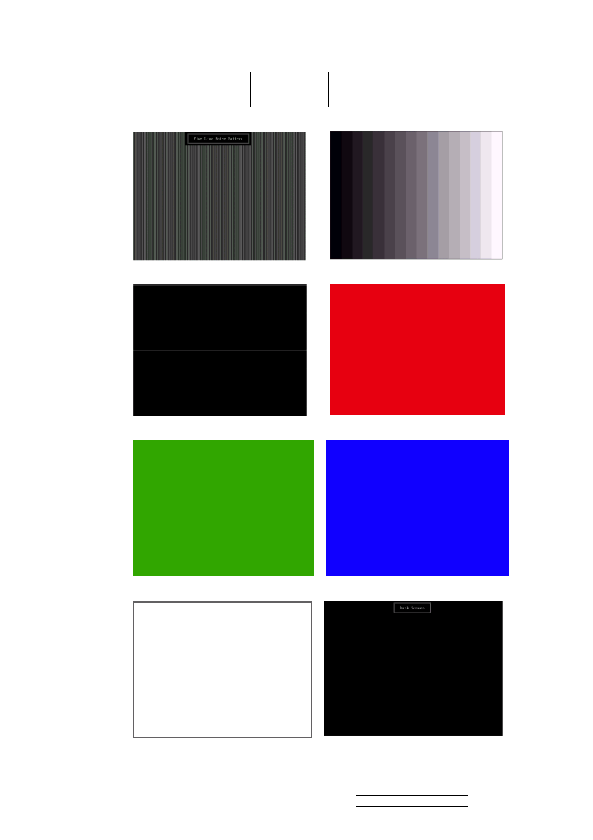
7 White Balance White & Black
Pattern
Fine Line Morie Pattern (Figure1) Gray Scale Pattern (Figure2)
The screen must have the pure
white and black pattern, no other
color.
Figure 9
Horizontal & Vertical Thickness Pattern (Figure 3) R. Color Pattern (Figure 4)
G. Color Pattern (Figure5) B. Color Pattern (Figure 6)
Full White Patter (Figure 7) Dark Screen Pattern (Figure 8)
ViewSonic Corporation Confidential - Do Not Copy Q9b-3
18

Black-White Pattern (Figure 9)
1.5. Function Test and Alignment Procedure
1.5.1 All Modes Reset
You should do “Memory Recall” (Refer to Chapter III-3. Hot Keys for Function
Controls) first. This action will allow you to erase all end-user’s settings and restore the
factory defaults.
1.5.2 Auto Image Adjust
Please select and enter “Auto Adjust” function on Main Menu to see if it is workable.
The “Auto Adjust” function is aimed to offer a better screen quality by built-in ASIC.
For optimum screen quality, the user has to adjust each function manually.
1.5.3 Firmware
Test Pattern: Burn In Mode (Refer to Chapter III-3. Hot Keys for Function Controls)
- Make sure the F/W is the latest version.
1.5.4 DDC
Test Pattern: EDID program
- Make sure it can pass test program.
1.5.5 Fine Tune and Sharpness
Test Signal: 1280*1024@60Hz
Test Pattern: Line Moire Pattern
- Check and see if the image has noise and focus performs well. Eliminate visual line
bar.
- If not, readjust by the following steps:
(a) Select and enter “Fine Tune” function on “Image Adjust” to adjust the image to
eliminate visual wavy noise.
(b) Then, select and enter “Sharpness” function to adjust the clarity and focus of the
screen image.
1.5.6 Boundary
Test Signal: 1280*1024@60Hz
Test Pattern: Horizontal & Vertical Line Thickness Pattern
- Check and see if the image boundary is within the screen frame.
- If not, readjust by the following steps:
(a) Select and enter “Image Adjust” function on OSD Main Menu.
ViewSonic Corporation Confidential - Do Not Copy Q9b-3
19

(b) Then, select and enter “H. Size” or “H./V. Position” function to adjust the video
boundary to be full scanned and within screen frame.
1.5.7 White Balance
A. TIMING: 1280x1024 64KHz/60Hz.
B. PATTERN: 5 Blocks.
C. LCD MONITOR set to 1280x1024 80K/75Hz BURN IN and warm up over 30
minutes.
D. CA110 color analizer at the center of screen and along a perpendicular to the
screen at 20cm from the display.
E. Power turn off, Press
power LED is on, release
factory mode. (Fig.1)
“▲” and “ ”
“▲” and “ ”
2
and turn on power at the same time after
key, Then press “ ” key go to
2
1
(Fig.1)
F. Adjust Color Temperature:
(1) EEPROM INIT (5 BLOCKS):
Press “▼” key move cursor to EEPROM INIT, Press “ ” key then
monitor will INIT ADC value.
(2) Press “▲” key move cursor to “White Balance”, Press “ ” key do
white balance adjustment.
(3) Press “▼” key move cursor to “Color Temperature Adjust”, Press
“ ” key, Then OSD will display Fig.2
2
(Fig.2)
(4) 9300K verify: move cursor to 9300K Press “ ” key.
Press “▼”, “▲” key adjust R.G.B value
x=0.283 ± 0.02
y=0.298 ± 0.02
Press “ ”key return to Fig.2
1
2
2
2
ViewSonic Corporation Confidential - Do Not Copy Q9b-3
20

(5) 6500K verify: Repeat (4) press “▼”, “▲” move cursor to 6500K press
“ ” key
2
x=0.313 ± 0.02
y=0.329 ± 0.02
(6) 5400K verify: Repeat (4) press “▼”, “▲” move cursor to 5400K press
“ ” key
2
x=0.332 ± 0.02
y=0.348 ± 0.02
(7) Press “ ” key go back to Fig.2, Then press “ ” key return to Fig.1,
Power key OFF/ON quit factory mode.
G. Color Temperature Verify:
BRIGHTNESS MAX, CONTRAST MAX
9300K: x=0.283
6500K: x=0.313
5400K: x=0.332
H. Luminance Verify:
BRIGHTNESS MAX, CONTRAST MAX
HSD190ME13A10/A16: Luminance :240(min)
HSD190ME13A02 : Luminance: 200(min)
1.5.8 R, G, B, Colors Contrast
Test Signal: 1280*1024@60Hz
Test Pattern: R, G, B, Color Intensities Pattern and 16 Gray Scale Pattern
- Check and see if each color is normal and distinguishable.
- If not, please return the unit to repair area.
1.5.9 Screen Uniformity and Flicker
Test Signal: 1280*1024@60Hz
Test Pattern: Full White Pattern
- Check and see if it is in normal condition.
1.5.10 Dead Pixel and Line
Test Signal: 1280*1024@60Hz
Test Pattern: Dark and White Screen Pattern
- Check and see if there are dead pixels on LCD panel with shadow gauge and filter
film.
- The total numbers and distance of dead pixels should be compliant with the spec.
1.5.11 Mura
Test Pattern: White, RGB, Black, & Grey
Test Tool: 8% ND Filter
- Check if the Mura can pass 8% ND Filter.
1.5.13 Check for Secondary Display Modes
Test Signal:
Analog: 640*350@70Hz; 640*480@60HZ
720*400@70Hz; 800*600@60HZ/70HZ/75HZ
832*624@75Hz, 1024*768@60HZ/70HZ/75HZ
1280*1024@60/75Hz
- Normally when the primary mode 1280*1024@60Hz is well adjusted and compliant
with the specification, the secondary display modes will be great possible to be
compliant with the spec. But we still have to check with the general test pattern to
make sure every secondary is compliant with the specification.
± 0.02 y=0.298 ± 0.02
± 0.02 y=0.329 ± 0.02
± 0.02 y=0.348 ± 0.02
11
ViewSonic Corporation Confidential - Do Not Copy Q9b-3
21

2. Firmware Upgrade Procedure
When you receive the returned monitor, please check whether the firmware version is the
latest. If not, please do the following procedures to upgrade it to the latest version.
2.1. Equipment Needed
- Q9/b-3 Monitor
- Fixture for Firmware Upgrade
- VGA Cable
- PC (Personal Computer)
- LPT Cable
- Firmware Upgrade Program
- One additional monitor for checking the program execution
1.5.14 All Modes Reset
1.5.15 Power Off Monitor
After final QC step, we have to erase all saved changes again and restore the factory
defaults. You should do “All Mode Reset” again.
Turn off the monitor by pressing “Power” button.
Printer Por
t
PC
LPT Cable
Q9b-3
VGA Cable
ViewSonic Corporation Confidential - Do Not Copy Q9b-3
22

2.2. Setup Procedure
2.2.1 Connect P2 of Fixture with printer port of PC by LPT Cable.
2.2.2 Connect P1 of Fixture with Q9/B-3 Monitor by VGA Cable.
2.2.4 Connect Power Cord to Q9/b-3 Monitor.
2.2.5 Connect PC to the additional monitor.
2.3. ISP Download program procedure
2.3.1 Hardware Connect status:
2.3.2 Down load isp program
Step 1: Execute ISP.exe
Step 2: Select device type
Pressing the
the Pm25LV512 for this project.
button to select the type of the device, It need to be selected
ViewSonic Corporation Confidential - Do Not Copy Q9b-3
23

Step 3: Connect device
Then press the
connection successful : press the button
button to connect device.
Step 4: Read file
to continue;
(1)Press the button
to enter the read-file page.
ViewSonic Corporation Confidential - Do Not Copy Q9b-3
24

(2)Press the button
to select file (*.bin).
Step 5: Run
Pressing the
button to download the firmware.
Button to enter the auto-download page. Press
ViewSonic Corporation Confidential - Do Not Copy Q9b-3
25

Step 6: Download program finish
Pressing the
Trouble shooting:
If you find the status like the follow picture. Please check the following item.
a. The connecting status between PC and ISP board.
b. The connecting status between ISP status and Monitor.
Turn off the power of monitor (AC plug off ) and disconnect the D-Sub connector .
To connect the D-Sub connector and then turn on the power of monitor.(AC plug on)
Button to finish the download program procedure.
If the test result shows “passed,” it means the connection is well. If not (failed), it means
the connection has problems.Then you need to check the setup procedure or reboot the PC,
or simply use another PC to do the firmware upgrade.
ViewSonic Corporation Confidential - Do Not Copy Q9b-3
26

3. DDC Key In Procedure
Note:
1. Every time after replacing the main board, you have to do the DDC key in.
2. If you find the DDC does not conform to the monitor, you have to do the DDC key in.
3.1. Equipment Needed
- JT198NP4FD3 Monitor
- DDC Card
- PC
- RS232 cable
- Barcode Reader
- VGA Cable
Q9b-3 DDC Card PC
RS-232 Cable VGA Cable Barcode Reader
3.2. Setup Procedure
3.2.1 Connect VGA Card and DDC Card with RS-232 cable.
ViewSonic Corporation Confidential - Do Not Copy Q9b-3
27

3.2.2 Barcode Reader connect with keyboard and PC keyboard port.
3.2.3 Connect RS-232 Cable and JT198NP4FD3 with VGA Cable.
3.2.4 Connect Power Cord to JT198NP4FD3 Monitor.
3.3. DDC Key In Procedure
3.3.1 Run DDC.exe
3.3.2 Choose model number and conform the Time then Press “ENTER” key.
3.3.3 When appear the PIC “ choose DDC Card”, Press ALT+2 Enter DDC 2B test
interface.
Choose DDC Card
ViewSonic Corporation Confidential - Do Not Copy Q9b-3
28

3.3.4 Press F8 to choose corresponding model.DAT (Q9-3.DAT press “ENTER” key)
(The filename on this picture is a example only, the exact one, please refer to your model.)
3.3.5 Press F9 enter the download interface
ViewSonic Corporation Confidential - Do Not Copy Q9b-3
29

3.3.6 Key in the serial number or use the barcode reader to scan the barcode of the
monitor, and press “ENTER” key.
3.3.7 The successful picture is as follows. ”Compare EDID :OK! Press any key to
continue”.
ViewSonic Corporation Confidential - Do Not Copy Q9b-3
30

3.3.8 Let Q9-3 active then see the information in OSD, it shows ”Serial NO :
PPZ0517A3178”
(The Serial NO. provided above is a example only; the exact one, please refer to your monitor.)
3.4. Check Method
Use ViewSonic EDID Editor
ViewSonic Corporation Confidential - Do Not Copy Q9b-3
31

Connect the Q9-3 Monitor to PC with VGA Cable. Excute the EDID Editor, then Press
Ctrl+F5. If the DDC is correct, you can see the information as follow:
(The data on this picture is a example only; the exact one, please refer to your monitor.)
ViewSonic Corporation Confidential - Do Not Copy Q9b-3
32

Packing For Shipping And Disassembly Procedure
Packing For Shipping
1. Packing Procedure
1.1 Paste protection film to protect the monitor. (Figure 1)
1.2 Put the monitor in the PE bag and seal the bag with tape. (Figure 2/3)
1.3 Put the cushions on the monitor. (Figure 4)
1.4 Place the monitor into the carton and then put all the accessories into the carton. At last, close the
carton and seal it with tape. (Figure 5)
Figure 1
Figure 3
Figure 2
1.Power Cord 2.VGA Cable
3.Audio Cable
Figure 4
User’s Guide
Figure 5
ViewSonic Corporation Confidential - Do Not Copy Q9b-3
33

Disassembly Procedure
1. Disassembly of Stand unit from Monitor
1.1 Remove Dust Cover.
1.2 Remove Stand Unit.
Dust cover
ViewSonic Corporation Confidential - Do Not Copy Q9b-3
34

1.3 Unscrew 4 screws to remove Hinge.
2. Disassembly of Front Cover and Rear Cover
2.1 Unscrew two screws that secure Rear Cover to remove Front Cover.
Front Cover
ViewSonic Corporation Confidential - Do Not Copy Q9b-3
35

2.2 Unscrew 2 screws to remove Rear Cover.
Rear Cover
3. Disassembly of Main Board, Keypad Board and Panel Unit
3.1 Unscrew 6 screws to remove Shielding Plate.
Shielding Plate
ViewSonic Corporation Confidential - Do Not Copy Q9b-3
36

3.2. Unscrew 7 screws and disconnect the wires to remove Main Board.
3.3. Lay Panel Unit facedown and unscrew 4 screws on its right and left sides to remove Panel Unit
and Keypad Board.
Main Board
Panel Unit
Panel Bracket
Keypad Board
ViewSonic Corporation Confidential - Do Not Copy Q9b-3
37

6. Troubleshooting Flow Chart
START
CHECK
MAIN
5V OK?
Y
3.3V OK?
Y
1.8V OK?
N
CHECK
POWER PCB
N
CHECK
D807,I801,I801
I104,SUROUND CAP
N
CHECK
D807,I801,I801
Q107,SUROUND CAP
OK?
OK?
Y
SUROUND CAP OK?
Y
SUROUND CAP OK?
Y
CHECK
Q107 1.8V
CHECK
AND I104,D130
CHECK
I104 3.3V
OK?
ViewSonic Corporation Confidential - Do Not Copy Q9b-3
38
SUROUND CAP OK?

6.1. NO POWER
Y
Y
POWER
STAR
Check
V 0/P
12
C823
Check F801
D801
C805
Check
I801
Q801
12V
Check
5 V O/P
T801
Check
D823
D822
5V
12V
Check
I902
Check
P901-P904
Check I901
Q905,Q911
Q907,Q908
Q909,Q910
Check
T902
T901
,
MAIN
PCB
PANEL
PA
ViewSonic Corporation Confidential - Do Not Copy Q9b-3
39

6.2. NO DISPLAY
Power key Check
Work ok Keypad
Y
Check Check
H V sync I105
Y
Check R.G.B Check
DATA I/O cable
Y
Check Check
X101
Y
Check I101 Check
HS,VS
HWRESET
Y
Y
Check
BACKLITE
N Check
N Check
C129,C130
SCL,SDA
Check
Q104
Check
5V
Check
P102
Check N Check
I105
Check N Check NN
I105,I104
Check N Check NN
SCL,SDA
I104,
Check N Check NN
NN
NN
NN
I107,
I104
I/O cable
P102
VCC1.8V,3.3v
SCL,SDA
PANEL P102 WIRE
ViewSonic Corporation Confidential - Do Not Copy Q9b-3
40

6.3. LOSE COLOR
Some bits
lost
Y
Check I105
N
I105 OR
R-pack
soldering
I107 poor
soldering
Lose color
R or G or B
Y
Check N
P107
Y
Check
R104,R105.R106
R108,R109,R110
Y
I105
fail or
Poor,,soldering
Sign
N
Check
C101,C102
C103,C107
C105,C106
Check
Sign Cable
ViewSonic Corporation Confidential - Do Not Copy Q9b-3
41

6.4. NO AUDIO
N
N
N
Check Jack
Check
12 V
Check
Audio cable
Check 12V
TRACE
Check
I601
Check
speaker
Check
P601
ViewSonic Corporation Confidential - Do Not Copy Q9b-3
42

7. Recommended Spare Parts List
ViewSonic Model Number: VS11455
Serial No. Prefix: QD8 Rev: 1a
Item ECR/ECN ViewSonic P/N Ref. P/N Location Universal number#
1
Accessories:
2
PC Board Assembly:
3
4
Cabinets:
5
6
7
8
9
10
Cables:
11
12
Documentation:
13
14
Electronic
15
Components:
16
17
Packing Material:
18
19
20
21
22
23
Plastics:
24
Remark 1:
Remark 2:
Description
Power Cord (German) 1.83M A-00006133 2427130047P P951
Main Board B-00008067 6201-7998344F31
Power Supply Board B-00008068 6202-7998344F31
Neck 178 W/Arm Up ABS 94HB C-00003192 2028553002 5B01
Neck 178 W/Arm Up ABS 94HB RoHS C-00008093 2028553002P 5B01
Neck 178 W/ Arm Down ABS 94HB C-00003195 2028553102 5B04
Neck 178 W/ Arm Down ABS 94HB RoHS C-00008094 2028553102P 5B04
Front Panel C-00008091 2603308070
Back Cover C-00008092 2603407714
I/O CABLE CB-00003009 2427501191P P961
Cable - (Ear 3.5 1.8M) CB-00005735 2427721841P P962
Quick Start Guide DC-00008082 2002370048P 6P84
CD-Rom DC-00008083 2438570036P 6P80
LCD Panel - HSD190ME13-A02 E-00003479 2212007901P V901
Speaker (Right) E-00008049 2391301098P W601
Speaker (Left) E-00008050 2391301099P W602
POLYETHY BAG M-MS-0808-1316 2013222536P 6P75
POLYETHY BAG M-MS-0808-1317 2013053000P 6P60
Craft Box P-00008075 2011020070P 6P01
Foam (Right) P-00008076 2012189500P 6P20
Foam (Left) P-00008077 2012189600P 6P21
POLYETHY BAG P-00008078 2013228805P 6P85
Pedestal (JT198DP) Black PL-00003187 2028258702 5B08
Pedestal (JT198DP) Black RoHS PL-00008023 2028258702P 5B08
Above listed items are examples, supplier can expand the rows to add more necessary items.
All revised RSPLs with newly added items or any change made should be highlighted and correlated with the ECN/ECR approved by
RECOMMENDED SPARE PARTS LIST (Q9b-3)
ViewSonic Corporation. This is to eliminate repeated cross checks of each item between this version and prior versions.
ViewSonic Corporation Confidential - Do Not Copy Q9b-3
43

BOM LIST (Q9b-3)
ViewSonic Model Number: VS11455
Rev: 1a
Serial No. Prefix: QD8
Item ViewSonic P/N Ref. P/N Description Location Universal number# Q'ty
1 N/A 2024273702P FRONT BEZEL JT198N ABS 94HB BLACK C 1F01 1
2 N/A 2053756201P LED INDIC.-PWR JT198N/PMMA 94HB 1F02 1
3 N/A 2044268003P FUNCTION KEY VP920/ABS 94HB BLACK C 1F03 1
4 N/A 2022267202P CABI BACK JT198V ABS HB BLACK C-F AUDIO 2C01 1
5 M-BK-0805-0070 2071869400P BRACKET,FIX METAL PLATE 1.0MM KENSINGTON 2C02 1
6 HW-00003031 2071872900P BRACKET,FIX JT198QP SECC 0.8T WALL MOUNT 2C03 1
7 N/A 2061254400P SPONGE SPONG BLK 50*20*3.0T 2C06 1
8 N/A 2061254400P SPONGE SPONG BLK 50*20*3.0T 2C07 1
9 C-00008093 2028553002P NECK 178W/ARM UP ABS 94HB BLACK C 5B01 1
10 N/A 2106656900P HINGE JT198QP -1'~20' 5B02 1
11 N/A 2106656901P HINGE JT198QP 0'~20' H.Y 5B02 1
12 N/A 2084740122P SCREW,BND T+ M4*12 (BND T+) 5B03 4
13 C-00008094 2028553102P NECK 178W/ARM DOWN ABS 94HB BLACK C 5B04 1
14 N/A 2105251800P SPRING PLATE JT178WP/EMI PLATE 5B05 1
15 M-SCW-0824-0812 2084730062P SCREW,BND T+ M3X6(BND T+) 5B06 1
16 N/A 2084740122P SCREW,BND T+ M4*12 (BND T+) 5B07 4
17 N/A 2028258702P STAND JT198DP ABS94HB #4001 BLACK 5B08 1
18 N/A 2071973400P METAL FITTG JT198DP SECC 1.0T STAND 5B09 1
19 M-SCW-0824-0812 2084730062P SCREW,BND T+ M3X6(BND T+) 5B10 4
20 PL-PD-0714-0113 2039819301P FOOT PAD RUBBER O20*2TMM SQUARE GRAIN 5B11 4
21 N/A 2055690057P LABEL JT198NP4FD3 Q9b STAND INSTALL 5B12 1
22 N/A 2071979500P METAL FITTG JT198V SECC 0.6T F 5F01 1
23 N/A 2080002200P SCREW,SPE L355 M3x6 DH NICKEL-PLATED 5F02 4
24 N/A 2082630064P SCREW M3*6 P=0.5 BLACK 6B01 4
25 N/A 2084730104P SCREW,BND T+ M3X10(BND T+)BLACK 6B02 2
26 N/A 2086240132P SCREW,P SW+ M4*12 PSW+ 2N 6B03 4
27 N/A 2027258102P DUST COVER JT178WP/ABS 94HB BLACK C 6B04 1
28 M-SCW-0824-0285 2084730082P SCREW,BND T+ M3X8(BND T+) 6B05 2
29 N/A 2082630064P SCREW M3*6 P=0.5 BLACK 6B06 2
30 M-SCW-0824-0811 2080003700P SCREW,SPE ISZZTER001A M3*6L MSWR17/FZMYI 6F01 6
31 N/A 2081440082P SCREW,(WASH) M4X8 P=0.7(TOOTH WASHER) 6F04 1
32 N/A 2071678800P SHIELD PLATE JT198V SPTE 0.3T F-PHONE 6F05 1
33 N/A 2082630042P SCREW M3*4 P=0.5 6F06 3
34 HW-00003028 2071874300P BRACKET,FIX SECC T=0.8 VE910 ACINLET 6F11 1
35 P-00008075 2011020070P CARTON BOX JT198NP4FD3 Q9b VS11455 WW 6P01 1
36 N/A 2055670103P LABEL JT198NP4FD3 Q9b-3 VS11455 (E) 6P02 1
37 N/A 2055690060P LABEL ENERGYSTAR LABEL 11X11MM NO PP 6P03 1
38 N/A 2055690056P LABEL Q9b-3 VS11455 SMALL LABEL 6P05 1
39 N/A 2055613379P LABEL VIEWSONIC CONTAINER LABEL 6P11 25
40 M-LB-0813-0530 2055617101P LABEL 10*20 HI-POT TESTED OK 6P13 1
41 M-LB-0813-0959 2055613392P LABEL VSC HIGH VOLTAGE WARNING LABEL 6P14 1
42 P-00008076 2012189500P POLYFOAM JT198N-X,D/EPS (R) 6P20 1
43 P-00008077 2012189600P POLYFOAM JT198N-X D/EPS (L) 6P21 1
44 N/A 2055170164P LABEL JT198NP4FD3 Q9b VS11455 TCO99 6P50 1
45 M-MS-0808-1317 2013053000P POLYETHY BAG 90CMX75CMX0.02t PE-LD 6P60 1
46 M-MS-0808-1316 2013222536P POLYETHY BAG 250mmX350mmX0.3t ADD>PE-LD< 6P75 1
47 DC-00008083 2438570036P CD-OWNER GUIDE Q9b-3 WIZARD CD HSD 6P80 1
48 DC-00008082 2002370048P GUARANT CARD VIEWSONIC Q9b-3 QSG 6P84 1
49 P-00008078 2013228805P POLYETHY BAG 175X280X0.03T mm LDPE A5 6P85 1
50 N/A 2072253903P HEAT SINK JT178DP SPTE T=1MM 9H01 1
51 N/A 2072261500P HEAT SINK JT178DP 40L*35W*20H AL T=3 9H02 1
52 N/A 2072261401P HEAT SINK JT178QP AL6063S-75 30*20*15 9H03 1
53 N/A 2105251400P SPRING PLATE SPTE T=0.4MM (GROUND PLATE) 9H11 1
54 N/A 2105251400P SPRING PLATE SPTE T=0.4MM (GROUND PLATE) 9H12 1
55 N/A 2105251400P SPRING PLATE SPTE T=0.4MM (GROUND PLATE) 9H13 1
56 M-SCW-0824-0285 2084730082P SCREW,BND T+ M3X8(BND T+) 9S01 1
57 M-SCW-0824-0285 2084730082P SCREW,BND T+ M3X8(BND T+) 9S02 1
58 M-SCW-0824-0285 2084730082P SCREW,BND T+ M3X8(BND T+) 9S03 1
59 N/A 2281447391P CAP CER CC 0.047u/ 50V Y5V P=5.0 Z T C101 1
60 N/A 2281447391P CAP CER CC 0.047u/ 50V Y5V P=5.0 Z T C102 1
61 N/A 2281447391P CAP CER CC 0.047u/ 50V Y5V P=5.0 Z T C103 1
62 N/A 2281447391P CAP CER CC 0.047u/ 50V Y5V P=5.0 Z T C105 1
63 N/A 2281447391P CAP CER CC 0.047u/ 50V Y5V P=5.0 Z T C106 1
64 N/A 2281447391P CAP CER CC 0.047u/ 50V Y5V P=5.0 Z T C107 1
65 E-C-0404-1815 2281410491P CAP CER CC 0.1u/ 50V Y5V P=5.0 Z T C116 1
66 N/A 2333347691P CAP ELE 105'C EC 47u/ 16V 5*11 P=5.0 T C117 1
67 N/A 2333347691P CAP ELE 105'C EC 47u/ 16V 5*11 P=5.0 T C119 1
68 E-C-0404-1815 2281410491P CAP CER CC 0.1u/ 50V Y5V P=5.0 Z T C120 1
69 E-C-0404-1834 2333647591P CAP ELE 105'C EC 4.7u/ 50V 5*11 P=5.0 T C124 1
70 E-C-0404-1424 2333610591P CAP ELE 105'C EC 1u/ 50V 5*11 P=5.0 T C125 1
71 E-C-0404-1815 2281410491P CAP CER CC 0.1u/ 50V Y5V P=5.0 Z T C126 1
72 E-C-0404-1815 2281410491P CAP CER CC 0.1u/ 50V Y5V P=5.0 Z T C127 1
73 E-C-0404-1838 2333610691P CAP ELE 105'C EC 10u/ 50V 5*11 P=5.0 T C128 1
74 N/A 2272122091P CAP CER TC 22p/50V CH P=5.0 J T C129 1
75 N/A 2272122091P CAP CER TC 22p/50V CH P=5.0 J T C130 1
76 E-C-0404-1815 2281410491P CAP CER CC 0.1u/ 50V Y5V P=5.0 Z T C131 1
77 E-C-0404-1815 2281410491P CAP CER CC 0.1u/ 50V Y5V P=5.0 Z T C132 1
78 E-C-0404-1834 2333647591P CAP ELE 105'C EC 4.7u/ 50V 5*11 P=5.0 T C134 1
ViewSonic Corporation Confidential - Do Not Copy Q9b-3
44

Item ViewSonic P/N Ref. P/N Description Location Universal number# Q'ty
79 N/A 2281410401P CAP CER CC 0.1u/ 50V Y5V P=5.0 Z T C135 1
80 N/A 2281410401P CAP CER CC 0.1u/ 50V Y5V P=5.0 Z T C136 1
81 E-C-0404-1815 2281410491P CAP CER CC 0.1u/ 50V Y5V P=5.0 Z T C137 1
82 E-C-0404-1838 2333610691P CAP ELE 105'C EC 10u/ 50V 5*11 P=5.0 T C138 1
83 E-C-0404-1815 2281410491P CAP CER CC 0.1u/ 50V Y5V P=5.0 Z T C139 1
84 E-C-0404-1119 2272122191P CAP CER TC 220p/50V CH P=5.0 J T C140 1
85 N/A 2272122091P CAP CER TC 22p/50V CH P=5.0 J T C141 1
86 N/A 2333610601P CAP,ELE 105'C EC 10u/ 50V 5*11 P=2.0 C C142 1
87 E-C-0404-1815 2281410491P CAP CER CC 0.1u/ 50V Y5V P=5.0 Z T C143 1
88 N/A 2281410401P CAP CER CC 0.1u/ 50V Y5V P=5.0 Z T C144 1
89 E-C-0404-1815 2281410491P CAP CER CC 0.1u/ 50V Y5V P=5.0 Z T C145 1
90 E-C-0404-1838 2333610691P CAP ELE 105'C EC 10u/ 50V 5*11 P=5.0 T C146 1
91 E-C-0404-1815 2281410491P CAP CER CC 0.1u/ 50V Y5V P=5.0 Z T C148 1
92 E-C-0404-1838 2333610691P CAP ELE 105'C EC 10u/ 50V 5*11 P=5.0 T C149 1
93 E-C-0404-1815 2281410491P CAP CER CC 0.1u/ 50V Y5V P=5.0 Z T C150 1
94 E-C-0404-1838 2333610691P CAP ELE 105'C EC 10u/ 50V 5*11 P=5.0 T C151 1
95 N/A 2281410401P CAP CER CC 0.1u/ 50V Y5V P=5.0 Z T C153 1
96 N/A 2333347691P CAP ELE 105'C EC 47u/ 16V 5*11 P=5.0 T C156 1
97 N/A 2333347691P CAP ELE 105'C EC 47u/ 16V 5*11 P=5.0 T C157 1
98 E-C-0404-2271 2333310791P CAP ELE 105'C EC 100u/ 16V 6.3*11 P=5.0 T C168 1
99 E-C-0404-1815 2281410491P CAP CER CC 0.1u/ 50V Y5V P=5.0 Z T C169 1
100 E-C-0404-1838 2333610691P CAP ELE 105'C EC 10u/ 50V 5*11 P=5.0 T C172 1
101 N/A 2333310812P CAP ELE 105'C EC 1000u/ 16V10*17 P=5.0 K C601 1
102 N/A 2333322691P CAP,ELE 105'C EC 22u/ 16V 5*11 P=5.0 T C602 1
103 E-C-0404-1424 2333610591P CAP ELE 105'C EC 1u/ 50V 5*11 P=5.0 T C603 1
104 E-C-0404-1424 2333610591P CAP ELE 105'C EC 1u/ 50V 5*11 P=5.0 T C604 1
105 N/A 2333347791P CAP ELE 105'C EC 470u/ 16V 10*12.5 P=5.0 T C605 1
106 N/A 2333347791P CAP ELE 105'C EC 470u/ 16V 10*12.5 P=5.0 T C606 1
107 N/A 2333322791P CAP ELE 105'C EC 220u/ 16V 8*11 P=5.0 T C610 1
108 E-C-0404-1815 2281410491P CAP CER CC 0.1u/ 50V Y5V P=5.0 Z T C615 1
109 N/A 2300947401P CAP,MTL MINI X2 0.47u/275V P=15.0 M C C801 1
110 E-00005729 2300947481P X CAP MINI X2 0.47u/275V P=15.0 K C C801 1
111 E-C-0404-1855 2287247212P CAP CER Y2 4700p/250V Y5V P=10.0 M K C802 1
112 E-C-0404-1855 2287247212P CAP CER Y2 4700p/250V Y5V P=10.0 M K C803 1
113 N/A 2357510708P EC HI-RIPPLE 105C 400V EC 100u/400V 18*32 P=7.5 S C805 1
114 E-C-0404-2262 2285110291P CAP CER CC 1000P/1KV Y5P P=5.0 K T C806 1
115 N/A 2281147191P CAP CER CC 470pF/50V P=5.0 K T C808 1
116 E-C-0404-1838 2333610691P CAP ELE 105'C EC 10u/ 50V 5*11 P=5.0 T C810 1
117 N/A 2283322291P CAP CER 125'C CC 2200p/500V X7R P=5.0 K T C820 1
118 N/A 2283322291P CAP CER 125'C CC 2200p/500V X7R P=5.0 K T C821 1
119 N/A 2336010811P HI-LIFE LOW ESR ELE CAP EC 1000u/ 16V 10*16 P=5.0 C C822 1
120 N/A 2330006491P CAP ELE SPECIAL (3000HR) EC 470u /16V 10*13 P=5.0 T C823 1
121 N/A 2336010801P HI-LIFE LOW ESR ELE CAP EC 1000u/ 10V 8*20 P=3.5 C C824 1
122 N/A 2335347773P CAP,ELE LOW ESR 105'C (6 000HR) EC 470u/ 16V 10*13 P=5.0 T C825 1
123 N/A 2281110491P CAP CER CC 0.1u/50V (Y5P) P=5.0 K T C826 1
124 E-C-0404-1838 2333610691P CAP ELE 105'C EC 10u/ 50V 5*11 P=5.0 T C827 1
125 N/A 2285122191P CAP CER CC 220P/1KV Y5P P=5.0 K T C828 1
126 N/A 2335310841P CAP,ELE LOW ESR 105'C EC 1000u/ 16V 10*16 P=5.0 C C829 1
127 N/A 2287210300P CAP CER Y2 0.01uF/250V P=10.0 M C831 1
128 N/A 2302047391P CAP,MTL MEF 0.047uF/50V P=5.0 J T C901 1
129 N/A 2275422001P CAP CER TC 22P/3KV SL P=7.5 J C C902 1
130 E-00005730 2284022291P CAP CER CC 2200p/50V X7R P=5.0 K T C903 1
131 E-00005730 2284022291P CAP CER CC 2200p/50V X7R P=5.0 K T C904 1
132 N/A 2275450901P CAP CER TC 5P/3KV SL P=7.5 J C C905 1
133 N/A 2330006491P CAP ELE SPECIAL (3000HR) EC 470u /16V 10*13 P=5.0 T C906 1
134 E-00003555 2302047291P CAP,MTL MEF 4700pF/50V P=5.0 J T C908 1
135 N/A 2284010391P CAP CER CC 0.01u/50V X7R P=5.0 K T C910 1
136 N/A 2281110491P CAP CER CC 0.1u/50V (Y5P) P=5.0 K T C911 1
137 N/A 2284010391P CAP CER CC 0.01u/50V X7R P=5.0 K T C912 1
138 N/A 2284010391P CAP CER CC 0.01u/50V X7R P=5.0 K T C913 1
139 N/A 2281110491P CAP CER CC 0.1u/50V (Y5P) P=5.0 K T C914 1
140 N/A 2275422001P CAP CER TC 22P/3KV SL P=7.5 J C C916 1
141 N/A 2284010291P CAP CER CC 1000p/50V X7R P=5.0 K T C917 1
142 N/A 2275450901P CAP CER TC 5P/3KV SL P=7.5 J C C918 1
143 E-00003555 2302047291P CAP,MTL MEF 4700pF/50V P=5.0 J T C919 1
144 N/A 2330006491P CAP ELE SPECIAL (3000HR) EC 470u /16V 10*13 P=5.0 T C922 1
145 N/A 2302068391P CAP,MTL MEF 0.068u/50V P=5.0 J T C924 1
146 N/A 2281110491P CAP CER CC 0.1u/50V (Y5P) P=5.0 K T C925 1
147 E-00005730 2284022291P CAP CER CC 2200p/50V X7R P=5.0 K T C926 1
148 E-00005730 2284022291P CAP CER CC 2200p/50V X7R P=5.0 K T C927 1
149 N/A 2281110491P CAP CER CC 0.1u/50V (Y5P) P=5.0 K T C928 1
150 E-D-0403-0531 2363600195P DIODE,SWITCH 1N4148 DO-35 WILLAS D101 1
151 N/A 2363601795P DIODE,SWITCH 1N4148TA_NL DO-35 FAIRCHILD D101 1
152 N/A 2363601895P DIODE,SWITCH 1N4148 DO-35 TSC D101 1
153 E-D-0403-0531 2363600195P DIODE,SWITCH 1N4148 DO-35 WILLAS D102 1
154 N/A 2363601795P DIODE,SWITCH 1N4148TA_NL DO-35 FAIRCHILD D102 1
155 N/A 2363601895P DIODE,SWITCH 1N4148 DO-35 TSC D102 1
156 E-D-0403-0531 2363600195P DIODE,SWITCH 1N4148 DO-35 WILLAS D103 1
157 N/A 2363601795P DIODE,SWITCH 1N4148TA_NL DO-35 FAIRCHILD D103 1
158 N/A 2363601895P DIODE,SWITCH 1N4148 DO-35 TSC D103 1
159 E-D-0403-0531 2363600195P DIODE,SWITCH 1N4148 DO-35 WILLAS D104 1
160 N/A 2363601795P DIODE,SWITCH 1N4148TA_NL DO-35 FAIRCHILD D104 1
161 N/A 2363601895P DIODE,SWITCH 1N4148 DO-35 TSC D104 1
ViewSonic Corporation Confidential - Do Not Copy Q9b-3
45

Item ViewSonic P/N Ref. P/N Description Location Universal number# Q'ty
162 E-D-0403-0531 2363600195P DIODE,SWITCH 1N4148 DO-35 WILLAS D105 1
163 N/A 2363601795P DIODE,SWITCH 1N4148TA_NL DO-35 FAIRCHILD D105 1
164 N/A 2363601895P DIODE,SWITCH 1N4148 DO-35 TSC D105 1
165 E-D-0403-0531 2363600195P DIODE,SWITCH 1N4148 DO-35 WILLAS D106 1
166 N/A 2363601795P DIODE,SWITCH 1N4148TA_NL DO-35 FAIRCHILD D106 1
167 N/A 2363601895P DIODE,SWITCH 1N4148 DO-35 TSC D106 1
168 N/A 2363516895P DIODE,ZENER HZ6B-2 5.6-5.9V DO-35 HITACHI D107 1
169 N/A 2363516895P DIODE,ZENER HZ6B-2 5.6-5.9V DO-35 HITACHI D108 1
170 N/A 2363516895P DIODE,ZENER HZ6B-2 5.6-5.9V DO-35 HITACHI D110 1
171 N/A 2363516895P DIODE,ZENER HZ6B-2 5.6-5.9V DO-35 HITACHI D111 1
172 E-D-0403-0531 2363600195P DIODE,SWITCH 1N4148 DO-35 WILLAS D124 1
173 N/A 2363601795P DIODE,SWITCH 1N4148TA_NL DO-35 FAIRCHILD D124 1
174 N/A 2363601895P DIODE,SWITCH 1N4148 DO-35 TSC D124 1
175 E-D-0403-0531 2363600195P DIODE,SWITCH 1N4148 DO-35 WILLAS D125 1
176 N/A 2363601795P DIODE,SWITCH 1N4148TA_NL DO-35 FAIRCHILD D125 1
177 N/A 2363601895P DIODE,SWITCH 1N4148 DO-35 TSC D125 1
178 N/A 2363516895P DIODE,ZENER HZ6B-2 5.6-5.9V DO-35 HITACHI D126 1
179 E-D-0403-0531 2363600195P DIODE,SWITCH 1N4148 DO-35 WILLAS D127 1
180 N/A 2363601795P DIODE,SWITCH 1N4148TA_NL DO-35 FAIRCHILD D127 1
181 N/A 2363601895P DIODE,SWITCH 1N4148 DO-35 TSC D127 1
182 N/A 2428106125P JUMPER ∮0.6*12.5mm
183 E-D-0403-1500 2363222195P DIODE,RECT SB140 DO-41 PEC D129 1
184 E-D-0403-1500 2363222195P DIODE,RECT SB140 DO-41 PEC D130 1
185 E-D-0403-0531 2363600195P DIODE,SWITCH 1N4148 DO-35 WILLAS D601 1
186 N/A 2363601795P DIODE,SWITCH 1N4148TA_NL DO-35 FAIRCHILD D601 1
187 N/A 2363601895P DIODE,SWITCH 1N4148 DO-35 TSC D601 1
188 N/A 2363703808P LED 3∮ GRN/YEL H=7.5mm D701 1
189 N/A 2368501800P RECT,BRIDGE 2KBP06M 600V/2A PEC D801 1
190 N/A 2368502800P RECT,BRIDGE 2KBP06M(LF) 600V/2A MOSPEC D801 1
191 N/A 2363231995P DIODE,RECT UF4007 DO-41 1000V/1A PEC D806 1
192 N/A 2363234995P DIODE,RECT UF4007 DO-41 MOSPEC D806 1
193 E-D-0403-1465 2363220395P DIODE,RECT UF4004G DO-41 PEC D807 1
194 N/A 2363235195P DIODE,RECT UPG10G DO-204AL ZOWIE D807 1
195 N/A 2363303900P DIODE,SCHOTTKY GMR10H125C TO-220AB GAMMA D821 1
196 N/A 2363303700P DIODE,SCHOTTKY GMR10H100C TO-220AB GAMMA D821 1
197 N/A 2363303300P DIODE,SCHOTTKY FCH10U10 TO-220AB NI D821 1
198 N/A 2363300212P DIODE,SCHOTTKY 31DQ06FC 60V/1.6A H=21.4 NI D822 1
199 N/A 2363234012P DIODE,RECT SR306(LF) DO-201AD MOSPEC D822 1
200 N/A 2363300212P DIODE,SCHOTTKY 31DQ06FC 60V/1.6A H=21.4 NI D823 1
201 N/A 2363234012P DIODE,RECT SR306(LF) DO-201AD MOSPEC D823 1
202 N/A 2428106075P JUMPER 0.6∮*7.5mm
203 E-D-0403-0531 2363600195P DIODE,SWITCH 1N4148 DO-35 WILLAS D902 1
204 N/A 2363601795P DIODE,SWITCH 1N4148TA_NL DO-35 FAIRCHILD D902 1
205 N/A 2363601895P DIODE,SWITCH 1N4148 DO-35 TSC D902 1
206 E-D-0403-0531 2363600195P DIODE,SWITCH 1N4148 DO-35 WILLAS D905 1
207 N/A 2363601795P DIODE,SWITCH 1N4148TA_NL DO-35 FAIRCHILD D905 1
208 N/A 2363601895P DIODE,SWITCH 1N4148 DO-35 TSC D905 1
209 E-D-0403-0531 2363600195P DIODE,SWITCH 1N4148 DO-35 WILLAS D906 1
210 N/A 2363601795P DIODE,SWITCH 1N4148TA_NL DO-35 FAIRCHILD D906 1
211 N/A 2363601895P DIODE,SWITCH 1N4148 DO-35 TSC D906 1
212 E-D-0403-0531 2363600195P DIODE,SWITCH 1N4148 DO-35 WILLAS D907 1
213 N/A 2363601795P DIODE,SWITCH 1N4148TA_NL DO-35 FAIRCHILD D907 1
214 N/A 2363601895P DIODE,SWITCH 1N4148 DO-35 TSC D907 1
215 E-D-0403-0531 2363600195P DIODE,SWITCH 1N4148 DO-35 WILLAS D908 1
216 N/A 2363601795P DIODE,SWITCH 1N4148TA_NL DO-35 FAIRCHILD D908 1
217 N/A 2363601895P DIODE,SWITCH 1N4148 DO-35 TSC D908 1
218 E-D-0403-0531 2363600195P DIODE,SWITCH 1N4148 DO-35 WILLAS D909 1
219 N/A 2363601795P DIODE,SWITCH 1N4148TA_NL DO-35 FAIRCHILD D909 1
220 N/A 2363601895P DIODE,SWITCH 1N4148 DO-35 TSC D909 1
221 E-D-0403-0531 2363600195P DIODE,SWITCH 1N4148 DO-35 WILLAS D910 1
222 N/A 2363601795P DIODE,SWITCH 1N4148TA_NL DO-35 FAIRCHILD D910 1
223 N/A 2363601895P DIODE,SWITCH 1N4148 DO-35 TSC D910 1
224 E-D-0403-0531 2363600195P DIODE,SWITCH 1N4148 DO-35 WILLAS D911 1
225 N/A 2363601795P DIODE,SWITCH 1N4148TA_NL DO-35 FAIRCHILD D911 1
226 N/A 2363601895P DIODE,SWITCH 1N4148 DO-35 TSC D911 1
227 E-D-0403-0531 2363600195P DIODE,SWITCH 1N4148 DO-35 WILLAS D912 1
228 N/A 2363601795P DIODE,SWITCH 1N4148TA_NL DO-35 FAIRCHILD D912 1
229 N/A 2363601895P DIODE,SWITCH 1N4148 DO-35 TSC D912 1
230 E-D-0403-0531 2363600195P DIODE,SWITCH 1N4148 DO-35 WILLAS D913 1
231 N/A 2363601795P DIODE,SWITCH 1N4148TA_NL DO-35 FAIRCHILD D913 1
232 N/A 2363601895P DIODE,SWITCH 1N4148 DO-35 TSC D913 1
233 E-D-0403-0531 2363600195P DIODE,SWITCH 1N4148 DO-35 WILLAS D915 1
234 N/A 2363601795P DIODE,SWITCH 1N4148TA_NL DO-35 FAIRCHILD D915 1
235 N/A 2363601895P DIODE,SWITCH 1N4148 DO-35 TSC D915 1
236 E-D-0403-0531 2363600195P DIODE,SWITCH 1N4148 DO-35 WILLAS D916 1
237 N/A 2363601795P DIODE,SWITCH 1N4148TA_NL DO-35 FAIRCHILD D916 1
238 N/A 2363601895P DIODE,SWITCH 1N4148 DO-35 TSC D916 1
239 E-D-0403-0531 2363600195P DIODE,SWITCH 1N4148 DO-35 WILLAS D917 1
240 N/A 2363601795P DIODE,SWITCH 1N4148TA_NL DO-35 FAIRCHILD D917 1
241 N/A 2363601895P DIODE,SWITCH 1N4148 DO-35 TSC D917 1
242 E-D-0403-0531 2363600195P DIODE,SWITCH 1N4148 DO-35 WILLAS D918 1
243 N/A 2363601795P DIODE,SWITCH 1N4148TA_NL DO-35 FAIRCHILD D918 1
244 N/A 2363601895P DIODE,SWITCH 1N4148 DO-35 TSC D918 1
D128
D901
1
1
ViewSonic Corporation Confidential - Do Not Copy Q9b-3
46

Item ViewSonic P/N Ref. P/N Description Location Universal number# Q'ty
245 E-D-0403-0531 2363600195P DIODE,SWITCH 1N4148 DO-35 WILLAS D919 1
246 N/A 2363601795P DIODE,SWITCH 1N4148TA_NL DO-35 FAIRCHILD D919 1
247 N/A 2363601895P DIODE,SWITCH 1N4148 DO-35 TSC D919 1
248 E-FS-0410-0009 2213125207P FUSE 21502.5(2.5A) LITTEL F801 1
249 N/A 2213125211P FUSE FUSE 2.5A/250V SG501302.5 PICO F801 1
250 M-WR-0828-0460 2428106125P JUMPER ∮0.6*12.5mm
251 N/A 2365335010P LINEAR IC AP1084T33L TO-220 Anachip I104 1
252 N/A 2365335060P LINEAR IC AIC1084-33PT TO-220 AIC I104 1
253 N/A 2365425216P DIGITAL IC TSUM16AK-LF PQFP-128 Mstar I105 1
254 N/A 2365106196P MEMORY IC (FLASH) PM25LV512SCE SO-8 PMC I106 RA 1
255 N/A 2365106696P MEMORY IC (FLASH) PS25LV512-33SCE SOIC-8 Mstar I106 RB 1
256 N/A 2365915896P IC,DIGITAL SMD 24LC16BT/SN SO-8 MICROCHIP I107 RA 1
257 N/A 2365100996P MEMORY IC AT24C16AN-10SU-2.7 SO-8 AMTEL I107 RB 1
258 N/A 2365106396P MEMORY IC (EEPROM) M24C16-WMN6TP SO-8 ST I107 RC 1
259 N/A 2365335280P LINEAR IC GMA7496L-D20 DIP-20 GAMMA I601 1
260 N/A 2365329700P LINEAR IC TDA7496L DIP-20 ST I601 1
261 N/A 2365335266P LINEAR IC LD7575PS SOP-8 Leadtrend I801 1
262 E-PC-0411-0083 2362401800P PHOTO COUPLR TLP621 TOSHIBA I802 1
263 E-00005306 2362402300P PHOTO COUPLR TLP421 DIP4 TOSHIBA I802 1
264 N/A 2365328191P LINEAR IC AP431VLA TO-92 ATC I803 1
265 E-IC-0401-1270 2365319391P LINEAR IC TL431CLPRE3 TO-92 TI I803 1
266 E-IC-0401-2152 2365321991P LINEAR IC KA431AZTA TO-92 FAIRCHILD I803 1
267 N/A 2365327691P LINEAR IC CM431GDCN TO-92 CHAMPION I803 1
268 N/A 2365335236P LINEAR IC OZ9936GN SOIC-8 O2-MICRO I901 1
269 N/A 2428106250P JUMPER 0.6φ25.00MM J102 1
270 N/A 2428106250P JUMPER 0.6φ25.00MM J103 1
271 N/A 2428106075P JUMPER 0.6∮*7.5mm
272 N/A 2428106075P JUMPER 0.6∮*7.5mm
273 N/A 2428106100P JUMPER 0.6∮*10.0mm
274 n/A 2428106125P JUMPER ∮0.6*12.5mm
275 N/A 2428106075P JUMPER 0.6∮*7.5mm
276 N/A 2428208125P WIRE,STRIP ∮0.8*12.5mm
277 N/A 2428106075P JUMPER 0.6∮*7.5mm
278 N/A 2428106125P JUMPER ∮0.6*12.5mm
279 N/A 2428106100P JUMPER 0.6∮*10.0mm
280 N/A 2428208100P WIRE,STRIP ∮0.8*10.0mm
281 N/A 2428208200P WIRE,STRIP ∮0.8*20.0mm
282 N/A 2428208050P WIRE,STRIP ∮0.8*5.0mm
283 N/A 2428106075P JUMPER 0.6∮*7.5mm
284 N/A 2428106075P JUMPER 0.6∮*7.5mm
285 M-WR-0828-0455 2428106050P JUMPER ∮0.6*5.0mm
286 M-WR-0828-0455 2428106050P JUMPER ∮0.6*5.0mm
287 M-WR-0828-0455 2428106050P JUMPER ∮0.6*5.0mm
288 M-WR-0828-0455 2428106050P JUMPER ∮0.6*5.0mm
289 M-WR-0828-0455 2428106050P JUMPER ∮0.6*5.0mm
290 N/A 2428208050P WIRE,STRIP ∮0.8*5.0mm
291 M-WR-0828-0455 2428106050P JUMPER ∮0.6*5.0mm
292 M-WR-0828-0455 2428106050P JUMPER ∮0.6*5.0mm
293 N/A 2428106075P JUMPER 0.6∮*7.5mm
294 M-WR-0828-0455 2428106050P JUMPER ∮0.6*5.0mm
295 N/A 2428106075P JUMPER 0.6∮*7.5mm
296 N/A 2428106075P JUMPER 0.6∮*7.5mm
297 M-WR-0828-0455 2428106050P JUMPER ∮0.6*5.0mm
298 N/A 2428106100P JUMPER 0.6∮*10.0mm
299 N/A 2428106100P JUMPER 0.6∮*10.0mm
300 N/A 2428106075P JUMPER 0.6∮*7.5mm
301 N/A 2428106100P JUMPER 0.6∮*10.0mm
302 N/A 2428106125P JUMPER ∮0.6*12.5mm
303 N/A 2428106075P JUMPER 0.6∮*7.5mm
304 N/A 2428106075P JUMPER 0.6∮*7.5mm
305 N/A 2428106075P JUMPER 0.6∮*7.5mm
306 M-WR-0828-0455 2428106050P JUMPER ∮0.6*5.0mm
307 N/A 2428106150P JUMPER 0.6∮*15.0mm
308 N/A 2428106075P JUMPER 0.6∮*7.5mm
309 N/A 2428106100P JUMPER 0.6∮*10.0mm
310 N/A 2428106075P JUMPER 0.6∮*7.5mm
311 N/A 2428106075P JUMPER 0.6∮*7.5mm
312 N/A 2428106075P JUMPER 0.6∮*7.5mm
313 M-WR-0828-0455 2428106050P JUMPER ∮0.6*5.0mm
314 N/A 2428106075P JUMPER 0.6∮*7.5mm
315 N/A 2428106075P JUMPER 0.6∮*7.5mm
316 N/A 2428106075P JUMPER 0.6∮*7.5mm
317 N/A 2428106075P JUMPER 0.6∮*7.5mm
318 N/A 2428106075P JUMPER 0.6∮*7.5mm
319 N/A 2428106075P JUMPER 0.6∮*7.5mm
320 N/A 2428106075P JUMPER 0.6∮*7.5mm
321 M-WR-0828-0455 2428106050P JUMPER ∮0.6*5.0mm
322 N/A 2428106075P JUMPER 0.6∮*7.5mm
323 N/A 2428106100P JUMPER 0.6∮*10.0mm
324 N/A 2233422095P RES,CBN 1/4 S RD 1/4WS 22 ohm J T52 J906 1
325 N/A 2233422095P RES,CBN 1/4 S RD 1/4WS 22 ohm J T52 J907 1
F802
J104
J105
J106
J107
J108
J109
J110
J111
J112
J113
J114
J115
J116
J117
J118
J119
J120
J121
J122
J123
J124
J125
J126
J127
J128
J129
J130
J131
J132
J133
J134
J135
J136
J137
J138
J139
J140
J141
J142
J601
J602
J603
J604
J805
J806
J807
J808
J809
J901
J902
J903
J904
J905
1
1
1
1
1
1
1
1
1
1
1
1
1
1
1
1
1
1
1
1
1
1
1
1
1
1
1
1
1
1
1
1
1
1
1
1
1
1
1
1
1
1
1
1
1
1
1
1
1
1
1
1
1
1
ViewSonic Corporation Confidential - Do Not Copy Q9b-3
47
Item ViewSonic P/N Ref. P/N Description Location Universal number# Q'ty
326 N/A 2428106200P JUMPER 0.6∮*20mm
327 N/A 2428106150P JUMPER 0.6∮*15.0mm
328 N/A 2428106175P JUMPER 0.6∮*17.5mm
329 N/A 2428106075P JUMPER 0.6∮*7.5mm
330 N/A 2428106075P JUMPER 0.6∮*7.5mm
331 N/A 2428106075P JUMPER 0.6∮*7.5mm
332 N/A 2434325603P SHIELDING TAPE W25*L60mm (AL) K901 1
333 N/A 2434325603P SHIELDING TAPE W25*L60mm (AL) K902 1
334 N/A 2434325603P SHIELDING TAPE W25*L60mm (AL) K903 1
335 N/A 2428106125P JUMPER ∮0.6*12.5mm
336 N/A 2428106125P JUMPER ∮0.6*12.5mm
337 E-L-0407-0013 2379101495P FERRITE CORE 3.5*9*0.8 L103 1
338 E-L-0407-0013 2379101495P FERRITE CORE 3.5*9*0.8 L104 1
339 E-L-0407-0013 2379101495P FERRITE CORE 3.5*9*0.8 L105 1
340 E-L-0407-0013 2379101495P FERRITE CORE 3.5*9*0.8 L106 1
341 E-L-0407-0013 2379101495P FERRITE CORE 3.5*9*0.8 L107 1
342 E-L-0407-0013 2379101495P FERRITE CORE 3.5*9*0.8 L108 1
343 E-L-0407-0013 2379101495P FERRITE CORE 3.5*9*0.8 L109 1
344 E-L-0407-0013 2379101495P FERRITE CORE 3.5*9*0.8 L601 1
345 E-L-0407-0013 2379101495P FERRITE CORE 3.5*9*0.8 L602 1
346 E-L-0407-0013 2379101495P FERRITE CORE 3.5*9*0.8 L603 1
347 E-L-0407-0013 2379101495P FERRITE CORE 3.5*9*0.8 L604 1
348 E-L-0407-0013 2379101495P FERRITE CORE 3.5*9*0.8 L608 1
349 E-L-0407-0041 2379101595P FERRITE CORE 3.5*0.8*4.5 L801 1
350 E-L-0407-0013 2379101495P FERRITE CORE 3.5*9*0.8 L802 1
351 N/A 2371150903P COIL,CHOKE 5uH 7.8*10 2UEW 0.65mm/12.5Ts L803 1
352 N/A 2371150903P COIL,CHOKE 5uH 7.8*10 2UEW 0.65mm/12.5Ts L804 1
353 N/A 2371160302P COIL,CHOKE ET-20 60mH 0.26mm/57Ts LI TAI L805 1
354 N/A 2371160301P COIL,CHOKE ET-20 60mH 0.26mm/57Ts LSE L805 1
355 E-L-0407-1606 2379103500P FERRITE CORE 0.5∮/3Ts 6*10 L806 1
356 N/A 2379104400P FERRITE CORE 5*5*2.5 55 ohm 100MHZ Min L807 2
357 M-WR-0828-0455 2428106050P JUMPER ∮0.6*5.0mm
358 N/A 2428106125P JUMPER ∮0.6*12.5mm
359 N/A 2404371012P CONNECTOR JST PH 13P TOP P=2.0 OR EQUAL P102 1
360 N/A 2404371007P CONNECTOR JST PH 8P TOP P=2.0 OR EQUAL P103 1
361 N/A 2404321230P CONNECTOR CF10301D0T0 CVILUX P107 1
362 N/A 2404300003P CONNECTOR JST XH 4P TOP P=2.5 OR EQUAL P601 1
363 N/A 2405106000P EARPHONE JACK 2SJ-P520-A04 (577C) SINGATRON P603 1
364 N/A 2427408016P WIRE HARNESS 8/8P H/B 1061#26 L=250mm P701 1
365 N/A 2404380302P CONNECTOR 87210-0236 P=3.5 ACE OR EQUAL P901 1
366 N/A 2404380302P CONNECTOR 87210-0236 P=3.5 ACE OR EQUAL P902 1
367 N/A 2404380302P CONNECTOR 87210-0236 P=3.5 ACE OR EQUAL P903 1
368 N/A 2404380302P CONNECTOR 87210-0236 P=3.5 ACE OR EQUAL P904 1
369 A-00006133 2427130047P AC POWER CORD GERMAN WALL 1.83M BLACK P951 1
370 CB-00003009 2427501191P I/O CABLE D15/C13 20276(4.5) 1.83M BLACK P961 1
371 CB-00005735 2427721841P CABLE EAR 3.5(577C) 2547#28 1.8M BLK P962 1
372 N/A 2420330151P FFC CABLE FFC 30P*P1.0mm*L153mm P980 1
373 N/A 2427309040P LUG W/WIRE ∮4.3/TAB0.5 1007#18 BLK 60L
374 CB-00005400 2427404011P WIRE HARNESS 4/2+2P H/A 1007#24 L=230 P=2.5 P988 1
375 M-00003554 2097400301P EYELET BSS3-1/2H T=0.25 SN 3uM PG85 1
376 M-00003554 2097400301P EYELET BSS3-1/2H T=0.25 SN 3uM PG86 1
377 M-00003554 2097400301P EYELET BSS3-1/2H T=0.25 SN 3uM PG87 1
378 E-Q-0402-1624 2360301696P XISTOR,NPN R SMD PMBS3904 SOT-23 PHILIPS Q103 RA 1
379 E-Q-0402-1180 2360301296P XISTOR,NPN R SMD MMBT3904-F SOT23 DIODES Q103 RB 1
380 E-Q-0402-1608 2360300896P XISTOR,NPN R SMD MMBT3904K SOT-23 FAIRCHILD Q103 RC 1
381 N/A 2360501396P FET,P-CH SMD AP2305GN SOT23 APEC Q104 RA 1
382 N/A 2360502196P FET,P-CH SMD STS2301 SOT-23 SamHop Q104 RB 1
383 N/A 2360302296P XISTOR,PNP R SMD MMBT2907A SOT-23 DIODES Q107 RA 1
384 E-00003851 2360302496P XISTOR,PNP R SMD MMBT2907ALT1G SOT-23 ON Q107 RB 1
385 E-Q-0402-1106 2361100491P XISTOR,PNP R 2SA733-AP-TP TO-92 NEC Q109 1
386 E-Q-0402-0720 2361111491P XISTOR,PNP R 2PA733P TO-92 PHILIPS Q109 1
387 E-Q-0402-1106 2361100491P XISTOR,PNP R 2SA733-AP-TP TO-92 NEC Q110 1
388 E-Q-0402-0720 2361111491P XISTOR,PNP R 2PA733P TO-92 PHILIPS Q110 1
389 E-Q-0402-0718 2361316191P XISTOR,NPN R 2PC945P TO-92 PHILIPS Q601 1
390 E-Q-0402-0428 2361302591P XISTOR,NPN R 2SC945-AP TO-92 NEC Q601 1
391 N/A 2361610900P FET,N-CH AP04N70BF-H(LF) TO-220FM APEC Q801 1
392 E-00004445 2361611200P FET,N-CH AP04N70BF-A(LF) TO-220FM APEC Q801 1
393 E-Q-0402-0718 2361316191P XISTOR,NPN R 2PC945P TO-92 PHILIPS Q802 1
394 E-Q-0402-0555 2361313691P XISTOR,NPN R KSC945CGTA TO-92 FAIRCHILD Q802 1
395 E-Q-0402-0428 2361302591P XISTOR,NPN R 2SC945-AP TO-92 NEC Q802 1
396 E-Q-0402-0718 2361316191P XISTOR,NPN R 2PC945P TO-92 PHILIPS Q901 1
397 E-Q-0402-0555 2361313691P XISTOR,NPN R KSC945CGTA TO-92 FAIRCHILD Q901 1
398 E-Q-0402-0428 2361302591P XISTOR,NPN R 2SC945-AP TO-92 NEC Q901 1
399 N/A 2360609596P FET,N-CH(SMD) AP9977GM SO-8 APEC Q905 RA 1
400 E-00005732 2360609696P FET,N-CH(SMD) STM6930A SO-8 SamHop Q905 RB 1
401 E-Q-0402-0718 2361316191P XISTOR,NPN R 2PC945P TO-92 PHILIPS Q907 1
402 E-Q-0402-0555 2361313691P XISTOR,NPN R KSC945CGTA TO-92 FAIRCHILD Q907 1
403 E-Q-0402-0428 2361302591P XISTOR,NPN R 2SC945-AP TO-92 NEC Q907 1
404 E-Q-0402-0718 2361316191P XISTOR,NPN R 2PC945P TO-92 PHILIPS Q908 1
405 E-Q-0402-0555 2361313691P XISTOR,NPN R KSC945CGTA TO-92 FAIRCHILD Q908 1
406 E-Q-0402-0428 2361302591P XISTOR,NPN R 2SC945-AP TO-92 NEC Q908 1
407 N/A 2361609891P FET,N-CH 2N7000TA TO-92 FAIRCHILD Q909 1
J908
J909
J910
J911
J912
J913
L101
L102
L808
L901
P986
1
1
1
1
1
1
1
1
1
1
1
ViewSonic Corporation Confidential - Do Not Copy Q9b-3
48

Item ViewSonic P/N Ref. P/N Description Location Universal number# Q'ty
408 N/A 2361612091P FET,N-CH MW2N7000 TO-92 MAXWELLS Q909 1
409 N/A 2360609596P FET,N-CH(SMD) AP9977GM SO-8 APEC Q911 RA 1
410 E-00005732 2360609696P FET,N-CH(SMD) STM6930A SO-8 SamHop Q911 RB 1
411 N/A 2239275095P RES,PRE 1/4 S RN 1/4WS 75 ohm F T52 R101 1
412 N/A 2239275095P RES,PRE 1/4 S RN 1/4WS 75 ohm F T52 R102 1
413 N/A 2239275095P RES,PRE 1/4 S RN 1/4WS 75 ohm F T52 R103 1
414 N/A 2233456095P RES,CBN 1/4 S RD 1/4WS 56.00 J T52 MINI R104 1
415 N/A 2233456095P RES,CBN 1/4 S RD 1/4WS 56.00 J T52 MINI R105 1
416 N/A 2233456095P RES,CBN 1/4 S RD 1/4WS 56.00 J T52 MINI R106 1
417 E-R-0405-1757 2233410195P RES,CBN 1/4 S RD 1/4WS 100 ohm J T52 R108 1
418 E-R-0405-1757 2233410195P RES,CBN 1/4 S RD 1/4WS 100 ohm J T52 R109 1
419 E-R-0405-1757 2233410195P RES,CBN 1/4 S RD 1/4WS 100 ohm J T52 R110 1
420 N/A 2233422295P RES,CBN 1/4 S RD 1/4WS 2.2Kohm J T52 R112 1
421 N/A 2233422295P RES,CBN 1/4 S RD 1/4WS 2.2Kohm J T52 R113 1
422 E-R-0405-1757 2233410195P RES,CBN 1/4 S RD 1/4WS 100 ohm J T52 R115 1
423 E-R-0405-1757 2233410195P RES,CBN 1/4 S RD 1/4WS 100 ohm J T52 R116 1
424 E-R-0405-1757 2233410195P RES,CBN 1/4 S RD 1/4WS 100 ohm J T52 R125 1
425 E-R-0405-3214 2233410395P RES,CBN 1/4 S RD 1/4WS 10Kohm J T52 R127 1
426 N/A 2428106075P JUMPER 0.6∮*7.5mm
427 E-R-0405-1757 2233410195P RES,CBN 1/4 S RD 1/4WS 100 ohm J T52 R130 1
428 E-R-0405-3214 2233410395P RES,CBN 1/4 S RD 1/4WS 10Kohm J T52 R131 1
429 E-R-0405-3214 2233410395P RES,CBN 1/4 S RD 1/4WS 10Kohm J T52 R135 1
430 E-R-0405-3211 2233447295P RES,CBN 1/4 S RD 1/4WS 4.7Kohm J T52 R136 1
431 N/A 2233422195P RES,CBN 1/4 S RD 1/4WS 220.00 J T52 MINI R137 1
432 E-R-0405-3214 2233410395P RES,CBN 1/4 S RD 1/4WS 10Kohm J T52 R138 1
433 N/A 2233451095P RES,CBN 1/4 S RD 1/4WS 51.00 J T52 MINI R147 1
434 E-R-0405-2309 2233420295P RES,CBN 1/4 S RD 1/4WS 2.0Kohm J T52 R148 1
435 E-R-0405-1757 2233410195P RES,CBN 1/4 S RD 1/4WS 100 ohm J T52 R149 1
436 E-R-0405-3430 2233439195P RES,CBN 1/4 S RD 1/4WS 390 ohm J T52 R152 1
437 E-R-0405-3214 2233410395P RES,CBN 1/4 S RD 1/4WS 10Kohm J T52 R153 1
438 N/A 2233410511P RES,CBN 1/4 S RD 1/4WS 1.0Mohm J P=7.0 R154 1
439 N/A 2233410311P RES,CBN 1/4 S RD 1/4WS 10Kohm J P=7.0 R157 1
440 E-R-0405-3214 2233410395P RES,CBN 1/4 S RD 1/4WS 10Kohm J T52 R158 1
441 E-R-0405-3211 2233447295P RES,CBN 1/4 S RD 1/4WS 4.7Kohm J T52 R162 1
442 E-R-0405-3211 2233447295P RES,CBN 1/4 S RD 1/4WS 4.7Kohm J T52 R163 1
443 E-R-0405-3214 2233410395P RES,CBN 1/4 S RD 1/4WS 10Kohm J T52 R164 1
444 E-R-0405-3214 2233410395P RES,CBN 1/4 S RD 1/4WS 10Kohm J T52 R165 1
445 E-R-0405-1757 2233410195P RES,CBN 1/4 S RD 1/4WS 100 ohm J T52 R166 1
446 E-R-0405-1757 2233410195P RES,CBN 1/4 S RD 1/4WS 100 ohm J T52 R167 1
447 E-R-0405-3214 2233410395P RES,CBN 1/4 S RD 1/4WS 10Kohm J T52 R168 1
448 N/A 2233420395P RES,CBN 1/4 S RD 1/4WS 20.00K J T52 MINI R169 1
449 E-R-0405-3214 2233410395P RES,CBN 1/4 S RD 1/4WS 10Kohm J T52 R170 1
450 E-R-0405-3215 2233447195P RES,CBN 1/4 S RD 1/4WS 470 ohm J T52 R172 1
451 E-R-0405-3214 2233410395P RES,CBN 1/4 S RD 1/4WS 10Kohm J T52 R173 1
452 E-R-0405-3215 2233447195P RES,CBN 1/4 S RD 1/4WS 470 ohm J T52 R175 1
453 E-R-0405-3214 2233410395P RES,CBN 1/4 S RD 1/4WS 10Kohm J T52 R194 1
454 E-R-0405-1757 2233410195P RES,CBN 1/4 S RD 1/4WS 100 ohm J T52 R204 1
455 E-R-0405-3429 2233475095P RES,CBN 1/4 S RD 1/4WS 75.00 J T52 MINI R205 1
456 E-R-0405-1757 2233410195P RES,CBN 1/4 S RD 1/4WS 100 ohm J T52 R206 1
457 E-R-0405-3214 2233410395P RES,CBN 1/4 S RD 1/4WS 10Kohm J T52 R207 1
458 E-R-0405-3214 2233410395P RES,CBN 1/4 S RD 1/4WS 10Kohm J T52 R208 1
459 E-R-0405-3214 2233410395P RES,CBN 1/4 S RD 1/4WS 10Kohm J T52 R210 1
460 E-R-0405-3211 2233447295P RES,CBN 1/4 S RD 1/4WS 4.7Kohm J T52 R211 1
461 E-R-0405-3211 2233447295P RES,CBN 1/4 S RD 1/4WS 4.7Kohm J T52 R212 1
462 N/A 2233456295P RES,CBN 1/4 S RD 1/4WS 5.6Kohm J T52 R213 1
463 E-R-0405-3221 2233410495P RES,CBN 1/4 S RD 1/4WS 100Kohm J T52 R601 1
464 E-R-0405-3442 2233439295P RES,CBN 1/4 S RD 1/4WS 3.9Kohm J T52 R602 1
465 E-R-0405-3214 2233410395P RES,CBN 1/4 S RD 1/4WS 10Kohm J T52 R610 1
466 E-R-0405-3214 2233410395P RES,CBN 1/4 S RD 1/4WS 10Kohm J T52 R611 1
467 N/A 2233422395P RES,CBN 1/4 S RD 1/4WS 22Kohm J T52 R612 1
468 N/A 2233422395P RES,CBN 1/4 S RD 1/4WS 22Kohm J T52 R613 1
469 E-R-0405-3211 2233447295P RES,CBN 1/4 S RD 1/4WS 4.7Kohm J T52 R620 1
470 E-TH-0416-0042 2229201212P THERMISTOR,PTH SCK-103 THINKING R802 1
471 N/A 2233491495P RES,CBN 1/4 S RD 1/4WS 910Kohm J T52 R803 1
472 N/A 2428106075P JUMPER 0.6∮*7.5mm
473 N/A 2239261935P RES,PRE 1/4 S RN 1/4WS 619Kohm F T52 R805 1
474 E-R-0405-3214 2233410395P RES,CBN 1/4 S RD 1/4WS 10Kohm J T52 R806 1
475 N/A 2233439095P RES,CBN 1/4 S RD 1/4WS 39 ohm J T52 R807 1
476 N/A 2239210735P RES,PRE 1/4 S RN 1/4WS 107Kohm F T52 R808 1
477 E-R-0405-3214 2233410395P RES,CBN 1/4 S RD 1/4WS 10Kohm J T52 R809 1
478 N/A 2239556276P RES PRE RN 2WS 0.562 ohm F P=7.0 R811 1
479 N/A 2233491495P RES,CBN 1/4 S RD 1/4WS 910Kohm J T52 R812 1
480 N/A 2235422003P RES,MTL 1 RS 1W 22ohm J P=15.0 R820 1
481 N/A 2233622095P RES,CBN 1/2WS RD 1/2WS 22 ohm J T52 R821 1
482 E-R-0405-1757 2233410195P RES,CBN 1/4 S RD 1/4WS 100 ohm J T52 R823 1
483 N/A 2239236015P RES,PRE 1/4 S RN 1/4WS 3.60K F T52 MINI R824 1
484 N/A 2239212115P RES,PRE 1/4 S RN 1/4WS 1.21Kohm F T R825 1
485 E-R-0405-3235 2233410295P RES,CBN 1/4 S RD 1/4WS 1Kohm J T52 R827 1
486 N/A 2239233025P RES,PRE 1/4 S RN 1/4WS 33.00K F R828 1
487 E-R-0405-1757 2233410195P RES,CBN 1/4 S RD 1/4WS 100 ohm J T52 R831 1
488 N/A 2233482195P RES,CBN 1/4 S RD 1/4WS 820 ohm J T52 R832 1
489 E-R-0405-3221 2233410495P RES,CBN 1/4 S RD 1/4WS 100Kohm J T52 R833 1
490 E-R-0405-3221 2233410495P RES,CBN 1/4 S RD 1/4WS 100Kohm J T52 R834 1
R128
R804
1
1
ViewSonic Corporation Confidential - Do Not Copy Q9b-3
49

Item ViewSonic P/N Ref. P/N Description Location Universal number# Q'ty
491 E-R-0405-3221 2233410495P RES,CBN 1/4 S RD 1/4WS 100Kohm J T52 R835 1
492 E-R-0405-3221 2233410495P RES,CBN 1/4 S RD 1/4WS 100Kohm J T52 R836 1
493 N/A 2235522103P RES,MTL 2 RS 2W 220ohm J P=20.0 R837 1
494 N/A 2239261935P RES,PRE 1/4 S RN 1/4WS 619Kohm F T52 R839 1
495 E-R-0405-3235 2233410295P RES,CBN 1/4 S RD 1/4WS 1Kohm J T52 R842 1
496 N/A 2428106075P JUMPER 0.6∮*7.5mm
497 N/A 2239261935P RES,PRE 1/4 S RN 1/4WS 619Kohm F T52 R844 1
498 N/A 2239212115P RES,PRE 1/4 S RN 1/4WS 1.21Kohm F T R851 1
499 E-R-0405-1757 2233410195P RES,CBN 1/4 S RD 1/4WS 100 ohm J T52 R854 1
500 N/A 2242330595P HIGH VOLTAGE RESISTOR RD 1/2W 3.0Mohm J T52 R905 1
501 E-R-0405-2725 2233410095P RES,CBN 1/4 S RD 1/4WS 10 ohm J T52 R906 1
502 E-R-0405-2725 2233410095P RES,CBN 1/4 S RD 1/4WS 10 ohm J T52 R907 1
503 E-R-0405-3214 2233410395P RES,CBN 1/4 S RD 1/4WS 10Kohm J T52 R908 1
504 N/A 2239233215P RES,PRE 1/4 S RN 1/4WS 3.32K F T52 MINI R909 1
505 E-R-0405-2725 2233410095P RES,CBN 1/4 S RD 1/4WS 10 ohm J T52 R911 1
506 E-R-0405-2725 2233410095P RES,CBN 1/4 S RD 1/4WS 10 ohm J T52 R912 1
507 E-R-0405-3214 2233410395P RES,CBN 1/4 S RD 1/4WS 10Kohm J T52 R913 1
508 E-R-0405-2306 2233433295P RES,CBN 1/4 S RD 1/4WS 3.3Kohm J T52 R914 1
509 N/A 2239210735P RES,PRE 1/4 S RN 1/4WS 107Kohm F T52 R918 1
510 E-R-0405-2309 2233420295P RES,CBN 1/4 S RD 1/4WS 2.0Kohm J T52 R920 1
511 N/A 2239256245P RES,PRE 1/4 S RN 1/4WS 5.62Mohm F T52 R922 1
512 E-R-0405-3213 2233410595P RES,CBN 1/4 S RD 1/4WS 1.0Mohm J T52 R924 1
513 N/A 2242330595P HIGH VOLTAGE RESISTOR RD 1/2W 3.0Mohm J T52 R925 1
514 N/A 2239233215P RES,PRE 1/4 S RN 1/4WS 3.32K F T52 MINI R927 1
515 E-R-0405-3214 2233410395P RES,CBN 1/4 S RD 1/4WS 10Kohm J T52 R929 1
516 N/A 2239243205P RES,PRE 1/4 S RN 1/4WS 432 ohm F T R937 1
517 N/A 2259210308P RES,CHIP NETWORKS 8P4R 1/16W 10Kohm J P=0.8 RP01 1
518 N/A 2259210108P RES,CHIP NETWORKS 8P4R 1/16W 100 ohm J P=0.8 RP02 1
519 M-SW-0815-0182 2403702200P TACT SWITCH TSAA-2 HUAJIE S701 1
520 M-SW-0815-0182 2403702200P TACT SWITCH TSAA-2 HUAJIE S702 1
521 M-SW-0815-0182 2403702200P TACT SWITCH TSAA-2 HUAJIE S703 1
522 M-SW-0815-0182 2403702200P TACT SWITCH TSAA-2 HUAJIE S704 1
523 M-SW-0815-0182 2403702200P TACT SWITCH TSAA-2 HUAJIE S705 1
524 N/A 2407413100P SOCKET 0711-02-P10-9 INALWAYS S801 1
525 N/A 2407413300P SOCKET SC-8R-F15A9 SUPERCOM S801 1
526 N/A 2407200991P HOLDER,FUSE CQ-05T CONQUER S802 1
527 N/A 2407200791P HOLDER,FUSE FC-05C S802 1
528 N/A 2407200991P HOLDER,FUSE CQ-05T CONQUER S803 1
529 N/A 2407200791P HOLDER,FUSE FC-05C S803 1
530 N/A 2374228032P XFORMER,POWR PT004399 ER-28 750uH LI TAI T801 1
531 N/A 2374228031P XFORMER,POWR ER-28 750uH LSE T801 1
532 N/A 2374228036P XFORMER,POWR YAO SHENG T801 1
533 N/A 2374301405P XFORMER INVERTER (DARFON ) EEL-19 20/2000Ts 0.1*20/0.06mm T901 1
534 N/A 2374301404P XFORMER INVERTER TLT-1285 20/2000Ts 70uH Tailon T901 1
535 N/A 2374301405P XFORMER INVERTER (DARFON ) EEL-19 20/2000Ts 0.1*20/0.06mm T902 1
536 N/A 2374301404P XFORMER INVERTER TLT-1285 20/2000Ts 70uH Tailon T902 1
537 N/A 2202132500P PC BOARD JT178QP4FW RSDR CEM1 228*148 U101 1
538 N/A 2202133300P PC BOARD VP720 K/B FR1 125*12 U701 1
539 E-00003479 2212007901P LCD PANEL HSD190ME13-A02 (A-) 8ms HSD V901 1
540 N/A 2212010311P LCD PANEL HSD190ME13-A10 (A-) 8ms HSD V901 1
541 N/A 2212010701P LCD PANEL HSD190ME13-A16 (A-) HSD V901 1
542 E-00008049 2391301098P SPEAKER ASS'Y 1W/8ohm W20*L50*H10.5mm (R) W601 1
543 E-00008050 2391301099P SPEAKER ASS'Y 1W/8ohm W20*L50*H10.5mm (L) W602 1
544 N/A 2369102901P XTAL,OSC 14.31818MHZ/49US 0.1mW/30PF X101 1
545 N/A 2363500395P DIODE,ZENER HZ12A-3 12.2-12.7V 0.5W HITACH Z801 1
546 N/A 2363500395P DIODE,ZENER HZ12A-3 12.2-12.7V 0.5W HITACH Z802 1
R843
1
ViewSonic Corporation Confidential - Do Not Copy Q9b-3
50

8. Exploded Diagram and Exploded Parts List
ViewSonic Corporation Confidential - Do Not Copy Q9b-3
51

ViewSonic Corporation Confidential - Do Not Copy Q9b-3
52

EXPLODED PARTS LIST (Q9b-3)
ViewSonic Model Number: VS11455
Rev: 1a
Serial No. Prefix: QD8
Item ViewSonic P/N Ref. P/N Q'ty
1 N/A 2024273702P FRONT BEZEL JT198N ABS 94HB BLACK C 1
2 N/A 2053756201P LED INDIC.-PWR JT198N/PMMA 94HB 1
3 N/A 2044268003P FUNCTION KEY VP920/ABS 94HB BLACK C 1
4 N/A 2022267202P CABI BACK JT198V ABS HB BLACK C-F AUDIO 1
5 M-BK-0805-0070 2071869400P BRACKET,FIX METAL PLATE 1.0MM KENSINGTON 1
6 HW-00003031 2071872900P BRACKET,FIX JT198QP SECC 0.8T WALL MOUNT 1
7 C-00008093 2028553002P NECK 178W/ARM UP ABS 94HB BLACK C 1
8 N/A 2106656900P HINGE(RA) JT198QP -1'~20' 1
8 N/A 2106656901P HINGE(RB) JT198QP 0'~20' H.Y 1
9 N/A 2084740122P SCREW,BND T+ M4*12 (BND T+) 4
10 C-00008094 2028553102P NECK 178W/ARM DOWN ABS 94HB BLACK C 1
11 N/A 2105251800P SPRING PLATE JT178WP/EMI PLATE 1
12 M-SCW-0824-0812 2084730062P SCREW,BND T+ M3X6(BND T+) 1
13 N/A 2084740122P SCREW,BND T+ M4*12 (BND T+) 4
14 N/A 2028258702P STAND JT198DP ABS94HB #4001 BLACK 1
15 N/A 2071973400P METAL FITTG JT198DP SECC 1.0T STAND 1
16 M-SCW-0824-0812 2084730062P SCREW,BND T+ M3X6(BND T+) 4
17 PL-PD-0714-0113 2039819301P FOOT PAD RUBBER O20*2TMM SQUARE GRAIN 4
18 N/A 2071979500P METAL FITTG JT198V SECC 0.6T F 1
19 N/A 2080002200P SCREW,SPE L355 M3x6 DH NICKEL-PLATED 4
20 N/A 2082630064P SCREW M3*6 P=0.5 BLACK 4
21 N/A 2084730104P SCREW,BND T+ M3X10(BND T+)BLACK 2
22 N/A 2086240132P SCREW,P SW+ M4*12 PSW+ 2N 4
23 N/A 2027258102P DUST COVER JT178WP/ABS 94HB BLACK C 1
24 M-SCW-0824-0285 2084730082P SCREW,BND T+ M3X8(BND T+) 2
25 N/A 2082630064P SCREW M3*6 P=0.5 BLACK 2
26 M-SCW-0824-0811 2080003700P SCREW,SPE ISZZTER001A M3*6L MSWR17/FZMYI 6
27 N/A 2081440082P SCREW,(WASH) M4X8 P=0.7(TOOTH WASHER) 1
28 N/A 2071678800P SHIELD PLATE JT198V SPTE 0.3T F-PHONE 1
29 N/A 2082630042P SCREW M3*4 P=0.5 3
30 HW-00003028 2071874300P BRACKET,FIX SECC T=0.8 VE910 ACINLET 1
31 N/A 2427408016P WIRE HARNESS 8/8P H/B 1061#26 L=250mm 1
32 N/A 2420330151P FFC CABLE FFC 30P*P1.0mm*L153mm 1
33 CB-00005400 2427404011P WIRE HARNESS 4/2+2P H/A 1007#24 L=230 P=2.5 1
34 E-00008049 2391301098P SPEAKER ASS'Y 1W/8ohm W20*L50*H10.5mm (R) 1
35 E-00008050 2391301099P SPEAKER ASS'Y 1W/8ohm W20*L50*H10.5mm (L) 1
36 E-00003479 2212007901P LCD PANEL HSD190ME13-A02 (A-) 8ms HSD 1
37 B-00008067 6201-7998344F31 MAIN PCBA Q9b-3 1
38 B-00008068 6202-7998344F31 KEYPAD PCBA Q9b-3 1
Description
ViewSonic Corporation Confidential - Do Not Copy Q9b-3
53

PACKING PART LIST (Q9b-3)
ViewSonic Model Number: VS11455
Rev: 1a
Item ViewSonic P/N Ref. P/N Location Q'ty
1 Q9b-3 monitor 1
2 M-MS-0808-1317 2013053000P POLYETHY BAG 1
3 P-00008076 2012189500P POLYFOAM (R) 1
4 P-00008077 2012189600P POLYFOAM (L) 1
5 BASE ASS'Y 1
6 M-MS-0808-1316 2013222536P POLYETHY BAG 1
7 DC-00008083 2438570036P CD-OWNER GUIDE 1
8 DC-00008082 2002370048P GUARANT CARD(QSG) 1
9 A-00006133 2427130047P AC POWER CORD 1
10 CB-00005735 2427721841P AUDIO CABLE 1
11 CB-00003009 2427501191P VGA CABLE 1
12 P-00008075 2011020070P CARTON BOX 1
13 N/A 2055670103P LABEL 1
ViewSonic Corporation Confidential - Do Not Copy Q9b-3
54

9. Block Diagram
AC INPUT
100V~220V
SW Power supply
12V I801
D822,D823
5V
T801
AUDIO
I60 1
SPEAKER
P601
AUDIO
INPUT P603
SYNC
R205 R206
INVERTER
I90 1
PANEL
DISPLAY
D919 R929 Q 901
SCALAR
I105
X101
R,G,B INPUT Flash I106
EEPROM
I10 7
VLCD
Q104
3.3V
I104
1.8V
Q107
H,V SYNC
VGA D-SUB
P101
SCL,SDA
VGA5V
ViewSonic Corporation Confidential - Do Not Copy Q9b-3
55

10. Schematic Diagrams
5V_3V3 5V_3V3
R126
NC
R127
10K
VCC1V8
VCC1V8 P3
BL_ADJ
BL_ON
5V_3V3
+12V
PC5VP1
+12V
D126
5.6V
+12V P6
D128
JUMP
D129
SB140
5V_3V3
C113
NC
5V_3V3
SB140
5V_3V3 P3
D130
C116
0.1u
C114
NC
VCC5V_3V3
C117
47u 16V
R130 100
R125 100
C115
NC
3
2
R128 JUMP
R129 NC
1
Q101
NC
R131
10K
5V_3V3
adj_BACKLIGHT P3
on_BACKLIGHT P3
C125
1u 50V
D125
1N4148
R149
100
VCTRL P3
R147
51
C124
D124
3
2
Q107
MMBT2907
1N4148
1
4.7U 50V
R148
2K
VCC3V3
5V_3V3
R135
10K
on_PanelP3
R136 4K7
1
3
2
R137 220
Q103
MMBT3904
R138
10K
VLCD
Q104
AP2305
5V_3V3
ViewSonic Corporation Confidential - Do Not Copy
56
VLCD P4
Q9b-3
R144NC
9H01
I104
AP1084T33
3 2
VI VO
GND
1
C119
47u 16V
C120
0.1u
VCC3V3VCC5V_3V3
VCC3V3 P1,3
ViewSonic Corporation
Model
Title
Date Rev:
DC to DC POWER

P102
CON13
13
12
11
10
9
8
7
6
5
4
3
2
1
PC5V
HSI
VSI
PC5V P2
R103
75 1%
R102
75 1%
R101
75 1%
R106 56
R105 56
R104 56
R110 100
R109 100
R108 100
C103 0.047u
RIN P3
C102 0.047u
GIN P3
C101 0.047u
BIN P3
C105 0.047u
GNDR P3
C106 0.047u
GNDG P3
C107 0.047u
GNDB P3
D107
5.6V
D101
1N4148
L101
3.5X9*0.8
D108
5.6V
D102
1N4148
D103
1N4148
D104
1N4148
R112
2K2
D105
1N4148
C108
33p
D106
1N4148
VCC3V3
L102
3.5X9*0.8
R113
2K2
C109
220p
I108A
147
1 2
NC
SO-14
C155
NC
147
I108B
3 4
NC
SO-14
R205 100
VCC3V3
C154
NC
+
11 10
R206 100
147
I108F
13 12
SO-14
NC
147
I108E
NC
SO-14
HSYNC P3
VSYNC P3
CLK_DDC
DAT_DDC
D110
5.6V
D111
5.6V
ViewSonic Corporation Confidential - Do Not Copy
57
Q9b-3
R115 100
R116 100
VCC3V3
R207
10K
R208
10K
DDCA_SCL P3
DDCA_SDA P3
ViewSonic Corporation
Model
Title
Date Rev:
INPUT

VMPLLVDVI VDDP
AVDDVPLL
VDDC
D127
1N4148
DDCA_SDAP1
DDCA_SCLP1
C128
10u 50V
VCC3V3
R153
10K
C127
0.1u
VCC3V3
8
7
3
4 5
C12922p
C13022p
VCC3V3
R155 NC
R156 NC
AVDD
I106
VDD
HOLD#
WP#
VSS SDI
SST25VF010
X101
14.318MHZ
BINP1
GNDBP1
GINP1
GNDGP1
RINP1
GNDRP1
HSYNCP1
VSYNCP1
R152390 1%
SDO
CE#
SCK
R157
10K
C126
0.1u
2
1
6
R154
1M
102
104
R158
10K
I105
59
58
56
55
57
54
53
63
64
65
66
39
40
42
43
45
46
48
49
36
37
51
62
61
70
71
72
73
19
32
33
44
BIN0P
BIN0N
GIN0P
GIN0N
SOGIN0
RIN0P
RIN0N
HSYNC0
VSYNC0
DDCA_SDA
DDCA_SCL
RX2P
RX2N
RX1P
RX1N
RX0P
RX0N
RXCKP
RXCKN
DDCD_SDA
DDCD_SCL
REXT
REFP
REFM
SDO
SCZ
SCK
SDI
RST
XIN
XOUT
MODE[0]
MODE[1]
VCC1V8
67
VDDP
GND
12
68
97
95
103
115
117
VDDP
VDDP
VDDP
VDDP
VDDC
VDDC
VDDC
CLKBP/LVBCKP
CLKBN/LVBCKM
PWM2/GPIO_P24
GPIO_P27/PWM1
PWM1/GPIO_P25
GPIO_P17/SAR0
GPIO_P00/SAR1
GPIO_P01/SAR2
GPIO_P02/SAR3
PWM0/GPIO_P26
DDCROM_SCL
DDCROM_SDA
NC/LVACKP
NC/LVACKM
VDD_OTP
RA1P/LVA2P
RA1N/LVA2M
RA2P/LVA1P
RA2N/LVA1M
RA3P/LVA0P
RA3N/LVA0M
GA3P/LVA3P
GA3N/LVA3M
CLKAP/LVB3P
CLKAN/LVB3M
NC/LVB2P
NC/LVB2M
BB1P/LVB1P
BB1N/LVB1M
BB2P/LVB0P
BB2N/LVB0M
GPIO_P22
GPIO_P23
GPIO_P16
GPIO_P15
GPIO_P16
GPIO_P03
GPIO_P06
GPIO_P07
GPIO_P13
GPIO_P14
VCTRL
GA1P/NC
GA1N/NC
GA2P/NC
GA2N/NC
BA1P/NC
BA1N/NC
BA2P/NC
BA2N/NC
BA3P/NC
BA3N/NC
RB1P/NC
RB1N/NC
RB2P/NC
RB2N/NC
RB3P/NC
RB3N/NC
GB1P/NC
GB1N/NC
GB2P/NC
GB2N/NC
GB3P/NC
GB3N/NC
BB3P/NC
BB3N/NC
ESP
OSP
GPO0
GPO1
GPO2
GPO3
GPO4
GPO5
GPO6
11
107
108
109
110
111
112
113
114
98
99
100
101
105
106
89
90
91
92
93
94
9
10
15
16
17
18
2
3
5
6
7
8
118
119
120
121
122
123
124
125
126
127
128
1
80
81
88
87
86
85
84
83
82
75
74
35
69
78
79
20
21
22
23
24
25
26
27
28
29
30
31
77
76
PA0
PA1
PA2
PA3
PA4
PA5
PA6
PA7
PA12
PA13
PB12
PB13
PB14
PB15
PB16
PB17
PB18
PB19
PB20
PB21
R164
10K
VCC3V3
VCC3V3
5V_3V3
R165
10K
R166100
R167 100
VCTRL P2
PB[12..21]
R210
10K
R211
R212
4K7
4K7
PA[0..7]
PA[12..13]
POWER
1
2
UP
DOWN
C131
0.1u
R213
5K6
8
7
6
VCC1V8P2
VCC3V3
PA[0..7] P4
PA[12..13] P4
PB[12..21] P4
AUDIO_STANBY P6
on_PANEL P2
adj_BACKLIGHT P2
on_BACKLIGHT P2
+
C172
10u50V
I107 24C16
VCC
WP
SCL
1
A0
2
A1
3
A2
45
GNDSDA
L105
3.5X9*0.8
5V_3V3
R168
10K
R16920K
C1320.1u
Volume P6
R170
10K
R1624K7
50
AVDD_DVI
AVDD_DVI
AVDD_MPLL
AVDD_MPLL
14
52344
60
AVDD_PLL
AVDD_ADC
TSUM16AK
GND
GND
GND
GND
GND
41
47
3896116
13
L103
3.5X9*0.8
C134
4.7u 50V
VDDP
C140
10u 50V
VCC3V3
5V_3V3 P2
C156
47u16V
2
DOWN
UP
1
POWER
VDDC
+
+
L106
3.5X9*0.8
C146
10u 50V
+
R194
10K
C135
0.1u
C141
0.1u
1
C136
0.1u
C142
0.1u
VDVI
+
5V_3V3
2
3
C137
0.1u
C143
0.1u
C148
0.1u
Q109
2SA733
R172470
VCC3V3
C144
0.1u
123
L104
3.5X9*0.8
C138
10u 50V
VPLL
+
L108
C151
10u 50V
Q110
2SA733
R175470
8
7
6
5
4
3
2
1
AVDD
+
C139
0.1u
C150
0.1u
VMPLL
+
C153
0.1u
LED_A
P103
SELECT
DOWN
UP
MENU
GND
LED_GREEN
LED_AMBER
LCD_ONOFF
JST-PH8P-2.0-90
VCC3V3
VCC3V3P1,2
L107
3.5X9*0.8
VCC3V3
C149
C145
0.1u
R173
10K
LED_G
678
RP01
10K
4 5
47u16V
R1634K7
RP02
100
6
7
8
R204 100
C157
10u 50V
3.5X9*0.8
VCC3V3
5V_3V3
+
2
1
3
45
3
2
1
LED_G
LED_A
ViewSonic Corporation
ViewSonic Corporation Confidential - Do Not Copy
58
Q9b-3
Model
Title
SCALER
Date Rev:

VLCD
L109
3.5X9*0.8
P107
VLCDP2
C168
C169
100u 16V
0.1u
PA[12..13]P3
PA[12..13]
PA12 LVA3P
PA13 LVA3M
PA[0..7]P3
PA[0..7]
R190 NC
R191 NC
R192 NC
RXE3+LVA3P
RXE3-LVA3M
RXEC+LVACKP
RXEC-LVACKM
LVACKPPA0
LVACKMPA1
RXE2+LVA2P
RXE2-LVA2M
PA2 LVA2P
LVA2MPA3
LVA1PPA4
RXE1+LVA1P
RXE1-LVA1M
LVA1MPA5
LVA0PPA6
LVA0MPA7
RXE0+LVA0P
RXE0-LVA0M
RXO3+LVB3P
RXO3-LVB3M
PB[12..21]P3
PB[12..21]
LVB3PPB12
PB13
PB14
LVB3M
LVBCKP
PB15 LVBCKM
PB16
PB17
PB18
LVB2P
LVB2M
LVB1P
LVB1MPB19
RXOC+LVBCKP
RXOC-LVBCKM
RXO2+LVB2P
RXO2-LVB2M
RXO1+LVB1P
RXO1-LVB1M
RXO0+LVB0P
RXO0-LVB0M
PB20 LVB0P
1
2
3
4
5
6
7
8
9
10
11
12
13
14
15
16
17
18
19
20
21
22
23
24
25
26
27
28
29
30
VLCD
VLCD
VLCD
OPTION
OPTION
OPTION
GND
RXE3+
RXE3RXEC+
RXECRXE2+
RXE2GND
RXOE+
RXE1GND
RXE0+
RXE0RXO3+
RXO3RXOC+
RXOCGND
RXO2+
RXO2RXO1+
RXO1RXO0+
RXO0-
PB21 LVB0M
ViewSonic Corporation Confidential - Do Not Copy
59
Q9b-3
BL106-30RL-A
ViewSonic Corporation
Model
Title
Date Rev:
PANEL INTERFACE

P701
2_SELECT
DOWN
UP
MENU
GND
LED_GREEN
LED_AMBER
LCD_ONOFF
JST-PH8P-2.0-180
8
7
6
5
4
3
2
1
1
S701
3
1
D701
LED
1
S702
1
S704
1
S703
1
S705
2
SW
2
Key_pad
SW
2
P/N :
2202125100
2
SW
2
SW
SW
2
ViewSonic Corporation
Model
Title
KEY PAD
ViewSonic Corporation Confidential - Do Not Copy
60
Q9b-3
Date Rev:
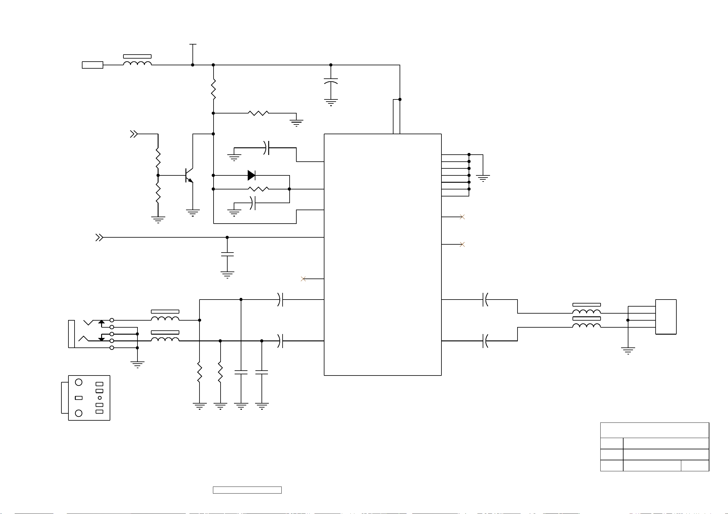
+12V
AUDIO_STANBYP3
MUTE ACTIVE LOW
L608
3.5X9*0.8
R611
10K
DC12_AUDIO
R610
10K
Q601
2SC945
R606 used jump line,first.
+
R620
4.7K
R602 3.9K
C610
220u/16V
D601 1N4148
R601 100K
+
C602
22u/16V
+
10
12 19
11
C601
1000u/16V
I601
TDA7496L
SVR
MUTE GND6
STBY
161415
VP2
VP1
VAROUT_L
GND1
GND2
GND3
GND4
GND5
GND7
1
2
3
13
18
20
5
VOLUMEP3
P603
VOLUME
AUDIO INPUT (GREEN)
L
5
LS
4
RS
3
R
2
S
1
5
1
4
3
2
L601
3.5X6X2
L602
3.5X6X2
R61222K
C615
0.1u
R61322K
6
VOLUME
VAROUT_R
8
C604
1u/50V
+
C603
1u/50V
+
C616NC
C617
NC
NC
4
INL
9
INR
OUTL
OUTR
7
C605 470u/16V
17
+
C606 470u/16V
+
L_OUT
R_OUT
L603
3.5X9*0.8
L604
3.5X9*0.8
P601
4
L-
3
L+
2
R-
1
R+
SOCKET
TO SPEAER
SOLDER
SIDE
ViewSonic Corporation Confidential - Do Not Copy
61
Q9b-3
ViewSonic Corporation
Model
Title
Date Rev:
AUDIO

12V
Q907 2SC945P
ON/OFF
L901
Bead core 9mm
Brightness
C910
0.01uF
D916
1N4148
5V
D921
NC
D920
NC
3 1
2
D9151N4148
C901
47nF
R90810K
R903
NC
I902NC
IN OUT
GND
R922 5.62M 1%
5V
R92910K
R918 107K 1%
D9191N4148
C928
0.1uF
D901
JUMPER WIRE
+
C915
NC
OZ9936G
1
SST
2
RT
3
GNDA
4 5
DRV2 DRV1
J906
22R
I901
ISEN
VSEN
VCCA
Q901
2SC945P
C925
0.1uF
T901
71,2
C902
22P,3KV
105,6
C905
5P,3KV
C908
4700PF/50V
71,2
105,6
C916
22P,3KV
C919
4700PF/50V
C909
NC
C918
5P,3KV
C920
NC
D907
1N4148
1N4148
D913
1N4148
D908
1N4148
C912
0.01uF
3.3K/1%
D910
R909
0.01uF
C913
R905
3M,3KV
R925
3M,3KV
R927
3.3K/1%
R910
NC
R928
NC
R920
2K
D912
1N4148
D918
1N4148
D902
1N4148
D917
1N4148
C906 470uF/16V
3,4
2374301405P
D905
1N4148
D906
1N4148
T902
3,4
2374301405P
D911
1N4148
D909
1N4148
C9042200P
R9074.7
6
7
8
1
2
3
4 5
R923
NC
8
7
6
C917
1000pF
J907
22R
NC
R926
R9064.7
Q905
AP9977GM
R924
1M
Q908
2SC945P
C927
2200P
7
8
1
2
C914
0.1UF
R9124.7
6
3
C9032200P
R913
10K
Q909
2N7000P/TO_0
Q911
AP9977GM
4 5
R9143.3K
R9114.7
C926
2200P
C921
0.01uF
+
C907 0.01uF
+
C922 470U/16V
P901
1
2
P902
1
2
C911
0.1UF
P903
1
2
P904
1
2
ViewSonic Corporation Confidential - Do Not Copy
62
Q9b-3
C924
68nF
R937
392R/1%
R936
NC
ViewSonic Corporation
Model
Title
Date Rev:
Inverter

R820
22 1W
C820
2200PF/500V
2KBP06M
- +
R801 NA
R802
10 3A
R812
910K/1/4WS
R803
910K/1/4WS
C801
0.47uF
D801
L805
ET-20
T801 ER28H 12PIN 2374228031P
R833
+
R839 619K 1%
C805 100uF/400V
R844 619K 1%
R805 619K 1%
8
HV
I801 LD7575
Adj
1
R808
107K/1%
100K/1/4WS
R806 10K
100K/1/4WS
R843
Jumper
R804 Jumper
6
7
NC
FB
2
3
R834
FERRITE CORE 6*10/3Ts
L806
+
C810
10UF/50V
5
Drv
Vcc
GND
CS
4
C807
NC
C808 470P
R835
100K/1/4WS
R836
100K/1/4WS
C809
820R/1/4WS
+
NC
R807 39
R832
C806
1000PF/1KV
220pF/1KV
C828
D806
UF4007
D807 UF4004G
R810
NC
L801
3.5*0.8*4.5
Q801
AP04N70BF-A/H
R809
10K
R852 NC
3
57
1
4
12
5
C831
0.01uF
C813
NC
R823
100
R811 0.56R/ 2WS
11,12
5
R821
9
22 1/2W
D823 31DQ06
10
4
D822 31DQ06
7,8
D821
GMR10H125C
C821
2200PF/500V
R831
100
C822
1000uF/16V
L804
5.2UH
+
C824
1000UF/10V
3.6K 1%
R827
1K
+
R824
L803
5.2UH
+
C829
1000uF/16V
R850 NC
+
C825
Z802
HZ12A-3
12V
+
C823
R837
220R/2WS
F802
JUMPER
470uF/16V
HZ12A-3
Q802
2SC945P
470uF/16V
5V
R854
100
Z801
R828
33K 1%
4
L802
3.5*9*0.8
C803
4700pF
S801
F801
T2.5A/250V
L
FG
L808
jumper wire
C802
4700pF
N
3
TLP621
AC IN 100~240V
ViewSonic Corporation Confidential - Do Not Copy
63
I802
1
2
10UF/50V
Q9b-3
C827
R825
1.21K 1%
R842
1K
I803
+
TL431D
C826
0.1U
R851
1.21K 1%
ViewSonic Corporation
Model
Title
Date Rev:
JT198NP4FD3

11. PCB Layout Diagrams
POWER PCB TOP VIEW
ViewSonic Corporation Confidential - Do Not Copy
64
Q9b-3

POWER PCB BOTTOM VIEW
ViewSonic Corporation Confidential - Do Not Copy
65
Q9b-3

CON PCB TOP VIEW
CON PCB BOTTOM VIEW
ViewSonic Corporation Confidential - Do Not Copy
66
Q9b-3

* Reader’s Response*
Dear Readers:
Thank you in advance for your feedback on our Service Manual, which allows continuous improvement
of our products. We would appreciate your completion of the Assessment Matrix below, for return to
ViewSonic Corporation.
Assessment
A. What do you think about the content of this Service Manual?
Unit Excellent Good Fair Bad
1. Precautions and Safety Notices
2. Specification
3. Front Panel Function Control Description
4. Circuit Description
5. Adjustment Procedure
6. Troubleshooting Flow Chart
7. Recommended Spare Parts List
8. Exploded Diagram and Exploded Parts List
9. Block Diagrams
10. Schematic Diagrams
11.PCB Layout Diagrams
B. Are you satisfied with this Service Manual?
Item Excellent Good Fair Bad
1. Service Manual Content
2. Service Manual Layout
3. The form and listing
C. Do you have any other opinions or suggestions regarding this service manual?
Name:
Reader’s basic dada:
Title:
Company:
Add:
Tel:
Fax:
E-mail:
After completing this form, please return it to ViewSonic Quality Assurance in the USA at facsimile
1-909-839-7943. You may also e-mail any suggestions to the Director, Quality Systems & Processes
(marc.maupin@viewsonic.com)
ViewSonic Corporation Confidential - Do Not Copy Q9b-3
67
 Loading...