


1
SERVICE MANUAL
COLOR MONITOR
(Q51/E50C Series)
THESE DOCUMENTS ARE FOR REPAIR SERVICE INFORMATION ONLY. EVERY REASONABLE EFFORT
HAS BEEN MADE TO ENSURE THE ACCURACY OF THIS MANUAL; WE CANNOT GUARANTEE THE
ACCURACY OF THIS INFORMATION AFTER THE DATE OF PUBLICATION AND DISCLAIMS LIABILITY FOR
CHANGES, ERRORS OR OMISSIONS,
MANUFACTURE DATE: DEC.2004

2
TABLE OF CONTENTS
CONTENTS PAGE
1. SPECIFICATIONS ....................................................................................................…......... 3
2. PRECAUTION AND NOTICES ............................................…............................................. 4
2-1 SAFETY PRECAUTIONS ......................................................................…................... 4
2-2 PRODUCT SAFETY NOTICE .....................................................…….......................... 5
2-3 SERVICE NOTES ................................................................................……................. 6
2-4 HIGH VOLTAGE WARNING ........................................................…………….............. 6
3. OPERATING INSTRUCTIONS ..............................................................……………............ 7
4. ADJUSTMENT ......................................................................................…………….............. 8
4-1 ADJUSTMENT CONDITIONS AND PRECAUTIONS ...............………………….......... 8
4-2 MAIN ADJUSTMENTS ...........................................................…………….................... 8
4-3 ADJUSTMENT METHOD .....................................................……………...................... 8
4-4 EDID CONTENTS ....................................................……………….............................. 13
5. CIRCUIT DESCRIPTION ..............................................…………......................................... 13
6. TROUBLE SHOOTING CHART .....................................……………..................................... 16
6.1 NO RASTER, CRT RELATIVE CIRCUIT PROBLEMS ..........………………............. 16
6.2 ABNORMAL DISPLAY .................................................................……………………… 18
6.3 NO BLANKING ....................................……………………………………………………. 19
6.4 HOR./OSC/DEF/HV CIRCUIT FAULT ........................…………………………............. 19
6.5 ABNORMAL HORIZONTAL DEFLECTION ................…………………………………... 20
6.6 ABNORMAL VERTICAL SCANNING ...................................……………….................. 21
6.7 SIDE-PINCUSHION Distortions ....................................…………………………………. 21
6.8 POOR FOCUS ........................................................................………………………….. 21
6.9 POWER SUPPLY TROUBLE SHOOTING CHART.............................…………………. 22
7. MECHANICAL OF CABINET FRONT DIS-ASSEMBLY……………..................................... 23
8. BOM LIST .................................................................…………………................................ 26
9. BLOCK DIAGRAM............………………………………………………………………………… 41
9.1 BLOCK DIAGRAM (SMPS) ............…………………………………………………………
41
9.2 IC BLOCK DIAGRAMS ……………………………………………………………………… 42
10. PCB LAYOUT ................................................................……………….................................. 49
11. SCHAMATIC ……………………………………………………………………………………….. 51
3
1. SPECIFICATIONS FOR Q51/E50C SERIES COLOR MONITOR
CRT:
Type 15" (13.8” viewable diagonal area) CPT M36AES83X01 (L), LPD M36EDR320X304/6F01L;Dot Pitch 0.28 mm,
Shadow Mask, None Glare.
Viewable image Size: 35CM (13.8”) diagonal
Display Color: Unlimited Colors
External Controls:
Power On/Off, OSD key, Function knob: Contrast, Brightness, and Degauss. Horizontal Size, Horizontal Position,
Vertical Size, Vertical Position, Pincushion, Pincushion Balance, Trapezoid, Parallelogram, Tilt, Horizontal Moire,
Vertical Moire, ViewMatch color, ViewMeter, OSD Position, Languages, Memory Recall, Zoom.
Input Video Signal:
Timing Timing 15 Timing 16 Timing 17
Resolution
720*400 640*480 640*480
H (KHz)
31.327 31.469 37.5
V (Hz)
69.616 59.943 75.00
Timing Timing27 Timing 29
Timing37
Resolution
800*600 800*600 1024*768
H (KHz)
46.875 53.674 48.36
V (Hz)
75.00 85.061 60.00
Display Size:
Horizontal Display Size, Primary Preset 270 mm +/- 4 mm
Horizontal Display Size, Other Presets 270 mm +/- 4 mm
Vertical Display Size, Primary Preset 202 mm +/- 4 mm
Vertical Display Size, Other Presets 202 mm +/- 4 mm
Display Size Adjustment
All preset modes shall expand to
full screen size.
Scanning Frequencies:
Horizontal: 30KHz ~ 54KHz
Vertical: 50 Hz ~ 120 Hz
Factory Preset Timings: 6
User Timings: 19
4
Mis-convergence:
A Zone 0.25 mm
B Zone 0.30 mm
C Zone 0.35mm
Power Source:
Switching Mode Power Supply
AC 90-264 VAC 50/60 Hz
ENVIRONMENTAL
Operating Temperature 0°C to +40°C
Storage Temperature -40°C to +60°C
Operating Relative Humidity 5% to 95% Non-Condensing
Storage Relative Humidity 5% to 95% Non-Condensing
Operating Altitude -400 meters to +3000 meters
Storage Altitude -400 meters to +12,000 meters
Gross Weight: 13.0 kg
Dimensions Monitor:
Carton: 438mm (W) x 385 mm (H) x 455 mm (D)
Monitor: 360 mm (W) x 362 mm (H) x 384 mm (D)
External Connection:
15 Pin D-type Connector AC Power Cord
Regulations:
North America (M): UL/cUL, DHHS, TUV/S (Argentina) FCC-B, NOM, ICES-003, BSMI, PSB
International: CB, MPRII.
Power Saving Operation:
ON Mode < 70 Watts
OFF < 5 Watts

5
2. PRECAUTIONS AND NOTICES
2-1 SAFETY PRECAUTIONS
1. Observe all caution and safety related notes located inside the display cabinet.
2. Operation of the display with the cover removed, may cause a serious shock hazard from the display power supply.
Work on the display should not be attempted by anyone who is not thoroughly familiar with precautions necessary
when working on high voltage equipment.
3. Do not install, remove or handle the picture tube in any manner unless shatter-proof goggles are worn. People who
are not so equipped should be kept away while handling picture tube. Keep picture tube away from the body while
handling.
4. The picture tube is constructed to limit X-RAY radiation to 0.5 mR/HR. For continued protection, use the
designated replacement tube only, and adjust the voltages so that the designated maximum rating at the anode will
not be exceeded.
5. Symbol “
!
” means safety relative parts. The use of substitute replacement parts which do not have the same
characteristics as specified in the parts list may create shock, fire or explode etc.
6. Symbol “★ ” means X-ray relative parts. Before replacing any of these components please read the parts list in this
manual carefully to avoid creating higher anode voltage or x-ray. Especially for sealed controls, such as VR901
VR902, VR701 and FBT screen VR etc, which were sealed by the manufacturer once their optimum position has
been set, please don’t dismantle them as your likes, otherwise you will break or damage the component. If you
need replace the parts with sealed control, please adjust the relative VR to make sure the B+ voltage under
59.0+
0.2Vdc at 640x480 60Hz and well seal it with A+B glue or equivalent, which you can not move away with
one screw driver.
7. Before returning a serviced display to the customer, a thorough safety test must be performed to verify that the
display is safe to operate without danger or shock. Always perform an AC leakage current check on the exposed
metallic parts of the cabinet, such as screw heads.
Test method for current leakage is described as follow.
(a) Plug the AC line cord directly into rated AC outlet (do not use a line isolation transformer during this check).
(b) Use an AC voltmeter having 5000 ohms per volt or with more sensitivity in the following manner: Connect a
1500 ohms 10 Watt resistor, paralleled by a 0.15UF, AC type capacitor between a known good earth ground
(water pipe, conduit, etc.) and the exposed metallic parts simultaneously. Measure the AC voltage across the
combination of 1500 ohms resistor and 0.15UF capacitor.
(c) Reverse the AC plug at the AC outlet and repeat AC voltage measurements for each exposed metallic part.
(d) Voltage measured must not exceed 0.5 volts RMS. This corresponds to 0.35 milliamp AC. Any value
exceeding this limit constitutes a potential shock hazard and must be corrected immediately.
2.2 PRODUCT SAFETY NOTICE
Many electrical and mechanical parts in this chassis have special safety visual inspections and the protection afforded
by them cannot necessarily be obtained by using replacement components rated for higher voltage, wattage, etc. Before
replacing any of these components read the parts list in this manual carefully. The use of substitute replacement parts
which do not have the same safety characteristics as specified in the parts list may create shock, fire, X-RAY radiation
or other hazards.

6
2.3 SERVICE NOTES
1. When replacing parts or circuit boards, clamp the lead wires around terminals before soldering.
2. When replacing a high wattage resistor (more than 1/2W of metal oxide film resistor) in circuit board, keep the
resistor about 10mm (1/2 in) away from circuit board.
3. Keep wires away from high voltage or high temperature components.
4. Keep wires in their original position so as to reduce interference.
2.4 HIGH VOLTAGE WARNING
Operation of monitor outside of cabinet or with back removed may cause a serious shock hazard. Work on this model
should only be performed by those who are thoroughly familiar with precautions necessary when working on high
voltage equipment.
Exercise care when servicing this chassis with power applied. Many B plus and high voltage terminals are exposed
which, if carelessly contacted, can cause serious shock or result in damage to the chassis. Maintain interconnecting
ground lead connections between chassis and picture tube dag when operating chassis.
Certain HV failures can increase X-ray radiation. Monitor should not be operated with HV levels exceeding the
specified rating for the chassis type. The maximum operating HV specified for the chassis used in this monitor is
25.5KV ± 1KV
With a line voltage of 120/240 VAC. Higher voltage may also increase possibility of failure in HV supply.
It is important to maintain specified values of all components in the horizontal and high voltage circuits and anywhere
else in the monitor that could cause a rise in high voltage or operating supply voltages. No changes should be made to
the original design of the monitor. Components shown in the shaded areas on the schematic should be replaced with
exact factory replacement parts. The use of unauthorized substitute parts may create a shock, fire or other hazard.
To determine the presence of high voltage, use accurate, high impedance, HV meter connected between second anode
lead and CRT dag grounding device. When servicing the High Voltage System, remove static charge from it by
connecting a 20K ohm resistor in series with an insulated wire (such as a test probe) between picture tube dag and 2nd
anode lead. (AC line cord disconnected from AC power outlet.)
The picture tube used in this monitor employs integral implosion protection. Replace with tube of the same type number
for continue safety. Do not lift picture tube by the neck. Handle the picture tube only after discharging the high voltage
completely.
7
3. OPERATING INSTRUCTIONS
This procedure gives you instructions for installing and using the Q51/E50C color display.
1. Position the display on the desired operation and plug the power cord into a convenient AC outlet. Three-wire
power cord must be shielded and is provided as a safety precaution as it connects the chassis and cabinet to the
electrical conduit ground. If the AC outlet in your location does not have provisions for the grounded type plug,
the installer should attach the proper adapter to ensure a safe ground potential.
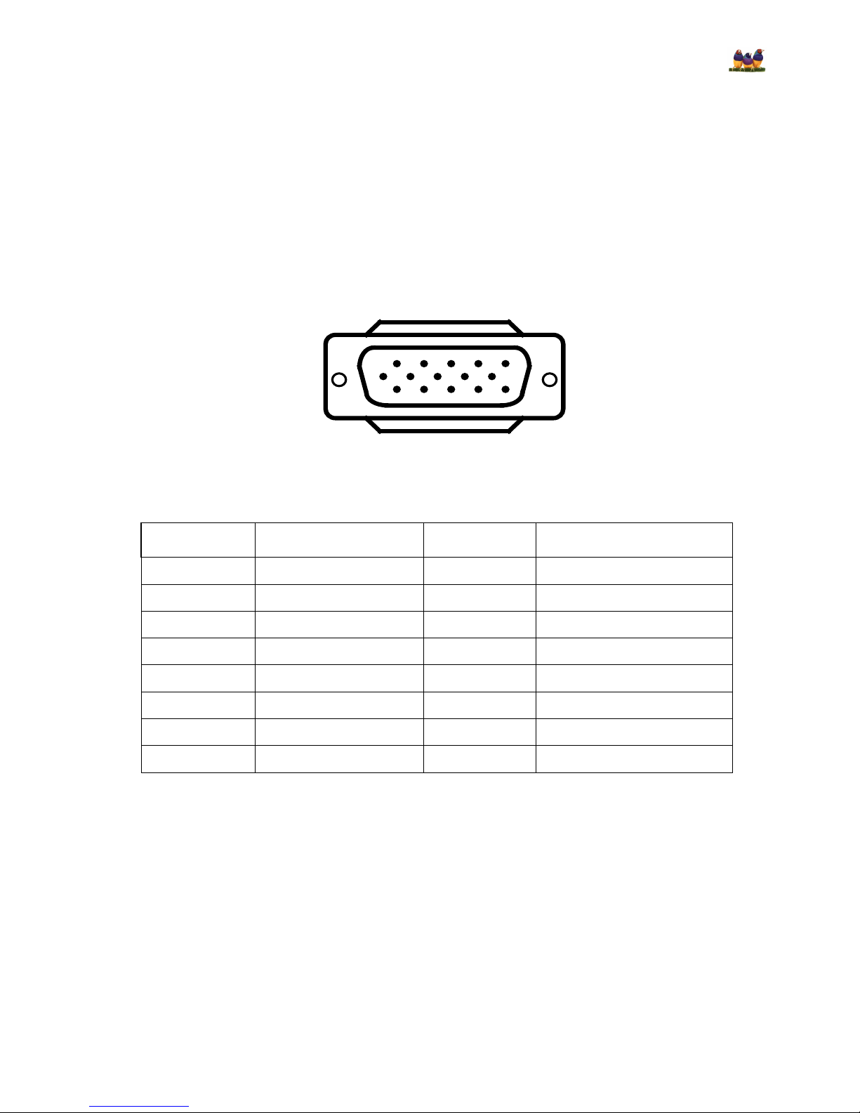
2. Connect the 15-pin color display shielded signal cable to your signal system device and lock both screws on the
connector to ensure firm grounding. The connector information is as follow:
15 - Pin Color Display Signal Cable
3. Apply power to the display by turning the power switch to the "ON" position and allow about thirty seconds for
display tube warm-up. The Power-On indicator lights when the display is on.
4. With proper signals feed to the display, a pattern or data should appear on the screen, adjust the brightness and
contrast to the most pleasing display.
5. This monitor has power saving function following the VESA DPMS. Be sure to connect the signal cable to the PC.
6. If your Q51/E50C Series color display requires service, it must be returned with the power cord.
1
6
11 15
5
10
PIN NO. DESCRIPTION PIN NO. DESCRIPTION
1. RED 9. NC
2. GREEN 10. GND
3. BLUE 11. SYNC. GND
4. GND 12. SDA
5. GND 13. HORIZ. SYNC
6. GND-R 14. VERT. SYNC
7. GND-G 15. SCL
8. GND-B
8
4. ADJUSTMENT
4. 1 ADJUSTMENT CONDITIONS AND PRECAUTIONS
1. Approximately 30 minutes should be allowed for warm up before proceeding.
2. Adjustments should be undertaken only on those necessary elements since most of them have been carefully preset
at the factory.
4. 2 MAIN ADJUSTMENTS
NO. FUNCTION LOCATION DESIGNATION
1. 14.5V ADJ PCB - MAIN VR901
2. B + ADJ PCB - MAIN VR902
3. SCREEN ADJ FLY BACK TRANS T402
4. FOCUS ADJ FLY BACK TRANS T402
-MENU PCB - MAIN SW102
-UP
PCB - MAIN SW103
5. FUNCTION ADJ -DOWN PCB - MAIN SW104
-EXIT PCB - MAIN SW105
4. 3 ADJUSTMENT METHOD
14.5V, B + & HV voltage adjustment:
A. Chroma-2000 Signal generator or PC equivalent set mode2:, VGA 640X480 pattern 1.0.
B. Connect a DC Volt meter between TP901 (or the equivalent point) and ground, then adjust VR901 to be 14.2VDC.
C. Connect a DC Volt meter between TP902 (or the equivalent point) and ground, then adjust VR902 to be 85 VDC.
Factory preset Timings Adjustment:
A. Press Encoder control Key to show OSD window then press again to switch the functional controls.
B. Select to the "ZOOM" function, then press the button while does not release until the OSD window changed to the
Factory preset window.
C. The Factory preset window contains the following functional controls. Select one of the controls to adjust its value
for the optimum picture.
White Balance adjustment(Bias ,Gain, ABL):
A. Bias (Raster luminance and cut off ) adjustment:
(a) Set mode 5 800×600 Fh: 53KHz full white pattern.
(b) To make the adjustment condition is under the Factory preset window.
Same as step 2-C.
(c) Warm up more than 20 minutes.
(d) Change pattern to mode 5 Raster pattern (only Raster, no video), Brightness
set to maximum. Contrast
set to min., G-Bias 40, then adjust FBT screen VR. R-Bias . B-Bias to make Y= 3.5
±0.2cd/m², x= 265 ± 5, y= 290 ± 5.
(e) Raster cut off adjustment: adjustment the Brightness makes the Y=0.08±0.02cd/m², then save the adjustment
data to 9300 and 6500.

9
B. Gain (window white luminance) adjustment:
(a) Set mode 5 800×600 Fh: 53KHz window white pattern (100mm*100mm window).
(b) Brightness set to raster just cutoff and set the contrast to max.
(c) Adjust G-Gain
, B-Gain , R-Gain , to make color temperaturem Y=140±2 cd/m². x=283 ±
5, y=297 ± 5. then save to 9300
(d) Adjust G-Gain
, B-Gain , R-Gain , to make color temperaturem Y=140±2 cd/m². x=313 ±
5, y=329 ± 5. then save to 6500.
C. Recheck item A&B to make sure both of them in spec. Finally select OSD function to the 9300°K function, then
press to make the setting data saved in the memory.
D.ABL(Full white luminance) adjustment:
(a) Set mode 5 800×600 Fh: 53KHz full white pattern.
(b) Image Size: H: 270±3mm V: 202±3mm.
(c) Brightness set to raster just cut off and set the contrast to max.
(d) Adjust AB icon to the luminance at 103 ±1cd/m².
Focus Adjustment:
A. Set mode 5 800×600 Fh: 53KHz with character full page.
B. Adjust brightness to center and contrast to max.
C. Then adjust focus VR to a fine vertical and horizontal line.
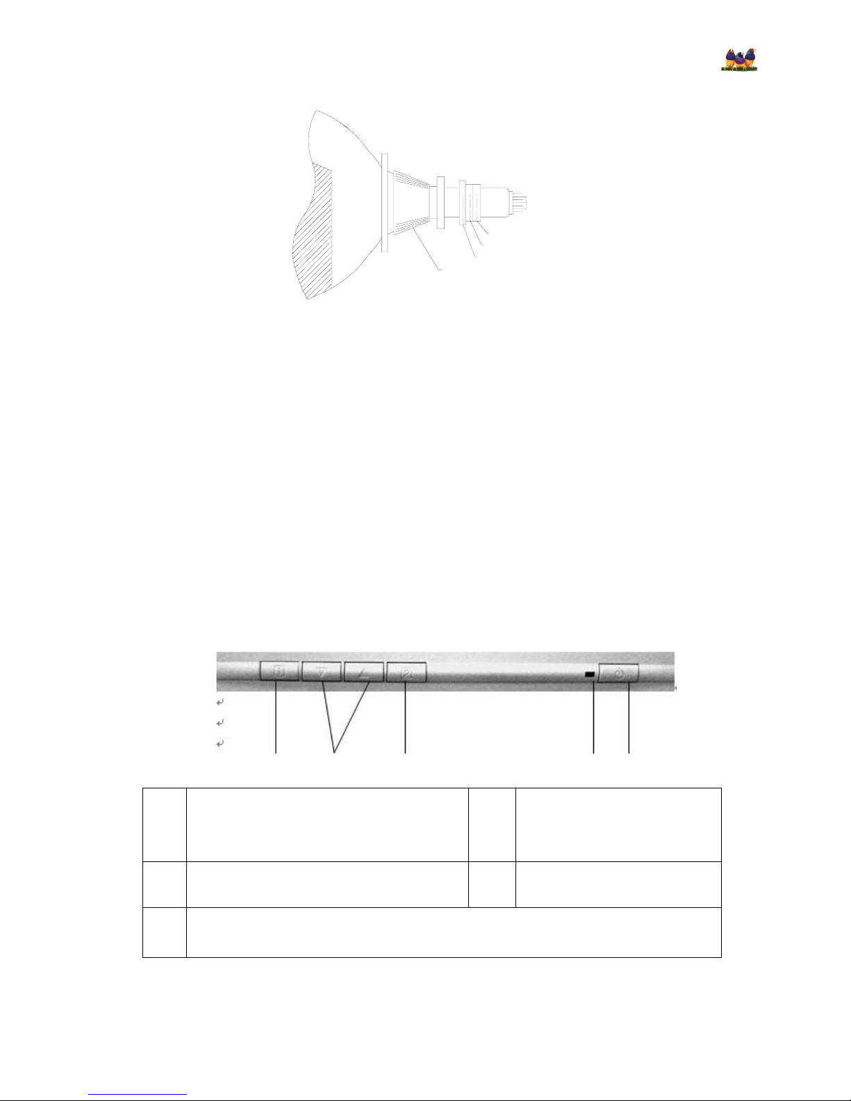
Purity Adjustment
A. Be sure that the display is not being exposed to any external magnetic fields.
B. Ensure that the spacing between the Purity, Convergence, Magnet, (PCM), assembly and the CRT stem is 29mm.
(See below diagram)
C. Produce a complete, red pattern on the display. Adjust the purity magnet rings on the PCM assembly to obtain a
complete field of the color red. This is done by moving the two tabs in such a manner that they advance in an
opposite direction but at the same time to obtain the same angle between the two tabs, which should be
approximately 180'.
D. Check the complete blue and complete green patterns to observe their respective color purity. Make minor
adjustments if needed.
10
RELATIVE PLACEMENT OF TYPICAL COMPONENTS
Purity Magnets
Deflection Yoke
4-pole Convergence Magnets
6-pole Convergence Magnets
Convergence adjustment
A. Produce a magenta crosshatch on the display.
B. Adjust the focus for the best overall focus on the display.
Also adjust the brightness to the desired condition.
C. Vertical red and blue lines are converged by varying the angle between the two tabs of the 4 pole magnets on the
PCM assembly. (See above diagrams)
D. Horizontal red and blue lines are converged by varying the two tabs together, keeping the angle between them
constant.
E. Produce a white crosshatch pattern on the display.
F. Vertical green and magenta lines are converged by varying the angle between the two tabs of the 6-pole magnets.
G. Horizontal green and magenta lines are converged by varying the two tabs together, keeping the angle between
them constant.
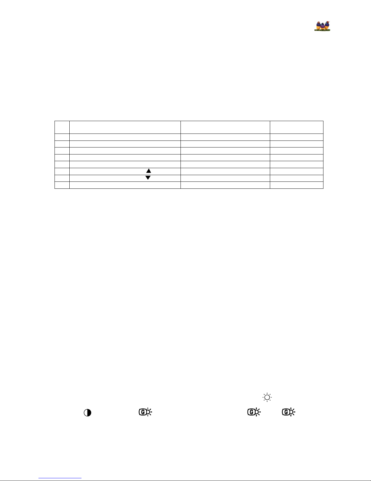
OSD OPRATION
1
Displays Main Menu; also saves
Changes/exits Main Menu
4
Power Light
2
Scroll through menu
options and adjust the
displayed control
5
Power On/Off
3
Displays control screen for highlighted control (or pair of controls). Also, toggles between pairs of
controls on some control screens
1 2 3 4 5
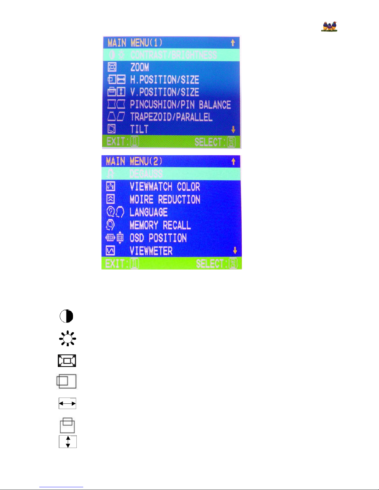
11
Contrast adjusts the difference between the image background (black level) and the foreground (white
level)
Brightness adjusts the background black level of the screen image.
Zoom expands and contracts the entire screen image.
Horizontal Position moves the screen image left or right.
Horizontal Size adjusts width of the screen image.
Vertical Position moves the screen image up or down.
Vertical Size adjusts the height of the screen image.
User MENU 1
User MENU 2

12
Pincushion curves the vertical sides of the screen image.
Pin Balance curves the vertical edges of the screen image to the left or right.
Trapezoid adjusts the top and bottom of the screen image until they have equal length.
Parallel slants the vertical edges of the screen image until they are parallel.
Tilt rotates the entire screen image.
Degauss removes the build-up of magnetic fields that can cause irregular colors to appear around the edges of
screen images. There are two ways to degauss the display: automatically by turning the monitor on, or
manually by selecting the Degauss control from the menu.
With Degauss selected from the menu, press button [2] to degauss the monitor manually. Important: Do not
degauss repeatedly. Doing so can be harmful to the display. Wait at least 20 minutes (before selecting this
control again.
ViewMatch® Color provides several color options: several preset color temperatures and User Color which
allows you to adjust red (R), green (G), and blue (B). The factory setting for this product is 9300K (9300°
Kelvin).
9300K — Adds blue to the screen image for cooler white (used in most office settings with fluorescent
lighting).
6500K — Adds red to the screen image for warmer white and richer red.
5000K — Adds blue and green to the screen image for a darker color.
User Color — Individual adjustments for red, green, and blue.
Moire reduces interference patterns that appear as ripples, waves, or unwanted background color textures.
Interference patterns of this type are most noticeable when viewing images having closely spaced lines or
finely detailed patterns.
Language allows you to choose from among several languages for the menus and control screens: English,
French, German, Italian, and Spanish.
Memory Recall returns adjustments to the original factory settings if the display is operating in a factory preset
timing mode listed in this user guide.
Exception: This control does not affect changes made with the User Color control.
OSD Position allows you to move the on-screen display menus and control screens.
ViewMeter displays the frequencies (horizontal and vertical) coming from the graphics card of the computer.

13
4.4 EDID CONTENTS
0 1 2 3 4 5 6 7 8 9
________________________________________
0 | 00 FF FF FF FF FF FF 00 5A 63
10 | 1B 85 01 01 01 01 01 0E 01 03
20 | 1D 1C 15 B0 2A E0 58 9F 54 46
30 | 9B 24 10 48 4C FF F8 00 45 59
40 | 31 59 01 01 01 01 01 01 01 01
50 | 01 01 01 01 F9 15 20 F8 30 58
60 | 1F 20 20 40 13 00 0E CA 10 00
70 | 00 1E 00 00 00 FF 00 50 4C 36
80 | 30 34 30 31 30 30 30 30 31 0A
90 | 00 00 00 FD 00 32 78 1E 36 08
100 | 00 0A 20 20 20 20 20 20 00 00
110 | 00 FC 00 51 35 31 2D 39 0A 20
120 | 20 20 20 20 20 20 00 A4
5. CIRCUIT DESCRIPTION
5.1 MICRO CONTROLLER CIRCUIT
MICRO Controller
The IC101 contains a 8031 8-bit CPU core, 512 bytes of RAM, 32K bytes of ROM, 10 channel 8 bit PWM D/A
converters, 4 channel A/D converters, 216 bit timer/counters, internal H-sync and V-sync signals processor providing
mode detection, watch- dog timer preventing system from abnormal operation, and an I
2
C bus interface.
H/V sync signals processor
The functions of the sync processor include polarity detection, H-SYNC & V-SYNC signals counting, and
Programmable SYNC signals output, free running signal generator. Pin41/Pin42 are for the H-SYNC and V-SYNC input,
Pin34/Pin33 will output the same signal as input sync signal without delay, and the polarity is setting in the positive.
When no signal input, the Pin34 and Pin33 will output a free run signal for the monitor testing use.
On Screen Display Controller
The IC801 is designed for pre-amp and displaying the built-in characters or fonts onto monitor screen. The display
operation is by transforming data and control information from micro controller to RAM through a serial data interface.
Pin14/15/16 are used to output the B/G/R-bias.
Pin21/20/19 are used to output the B/G/R-gain.
Pin5/6/7 are used to input the R/G/B signal.
Pin11/12 are SDA/SCL.
Pin22 is used for the automatic Beam Limiter input.
Pin1, V Fly back, required for OSD synchronization and is also used for vertical blanking of the video outputs.

14
Pin2, V ref Bypass, provides filtering for the internal voltage.
Pin3, Vref, sets the internal bias current level for optimum performance.
5.2 DEFLECTION CIRCUIT
The deflection circuit is achieved by a high performance and efficient solution IC 401 (TDA4841) for this monitor. All
functions are controllable by IIC –bus.
The TDA4841 provides sync. Processing with full auto sync. Capability, a flexible SMPS block and an extensive set of
geometry control facilities. Further the IC generates the drive waveforms for DC coupled vertical boosters such as
TDA486*/TDA835*.
Horizontal Oscillator
The oscillator is of the relaxation type and requires a capacitor at pin29. A resistor from pin28 to ground determines the
minimum oscillator frequency. A resistor from pin28 to pin27 defines the frequency range.
PLL 1 Phase Detector
The phase detector is a standard one using switched current sources. It compares the middle of H-sync with a fixed
point on the oscillator saw-tooth voltage. The PLL loop filter is connected to Pin26.
PLL2 Phase Detector
This phase detector is similar to the PLL1 detector and compares the line fly back pulse with the oscillator saw-tooth
voltage. The PLL2 detector thus compensates for the delay in the external H-deflection circuit by adjusting the phase of the
HDRV output pulses. The phase between H-fly back and H-sync can be controlled at pin30.
X-ray Protection
The X-ray protection input pin2 provides a voltage detector with a precise threshold. If the voltage exceeds this
threshold for a certain time, an internal latch switches the whole IC into protection mode. In this mode several pins are
forced into defined states:
Pin6 (BDRV) is floating
Pin8 (HDRV) is floating
Pin13/12 (VOUT1 and VOUT2) are floating
Vertical Oscillator
The vertical free –running the capacitor at pin24 and the resistor at pin23 determine frequency. Usually the free-running
frequency should be lower than the minimum trigger frequency.

15
5.3 TRANSISTOR & DIODE CIRCUIT
LOCATION
CIRCUIT FUNCTION DESCRIPTION
D901 ~ D904 BRIDGE RECTIFIER FOR AC SOURCE
D918, D919 RECTIFIER FOR OUTPUT VOLTAGE
D921 RECTIFIER FOR OUTPUT VOLTAGE
D922 RECTIFIER FOR OUTPUT VOLTAGE
D923 RECTIFIER FOR OUTPUT VOLTAGE
D925 RECTIFIER FOR B+ OUTPUT VOLTAGE
D929 B+ FEED BACK RECTIFIER FROM F.B.T PULSE
Q907, Q908 USE FOR OFF-MODE TO CUT-OFF 6.3V SUPPLY VOLTAGE
Q909, Q910 USE FOR OF- MODE TO CUT-OFF 14.2V SUPPLY VOLTAGE
Q912, Q920 PUSH-PULL TOPOLOGY TO DRIVE Q911
Q913 DEGAUSSING SWITCHER TRANSISTOR
Q921 5V REGULATOR TRANSISTOR
Q401 TURN-ON AT POWER ON/OFF AND CHANGE MODE TO PROTECT HOR.BLOCK
Q460 HOR. DRIVER TRANSISTOR
Q408 AS A SWITCHER FOR HORIZONTAL S CORRECTION CKT
Q410 HORIZONTAL S CORRECTION CONTROL MOSFET
Q404, Q405 AS DIFFERENTIAL AMP. TO DRIVE Q406
Q406 DARLINGTON TRANSISTOR FOR H-SIZE CONTROL
Q705 G1 CONTROL CKT
16
6. TROUBLE SHOOTING CHART
6.1 NO RASTER, CRT RELATIVE CIRCUIT PROBLEMS
N
G
CHECK THE HIGE VOLTAGE
OF CRT ABOUT 24.5~25.5V
CHECK LOWER POWER CIRCUIT
H-SYNC,V-SYNC SIGNAL
Q909,Q910
CHECK MAIN PCB POWER
SUPPLY 76V,14.2V
CHECK THE VOLTAGE OF CRT
HEATER ABOUT 6.3V
CHECK FAILSAFE CKT IC401 PIN2
RELATIVE CKT.
REFER ITEM S.M.P.S
O
K
N
G
OK
CHECK CRT’S HEATER RELATIVE
CIRCUIT D923
CHECK SCREEN VOLTAGE
ABOUT 500V TO 700V
BRIGHTNESS SET TO MAX
CHECK VOLTAGE OF THE CRT
CATHODE ABOUT 40Vpp
CHECK FBT
LESS THAN 300V
CHECK G1 CIRCUIT Q705
RELATIVE CKT
REFER ITEM 6-2 “ABNORMAL
DISPLAY”
NG NG N
G
OK
OK
OK
OK
17
2.ABNORMAL VIDEO LEVEL ON SCREEN
3.ABNORMAL DDC (PLUG & PLAY)
NG
OK
CHECK IC101 PIN5 VOLTAGE
ABOUT:5V
CHECK SIGNAL CABLE OR H802
PIN4/5
CHECK Q921 GOOD OR FAIL
CHECK THE VOLTAGE OF IC801
PIN10/18 ABOUT 5V
CHECK 5V RELATIVE
CIRCUIT
CHECK THE IC801 PIN23
RELATIVE CIRCUIT
CHECK IC801 PIN5/PIN6/PIN7
RELATIVE CIRCUIT
CHECK THE VIDEO OUTPUT OF
IC801 PIN19/20/21 ABOUT 3Vpp
AND PIN14/15/16 ABOUT 2V
CHECK IC801 PIN23 CLAMP
PULSE
CHECK THE SIGNAL INPUT OF
R.G.B
ABOUT 0.7V
pp
CHECK SIGNAL CABLE OR
INTERFACE CARD.
R.G.B APPROACH STANDARD
OK
N
G
OK
N
G
OK
N
G
O
K

18
6.2 ABNORMAL DISPLAY
NO SIGNAL ON SCREEN
EXCEED 700V
CHECK VIDEO IC801 VCC ABOUT
5V
CHECK THE 5V PIN OF P802
CONNECTOR
CHECK THE RELATIVE CIRCUIT
OF IC801 PIN23 CIRCUIT
NG
CHECK THE OUTPUT VOLTAGE
OF IC801 PIN19/20/21 ABOUT 3Vpp
CHECK THE VIDEO 80V OF IC802
PIN4 ABOUT 77V
CHECK THE 80V RELATIVE
CIRCUIT OF SMPS ON MAIN PCB
NG NG
CHECK THE VOLTAGE OF CRT
CATHODE ABOUT 40Vpp
NG
CHECK THE IC802 RELATIVE
CIRCUIT
CHECK THE IC803 PIN6, 7,8 VOLTAGE
ABOUT 50VDC RELATIVE CIRCUIT
CHECK THE VOLTAGE OF FBT
SCREEN ABOUT 400V TO 700V
NG
CHECK THE IC803 RELATIVE
CIRCUIT
CHECK FBT RELATIVE CIRCUIT
LESS THAN 400V
CHECK FBT&CRT RELATIVE
CIRCUIT OR REFER ITEM6-1

19
6.3 NO BLANKING
NG
OK
6.4 HOR./OSC/DEF/HV CIRCUIT FAULT
NO RASTER (DISCONNECT WITH SIGNAL CABLE)
NG
OK
OK NG
OK NG
NG
CHECK R879 ON VIDEO PCB, CHECK
G1 RELATIVE CIRCUIT ON MAIN PCB
CHECK THE RELATIVE CIRCUIT OF
R660/C662/D620 AND Q705/IC601
CHECK THE RELATIVE CIRCUIT OF
BLANKING
CHECK IC401 PIN10 ABOUT 12V
CHECK IC401 PIN10 RELATIVE
CIRCUIT
CHECK IC401 PIN8 WAVE FOR
ABOUT 3Vpp
CHECK IC401 PIN26-30 ,PIN15
RELATIVE CIRCUIT
CHECK THE COLLECTOR
VOLTAGE OF Q460 ABOUT 20Vpp
CHECK Q460/T401 RELATIVE
CIRCUIT
CHECK THE COLLECTOR VOLTAGE
OF Q403 ABOUT 1200Vpp AT
CHECK
T401/T402/Q460/Q403/D408/C418/C
419/H-DY/B+ VOLTAGE

20
6.5 ABNORMAL HORIZONTAL DEFLECTION
1.ABNORMAL HORIZONTAL WIDTH OF VIDEO
OK NG
NG
OK
2. ABNORMAL HORIZONTAL VIDEO CENTER
3. ABNORMAL HORIZONTAL LINEARITY
READJUST H-WIDTH FUNCTION
CHECK THE RELATIVE CIRCUIT
OF Q404 Q405 Q406
CHECK THE FBT B+ VOLTAGE
ABOUT 85V AT FH=31KHZ
CHECK THE RELATIVE CIRCUIT
OF SMPS.
CHECK THE HV OF CRT ABOUT
23.5KV
CHECK L401, Q410, AND IC101 PIN 31
CHECK IC401 PIN26-30 RELATIVE
CIRCUIT

21
6. 6 ABNORMAL VERTICAL SCANNING
1. ABNORMAL VERTICAL SIZE
2. VERTICAL CENTER
NG
READJUST V-CENTER
RELATIVE CKT
CHECK IC401 AND IC601
6. 7 SIDE-PINCUSHION Distortions
NG
READJUST SIDEPIN
CHECK IC401, Q404, Q405, Q406
RELATIVE CKT.
6.8 POOR Focuses
READJUST FOCUS CONTROL
NG
CHECK FOCUS CONTROL UNIT,
FOCUS LEAD WIRE, CRT SOCKET & CRT
READJUST V-SIZE FUNCTION
VALUE CHECK IC601 PIN1
ABOUT 12V PIN4 ABOUT –12V
CHECK D601, C620 RELATIVE
CIRCUIT
CHECK IC401 PIN2124,PIN12/13 RELATIVE
CIRCUIT
CHECK VERT. OSC CIRCUIT
READJUST V-SIZE FUNCTION
VALUE
CHECK THE VOLTAGE OF
IC101 RELATIVE CIRCUIT
N
G
OK
N
G
O
K

22
6.9 POWER SUPPLY TROUBLE SHOOTING CHART
BEFORE CHECK SW.REG. PLEASE REFER TO THE POWER SUPPLY BLOCK DIAGRAM
POWER SUPPLY OUTPUT: (A) VARIABLE OUTPUT: 80V - 160V
(DEPENDING EPENDING UPON H.SYNC FREQUENCY)
(B) CONSTANT OUTPUT: 6.3V, 14.2V, -12V, 60V AND 77V
BEAD SET ABNORMAL VARIABLE OUTPUT
CHECK IC401
PIN2~6
B+ DRIVER
IC401 Pin10
(About 11.5V)
MAKE SURE THAT THE
VARIABLE OUTPUT IS
N
OT SHORTED
CHECK THE 60V
CHECK D919
IC401 Pin10
(About
11
.5V)
Q911
FAILUR
CHECK START C.K.T
R923, R928, D911, D917
CHECK AC LINE
VOLTAGE 120V OR 220V
CHECK F901,
SW901
CHECK LINE RECTIFIED
&SMOOTHED VOLTAGE
CHECK BRIDGE
RECTIFIED
CIRCUIT
CHECK T901 O/P
CHECK
77V,60V,14.2V
6.3V,-12V Circuit
Out
put
CHECK IC901
IC901 FAILURE
CHECK
Q901
N
G
O
K
N
G
OK
N
G
OK
CHECK Q901
OK
N
G
OK
N
G
OK
N
G
OK
N
G
OK
OK

23
7. MECHANICAL OF CABINET FRONT DIS-ASSEMBLY

24
Item Description Part Number Q’ty Item Description Part Number Q’ty
1 Power Button 33A4136 FJ A 1 14 SIGNAL CABLE ASS’Y 89C71B 5DH HB1 1
2 Key Pad 33A4138 FJ A 1 15 AC INLET 95A 800 2 2 1
3 Front Panel 34A 810AFJ A 1 16 HEAT SINK 90A 339504 P 1
4 Screw M5X25 1A 503501 47 4 17 T901 80A 563 1 N 1
5 DEGASSING COIL 750A1697 1G 18 PCB SUPPORT 11A6033 1 2
6 VIDEO BOARD 715A 816 1 6 19 HEAT SINK(IC601) 90A 365503 1
7 CRT BOARD SHIELD 85A6027-1 1 20 POWER LINK 33A4020 Y A 1
8 SCREW M4X16 Q1A 340 16128 4 21 SCREW M4X12 1A 421 4128 2
9 BACK COVER 334A 732 FK 1A 1 22 COLOR FBT(T402) 79A563W A503
10 SCREW M3.5X10 B1A1035 10128 1 23 Q403/Q406/D408
57A7245/
57A4151/
93A220 12
1
11 SWIVEL 34A 733 QD L 1 24 RUBBER WASHER 5A 38 8 4
12 BASE 34A 734 QD L 1 25 POWER LENS 33A4137 1 1
13 RUBBER FOOT 12A 385 1 4 26 CRT BOARD SHIELD 85A6028-1 1
Item Description Part Number Q’ty Item Description Part Number Q’ty
1 Power Button 33A4136 F0 A 1 14 SIGNAL CABLE ASS’Y 89C71D 5DH HB1 1
2 Key Pad 33A4138 F0 A 1 15 AC INLET 95A 800 2 2 1
3 Front Panel 34A 810AF0 A 1 16 HEAT SINK 90A 339504 P 1
4 Screw M5X25 1A 503501 47 4 17 T901 80A 563 1 N 1
5 DEGASSING COIL 750A1697 1G 1 18 PCB SUPPORT 11A6033 1 2
6 VIDEO BOARD 715A 816 1 6 1 19 HEAT SINK(IC601) 90A 365503 1
7 CRT BOARD SHIELD 85A6027-1 1 20 POWER LINK 33A4020 Y A 1
8 SCREW M4X16 Q1A 340 16128 4 21 SCREW M4X12 1A 421 4128 2
9 BACK COVER 34A 732 F0 1A 1 22 COLOR FBT(T402) 79A563W A503 1
10 SCREW M3.5X10 B1A1035 10128 1 23 Q403/Q406/D408
57A7245/
57A4151/
93A220 12
1
11 SWIVEL 34A 733 F0 L 1 24 RUBBER WASHER 5A 38 8 4
12 BASE 34A 734 F0 L 1 25 POWER LENS 33A4137 1 1
13 RUBBER FOOT 12A 385 1 4 26 CRT BOARD SHIELD 85A6028-1 1
S554BVRCV1N1
S554BVRCVNN1

25
Item Description Part Number Q’ty Item Description Part Number Q’ty
1 Power Button 33A4136 F0 A 1 14 SIGNAL CABLE ASS’Y 89C71D 5DH HB1 1
2 Key Pad 33A4138 F0 A 1 15 AC INLET 95A 800 2 2 1
3 Front Panel 34A 810AF0 A 1 16 HEAT SINK 90A 339504 P 1
4 Screw M5X25 1A 503501 47 4 17 T901 80A 563 1 N 1
5 DEGASSING COIL 750A1697 1G F 1 18 PCB SUPPORT 11A6033 1 2
6 VIDEO BOARD 715A 816 1 6 1 19 HEAT SINK(IC601) 90A 365503 1
7 CRT BOARD SHIELD 85A6027-1 1 20 POWER LINK 33A4020 1
8 SCREW M4X16 Q1A 340 16128 4 21 SCREW M4X12 1A 421 4128 2
9 BACK COVER 34A 732 F0 1A 1 22 COLOR FBT(T402) 79A563W A503 1
10 SCREW M3.5X10 B1A1035 10128 1 23 Q403/Q406/D408
57A7245/
57A4151/
93A220 12
1
11 SWIVEL 34A 733 F0 L 1 24 RUBBER WASHER 5A 38 8 4
12 BASE 34A 734 F0 L 1 25 POWER LENS 33A4137 1 1
13 RUBBER FOOT 12A 385 1 4 26 CRT BOARD SHIELD 85A6028-1 1
Item
Description Part Number Q’ty Item Description Part Number Q’ty
1 Power Button 33A4136 E7 A 1 14 SIGNAL CABLE ASS’Y 89C71B 5DH HB1 1
2 Key Pad 33A4138 E7 A 1 15 AC INLET 95A 800 2 2 1
3 Front Panel 34A 810BE7 A 1 16 HEAT SINK 90A 339504 P 1
4 Screw M5X25 1A 503501 47 4 17 T901 80A 563 1 N 1
5 DEGASSING COIL 750A1697 1G F 1 18 PCB SUPPORT 11A6033 1 2
6 VIDEO BOARD 715A 816 1 6 1 19 HEAT SINK(IC601) 90A 365503 1
7 CRT BOARD SHIELD 85A6027-1 1 20 POWER LINK 33A4020 1
8 SCREW M4X16 Q1A 340 16128 4 21 SCREW M4X12 1A 421 4128 2
9 BACK COVER 34A 732 E7 1A 1 22 COLOR FBT(T402) 79A563W A503 1
10 SCREW M3.5X10 B1A1035 10128 1 23 Q403/Q406/D408
57A7245/
57A4151/
93A220 12
1
11 SWIVEL 34A 733 QE L 1 24 RUBBER WASHER 5A 38 8 4
12 BASE 34A 734 QE L 1 25 POWER LENS 33A4137 1 1
13 RUBBER FOOT 12A 385 1 4 26 CRT BOARD SHIELD 85A6028-1 1
S554BVCOV1N1
S554BVCOV2N1

26
8. BOM LIST
Location
Part Number Description Quantity Unit
Remark
CMS554B1VN CHASSIS FOR S554B-1VSC 1 PCS
S554BVRCV1N1/
S554BVCOV1N1
CMS554B1VW CHASSIS FOR S554B-1VSC 1 PCS
S554BVRCVNN1/
S554BVCOV2N1
1A 503501 47 CRT SCREW 4 PCS
5A 38 8 RUBBER WASHER 4 PCS
11A 112500 WIRE MOUNT 1 PCS
11A 115500 FBT CLIP 1 PCS
19A 403 5 BUMPER STEEL SPRING 1 PCS
23A3182 1 Logo 1 PCS
33A4020 Y A S.C.CAP 1 PCS
33A4136 F0 A POWER BUTTON 1 PCS
S554BVRCV1N1/
S554BVCOV1N1
33A4136 FJ A POWER BUTTON 1 PCS
S554BVRCVNN1
33A4136 E7 A POWER BUTTON 1 PCS
S554BVCOV2N1
33A4137 1 POWER LENS 1 PCS
33A4138 F0 A KEY PAD 1 PCS
S554BVRCV1N1/
S554BVCOV1N1
33A4138 FJ A KEY PAD 1 PCS
S554BVRCVNN1
33A4138 E7 A KEY PAD 1 PCS
S554BVCOV2N1
34A 732 F0 1A BACK COVER 1 PCS
S554BVRCV1N1/
S554BVCOV1N1
34A 732 FK 1A BACK COVER 1 PCS
S554BVRCVNN1
34A 732 E7 1A BACK COVER 1 PCS
S554BVCOV2N1
34A 733 F0 L SWIVEL 1 PCS
S554BVRCV1N1/
S554BVCOV1N1
34A 733 QD L SWIVEL 1 PCS
S554BVRCVNN1
34A 733 QE L SWIVEL 1 PCS
S554BVCOV2N1
34A 734 F0 L BASE 1 PCS
S554BVRCV1N1/
S554BVCOV1N1
34A 734 QD L BASE 1 PCS
S554BVRCVNN1
34A 734 QE L BASE 1 PCS
S554BVCOV2N1
34A 810AF0 A BEZEL 1 PCS
S554BVRCV1N1
34A 810BF0 A BEZEL 1 PCS
S554BVCOV1N1
34A 810AFJ A BEZEL 1 PCS
S554BVRCVNN1
34A 810BE7 A BEZEL 1 PCS
S554BVCOV2N1
40A 58162435A MANUAL P/N LABEL 1 PCS
40A 581709 1B CARTON LABEL 1 PCS
40A 58170920A SERIAL LABEL FOR ID 1 PCS
40C2050709 2B ID LABEL 1 PCS
S554BVRCV1N1
40C2050709 1B ID LABEL 1 PCS
S554BVRCVNN1
40C2050709 4B ID LABEL 1 PCS
S554BVCOV1N1
40C2050709 3B ID LABEL 1 PCS
S554BVCOV2N1
41A 6870916A QUICK SET UP GUIDE 1 PCS
44A6568 1 EPS 1 PCS

27
44A6568 2 EPS 1 PCS
44C6568709 1B CARTON 1 PCS
S554BVRCV1N1/
S554BVRCVNN1
44A6568709 2A CARTON 1 PCS
S554BVCOV1N1/
S554BVCOV2N1
45A 76 28 V3 PE BAG FOR MANUAL 1 PCS
45A 88 1 RN PE BAG FOR MONITOR 1 PCS
50A 502 2 PLASTIC TIE 2 PCS
50A 502 5 CABLE TIE 1 PCS
51A 6 4 SILICON 9 G
52A 1150 C TAPE 3 CM
52A 1185 MIDDLE TAPE FOR CARTON 118 CM
52A 1185 1 BIG TAPE 118 CM
52A 1186 SMALL TAPE 5.5 mm
70A 615709 1B CD MANUAL 1 PCS
S554BVRCV1N1/
S554BVRCVNN1
70A 615709 2B CD MANUAL 1 PCS
S554BVCOV1N1/
S554BVCOV2N1
85A6027 1 Shield Case 1 PCS
85A6028 1 Shield Case 1 PCS
89A404C15N YH POWER CORD 1 PCS
S554BVRCV1N1
89A404A15N YH POWER CORD 1 PCS
S554BVRCVNN1
89A402C15N YH POWER CORD 1 PCS
S554BVCOV1N1
89A402A15N YH POWER CORD 1 PCS
S554BVCOV2N1
M1A1130 8128 SCREW 3.0X8 1 PCS
750A1697 1G 0.4*80Ts degaussing coi 1 PCS
S554BVRCV1N1/
S554BVRCVNN1
750A1697 1G F 0.4*80Ts degaussing coi 1 PCS
S554BVCOV1N1/
S554BVCOV2N1
750A1697503 NA ROTATION COIL 1 PCS
MTG 15A B1A1035 10128 SCREW 3.5X10 1 PCS
MTG 34A Q1A 340 16128 SCREW 4 PCS
AMS554B1VN MAIN BOARD FOR S554B-1V 1 PCS
CRS554B1VN CRT BOARD 1 PCS
11A6033 1 PCB SUPPORT 2 PCS
40A 581624 2B CHASSIS LABEL 1 PCS
55A 1 4 SOLDER BAR 20.1 G
55A 100 2 SOLDER BAR 1 G
71A 55 2 A FERRITE BEAD 6.5*5*1.7 1 PCS
84A 33 10 FUSE CLIP 2 PCS
89C 71D5DHHB1 SIGNAL CASLE 1 PCS
S554BVRCV1N1/
S554BVCOV1N1
89C 71B5DHHB1 SIGNAL CASLE 1 PCS
S554BVRCVNN1/
S554BVCOV2N1
M1A1140 6128 SCREW 1 PCS
705A553VC5705D Q901 ASS'Y 1 PCS
705A554VC56 04 IC601 ASS'Y 1 PCS
705A554VC57 02 Q911 ASS'Y 1 PCS
705A554VC57 05 Q403 ASS'Y 1 PCS
705A554VC93 01 X101 ASS'Y 1 PCS

28
705A554VC93 02 D919 ASS'Y 1 PCS
705A563VC87 04 AC SOCKET ASS'Y 1 PCS
C418 63A210J4328CC 4.3nF/2KV +-5% 1 PCS
C419 63A210J4728CC 4.7nF/2KV +-5% 1 PCS
C422 64A100J105 59 1uF 100V +-5% 1 PCS
C425 63A210J3343CU .33UF 5% 400V FOR CAMEL 1 PCS
C427 63A210J4342CU 0.43UF 250V 1 PCS
C710 63A212J2242AT 220NF 250V +-5% 1 PCS
C713 67A 309220 11 22UF +-20% 200V 1 PCS
C901 63A107K224 U MPX 0.22UF,275VAC,+-10% 1 PCS
C902 63A107K334 U MPX 0.33UF,275VAC,+-10% 1 PCS
C907 67A 3015115X 150UF 450V 1 PCS
C915 65A 2M103 3B6921 0.01UF 2KV 20% Z5U 1 PCS
C929 65A517K103 1A6213 10000PF Z5F 500V 1 PCS
C930 67A 305102 3 1000 UF +-20% 16V 1 PCS
C931 67A 305101 9 100UF +-20% 100V 1 PCS
C936 67A 305102 4 1000UF +-20% 25V 1 PCS
C937 67A 309471 4 470UF +-20% 25V 1 PCS
C951 67A 21547011K 47UF +-20% 200V ELITE 1 PCS
C960 65A305M4722BH Y2 4700PF +-20% 250VAC/ 1 PCS
C963 65A305M4722BH Y2 4700PF +-20% 250VAC/ 1 PCS
C964 65A305M4722B2 4700PF +-20% 400VAC ACF 1 PCS
CN902 33A3074 1 2P PLUG 1 PCS
D130 93A1002 1P52T 1N5817 1 PCS
D901 93A 5255P52T 1N5408 PEC 1 PCS
D902 93A 5255P52T 1N5408 PEC 1 PCS
D903 93A 5255P52T 1N5408 PEC 1 PCS
D904 93A 5255P52T 1N5408 PEC 1 PCS
D922 93A304010E52T UF304G 1 PCS
D923 93A3020 6P52T UF302G 1 PCS
D925 93A304010E52T UF304G 1 PCS
F-F 95A 201 69032 WIRE 1 PCS
F901 84A 7H315 SL FUSE 3.15A 250V LF-6183 1 PCS
FB405 71A 55 29 FERRITE BEAD 2.2*3.5*0. 1 PCS
H802 95C8013 13607 HARMESS 13P 1 PCS
H803 95C8013 6614 WIRE HARNESS 1 PCS
IC101 56A1125107 X NT68F65 1 PCS
IC102 56A1133513 AT24C08A-10PI-2.7 1 PCS
IC401 56A 552 2 TDA4841PS/PHILIPS 1 PCS
IC901 56A 379 12 A 8PIN IC UC3842AM/LIN 1 PCS
J010 95A 90 23 TIN COATED 1 PCS
J081 61A 17230152T CFR 300OHM+-5% 1/4W 1 PCS
J185 71A 55 9 T C CORE RF BEAD RH 3.5X6X0 1 PCS
L401 73A 14748N H LINEARITY COIL 1 PCS
L405 73A 253 68 HP CHOKE COIL 1 PCS
L901 73A 174 7 6906 LINE CHOKE 1 PCS
L906 73A 25390A TB CHOKE COIL 1 PCS

29
LED1 81A 10 2C GP GP3205OCE 1 PCS
MTG SIG 15A5640 1 A B AL GND LUG 1 PCS
MTG SIG D1A1140 7128 SCREW 4X7(FOR AC) 1 PCS
MTG T40 71A 100 8 FERRITE CORE 12*25*15 1 PCS
NR901 61A 58 8 NTCR15OHM +-20% 2.5A UP 1 PCS
P402 33A3192 4 4P PLUG 1 PCS
P404 33A3278 2 2P PLUG B2B-XHA/JST 1 PCS
PR901 61A 52 27 4W PTCR 9OHM+-20% 220V WAL 1 PCS
Q907 57A 728 1 A 2SB772 Q/NEC 1 PCS
Q909 57C2015 1A 2SB772-P 1 PCS
R428 61A153M688 59 MOFR 0.68 OHM +-5% 3W 1 PCS
R456 61A153M391 59 MOFR 390 OHM +-5% 3W 1 PCS
R636 61A153M100 59 MOFR 10 OHM+-5% 3W 1 PCS
R705 61A 208681 64 MOFR 680 OHM +-5% 1W 1 PCS
R714 61A175L15052T CFR 15 OHM +-5% 1/2W 1 PCS
R723 61A152M101 64 MOFR 100OHM+-5% 2W 1 PCS
R927 61A153M333 59 MOFR 33K OHM +-5% 3W 1 PCS
R929 61A 2J22864B R 0.22OHM +-5% 2W 1 PCS
R964 61A 208100 64 MOFR 10OHM+-5% 1W 1 PCS
R965 61A153M390 59 MOFR 39OHM+-5% 3W 1 PCS
R979 61A 208569 64 MOFR 5.6 OHM +-5% 1W 1 PCS
R989 61A153M471 59 MOFR 470 OHM+-5% 3W 1 PCS
RY901 77A 260 5 4 RELAY 1 PCS
SW106 77A 602 1 CJ TACT SWITCH TSVB-2 1 PCS
SW108 77A 602 1 CJ TACT SWITCH TSVB-2 1 PCS
SW109 77A 602 1 CJ TACT SWITCH TSVB-2 1 PCS
SW110 77A 602 1 CJ TACT SWITCH TSVB-2 1 PCS
SW901 77A411A 2 CJ MINI SWITCH 1 PCS
T401 79A 167125 L DRIVER TRANSFORMER 1 PCS
T402 79A563W A503
FBT FOR 褐ら
1 PCS
T901 80A 563 1 N POWER TRANSFORMER 1 PCS
TP902 9A 211 2 PIN 1.2X15MM 1 PCS
VR901 75A 335101 HCFVR 100 OHM +-20% 1 PCS
VR902 75A 335202 VR 2KOHM +-20% 1 PCS
[GND] 9A 203 8 BRASS PIN 1 PCS
6A 31 4 BRASS 2 PCS
6A 31 4 BRASS 4 PCS
6A 31 4 BRASS 4 PCS
6A 31500 EYELET 2 PCS
6A 31500 EYELET 2 PCS
6A 31501 BRASS 1 PCS
6A 31501 BRASS 2 PCS
6A 31502 BRASS 2 PCS
6A 31502 BRASS 2 PCS
6A 31502 BRASS 2 PCS
6A 31502 BRASS 2 PCS
715A 928 2 2 CMPCB 1 PCS

30
C101 65A 442470 9T 47pF/50V SL 1 PCS
C102 67A 309470 7T 47UF +-20% 50V 1 PCS
C103 65A 450104 7T 0.1UF +80-20% 50V Y5V 1 PCS
C105 65A 450104 7T 0.1UF +80-20% 50V Y5V 1 PCS
C106 67A 309330 7T 33UF +-20% 50V 1 PCS
C107 65A 44222013T 22PF +-5% NPO 50V 1 PCS
C108 65A 44222013T 22PF +-5% NPO 50V 1 PCS
C111 65A 450104 7T 0.1UF +80-20% 50V Y5V 1 PCS
C120 65A 44410313T 10000PF +-10% Z5P 50V 1 PCS
C146 67A 305100 7T 10UF +-20% 50V 1 PCS
C160 65A 44215113T 150PF +-5% NPO 50V 1 PCS
C161 65A 44210113T 100PF +-5% NPO 50V 1 PCS
C162 65A 44410213T 1000PF +-10% Y5P 50V 1 PCS
C163 65A 44215113T 150PF +-5% NPO 50V 1 PCS
C164 64A701J2240AT 0.22uF/50V +-5% 1 PCS
C168 67A 309100 3T 10UF +-20% 16V 1 PCS
C404 64A 45G1031AT .01UF +-2% 100V 1 PCS
C405 65A 450104 7T 0.1UF +80-20% 50V Y5V 1 PCS
C406 67A 309471 3T 470UF +-20% 16V 1 PCS
C407 65A 44210113T 100PF +-5% NPO 50V 1 PCS
C408 65A 44210113T 100PF +-5% NPO 50V 1 PCS
C413 67A 309479 7T 4.7UF +-20% 50V 1 PCS
C414 63A212J1042AT MPE 0.1UF/250V +-5% 1 PCS
C415 64A 44J4721AT 4700PF 100V PEI 1 PCS
C417 64A701J2240AT 0.22uF/50V +-5% 1 PCS
C421 65A 1K152 1T6052 1.5NF/1KV Z5F+-10% 1 PCS
C423 65A 444332 5T 3300PF 10% 50V Y5P 1 PCS
C428 64A700J1040AT 0.1uF/50V +-5% 1 PCS
C433 67A 309220 7T 22UF +-20% 50V 1 PCS
C434 67A 309220 7T 22UF +-20% 50V 1 PCS
C435 64A 45G8221AT 8200PF 2% 100V 1 PCS
C437 64A700J1040AT 0.1uF/50V +-5% 1 PCS
C446 65A 44210113T 100PF +-5% NPO 50V 1 PCS
C447 64A700J1030AT 0.01UF 50V +-5% 1 PCS
C449 67A 309109 7T 1.0UF +-20% 50V 1 PCS
C460 64A 44J3331AT 0.033u/100V 1 PCS
C463 64A 44J1031AT .01UF +-5% 100V 1 PCS
C466 64A700J1020AT PEN 0.001UF/50V +-5% 1 PCS
C468 65A 444102 5T 1000 PF 10% 50V Y5P 1 PCS
C601 65A 444102 5T 1000 PF 10% 50V Y5P 1 PCS
C602 64A178J104 1T C121X 0.1UF 100V +-5% 1 PCS
C603 64A178J472 1T 4700PF 100V 1 PCS
C607 64A178J223 0T MPE 0.022uF 63V 1 PCS
C611 64A701J2240AT 0.22uF/50V +-5% 1 PCS
C613 64A176J104 0T 0.1UF 5% 63V 1 PCS
C614 65A 44210113T 100PF +-5% NPO 50V 1 PCS
C620 67A 309470 7T 47UF +-20% 50V 1 PCS

31
C621 67A 309471 3T 470UF +-20% 16V 1 PCS
C626 64A700J4720AT 4.7NF 100V +-5% 1 PCS
C660 67A 305471 3T6371 470UF +-20% 16V 1 PCS
C661 65A 450104 7T 0.1UF +80-20% 50V Y5V 1 PCS
C662 64A178J822 1T CL21X 8200PF 100V +-5% 1 PCS
C701 65A 4501047TV 0.1UF +80-20% 50V Y5V 1 PCS
C712 67A 60229 7T 2.2UF +-20% 50V 1 PCS
C725 64A178J222 1T CL21X 2200PF 100V +-5% 1 PCS
C910 67A 305101 3T 100UF +-20% 16V 1 PCS
C911 65A 44218113T 180PF +-5% NPO 50V 1 PCS
C916 67A 305101 4T 100UF +-20% 25V 1 PCS
C917 67A 309229 7T 2.2UF +-20% 50V 1 PCS
C918 64A 44J3321AT 3300PF 100V PEI 1 PCS
C920 64A 44J1521AT 1500PF/100V 1 PCS
C921 64A700J1040AT 0.1uF/50V +-5% 1 PCS
C922 65A 550103 4T 0.01UF 100V/Z5V 1 PCS
C923 65A 1K331 5T6052 330PF/1KV Y5P+-10% 1 PCS
C924 64A 44J2221AT 2200PF 100V PEI 1 PCS
C925 67A 309100 7T 10UF +-20% 50V 1 PCS
C927 64A 44J1031AT .01UF +-5% 100V 1 PCS
C934 67A 305221 4T 220UF +-20% 25V 1 PCS
C939 67A 305331 3T 330UF +-20% 16V 1 PCS
C941 64A700J1040AT 0.1uF/50V +-5% 1 PCS
C943 64A 45G2221AT .0022UF +-2% 100V 1 PCS
C945 64A700J1040AT 0.1uF/50V +-5% 1 PCS
C946 63A212J2232AT 22NF 250V +-5% 1 PCS
C950 65A 1K221 5T6052 220PF/1KV Y5P+-10% 1 PCS
C955 65A 1K221 5T6052 220PF/1KV Y5P+-10% 1 PCS
C966 67A 309470 7T 47UF +-20% 50V 1 PCS
C971 67A 305101 3T 100UF +-20% 16V 1 PCS
C990 67A 309109 7T 1.0UF +-20% 50V 1 PCS
C991 67A 309100 7T 10UF +-20% 50V 1 PCS
C995 64A 44J4721AT 4700PF 100V PEI 1 PCS
D106 93A 64 1152T DIODE 1N4148 1 PCS
D107 93A 64 1152T DIODE 1N4148 1 PCS
D120 93A 64 1152T DIODE 1N4148 1 PCS
D121 93A 64 1152T DIODE 1N4148 1 PCS
D167 93A 64 1152T DIODE 1N4148 1 PCS
D402 93A 64 1152T DIODE 1N4148 1 PCS
D405 93A1002 1F52T
1N5817/
1 PCS
D406 93A106050152T FRD BYV26C/TFK 1 PCS
D407 93A 6021P52T PS156R 1 PCS
D414 93A 6038T52T FR103 1 PCS
D415 93A 6026W52T FR107 1 PCS
D420 93A 64 1152T DIODE 1N4148 1 PCS
D427 93A 5247P52T 1N4004 1 PCS
D434 93A 64 1152T DIODE 1N4148 1 PCS

32
D450 93A 64 1152T DIODE 1N4148 1 PCS
D460 93A 64 1152T DIODE 1N4148 1 PCS
D601 93A 5247P52T 1N4004 1 PCS
D603 93A 64 1152T DIODE 1N4148 1 PCS
D620 93A 64 1152T DIODE 1N4148 1 PCS
D703 93A 64 1152T DIODE 1N4148 1 PCS
D706 93A106050652T SBYV26C 1 PCS
D910 93A 6026W52T FR107 1 PCS
D911 93A106050652T SBYV26C 1 PCS
D913 93A 64 1152T DIODE 1N4148 1 PCS
D914 93A 64 1152T DIODE 1N4148 1 PCS
D917 93A1040 252T F.R.D UF4004/GIT 1 PCS
D918 93A106050652T SBYV26C 1 PCS
D921 93A106050152T FRD BYV26C/TFK 1 PCS
D926 93A 64 1152T DIODE 1N4148 1 PCS
D928 93A 64 1152T DIODE 1N4148 1 PCS
D929 93A1040 252T F.R.D UF4004/GIT 1 PCS
D931 93A1002 1P52T 1N5817 1 PCS
D939 93A 64 1152T DIODE 1N4148 1 PCS
D990 93A 64 1152T DIODE 1N4148 1 PCS
D995 93A 64 1152T DIODE 1N4148 1 PCS
FB101 71A 55 9 T C CORE RF BEAD RH 3.5X6X0 1 PCS
FB401 71A 55 19 T FERRITE BEAD 9X3.5X0.8 1 PCS
FB402 71A 55 19 T FERRITE BEAD 9X3.5X0.8 1 PCS
FB403 71A 55 19 T FERRITE BEAD 9X3.5X0.8 1 PCS
FB902 71A 55 9 T C CORE RF BEAD RH 3.5X6X0 1 PCS
FB903 71A 55 19 T FERRITE BEAD 9X3.5X0.8 1 PCS
FB904 71A 55 19 T FERRITE BEAD 9X3.5X0.8 1 PCS
FB905 71A 55 19 T FERRITE BEAD 9X3.5X0.8 1 PCS
FB906 71A 55 9 T C CORE RF BEAD RH 3.5X6X0 1 PCS
FB907 71A 55 19 T FERRITE BEAD 9X3.5X0.8 1 PCS
FB908 71A 55 9 T C CORE RF BEAD RH 3.5X6X0 1 PCS
J115 71A 55 19 T FERRITE BEAD 9X3.5X0.8 1 PCS
L101 73A 5333910T 3.3UH +-10% 1 PCS
L903 73A 259501 T CHOKE COIL 1 PCS
L905 71A 55 19 T FERRITE BEAD 9X3.5X0.8 1 PCS
NR601 61A 58101 UT NTCR100OHM+-15%3100K UP 1 PCS
Q401 57A 419 PP T 2PC945P 1 PCS
Q404 57A 420 PP T 2PA733P PHILIPS PNP TRA 1 PCS
Q405 57A 420 PP T 2PA733P PHILIPS PNP TRA 1 PCS
Q408 57A 419 PP T 2PC945P 1 PCS
Q414 57C 419503 T 2SC945P 1 PCS
Q460 57A 687 3A H2N6718LB 1 PCS
Q701 57A 419 PP T 2PC945P 1 PCS
Q702 57A 420 PP T 2PA733P PHILIPS PNP TRA 1 PCS
Q705 57A 498 1 T TRAN BF423 TAPING PHILI 1 PCS
Q706 57A 419 PP T 2PC945P 1 PCS

33
Q908 57A 419 SG T KSC945C-G TA FAIRCHILD 1 PCS
Q910 57A 419 PP T 2PC945P 1 PCS
Q912 57A 446 1 T TRAN.2SC1213AC/HITACHI 1 PCS
Q913 57A 419 PP T 2PC945P 1 PCS
Q915 57A 446 1 T TRAN.2SC1213AC/HITACHI 1 PCS
Q920 57C 619 1A T 2SA673AC 1 PCS
Q921 57A 446 1 T TRAN.2SC1213AC/HITACHI 1 PCS
Q990 57A 419 PP T 2PC945P 1 PCS
R100 61A 60247252T CFR 4.7K OHM+-5% 1/6W 1 PCS
R104 61A 60222252T CFR 2.2K OHM +-5% 1/6W 1 PCS
R106 61A 60230352T CFR 30K OHM+-5% 1/6W 1 PCS
R108 61A 60251252T CFR 5.1K OHM+-5% 1/6W 1 PCS
R109 61A 60251252T CFR 5.1K OHM+-5% 1/6W 1 PCS
R110 61A 17220052T CFR 20OHM+-5% 1/4W 1 PCS
R111 61A 17220052T CFR 20OHM+-5% 1/4W 1 PCS
R112 61A 60210252T CFR 1K OHM+-5% 1/6W 1 PCS
R115 61A 60210152T CFR 100 OHM+-5% 1/6W 1 PCS
R116 61A 60210152T CFR 100 OHM+-5% 1/6W 1 PCS
R117 61A 60210152T CFR 100 OHM+-5% 1/6W 1 PCS
R122 61A 60215152T CFR 150 OHM +-5% 1/6W 1 PCS
R123 61A 60222252T CFR 2.2K OHM +-5% 1/6W 1 PCS
R124 61A 60215252T CFR 1.5K OHM +-5% 1/6W 1 PCS
R125 61A 21022252T MFR 2.2K OHM +- 1% 1/6W 1 PCS
R126 61A 17220252T CFR 2KOHM+-5% 1/4W 1 PCS
R127 61A 21010252T MFR 1K OHM +- 1% 1/6W 1 PCS
R128 61A 21010252T MFR 1K OHM +- 1% 1/6W 1 PCS
R133 61A 60247252T CFR 4.7K OHM+-5% 1/6W 1 PCS
R135 61A 60215252T CFR 1.5K OHM +-5% 1/6W 1 PCS
R136 61A 60222252T CFR 2.2K OHM +-5% 1/6W 1 PCS
R140 61A 60247252T CFR 4.7K OHM+-5% 1/6W 1 PCS
R141 61A 60222252T CFR 2.2K OHM +-5% 1/6W 1 PCS
R143 61A 60210152T CFR 100 OHM+-5% 1/6W 1 PCS
R152 61A 60230252T CFR 3K OHM+-5% 1/6W 1 PCS
R153 61A 60233252T CFR 3.3K OHM+-5% 1/6W 1 PCS
R154 61A 60222252T CFR 2.2K OHM +-5% 1/6W 1 PCS
R156 61A 60233252T CFR 3.3K OHM+-5% 1/6W 1 PCS
R157 61A 60233252T CFR 3.3K OHM+-5% 1/6W 1 PCS
R160 61A 60222152T CFR 220 OHM +-5% 1/6W 1 PCS
R163 61A 60210152T CFR 100 OHM+-5% 1/6W 1 PCS
R167 61A 60256252T CFR 5.6KOHM+-5% 1/6W 1 PCS
R168 61A 21010352T MFR 10K OHM +- 1% 1/6W 1 PCS
R178 61A 60222252T CFR 2.2K OHM +-5% 1/6W 1 PCS
R179 61A 60222252T CFR 2.2K OHM +-5% 1/6W 1 PCS
R181 61A 60215252T CFR 1.5K OHM +-5% 1/6W 1 PCS
R182 61A 60233152T CFR 330 OHM+-5% 1/6W 1 PCS
R186 61A 60210252T CFR 1K OHM+-5% 1/6W 1 PCS
R401 93A 64 1152T DIODE 1N4148 1 PCS

34
R402 61A 60210252T CFR 1K OHM+-5% 1/6W 1 PCS
R403 61A 60210152T CFR 100 OHM+-5% 1/6W 1 PCS
R404 61A 60210152T CFR 100 OHM+-5% 1/6W 1 PCS
R405 61A 60210152T CFR 100 OHM+-5% 1/6W 1 PCS
R406 61A 60210152T CFR 100 OHM+-5% 1/6W 1 PCS
R409 61A 20010052T MFR 10OHM+-1% 1/4W 1 PCS
R412 61A 21068152T MFR 680OHM +-1% 1/6W 1 PCS
R413 61A 21033252T MFR 3.3K OHM +- 1% 1/6W 1 PCS
R414 61A 17210352T CFR 10KOHM +-5% 1/4W 1 PCS
R415 61A 17256352T CFR 56K OHM +-5% 1/4W 1 PCS
R416 61A 17291252T CFR 9.1KOHM+-5% 1/4W 1 PCS
R417 61A 60218352T CFR 18K OHM +-5% 1/6W 1 PCS
R418 61A 60262252T CFR 6.2K OHM +-5% 1/6W 1 PCS
R419 61A 60247252T CFR 4.7K OHM+-5% 1/6W 1 PCS
R420 61A 60211352T CFR 11K OHM+-5% 1/6W 1 PCS
R422 61A 60210152T CFR 100 OHM+-5% 1/6W 1 PCS
R423 61A 60220352T CFR 20K OHM+-5% 1/6W 1 PCS
R425 61A 17247052T CFR 47 OHM +-5% 1/4W 1 PCS
R427 61A175L22052T CFR 22 OHM +-5% 1/2W 1 PCS
R429 61A 20410052T MFR 10OHM+-2% 1/2W 1 PCS
R430 61A 17213352T CFR 13K OHM +-5% 1/4W 1 PCS
R431 61A 21022352T MFR 22K OHM +- 1% 1/6W 1 PCS
R432 61A 21027252T MFR 2.7K OHM +- 1% 1/6W 1 PCS
R433 61A 60218252T CFR 1.8K OHM+-5% 1/6W 1 PCS
R434 61A 17291152T CFR 910OHM+-5% 1/4W 1 PCS
R436 61A 17268152T CFR 680 OHM +-5% 1/4W 1 PCS
R438 61A 60247252T CFR 4.7K OHM+-5% 1/6W 1 PCS
R440 61A 21062252T MFR 6.2KOHM +-1% 1/6W 1 PCS
R441 61A212Y18452T MGFR 180K OHM +-5% 1/2W 1 PCS
R447 61A 17247352T CFR 47K OHM +-5% 1/4W 1 PCS
R448 61A175L10252T CFR 1K OHM +-5% 1/2W 1 PCS
R449 61A 17247252T CFR 4.7K OHM +-5% 1/4W 1 PCS
R450 61A 60256352T CFR 56K OHM +-5% 1/6W 1 PCS
R454 61A 60210352T CFR 10K OHM+-5% 1/6W 1 PCS
R462 61A 17262252T CFR 6.2K OHM +-5% 1/4W 1 PCS
R464 61A 60247352T CFR 47K OHM+-5% 1/6W 1 PCS
R470 61A 21020352T MFR 20K OHM +- 1% 1/6W 1 PCS
R494 61A 17211452T CFR 110K OHM +-5% 1/4W 1 PCS
R496 61A 60268252T CFR 6.8K OHM+-5% 1/6W 1 PCS
R601 61A175L27152T CFR 270 OHM +-5% 1/2W 1 PCS
R602 61A175L10952T CFR 1 OHM +-5% 1/2W 1 PCS
R618 61A 21043352T MFR 43K OHM +- 1% 1/6W 1 PCS
R619 61A 60262452T CFR 620KOHM+-5% 1/6W 1 PCS
R620 61A 21010252T MFR 1K OHM +- 1% 1/6W 1 PCS
R621 61A 21022252T MFR 2.2K OHM +- 1% 1/6W 1 PCS
R628 61A175L18152T CFR 180 OHM +-5% 1/2W 1 PCS
R630 61A 60220252T CFR 2K OHM+-5% 1/6W 1 PCS

35
R631 61A 60222252T CFR 2.2K OHM +-5% 1/6W 1 PCS
R660 61A 17220452T CFR 200KOHM+-5% 1/4W 1 PCS
R662 61A 21010252T MFR 1K OHM +- 1% 1/6W 1 PCS
R701 61A 60262352T CFR 62KOHM+-5% 1/6W 1 PCS
R702 61A 60247252T CFR 4.7K OHM+-5% 1/6W 1 PCS
R703 61A 60210152T CFR 100 OHM+-5% 1/6W 1 PCS
R704 61A 60210052T CFR 10 OHM +-5% 1/6W 1 PCS
R712 61A 60233152T CFR 330 OHM+-5% 1/6W 1 PCS
R715 61A 17218452T CFR 180KOHM+-5% 1/4W 1 PCS
R720 61A175L47352T CFR 47K OHM +-5% 1/2W 1 PCS
R721 61A175L10252T CFR 1K OHM +-5% 1/2W 1 PCS
R722 61A 17227352T CFR 27KOHM+-5% 1/4W 1 PCS
R724 61A212Y10552T MGFR 1M OHM+-5% 1/2W 1 PCS
R726 61A 60210252T CFR 1K OHM+-5% 1/6W 1 PCS
R731 61A 17243252T CFR 4.3K OHM +-5% 1/4W 1 PCS
R770 61A 60247252T CFR 4.7K OHM+-5% 1/6W 1 PCS
R900 61A212Y10652T
10MOHM +-5% 1/2W 妮
1 PCS
R901 61A175L47452T CFR 470K OHM +-5% 1/2W 1 PCS
R905 61A 17215152T CFR 150 OHM +-5% 1/4W 1 PCS
R914 61A 17210252T CFR 1KOHM +-5% 1/4W 1 PCS
R915 61A 17222252T CFR 2.2KOHM+-5% 1/4W 1 PCS
R916 61A 60213352T CFR 13K OHM +-5% 1/6W 1 PCS
R918 61A212Y10552T MGFR 1M OHM+-5% 1/2W 1 PCS
R919 61A 17210352T CFR 10KOHM +-5% 1/4W 1 PCS
R921 61A 60210252T CFR 1K OHM+-5% 1/6W 1 PCS
R923 61A212Y75352T
75KOHM 1/2W 妮筡
1 PCS
R926 61A 17227152T CFR 270OHM+-5% 1/4W 1 PCS
R928 61A212Y75352T
75KOHM 1/2W 妮筡
1 PCS
R930 61A 17212252T CFR 1.2K OHM +-5% 1/4W 1 PCS
R931 61A 20010952T MFR 1OHM+-1% 1/4W 1 PCS
R935 61A 17233452T CFR 330K OHM +-5% 1/4W 1 PCS
R937 61A 17222152T CFR 220OHM+-5% 1/4W 1 PCS
R938 61A 17222052T CFR 22OHM+-5% 1/4W 1 PCS
R939 61A 17220352T CFR 20KOHM+-5% 1/4W 1 PCS
R940 61A 17139352T CFR 39K OHM +-2% 1/4W 1 PCS
R941 61A 17215252T CFR 1.5K OHM +-5% 1/4W 1 PCS
R942 61A 17268052T CFR 68 OHM +-5% 1/4W 1 PCS
R944 61A 17210352T CFR 10KOHM +-5% 1/4W 1 PCS
R951 61A 17210052T CFR 10OHM+-5% 1/4W 1 PCS
R952 61A 17247352T CFR 47K OHM +-5% 1/4W 1 PCS
R953 61A 17210452T CFR100K OHM +-5% 1/4W 1 PCS
R954 61A175L39352T CFR 39K OHM +-5% 1/2W 1 PCS
R957 61A 17247352T CFR 47K OHM +-5% 1/4W 1 PCS
R958 61A175L10252T CFR 1K OHM +-5% 1/2W 1 PCS
R959 61A 17233352T CFR 33KOHM+-5% 1/4W 1 PCS
R960 61A 17247352T CFR 47K OHM +-5% 1/4W 1 PCS
R962 61A 17247052T CFR 47 OHM +-5% 1/4W 1 PCS

36
R963 61A 60222152T CFR 220 OHM +-5% 1/6W 1 PCS
R966 61A 60227352T CFR 27K OHM+-5% 1/6W 1 PCS
R967 61A 17210452T CFR100K OHM +-5% 1/4W 1 PCS
R968 61A 60268252T CFR 6.8K OHM+-5% 1/6W 1 PCS
R969 61A214Y68352T MGFR 68K OHM +-5% 1/4W 1 PCS
R971 61A 17210552T CFR 1MOHM +-5% 1/4W 1 PCS
R972 61A 17251252T CFR 5.1K OHM +-5% 1/4W 1 PCS
R977 61A175L75352T CFR 75K OHM +-5% 1/2W 1 PCS
R978 61A175L75352T CFR 75K OHM +-5% 1/2W 1 PCS
R980 61A 17222152T CFR 220OHM+-5% 1/4W 1 PCS
R981 61A175L10152T CFR 100 OHM +-5% 1/2W 1 PCS
R982 61A 17210352T CFR 10KOHM +-5% 1/4W 1 PCS
R983 61A 17210352T CFR 10KOHM +-5% 1/4W 1 PCS
R985 61A 17236152T CFR 360 OHM +-5% 1/4W 1 PCS
R988 61A 17222352T CFR 22KOHM+-5% 1/4W 1 PCS
R993 61A 17210352T CFR 10KOHM +-5% 1/4W 1 PCS
R995 61A 17139352T CFR 39K OHM +-2% 1/4W 1 PCS
R996 61A 17210352T CFR 10KOHM +-5% 1/4W 1 PCS
ZD101 93A 39 7352T HZ6B1/HITACHI 1 PCS
ZD103 93A 39 5252T HZ5C2 1 PCS
ZD104 93A 39 7352T HZ6B1/HITACHI 1 PCS
ZD105 93A 39 5252T HZ5C2 1 PCS
ZD106 93A 39 7352T HZ6B1/HITACHI 1 PCS
ZD107 93A 39 7352T HZ6B1/HITACHI 1 PCS
ZD110 93A 39 7352T HZ6B1/HITACHI 1 PCS
ZD401 93A 39 8252T HITACHI HZ12A2 1 PCS
ZD420 93A 3952252T TZX20B 1 PCS
ZD448 93A 3951852T TZX8V2A 1 PCS
ZD701 93A 39 5952T HZ4C2 1 PCS
ZD901 93A 39 8252T HITACHI HZ12A2 1 PCS
ZD990 93A 3911352T ZD HZ20-2/HITACHI 1 PCS
ARS554B1AY CRT BOARD FOR S554B-1AY 1 PCS
40A 45762412B LABEL 1 PCS
87A3503501 SOCKET 1 PCS
705A554VR56 01 IC802 ASS'Y 1 PCS
C809 67A 305109 7T 1UF +-20% 50V 1 PCS
C815 71A 5519R FERRITE BEAD 9X3.5X0.8 1 PCS
C829 67A 305470 9 47UF +-20% 100V 1 PCS
C835 65A 2K222 5B6921 2200PF 2KV 1 PCS
C870 67A 305330 9 33UF +-20% 100V 1 PCS
C876 65A 44410313T 10000PF +-10% Z5P 50V 1 PCS
IC801 56C 366509 LM1246DKA/NA/NOPB 1 PCS
IC803 56C 539 6 LM2480NA/NOPB 1 PCS
L809 71A 55 9 T C CORE RF BEAD RH 3.5X6X0 1 PCS
P801 33A327812D WAFER*PLUG 1 PCS
P802 33A327813D WAFER 1 PCS
P803 33A3278 6D WAFER 1 PCS

37
R807 61A 60210252T CFR 1K OHM+-5% 1/6W 1 PCS
R835 61A153M109 59 MOFR 1 OHM +-5% 3W 1 PCS
R879 61A152M101 64 MOFR 100OHM+-5% 2W 1 PCS
RF879 71A 55 2 A FERRITE BEAD 6.5*5*1.7 1 PCS
C801 67A 305109 7T 1UF +-20% 50V 1 PCS
C802 67A 305109 7T 1UF +-20% 50V 1 PCS
C803 67A 305109 7T 1UF +-20% 50V 1 PCS
C806 65A 4501047TV 0.1UF +80-20% 50V Y5V 1 PCS
C807 67A 305109 7T 1UF +-20% 50V 1 PCS
C808 65A 44256013T 56PF +-5% NPO 50V 1 PCS
C810 67A 305470 3T 47UF +-20% 16V 1 PCS
C811 65A 44210113T 100PF +-5% NPO 50V 1 PCS
C812 65A 44210113T 100PF +-5% NPO 50V 1 PCS
C816 64A700J1520AT 1500PF 63V 1 PCS
C817 64A700J1520AT 1500PF 63V 1 PCS
C818 64A178J104 0T CL21X0.1UF 63V +-5% 1 PCS
C821 65A 4501047TV 0.1UF +80-20% 50V Y5V 1 PCS
C823 65A 4501047TV 0.1UF +80-20% 50V Y5V 1 PCS
C824 65A 4501047TV 0.1UF +80-20% 50V Y5V 1 PCS
C828 64A178J104 2T .1UF 250V 1 PCS
C831 64A178J103 2T MPE 0.01UF 250V +-5% 1 PCS
C834 65A 450103 3T 0.01UF +80-20% 50V 1 PCS
C836 65A517K102 5T6213 1000PF 500V +-10% Y5P 1 PCS
C837 65A517K102 5T6213 1000PF 500V +-10% Y5P 1 PCS
C838 65A517K102 5T6213 1000PF 500V +-10% Y5P 1 PCS
C847 64A178J563 0T 0.056UF 63V 1 PCS
C849 65A 4501047TV 0.1UF +80-20% 50V Y5V 1 PCS
C850 67A 305470 4T 47UF +-20% 25V 1 PCS
C851 67A 305470 4T 47UF +-20% 25V 1 PCS
C852 65A 4501047TV 0.1UF +80-20% 50V Y5V 1 PCS
C853 67A 309109 9T 1UF +-20% 100V 1 PCS
C854 67A 309109 9T 1UF +-20% 100V 1 PCS
C855 67A 309109 9T 1UF +-20% 100V 1 PCS
C856 64A178J104 1T C121X 0.1UF 100V +-5% 1 PCS
C857 64A178J104 1T C121X 0.1UF 100V +-5% 1 PCS
C858 64A178J104 1T C121X 0.1UF 100V +-5% 1 PCS
C860 65A517K102 5T6213 1000PF 500V +-10% Y5P 1 PCS
C861 65A 450103 7T 10000PF/50V Y5V +80% -2 1 PCS
C862 65A 1K101 5T6921 100PF/1KV Y5P+-10% 1 PCS
C863 65A 44410213T 1000PF +-10% Y5P 50V 1 PCS
C867 65A 1K102 5T6921 1NF/1KV Y5P+-10% 1 PCS
C873 65A 1K331 5T6921 330PF/1KV Y5P+-10% 1 PCS
C887 65A 44210113T 100PF +-5% NPO 50V 1 PCS
D801 93A 64 1152T DIODE 1N4148 1 PCS
D802 93A 64 1152T DIODE 1N4148 1 PCS
D803 93A 64 1152T DIODE 1N4148 1 PCS
D804 93A 64 1152T DIODE 1N4148 1 PCS

38
D805 93A 64 1152T DIODE 1N4148 1 PCS
D806 93A 64 1152T DIODE 1N4148 1 PCS
D817 93A 52 9T52T 2A 600V 2A05 1 PCS
D820 93A 39 7352T HZ6B1/HITACHI 1 PCS
D821 93A 39 7352T HZ6B1/HITACHI 1 PCS
D850 93A 6450752T BAV21 1 PCS
D851 93A 6450752T BAV21 1 PCS
D852 93A 6450752T BAV21 1 PCS
D853 93A 6450752T BAV21 1 PCS
D854 93A 6450752T BAV21 1 PCS
D855 93A 6450752T BAV21 1 PCS
D856 93A 6450752T BAV21 1 PCS
D857 93A 6450752T BAV21 1 PCS
D858 93A 6450752T BAV21 1 PCS
FB803 71A 55 19 T FERRITE BEAD 9X3.5X0.8 1 PCS
FB805 71A 55 19 T FERRITE BEAD 9X3.5X0.8 1 PCS
FB850 71A 55 9 T C CORE RF BEAD RH 3.5X6X0 1 PCS
J809 71A 55 9 T C CORE RF BEAD RH 3.5X6X0 1 PCS
L801 73A 5468810T 0.68UH +-10% 1 PCS
L802 73A 5468810T 0.68UH +-10% 1 PCS
L803 73A 5468810T 0.68UH +-10% 1 PCS
L804 71A 55 19 T FERRITE BEAD 9X3.5X0.8 1 PCS
L805 73A 54109 5T 1uH+-5% peaking ciol 1 PCS
L806 73A 54109 5T 1uH+-5% peaking ciol 1 PCS
L807 73A 54109 5T 1uH+-5% peaking ciol 1 PCS
L808 71A 55 19 T FERRITE BEAD 9X3.5X0.8 1 PCS
L850 73A 5468810T 0.68UH +-10% 1 PCS
L851 73A 5468810T 0.68UH +-10% 1 PCS
L852 73A 5468810T 0.68UH +-10% 1 PCS
R801 61A 60275052T CFR 75 OHM+-5% 1/6W 1 PCS
R802 61A 60275052T CFR 75 OHM+-5% 1/6W 1 PCS
R803 61A 60275052T CFR 75 OHM+-5% 1/6W 1 PCS
R804 61A 60233052T CFR 33 OHM +-5% 1/6W 1 PCS
R805 61A 60233052T CFR 33 OHM +-5% 1/6W 1 PCS
R806 61A 60233052T CFR 33 OHM +-5% 1/6W 1 PCS
R809 61A 21010352T MFR 10K OHM +- 1% 1/6W 1 PCS
R813 61A 21039252T MFR 3.9K OHM +- 1% 1/6W 1 PCS
R814 61A 60210152T CFR 100 OHM+-5% 1/6W 1 PCS
R815 61A 60210152T CFR 100 OHM+-5% 1/6W 1 PCS
R818 61A 60282152T CFR 820 OHM +-5% 1/6W 1 PCS
R820 61A 60282252T CFR 8.2K OHM +-5% 1/6W 1 PCS
R821 61A 17282252T CFR 8.2KOHM+-5% 1/4W 1 PCS
R823 61A 60210252T CFR 1K OHM+-5% 1/6W 1 PCS
R824 61A 60210252T CFR 1K OHM+-5% 1/6W 1 PCS
R825 61A 60210252T CFR 1K OHM+-5% 1/6W 1 PCS
R827 61A 60210252T CFR 1K OHM+-5% 1/6W 1 PCS
R830 61A 60256352T CFR 56K OHM +-5% 1/6W 1 PCS

39
R854 61A 17212152T CFR 120 OHM +-5% 1/4W 1 PCS
R855 61A 17212152T CFR 120 OHM +-5% 1/4W 1 PCS
R856 61A 17218152T CFR 180 OHM +-5% 1/4W 1 PCS
R857 61A 17222452T CFR 220KOHM+-5% 1/4W 1 PCS
R858 61A 17222452T CFR 220KOHM+-5% 1/4W 1 PCS
R859 61A 17222452T CFR 220KOHM+-5% 1/4W 1 PCS
R860 61A 17210252T CFR 1KOHM +-5% 1/4W 1 PCS
R861 61A 17210252T CFR 1KOHM +-5% 1/4W 1 PCS
R862 61A 17210252T CFR 1KOHM +-5% 1/4W 1 PCS
R872 61A175L47052T CFR 47 OHM +-5% 1/2W 1 PCS
R873 61A175L47052T CFR 47 OHM +-5% 1/2W 1 PCS
R874 61A175L47052T CFR 47 OHM +-5% 1/2W 1 PCS
R880 61A175L10452T CFR 100K OHM +-5% 1/2W 1 PCS
ZD801 93A 39 7352T HZ6B1/HITACHI 1 PCS
ZD810 93A 39 5252T HZ5C2 1 PCS
90A 315500 HEAT SINK 1 PCS
M1A1730 6128 SCREW M3x6 1 PCS
IC802 56C 551 8 LM2469TA/NOPB 1 PCS
90A 339504 P HEAT SINK 1 PCS
M1A1730 12128 SCREW 1 PCS
Q901 57A 724501 STP9NK70ZFP 1 PCS
15A5643501 REAR BRACKET 1 PCS
B1A1140 6128 SCREW 2 PCS
90A 365503 HEAT SINK 1 PCS
M1A1730 10128 SCREW M3x10 1 PCS
IC601 56A 584 1A TDA4863A/PHILIPS 1 PCS
32A3028 8 MICA 1 PCS
90A 315 1 HEAT SINK 1 PCS
M1A1730 8128 SCREW M3x8 1 PCS
Q911 57A 600512 STP8NS25 1 PCS
32A3028 8 MICA 1 PCS
5A 71 1 TRANSISTOR HOUSING 1 PCS
90A 374508 HEAT SINK 1 PCS
M1A1130 8128 SCREW 3.0X8 1 PCS
M1A1730 10128 SCREW M3x10 3 PCS
M1A1730 12128 SCREW 1 PCS
D408 93A 220 12 FMP-2FUR 1500/600V 5A S 1 PCS
HV1 95A205T 3005A WIRE 1 PCS
Q403 57A 706506 2SC5928 1 PCS
Q406 57A 415 1 A TR.NPN TIP122/FAIRCHILD 1 PCS
Q410 57A 600 28 IRF630B 1 PCS
32A3028 8 MICA 1 PCS
5A 71 1 TRANSISTOR HOUSING 1 PCS
90A 374508 HEAT SINK 1 PCS
M1A1130 8128 SCREW 3.0X8 1 PCS
M1A1730 10128 SCREW M3x10 3 PCS
M1A1730 12128 SCREW 1 PCS

40
D408 93A 220 12 FMP-2FUR 1500/600V 5A S 1 PCS
HV1 95A205T 3005A WIRE 1 PCS
Q403 57A 724 5 2SC5386/TOSHIBA 1 PCS
Q406 57A 415 1 A TR.NPN TIP122/FAIRCHILD 1 PCS
Q410 57A 600 28 IRF630B 1 PCS
R426 61A153M470 59 MOFR 47 OHM+-5% 3W 1 PCS
J133 95A 90 23 TIN COATED 1 PCS
X101 93A 22 43 PT 12MHZ 1 PCS
90A 310501 A HEAT SINK 1 PCS
D919 93A 6073A F R D 3A/400V 31DF4/I.R 1 PCS
87A 501 6 RECEPTACLES 1 PCS
95A 800 2 2 A UL1015#18 YEL/GRN MTG A 1 PCS
750A5910554 5G 15” CPT GLARE CRT ASS’Y
750A5910 5G 15” CPT CRT 1 PCS
C430 65A517K681 1T6921 680PF 500V 1 PCS
R627 61A 208918 64 MOFR 0.91OHM +-5% 1W 1 PCS
R713 61A 60275252T CFR 7.5K OHM +-5% 1/6W 1 PCS
R725 61A212Y22452T MGFR 220K OHM +-5% 1/2W 1 PCS
750A59105541AV 15” CPT MRPII ASS’Y
750A59105AV CPT 15" 0.28 MPRII CRT 1 PCS
C430 65A517K102 2T6213 1000PF 10% Z5P 500V 1 PCS
C450 65A 2K470 6A6921 47PF 2KV 1 PCS
R627 61A 208918 64 MOFR 0.91OHM +-5% 1W 1 PCS
R713 61A 60275252T CFR 7.5K OHM +-5% 1/6W 1 PCS
R725 61A212Y22452T MGFR 220K OHM +-5% 1/2W 1 PCS
750A59325541AV 15” LPD MPRII ASS’Y
750A59321AV PHILIPS 15"48K MPRII CR 1 PCS
C430 65A517K681 1T6921 680PF 500V 1 PCS
C450 65A 2K470 6A6921 47PF 2KV 1 PCS
R627 61A 208828 64 MOFR 0.82OHM +-5% 1W 1 PCS
R713 61A 60215352T CFR 15K OHM+-5% 1/6W 1 PCS
R725 61A212Y22452T MGFR 220K OHM +-5% 1/2W 1 PCS
750A5933554 1G 15” LPD GLARE ASS’Y
750A5933 1G PHILIPS 15"0.28 Glare C 1 PCS
C430 65A517K681 1T6921 680PF 500V 1 PCS
R627 61A 208828 64 MOFR 0.82OHM +-5% 1W 1 PCS
R713 61A 60215352T CFR 15K OHM+-5% 1/6W 1 PCS
R725 61A212Y22452T MGFR 220K OHM +-5% 1/2W 1 PCS

41
9. BLOCK DIAGRAM
9.1 BLOCK DIAGRAM OF MONITOR
SIGNAL
CABLE
R
G
B
IC 801
LM1246
PRE.AMP.
IC 802
LM2469 O/P
CRT
Function KEY
IC 101
NT68F65
CPU
H
V
IC 803
LM2480
R
G
B
R
G
B
IC 401
TDA4841
Vert.&Hor.OSC
Q460,T401
Hor.Driver
Focus
HV
Q403,T4029
HOR.O/P
Q907,Q908
Q909,Q910
Power Saving
Q404,Q405,Q406
Pincushion&
H-Size Control
IC 601
TDA4863
Ve rt . O /P
V-DY
X-Ray
Protection
G1 Control
Q705 Circuit
G2
G1
H-DY
EHT
25KV
Menu/Exit
/Up/Down
Control

42
9.2 IC BLOCK DIAGRAM
1
2
3
4
38
39
40
5
36
6
7
8 35
9
10
11
13
14
15
16
17
18
19
20 23
24
25
26
27
28
29
30
31
32
33
34
37
12
41
42
21 22
KEY
SHU A
SHU B
RESET
38
39
40
VDD
36
V33
GND
OSCO 35
OSCL
ISCL
ISDA
SENSE
SENSE2
KEY
KEY
LED
BRI
ROT
LS MUTE B+
MUTE G1
DSDA
DSDA
DEG
PW1+PW2
H-SIZE
OFF
CS1
CS0
V-OUT
H-OUT
37
W/P
H-I/P
V-I/P
ABL VOL
IC101
NT68F65

43
IC 102
AT24C08A
56A1133-513
8
5
6
1
2
3
7
4
VCC
ISDA
ISCL
A0
A1
A2
W/P
4
1
3
2
6
7
5
V
N
VF
-I/P
+I/P
-
1
2
V
+O/P
IC102
24C08
IC601
TDA4863

44
IC401
TDA4841
1
2
3
4
27
28
29
30
5
6
7
8
9
10
11
12
13
14
15
1617
18
19
20
21
22
23
24
25
26
31
32
HFLB
XRAY
BOP
BSENS
H BUF
H REF
H CAP
PLL2
BIN
BDRV
GND
HDRV
XSEL
VCC
EW
VOR-
VOI+
VS
HS
CLBIH.UNLUCK
SCL
SDA
RSCOR
VS MAD
V ABC
V REF
V CAP
GND
PLL1
HS MAD
FOCUS
IC401
TDA4841

45
IC901 3842
VC
CGND
O/P
Ct/Rt
Is
COMP.
F.B
Vref 8
2
1
3
4
6
5
7
U.V.L.O.
36V
1V
1/2 Vref
OSCILLATOR
LATCH
PWM
S
R
COMP
C.S.
1/3
AMP
ERR
LOGLC
RESET
SET/
Vref
5V
BIAS
INTERNAL
IC 901
U
C
3
8
4
2
56A379-12
1
2
3
4 5
6
7
8
Comp
F.B.
Is
Ct/Rt GND
O/P
Vcc
Vref
IC901
UC3842

46
LM1246DKA
IC 80 1
1
2
3
4
5
6
7
8
9
10
11
12 13
14
15
16
17
18
19
20
21
22
23
24
VFLY
Vref
Vref
GND
R/V IN
G/V IN
B/V IN
A-GND
PLL
VCC
SDA
SCL NC
DEC 3 OUT
DEC 2 OUT
DEC 1 OUT
D-GND
VDD
B/V OUT
G/V OUT
R/V OUT
ABL
CLAMP
H-FLY
IC801
LM1246

47
IC801
LM1246

48
IC 802
LM2469
56A551-8
4
8
3
2
1
9
7
6
5
Vcc
Vbb
B O/P
G O/P
R O/P
I/P
I/P
I/P
Gnd
IC803
LM2480NA
56A539-6
4
3
2
1
5
6
7
8
Gnd
Bi
Gi
Ri
Vcc
Bo
Go
Ro
IC802
LM2469
IC803
LM2480NA

49
10 PCB LAYOUT
10-1 MAIN PCB LAYOUT

50
10-2 CRT BOARD LAYOUT

51
11. SCHAMATIC
+
C102
47uF
R179
2K2
R165
2K2
5.68V
R160
220
C943
2.2NF
4.8V
C611 0.22UF
C111
0.1uF
4.8V
0V
D
9
2
8
1
N
4
1
4
8
X101
12M
M
U
T
E
B
+
D120
1N4148
C120
0.01uF
C409
JUMP
5.0V
HDRV
R136
2K2
4.72V
C107
22PF
R124
1K5
SW108
2.4V
H-UNLO CK
P
W
1
+
P
W
2
Q414
3DG945P
+
C405
470UF
16V
R464 47K
R163
100
4.8V
C613
0.1UF
R968
6K8
ZD105
HZ5C2
V
S
6
.
5
V
Q401
2P9C45P
2.74V
D
S
C
L
ZD401
HZ12A2
2.42V
C407
100PF
C607
0.022UF 63V
R
4
0
3
1
0
0
C946
22nF
2.1V
R
O
T
R156
3K3
4.8V
R432
2K7
C446
100PF
R125
2K2
R144
300
IC1 03
24LC21
56A1133-1
8
5
6
1
2
3
7
4
VCC
ISDA
ISCL
A0
A1A2W/P
4
Z
D
1
1
0
H
Z
6
B
1
2.5V
R
9
6
5
3
9
K
+
C146
10uF
EWOUT
R104
2K2
R117
100
R
1
1
0
2
0
1
/
4
W
R430
13K 1/4W
4.8V
R405
100
R172
JUMPER
R419
4.7K
SW106
R153
3K3
R926
270
R414
10K
C435
8200P
ZD103
HZ5C2
E601
F.B.
VR902
2K
3.0V
0.28V
R106
30K
0V
D
S
C
L
C162
47PF
3.2V
R182
330
R132
JUMP
R402
1K
C945
0.1U
P
1
7
R191
2K
H601
4321
R
1
6
7
5K6
C105
0.1uF
R178
2K2
2.67V
1.6V
IC102
AT24C08A
56A1133-513
8
5
6
1
2
3
7
4
VCC
ISDA
ISCL
A0
A1A2W/P
4
4.6V
56A1125-533-C(AOC)
ZD101
HZ6B1
C4040.01UF
3.2V
R116
100
R141
2K2
P
1
1
D106
1N4148
R123
2K2
C
S
O
C101
47PF
0V
5.0V
C163
150PF
C164
0.22uF
4.5V
56A1125-538(Lenovo)
+
C106
33UF
R126
2K 1/4W
R181
1K5
0V
VOUT1
+
C433
22UF
3.35V
11.7V
B+
P
1
4
C
S
1
R
1
1
1
2
0
1
/
4
W
+
C168
10uF/16V
R
1
0
8
5
K
1
R969
68K 1/4W
0.3V
R412
680
715A928-*
ZD104
HZ6B1
R401
1N4148
IC1 01
NT68F65U
1
2
3
4
38
39
40
5
36
6
7
8 35
9
10
11
13
14
15
16
17
18
19
20 23
24
25
26
27
28
29
30
31
32
33
34
37
12
41
42
21 22
KEY
SHU A
SHU B
RESET3839
40
VDD
36
V33
GND
OSCO 35
OSCL
ISCL
ISDA
SENSE
SENSE2
KEY
KEY
LED
BRI
ROT
LS MUTE B+
MUTE G 1
DSDA
DSDA
DEG
PW1+PW2
H-SIZE
OFF
CS1
CS0
V-OUT
H-OUT
37
W/P
H-I/P
V-I/P
ABL VOL
R186
1K
LED1
G
r
e
e
n
O
r
a
n
g
e
D931
1
N
5
8
1
7
2.0V
2.1V
R431
22K
R420
11K
R192
3K6
NC
4.5V
0.4V
C437
0.1UF
SW109
R152
3K
P601
NC
4321
R979
Value = 5.6 1W
L101
3.3UH
C408
100PF
R122
150
2.56V
0.91V
C406
0.1UF
1
2
V
HSYNC
1.6V
0V
R140
4K7
R404
100
R438
4.7K
R129
NC
HUNLOC K
VSYNC
D
S
D
A
C910
100uF
R406
100
R418
6.2K
R972
5K1 1/4W
4.6V
12V
O
F
F
D
4
0
2
1
N
4
1
4
8
D107
1N4148
D
S
D
A
1.6V
0V
R112
1K
R416
9K1 1/4W
NC
R131
NC
C468
0.01UF
D
S
D
A
ISD A
ISC L
CLP
12V
GND
SDA
SCL
VS
HS
5V
7V
SENCE
VBLK
H802
6
8
9
10
12
11
7
5
4
3
2
1
13
Q921
2SC1213AC
56A446-1-T
5.4V
VOUT2
LED1
C108
22PF
2.4V
0V
R135
1K5
R454
10K
+
4.8V
0V
R128
1K
S
E
N
C
E
D130
1N5817
R183
NC
R133
4K7
C614
100PF
5.1V
R100
4K7
0.27V
0.33V
R168
10K
+
C434
22UF
4.8V
0.2V
P
1
6
MUTE B+
56A552-2
BDRV
R413
3K3
ZD983
JUMP
D
S
C
L
R
9
6
3
2
2
0
ZD106
HZ6B1
0.34V
R
1
0
9
5
K
1
R130
NC
4.8V
0.87V
C447
0.01UF
C428
0.1
+
C449
1UF
5.2V
0V
R157
3K3
D
1
6
7
1
N
4
1
4
8
C161
47PF
0V
B+ ADJ
D
S
C
L
R619
620k
R143
100
D
E
G
C103
0.1uF
R971
1M 1/4W
R115
100
D
S
D
A
D929
UF4004
R618
43K
4.8V
0.91V
12V
R127
1K
A
B
L
C412
NC
R966
27K
ZD107
HZ6B1
R462
6K2 1/4W
SW110
0.36V
R417
18K
0.5V
R967
100K 1/4W
R154
2K2
IC401
TDA4841
1
2
3
4
27
28
29
30
5
6
7
8
9
10
11
12
13
14
15
1617
18
19
20
21
22
23
24
25
26
31
32
HFLB
XRAY
BOP
BSENS
H BUF
H REF
H CAP
PLL2
BIN
BDRV
GND
HDRV
XSEL
VCC
EW
VOR-
VOI+
VS
HS
CLBIH.UNLUCK
SCL
SDA
RSCOR
VS MAD
V ABC
V REF
V CAP
GND
PLL1
HS MAD
FOCUS
C160
150PF
0.5V

52
P
1
6
R915
2K2 1/4W
1N5408
NOTES:
THE 1/6W RESISTANCE NOT TO LABEL POWER.
+
C951
47uF 200V
FB906
71A55-19-T
D911
BAV26C
Q403 B
!
D939
1N4148
6
PW1+PW2
!
2.1V
!
NC
15K 1/6W
FB905
BEAD
8
CN901
L
G
N
R952
47K 1/4W
1N5408
D917
UF4004
R703
100
-12V
Q
9
0
1
S
T
P
9
N
K
7
0
Z
F
P
5
7
A
7
2
4
-
5
0
1
C915
0.01/2KV
C960
4700PF
250VAC
325V
T901 PIN11
P34
C902
0.33uF/275VAC
RY901
77A260-5-4
NC
Q910
2PC945P
57A419-PP-T
2
9
2
V
C920
1
5
0
0
P
F
1
0
0
V
C921
0.1UF/50V
220K 1/2W
15K 1/6W
R938
22 1/4W
R977
75K 1/2W
5
R931
1 1/4W
1N5408
CRT
!
R993
10K 1/4W
D910
FR107
93A60-26T-52T
J182
JUMP
R714
15 1/2W
Q907
2SB772
57A728-1
!
C948
47PF 50V
R985
360 1/4W
S
ZD909
(NC)
31.6US
74.5V
R999
JUMP
FB903
BEAD
C961
1000PF
400VAC
9
750A59105AV
D925
RG-4
93A3040 8T
TP902
R940
39K 2% 1/4W
R954
39K 1/2W
+
C991
10UF
C941
0.1uF 50V
R995
39K 1/4W
Q701
2PC945
+
C931
100uF 100V
SYNC-
80V
+
C925
10uF
1
47pF/2KV
47pF/2KV
R944
10K 1/4W
R935
330K
D933
NC
750A5910-5G
R919
10K 1/4W
D921
SBYV26C
93A1060-506-52T
12V
Q915
2SC1213
D912
JUMP
!
FB907
BEAD
!
220K 1/2W
C995
4700PF 100V
R770
4K7
-12.5V
NC
R929
0.22 2W
2
OFF
+
C993
NC
R953
100K 1/4W
C950
220PF/1KV
FB908
BEAD
!
+
C930
1000uF/16V
Q990
2PC945P
R960
47K 1/4W
D914
1N4148
BOUT
R942
68 1/4W
!
R980
220 1/4W
R941
1K5 1/4W
L903
200UH
73A259-501-T
1.26KV
31.8US
7.5K 1/6W
D919
31DF4
93A60-73A
CN903
1 2
58.6V
220K 1/2W
R928
75K 1/2W
C430
R733
NC
IC901
U
C
3
8
4
2
56A379-12
1
2
3
4 5
6
7
8
Comp
F.B.
Is
Ct/RtGND
O/P
Vcc
Vref
!
R982
10K 1/4W
Q913
2PC945P
12V
R962
47 1/4W
C955
220PF 1KV
R923
75K 1/2W
SYNC+
R701
62K
Q706
2PC945P
R959
33K 1/4W
R921
1K 1/6W
D990
1N4148
D923
UF302G
93A3020-6P-52T
11
531V
THE VOLTAGE TEST
2.9V
B+
+
C990
1UF/50V
R939
20K 1/4W
R983
10K1/4W
13.86V
220K 1/2W
C929
0.01uF 500V
F901
3.15A/250V
208V
680PF/500V
C964
4700PF/400VAC
+
C971
100UF 16V
Q702
2PA733P
ROT
FROM
FBT
10
706MV
L901
73A174-7-6906
1 4
2
3
Q920
2SA673AC
Q403 C
!
C924
2200PF 100V
!
C918
3300PF
R957
47K 1/4W
!
IC901 PIN1
6.63V
J183
BEAD
!
R951
10 1/4W
errors or ommissions.
17.7V
R627
0.91/1W
R914
1K 1/4W
R918
1M 1/2W
C911
180PF
Q911 D
R702
4K7
!
FB904
BEAD
+
C940
NC
16.68MS
!
L906
73A253-90A-SB
+
C938
470uF/25V
TP901
+
C917
2.2uF
D995
1N4148
42.8V
CONDITION:54KHz,PANE PICTURE.
5
9
V
R917
JUMP
D902
4
1000pF/500v
Q908
KSC945CG
57A419-SG-T
C922
10nF 100V
t
PR901
PTCR 9OHM
61A52-27-4W
C901
0.22UF 275VAC
R981
100 1/2W
3
!
D926
1N4148
D913
1N4148
31.8US
0V
680PF/500V
P16
L905
BEAD
98.8V
D922
UF304G
93A3040-10E-52T
R705
680 1W
D
E
G
SW901A
77A411A-2-CJ
7
IC601 PIN5
59.4V
Q912
2SC1213AC
C923
330PF 1KV
0.91/1W
C927
0.01UF 100V
D901-D904
93A52-55P-52T
ZD903
NC
+
C916
100uF/25V
0.38V
R901
470K 1/2W
680PF/500V
CN902
1
2
R704
10
Q911 G
R988
22K
D903
NC
D918
SBYV26C
93A1060-506-52T
T401 PIN3
J185
BEAD
R916
13K
G
R964
10 1W
2.5V
ZD990
HZ20-2
750A5933-1G
R932
JUMP
R989
470 3W
R978
75K 1/2W
Q909
HSB772P
57A728-3
R958
1K 1/2W
D904
D704
JUMP
9.38V
SENCE
+
C936
1000uF/25V
P801
PIN3,5,7
R713
NC
R927
33K 3W
3.19V
SW901B
77A411A-2-CJ
31.6US
R725
750A59321AV
+
C907
150uF/450V
67A30-151-15X
6.5V
+
C966
47uF
Q911
IRF634B
57A600-27
D960
JUMPER
R930
1.2K 1/4W
D901
VIODE OUT
C701
0.1uF
31.8US
This schematic,we can not guarantee the accuracy of this information,
!
R996
10K
31.6US
R937
220 1/4W
31.8US
19.1V
T901 PIN13
C450
0.82/1W
!
14V
D
!
VR901
100
1N5408
82.5V
31.8US
THE 50V CAPACITANCE NOT TO LABLE VOLTAHE.
!
R900
10M 1/2W
t
NR901
16 NTCR
61A58-8
+
++
T901
80A563-1-N
8
9
1
5
7
3
11
12
14
13
11
10
2
+
C939
330uF/16V
31.8US
ZD901
HZ12A2
+
C934
220uF/25V
5.0V
!
C963
4700PF/4000VAC
R905
150 1/2W
ZD404
JUMP
31.7US
7.5K 1/6W
0.82 1W
+
C937
470U 25V
FB902
BEAD
after the date of publication and disclaims liability for changes ,

53
750A5913-1AV(CPT)
D858
BAV21
1.6V
L806
1UH
R854
120 1/4W
+
C829
47uF/100V
D851
BAV21
C858
0.1uF/100V
D852
BAV21
5V
2.0V
C847
0.056UF
R880
100K
VS
ZD810
HZ5C2
G2
C860
1000p/500v
R858
220K 1/4W
R802
75
1.6V
R835
1 3W
R804
33
1/2W
2.0
G/I
DSCL
0V
52.4V
FB850
BEAD
R862
1K 1/4W
R830
56K
R856
180 1/4W
R822 JUMP
D820
HZ6B1
R861
1K 1/4W
+
C870
33UF/100V
R855
120 1/4W
R818
820
D850
BAV21
5V
5.2V
DSDA
2.0V
56A366-509
R815
100
P802
1
2
3
4
5
6
7
8
9
10
11
12
13
52.0V
R807
1K
L851
0.68uH
1.6V
C821
0.1uF
R831
NC
R857
220k 1/4W
D803
1N4148
C863
1000PF
C
8
3
5
2
2
0
0
P
F
/
2
K
V
4.8V
G
1
C831
0.01/250V
FB805
BEAD
G
1
2.0V
R820
8K2
C816
1500PF
52.0V
+
C854
1uF/100V
R874
47 1/2W
R/I
C838
1000P/500V
D854
BAV21
HS
12V
2.0V
C857
0.1uF/100V
D856
BAV21
+
C807
1uF
D853
BAV21
IC8 02
LM2469
56A551-8
4
8
3
2
1
9
7
6
5
Vcc
Vbb
B O/P
G O/P
R O/P
I/P
I/P
I/P
Gnd
R879
100 2W
R823
1K
R873
47 1/2W
R872
47 1/2W
C806
0.1uF
C823
0.1uF
+
C851
47UF
VS
A
B
L
46.2V
C808
56PF
+
C850
47uF 25V
4.8V
D857
BAV21
CRT
P803
1234
56
C828
0.1/250V
D805
1N4148
L808
BEAD
C861
0.01
D806
1N4148
G
2
R859
220K 1/4W
L804
BEAD
C862
100PF/1KV
L801
0.68uH
HV
CLAMP
C867
1NF/1KV
L807
1uH
C805
JUMP
2.0V
L852
0.68uH
C834
0.01uF
IC8 03
LM2480NA
56A539-6
4
3
2
1
5
6
7
8
Gnd
Bi
Gi
Ri
Vcc
Bo
Go
Ro
+
C801
1uF/50V
L809
BEAD
DSCL
6
.
5
V
C815
BEAD
R805
33
2.0V
46.23V
B/I
ZD80 1
HZ5C2
D855
BAV21
C852
0.1uF
+
C855
1uF/100V
focus
715A816-*
2.0
46.2V
C827
0.1 NC
C837
1000p/500v
C887
100PF
R824
1K
C824
0.1uF
+
C802
1uF/50V
R829
1K
NC
R809
10K
C856
0.1uF/100V
P801
1
2
3
4
5
6
7
8
9
10
11
12
C818
0.1uF
DSDA
ISCL
R814
100
R801
75
5.2V
75.0V
D804
1N4148
R825
1K
R813
3K9
C876
0.01UF
C873
330/1KV
R860
1K 1/4W
R806
33
L805
1UH
C817
1500PF
5V
0.2V
1.6V
75.0V
SENCE
+
C810
47UF/16V
+
C803
1uF/50V
H
.
F
L
B
K
ISDA
1.5V
1.6V
11.7V
C836
1000P/500V
D801
1N4148
R821
8K2
D802
1N4148
HS
1.3V
1.6V
+
C853
1uF/100V
L803
0.68uH
L802
0.68uH
R827
1K
D821
HZ6B1
8
0
V
2.0V
3.3V
C812
100PF
FB803
BEAD
D
8
1
0
J
U
M
P
1.6V
L850
0.68uH
LM1246DKA
IC801
1
2
3
4
5
6
7
8
9
10
11
12 13
14
15
16
17
18
19
20
21
22
23
24
VFLY
Vref
Vref
GND
R/V IN
G/V IN
B/V IN
A-GND
PLL
VCC
SDA
SCL NC
DEC 3 OUT
DEC 2 OUT
DEC 1 OUT
D-GND
VDD
B/V OUT
G/V OUT
R/V OUT
ABL
CLAMP
H-FLY
R803
75
C849
0.1uF
C811
100PF
!
D817
PS206
+
C809
1uF
2.0V
1.3V

54
+
C438
NC
Q410
IRF630B
57A600-28
D434
1N148
+
C712
2.2uF
1
0
.
5
V
6
.
5
V
EW
FB403
BEAD
ZD448
TZX8V2A
R446
56K
D405
1N5817
P
1
1
13
6
8
.
2
V
C415
4700PF 100V
D703
1N4148
16.68MS
VOUT2
93A1060-501-52T
0.6V
D423
BYV26C
Q411
IRF630B
57A600-27
D420
1N4148
14V
C423
3300PF
ZD701
HZ4C2
Q406
TIP122
57A415-1
Q407
3PC945P
68.5V
D416
FR107
R494
110K 1/4W
C417
0.22uF
NC
63A210J-432-8CC
0.6V
R443
47K 1/4W
C421
1500PF/1KV
P34
D620
1N4148
IC601
TDA4863A
1
3
2
6
7
4
5
V
N
VF
-I/P
+I/P
-
1
2
V
+O/P
D450
1N4148
R428
0.68 3W
Q404
2PA733P
57A420-PP-T
R407
JUMP
C489
NC
R450
56K
-0.2V
C427
0.64uF 250V
J153
JUMP
R456
390 3W
63A210J-472-8CC
0V
C450
47PF 2KV
R724
1M 1/2W
+
C713
22uF/200V
T401
79A167-125-L
1 6
3 4
5
R429
100 1/2W
D
4
1
8
P
S
1
5
6
R
D702
JUMP
10 12
T402
79A563W-504
1
F1
EHT
G2
11
7
4
6
8
2
8
3
5
9
L405
73A253-68-HP
R630
2K 1/4W
CS0
R731
4K3 1/4W
R434
910 1/4W
D404
Jumper
R423
20K
31.6US
V
S
Y
N
C
C662
8200PF 100V
C414
0.1UF 250V
C603
4700PF/100V
V-DY
J084
NC
D426
1N4004
+
C620
47uF
56A584-1A
-9.22V
D
4
1
9
P
S
1
5
6
R
D427
1N4004
R712
330
R452
56K 1/4W
+
C439
22UF NC
R750
JUMPER
D601
1N4004
A
B
L
C625
NC
R662
1K
D721
JUMP
D706
SBYV26C
1.37V
S
G
4
8
9
N
C
R427
22 1/2W
R425
47 1/4W
+
C710
0.22uF 250V
R601
270
R631
2K2
!
Q403
93A39-113-52T
1
1
.
9
V
VOUT1
Q405
2PA733P
57A420-PP-T
R629
NC
R723
100 2W
R636
10 3W
75V
G1
ABL
6.3V
HFLB
GND
H803
6
5
4
3
2
1
+
C621
470UF 16V
R409
10 1/6W
1.33V
8
0
V
T403
NC
10
9
4
8
7
6
2
!
R440
6K2
F
.
B
FB402
BEAD
R721
1K 1/2W
D414
FR103
61A153M-680-59
93A64-11-52T
1
1
.
7
V
R628
180 1/2W
12
1
.
9
8
V
Q460
H2N6718LB
57A687-3A
FB405
BEAD
C602
0.1UF
R449
4K7 1/4W
TP701
CS1
C601
1000PF/50V
61A602-101-52T
64A44J-472-1AT
R720
47K 1/2W
R445
4K7 1/4W
R441
180K 1/2W
R426
C466
1000PF
1.1V
P403
1 2
3
FOCUSE
D496
JUMP
R715
180K 1/4W
R730
JUMPER
NC
12V
R426
68 3W
TP403
WIRE
R433
1K8
C419
4700UF/2KV
H-DY
R470
20K
63A212J-104-2AT
61A172-470-52T
57A706-506
2SC5928
-
1
2
.
5
V
C626
0.01uF 100V
L404
73A253-122-S
+
C660
47uF/16V
C418
4300/2KV
P33
R713
7K5
C488
NC
<40K 0V
D406
BYV26C
R722
27K 1/4W
HV
R447
47K 1/4W
Q403
2SC5928
57A706-506
67A309-479-7T
61A175L-220-52T
14V
HOUT
C424
0.1uF
57A724-5
2SC5386
14V
C
4
3
0
2
2
0
P
/
5
0
V
R436
680 1/4W
IC101 PIN32
1
0
.
5
V
>40K 5V
D440
JUMPER
93A64-11-52T
61A153M-688-59
+
C413
4.7uF
C422
1uF/100V
C661
0.1uF/50V
47/ 3W
Q408
2PC945P
R422 100
R444
1K 1/2W
C431
0.1 250
R457
51 2W
6
.
5
V
<54K 0V
MeiCan.Fang
NR601
100
NC
61A602-203-52T
93A1002-1-52T
68/3W
R496
6.8K
Q705
BF423
D121
1N4148
L401
73A147-48N-H
D407
FR155
C460
0.033
5.09V
>54K 5V
64A176J-224-0T
VR701
JUMP
-12V
R726
1K
5.06V
R660
200K 1/4W
R620
1K
14V
R602
1/1/2W
D603
1N4148
R725
150K 1/2W
61A204-100-52T
C725
2200PF 100V
R068
JUMPER
R
4
5
9
J
U
M
P
E
R
P33
R415
56K 1/4W
G2
R621
2K2
IC101 PIN33
P14
C425
0.33UF 400V
D408
FMP-2FUR
93A220-12
R468
NC
R627
0.91/1W
-61V
93A60-21G-52T
C463
0.01uF 100V
C426
0.2uF 250V
B
+
ZD420
TZX20B
D415
FR107
P402
1
2
3
4
R448
1K 1/2W
R411
10 1/6W
D460
1N4148
3.34V
 Loading...