

Page 1

UG:008 vicorpower.com Applications Engineering: 800 927.9474 Page 1
The half-chip PRM-RS Customer Board described in this document is designed for use with the
Remote Sense (RS) family of half-chip PRMs, and demonstrates the benefits of Factorized Power
Architecture™. This demonstration board is not designed for installation in end-user equipment.
The system demonstrates the use of a PRM Regulator and a VTM
®
Current Multiplier for general
laboratory evaluation only.
Please read this document before setting up a customer demonstration board.
The User Guide is not comprehensive and is not a substitute for common sense and good
practice. For example:
1. When testing electronic products always use approved safety glasses.
2. Provide a strain relief for wires and place the system on the bench in such a way as to prevent
accidental dislodgment from the bench top.
3. Remove power and use caution when connecting and disconnecting test probes and interface
lines to avoid inadvertent short circuits and contact with hot surfaces.
4. Never use a jumper in place of the fuse. Replace the fuse only with its equivalent type
and rating.
5. Never attempt to disconnect the demonstration board from a VTM Customer Board while
power is applied. This system is not designed to demonstrate hot plug capability.
1.0 Introduction
The half-chip PRM-RS Customer Board can be used to demonstrate a stand-alone regulator or in
conjunction with a VTM Customer Board to enable demonstration of a Factorized Power
Architecture (FPA) system. There are many combinations possible using PRM
®
and VTM Customer
Boards, but the focus in this user guide is using one PRM Customer Board and one VTM
Customer Board. The half-chip PRM Customer Board can be configured for local sensing (at the
PRM output), or non-isolated remote sensing (at the VTM output). The half-chip PRM Customer
Board is nominally configured for local sensing where the voltage feedback circuit regulates the
output voltage of the PRM. Implementing remote sensing requires component changes and
rework to the board which is detailed in section 8.3.
1.1 Part Numbers and Ratings
Refer to the specific PRM data sheet for ratings of the device. It is important to remain
within the device limits when testing.
1.2 Contents
The half-chip PRM-RS Customer Board arrives with the following contents:
1. 1 x half-chip PRM-RS Customer Board fully populated
2. 1 x 11mm VI Chip
®
push pin heat sink
3. 2 x VI Chip push pins for heat sink installation
4. 2 x VI Chip push pin heat sink grounding clip
5. 2 x 10 pin male to male headers
Half-chip PRM®-RS Customer Board User Guide
Contents Page
Introduction 1
Features 2
General 2 – 4
Schematic 5
Bill of Material 7
VTM Boards 8
Testing 10
Modifications 16
Conclusions 19
USER GUIDE | UG:008
For use with PCB part number: 35307
Page 2
UG:008 vicorpower.com Applications Engineering: 800 927.9474 Page 2
2.0 Features
The half-chip PRM-RS Customer Board has the following features:
1. Input and output lugs for source and load connections
2. Input fuse (appropriately rated)
3. Input capacitor for source decoupling
4. Test points for access to various device pins and circuit voltages
5. Trim pot for adjusting the output voltage set point
6. Voltage regulation, and current sensing circuitry appropriately set for proper operation
7. Recommended output filter inductor
8. Dual output headers (female) for transferring power and signal connections to downstream
VTM
®
Customer Board.
9. Switch for enabling / disabling the device through the PC pin
10. Oscilloscope probe jack for making accurate output voltage measurements
11. Provisions for installing custom VI Chip
®
push pin heat sink with grounding clips (optional,
included with board)
3.0 Board Description
The following section provides a detailed description of the half-chip PRM-RS Customer Board
components and test points.
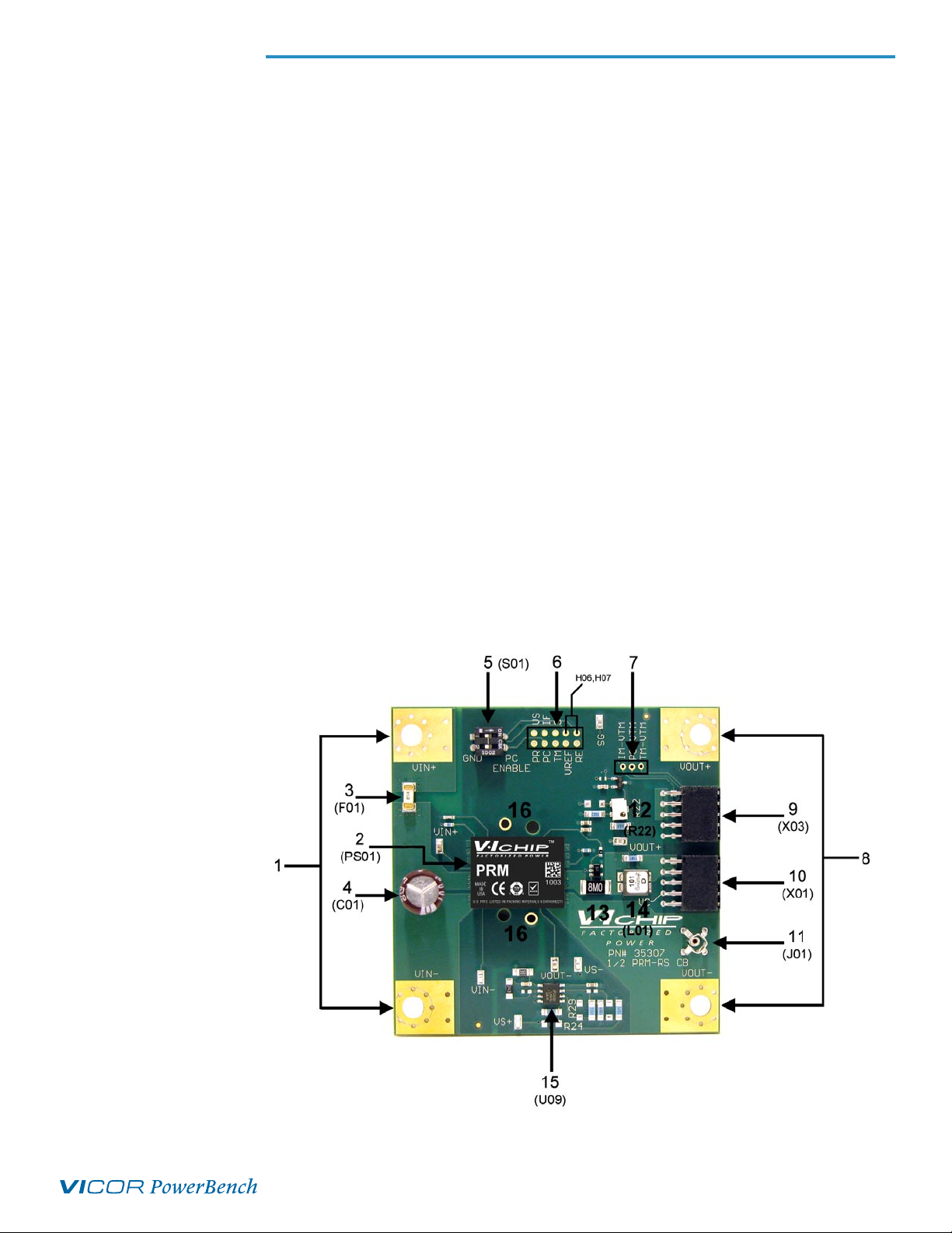
Figure 1
Board Description
Page 3

UG:008 vicorpower.com Applications Engineering: 800 927.9474 Page 3
3.1 General Components
Refer to Figure 1 and Figure 2:
1. Input Lugs: Sized for #10 hardware. Use these for making connections to the input source.
This board does not contain reverse polarity protection. Check for proper polarity before
applying power.
2. Half-chip PRM-RS module (PS01)
3. Input Fuse (F01): 10 A rated
4. Input Capacitor (C01): 100 µF, 63 V capacitor allows for stable operation with
most input sources.
5. Enable / Disable Switch (S01): Dual switch with the following functionality:
a. S01_1 (Top): Spare switch. Wired to H07 and H06 on the PRM signal test point header (#6)
to allow for extra functionality if needed. Both positions are open and not connected
anywhere else on the board.
b. S01_2 (Bottom): PC enable switch. When in the right position (ON), the PC pin will be
connected to –IN and the device will be disabled. When in the left position, PC will be
open, and the device will be enabled.
6. Signal Test Point Header: Dual row of plated through hole test points for making measurements
or connections to the signals labeled.
7. VTM
®
Signal Test Point Header: Plated through holes for measuring VTM signals returned
through connector X03. For use only with VTM Customer Boards containing dual headers.
8. Output Lugs: Sized for #10 hardware. Use these lugs to connect the output directly to the load
9. Signal Connector (X03): Used to transfer the VTM PC, IM, TM, and output sense signals
between the PRM and VTM Customer Boards. For use only with VTM Customer Boards
containing dual headers. Refer to Figure 2 for pinout.
10. Power / Signal Connector (X01): Used to transfer power (+/-Out) and VC to downstream VTM
Customer Board when used. For use with all VTM Customer Boards. Refer to Figure 2 for pinout.
11. Output Oscilloscope Probe Jack (J01): Used for making accurate scope measurements of the
output voltage (i.e. ripple). Remove scope grounding lead and insert probe directly into jack
ensuring a good connection between the jack and the probe ground barrel. Do not attempt to
install while power is applied. May not be compatible with all scope probes.
Figure 2
Power / Signal Connectors Pinout,
Front View
-OUT
-OUT
+OUT
-OUT
VC
+OUT
2
+OUT
+OUT
1
VC
-OUT
VS-
VS+
VTM -IN
NC
TM-VTM
NC
PC-VTM
IM-VTM
2
1
Power / Signal Connector (10)
X01
X03
Signal Connector (9)
Page 4

UG:008 vicorpower.com Applications Engineering: 800 927.9474 Page 4
12. Output Voltage Trim Pot (R22): 11 turn trim pot adjusts the output voltage by increasing or
decreasing the error amplifier reference voltage (V
REF). Turn clockwise to increase the output
voltage, and counterclockwise to decrease the output voltage. Adjustment slot is
1.5 mm (L) x 0.6 mm (W).
13. High Side Current Sense Circuit (R
08, Q02): Current sense shunt and IC monitor the output
current and provide feedback to the IF pin for current limit protection. Gain is typically 400
mV/A, and is set for appropriate current limit set point. IF signal can be monitored at the
Signal Test Point Header (#6) to provide approximate output current measurement, but should
not be used if accurate output current measurements are required (<10% error). Efficiency
measurements should always be performed using an external calibrated shunt.
14. Output Inductor (L01): 0.4 uH inductor provides high AC impedance between PRM
®
and VTM
®
(when used) to prevent high- frequency switching currents from circulating between devices.
15. Voltage Sense and Error Amplifier (U09A, U09B): Dual op amp provides voltage sensing and
error amplifier function. The customer board is nominally configured for local voltage sensing
at the PRM output. U09B can be re-configured as a differential amplifier to allow for
non-isolated remote sensing at the VTM output or load. This requires rework as described in
Section 8.3.
16. Push Pin Heat Sink and Grounding Clip Mounting Holes: Use these holes for installing the
optional push pin heat sink and grounding clips included with the board.
Use of a heat sink is highly recommended for appropriate cooling of the PRM.
3.2 Test Points
In addition to the Signal Test Point Headers (#6, #7), there are a number of surface mount test
points on the board with the following functions.
1. V
IN+, VIN- (TP01, TP03): Input voltage test points provide Kelvin connections to the input
leads. Use these test points for measuring the input voltage to avoid error due to interconnect
losses.
2. V
OUT+, VOUT- (TP04, TP05): Output voltage test points provide Kelvin connections to the
output leads. Use these test points for measuring the output voltage to avoid error due to
interconnect losses.
3. Signal Ground (TP01): Signal Ground (SG) test point is the ground reference for all control
circuitry.
4. VS+, VS- (TP10, TP11): +/- sense inputs to the differential amplifier when remote sense is
implemented. When used with a VTM Customer Board, the sense leads may be wired to the
VTM output voltage through X03 depending on which VTM board is used. If not, a twisted
pair of wires can be used to connect sense leads to the VTM board output from these test
points.
Page 5
UG:008 vicorpower.com Applications Engineering: 800 927.9474 Page 5
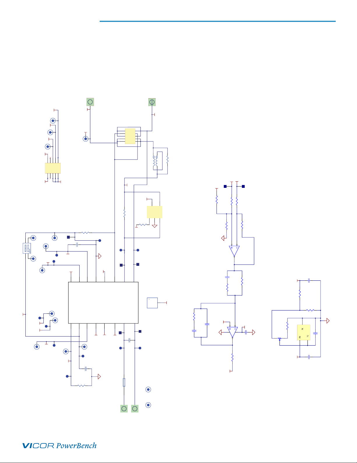
4.0 Schematic, Assembly and Bill of Material (BOM)
4.1 Schematic
Figure 3: Half-chip PRM-RS Customer Board Schematic
P01
TM-VTM
X03
IM-VTM
PC-VTM
H12
H11
H13
12345678910
32770
Vout+
Vout-
J0
VS- VS+
Vvtm_out-
R03
TP01
2
3
S01 SW DIP-2
1
4
H07 H06
H10
H08
VS
H09
TP18
TP13
C01
IF
NC4
15
16
VS
PO
TP16
GND
RE
11
14
12SG13
IM
RE
VC
PRM-RS
PC
TP19
H05
PC
PR
TP17
H04
1
RE
TM3NC4NC5NC
2
6
Vref
NC2
NC1
TP12
TM
H03
H01
PR
H02
TP15
C02
TP14
NC3
GND
R02
P02
8mR08
TP08
TP04
10
7
TP02
TP06
F01
VIN+
0
8
2
X01
PRMOUT
2512
+OUT
+IN
C05
29207-010
P03
91
7
56
3 4
1
32770
IF
9
–OUT
–IN
8
100u
VIN-
R09
TP09
TP05
TP03
TP07
P04
RE
Q02
OUT
1
0
PS01
FD2
FD1
0.1uH
L02
4
5
V+
HS01
FID UCIA L
FID UCIA L
2
GND
GND
GND
Vout-
4
VIN-
VIN+
3
1206
10
R10
SOT 23_5
VIN-
C07
R16
Vs-
Vs+
VS-
VS+
PRMOUT
TP10
TP11
54.9k
R29
R24
OPEN
OPEN
R40
1.24k
1.24k
R23
R30
GND
6
5
U09B
7
C10
R28
C13
Vref
R25
R31
R42
Vref
2
GND
3
48
U09A
1
R27
0 OHM
VS
GND
C11
R22
10k
C08
R32
1206
OPEN
U03
RE
3
C12
GND
T
IN
OUT2O
SOT 23_3
1
C14
GND
REF3312 Regulator (1.25V)
PR
Page 6
UG:008 vicorpower.com Applications Engineering: 800 927.9474 Page 6
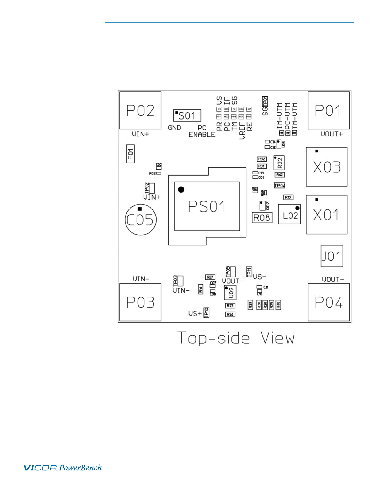
Figure 4
Half-chip PRM-RS
Customer Board
Assembly Drawing
4.2 Assembly Drawing
Page 7
UG:008 vicorpower.com Applications Engineering: 800 927.9474 Page 7
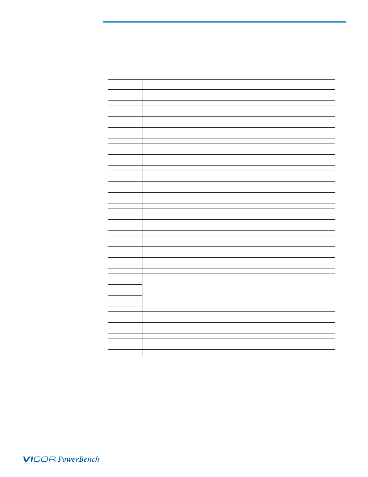
4.3 Bill of Materials
Ref. Des. Description Manufacturer
Manufacturer Part
Number
C01 Not Applied Not Applied Not Applied
C02 Not Applied Not Applied Not Applied
C05 CAP ALEL 100uF 20% 63 V 0.2 radial U. CHEMI-CON EKME630Ell101MJC5S
C07 CAP X7R 0.01uF 10% 100 V 0603 Generic Generic
C08 Not Applied Not Applied Not Applied
C10 Not Applied Not Applied Not Applied
C11 CAP X7R 0.01uF 10% 100 V 0603 Generic Generic
C12 CAP X7R 0.10uF 10% 16 V 0603 Generic Generic
C13 CAP X7R 0.22uF 10% 25 V 0603 Generic Generic
C14 Not Applied Not Applied Not Applied
F1 Littlefuse 10 Amp R451010.MRL Littlefuse 0451010.MRL
J01 Jack Vertical Mech Thru Hole Tektronix 131-5031-00
L02 Ind 0.1u/20%/20A dual 3026 Coilcraft SLC7530D-101MLC
PS01 Model Specific Vicor Model Specific
Q02 IC I Sense INA194 SOT23 5 TI INA194
R02 Not Applied Not Applied Not Applied
R03 RES 1K OHM 1W 1/10W 1% 0603 Generic Generic
R08 RES I Sense 8m OHM 1W 1% 2512 Generic Generic
R09 RES 0 OHM Jumper 1A 0603 Generic Generic
R10 RES 10 OHM 1/4W 1% 1206 Generic Generic
R16 RES 17.4K OHM 1/4W 1% 1206 Generic Generic
R22 RES TRIM POT 10K OHM 1/4W 10% SMD Murata PVG5A103C03R00
R23 RES 1.24K OHM 1/4W 1% 1206 Generic Generic
R24 Not Applied Not Applied Not Applied
R25 Not Applied Not Applied Not Applied
R27 RES 0 OHM 1/8W 5% 1206 Generic Generic
R28 RES 1K OHM 1/4W 1% 1206 Generic Generic
R29 Not Applied Not Applied Not Applied
R30 RES 1.24K OHM 1/4W 1% 1206 Generic Generic
R31 RES 10K OHM 1/4W 1% 1206 Generic Generic
R32 Not Applied Not Applied Not Applied
R40 RES 54.9K OHM 1/4W 1% SMD 1206 Generic Generic
R42 RES 4.99K OHM 1/4W 1% 1206 Generic Generic
S01 SW DIP SPST 2 POS C&K SD02H0B
TP01
TP02
TP03
TP04 Test Point, Surface Mount Keystone 5017
TP05
TP10
TP11
U03 IC VREF 1.25V REF3312 SOT23 3 TI REF3312
U09 IC DUAL OPAMP LM6142AIM 8PIN SO National LM6142AIM
X01
X03
CONN 10POS 90° Thru-Hole Female 0.100SPC Sullins PPTC052LJBN-RC
ACCESSORY 1 HS XF 11mm Half VIC Vicor 32784
ACCESSORY 2 Clip Heat sink Grounding Vicor 33855
ACCESSORY 3 CONN 10POS Header STR M-M 3A/0.100 Sullins PEC05DABN
ACCESSORY 4 Push-Pin White 0.063” Vicor 34141
Table 1
Half-chip PRM-RS Customer Board
BOM
Page 8

UG:008 vicorpower.com Applications Engineering: 800 927.9474 Page 8
5.0 VTM®Customer Boards
The half-chip PRM-RS Customer Board is designed to work with all types of VTM Customer Boards
to facilitate testing of virtually any PRM
®
/VTM combination. Note that there are currently two basic
types of VTM Customer Boards. Both board types share many common features, including input
capacitance, output capacitance, and various test points. The main difference between the two board
types is the number of connectors. Before configuring a PRM/VTM setup, the user should identify
which type of VTM board is being used.
5.1 VTM Customer Board Type A (Single Connector)
The VTM Customer Board Type A contains a single power / signal header designed to mate with
only X01 on the half-chip PRM-RS Customer Board. The PRM output voltage, and VC signal are
transferred through this header when connected to a PRM Customer Board.
VTMTM CUSTOMER BOARD
TYPE A
-IN
-IN
-IN
-IN
+IN
+IN +IN
+IN
VC
VC
Figure 5
VTM Customer Board Type A
Figure 6
VTM Customer Board Type A
Connector Pinout (Front View)
Page 9

UG:008 vicorpower.com Applications Engineering: 800 927.9474 Page 9
5.2 VTM®Customer Board Type B (Dual Connectors)
The VTM Customer Board Type B contains dual connectors designed to mate with both X01 and
X03 on the half-chip PRM-RS Customer Board. The additional connector is used to transfer VTM
signal pins, as well as the VS+ and VS- signals between boards. The VS+ and VS- signals are tied
directly to the VTM output and can be used for implementing remote sense as described
in a later section.
Figure 7: VTM Customer Board
Type B
VTMTM CUSTOMER BOA
TYPE B
Power / Signal Connecto
VTM
TM
CUSTOMER BOARD
TYPE B
Signal Connector
-IN
-IN
-IN
-IN
+IN
+IN +IN
+IN
VC
VC
NC
NC
VS+
VS-
IM-VTM
PC-VTM
TM-VTM
VTM -IN
Figure 8: VTM Customer Board
Type B
Connector Pinout (Front View)
Page 10

UG:008 vicorpower.com Applications Engineering: 800 927.9474 Page 10
6.0 Recommended Test Equipment
The following is a list of recommended test equipment. Output load current, and voltage ratings are
a function of the VTM
®
selected (if used).
1. DC Power Supply: 0 – 100 V, 500 W minimum.
a. Set Overvoltage Protection (OVP) based on absolute maximum rating of PRM
®
.
2. Load: Rated appropriately based on output voltage, current, and power requirements. Electronic
load, 0 to 100 V, 130 A minimum recommended.
3. DMM(s).
4. Oscilloscope + Probe(s).
5. Interconnect cables and fastening hardware.
6. Calibrated input and output shunts, appropriately rated.
7. Trim Pot screwdriver
8. Fan
9. Data sheets for requisite PRM and VTM devices used.
10.Safety glasses.
7.0 Push Pin Heat Sink Installation
Each PRM and VTM Customer Board comes with its own heat sink and push pins for installation.
Before testing, it is highly recommended that heat sinks be installed in the appropriate location for
each board. When installing the push pin heat sink, use caution not to exceed the maximum
compressive on the device listed in the data sheet.
8.0 Test Configurations
The half-chip PRM-RS Customer Board is designed to work in a number of different configurations as
described in the following section. The scope of this document is limited to describing a single PRM
Customer Board as a stand-alone or connected to a single VTM Customer Board. Other
configurations may be possible, though they cannot be guaranteed to have stable operation with the
components designed onto the board. If testing is to be performed outside of the recommended
configurations, the design should be evaluated to determine if changes to any of the onboard
components are necessary.
8.1 PRM Stand-alone Operation
In this configuration, the PRM output voltage is sensed through the divider formed by R40 and
R23. U09B is configured as a buffer as illustrated in Figure 9, and provides the sense voltage to
the error amplifier (U09A). R24, and R29 are left open, reserved for differential sensing. R40 is
set to limit the upper trim range based on a maximum reference voltage of 1.25 V.
1.24k
R30
1.24k
R23
Vs-
Vs+
PRMO UT
VS+
VS-
TP10
TP11
R40
R24
R29
6
5
7
U09B
GND
OPEN
OPEN
54.9k
Figure 9: Local Sense
Configuration
Page 11

UG:008 vicorpower.com Applications Engineering: 800 927.9474 Page 11
8.1.1 PRM®Stand-alone Operation Setup
This is the nominal configuration, and requires no rework to implement. If the board has
been modified, restore to its original configuration.
1. Solder test leads to signals on the test point header that will be measured.
2. Connect input source to the input lugs. Verify proper polarity. Set to 0 Volts or OFF before
connecting.
3. Connect output to load using the output lugs. Set load to 0 Amps or OFF.
4. Insert oscilloscope probe into J01 if used.
5. Connect DMM to the output test points (V
OUT+, VOUT-) and to any other signals to be
measured.
6. Set PC Enable Switch (S01_2) to the left position.
7. Apply nominal input voltage.
8. Measure output voltage and verify operation.
9. Use the output voltage trim pot (R
22) to adjust the output to the desired level.
10. Apply 100% load, and verify full load operation.
11. Turn off load and power. Proceed to following sections for detailed test procedure.
8.2 PRM – VTM®Operation, Local Sense
In this configuration, the PRM-CB and VTM-CB are connected together to form a PRM/VTM pair
and regulation is performed at the PRM output. Load regulation will be degraded due to the VTM
output resistance. Tighter regulation can be achieved by implementing non-isolated remote sense
as described in Section 8.3.
8.2.1 PRM – VTM Local Sense Setup
Local sensing is the nominal configuration of the customer board and requires no rework to
implement. If the board has been modified, restore it to its original configuration.
1. Solder leads to any signals on the test point header to be measured.
2. Identify the type of VTM Customer Board to be used (Type A, or Type B).
a. Type A: Install single male-to-male header to X01 only.
b. Type B: Install dual male-to-male headers on X01 and X03.
3. Connect desired VTM board referring to Figure 11 or Figure 12.
4. Connect input source to the input lugs. Verify proper polarity.
Set to 0 Volts or OFF before connecting.
5. Connect VTM output to load using the output lugs. Set load to 0 Amps or OFF.
6. Insert oscilloscope probe into VTM output probe jack.
7. Connect DMM to the VTM output test points and to any other signals to be measured.
8. Set PC Enable Switch (S01_2) to the left position.
9. Apply nominal input voltage.
10. Measure VTM output voltage and verify operation.
11. Use the output voltage trim pot (R
22) to adjust the output to the desired level.
a. Do not trim below the minimum input voltage of the VTM used.
12. Apply 100% load, and verify full load operation.
13. Turn off load and power. Proceed to following sections for detailed test procedure.
Page 12

UG:008 vicorpower.com Applications Engineering: 800 927.9474 Page 12
8.3.1 PRM – VTM Remote Sense Setup
This is NOT the nominal configuration of the customer board and requires rework to implement.
1. Determine the maximum desired VTM output trim voltage (R
22 fully clockwise).
2. Use Equation 1 to select the appropriate value for R
24/R29. Obtain the closest 1% standard
value, size 1206 resistors for installation.
3. Remove R
40.
4. Install R
24 and R29 in the appropriate positions
5. Determine the type of VTM Customer Board to be used.
a. Type A:
i. Install single male-to-male header to X01 only.
ii. Connect PRM and VTM Customer Boards together as illustrated in Figure 11.
iii.Connect the VS+ test point to the VTM +OUT test point, and VS- test point to the VTM
–OUT test point through a twisted pair of wire
b. Type B:
i. Install dual male-to-male headers to X01 and X03
ii. Connect PRM and VTM Customer Boards together as illustrated in Figure 12.
iii.Verify connection from VS+ to VTM +OUT, and VS- to VTM -OUT
6. Connect a jumper between VTM –OUT and VTM –IN
7. Connect input source to the input lugs. Verify proper polarity. Set to 0 Volts or OFF before
connecting.
8. Connect VTM output to desired load using the output lugs. Set load to 0 Amps or OFF.
1.24k
R30
1.24k
R23
Vs-
Vs+
PRMO UT
VS+
VS-
TP10
TP11
R40
R24
R29
6
5
7
U09B
GND
OPEN
Figure 10: Remote Sense
Configuration
Equation 1
Where: VOUT_SET(MAX) is the maximum VTM output trim voltage
8.3 PRM – VTM®Operation, Non-isolated Remote Sense
In this configuration, the PRM and VTM Customer Boards are connected together to form a
PRM
®
/VTM pair and regulation is performed at the VTM output. U09B is configured as a differential
amplifier with a gain set for the appropriate output voltage. R24,and R29 set the gain and
limit the maximum VTM output voltage based on Equation 1 assuming the trim pot (R22)
is fully clockwise.
Page 13

UG:008 vicorpower.com Applications Engineering: 800 927.9474 Page 13
9. Insert oscilloscope probe into VTM®output probe jack.
10. Connect DMM to the VTM output test points and to any other signals to be measured.
11. Set PC Enable Switch (S0_2) to the left position.
12. Apply nominal input voltage.
13. Measure VTM output voltage and verify operation.
14. Use the output voltage trim pot (R
22) to adjust the output to the desired level.
a. Do not trim below the minimum input voltage of the VTM used.
15. Apply 100% load, and verify full load operation.
16. Turn off load and power. Proceed to following sections for detailed test procedure.
Figure 11: Half-chip PRM-RS
Customer Board connection to
VTM Customer Board Type A
Figure 12: Half-chip PRM-RS
Customer Board Connection to
VTM Customer Board Type B
Page 14

UG:008 vicorpower.com Applications Engineering: 800 927.9474 Page 14
9.0 Test Procedure
Once the board has been setup and verified to be functional, it can now be used to characterize the
behavior, and performance of the selected configuration. Some typical tests are outlined below.
9.1 Efficiency vs. Line / Load (Ambient)
1. Connect input source through calibrated input shunt noting the value. Set to 0 Volts or OFF.
2. Connect output to load through calibrated output shunt noting the value.
Set to 0 Amps or OFF.
3. Connect DMMs to measure input voltage, output voltage, input shunt voltage, and output
shunt voltage. Use Kelvin test points for input, output, and shunt voltage measurements.
4. Turn on fan for cooling. Make sure heat sink is installed.
5. Set PC enable switch to the Left position.
6. Apply desired input voltage and load.
7. Quickly record DMM measurements to avoid heating.
i. GPIB control recommended for simultaneous DMM measurement recording.
8. Turn off input source and load. Allow device to cool to ambient temperature.
9. Repeat for all desired test conditions.
i. GPIB control recommended for line/load sweeps.
10.Use data to calculate efficiency.
9.2 Output Ripple vs. Load
1. Connect input source and load. Set to OFF.
2. Insert oscilloscope probe into output probe jack.
3. Set oscilloscope:
i. AC coupling 1 MΩ, 20 MHz bandwidth.
ii. Time scale: 1 µsec / div
iii. Voltage scale: 200 mV / division
4. Turn on fan for cooling.
5. Apply input voltage.
6. Apply load.
7. Record oscilloscope waveform. Use cursors to measure pk-pk ripple. Adjust scales as necessary.
8. Repeat for all desired conditions.
9.3 Startup Timing, Application of Input
1. Connect input source and load. Set to OFF.
2. Connect oscilloscope probes to V
IN, VOUT, and any other signals to be measured
3. Set scope voltage, and time scales appropriately.
i. 20 msec / div recommended time scale
ii. Trigger on positive edge of V
IN
4. Apply desired startup load
5. Set input source to ramp from 0 to V
IN(NOM).
i. Ensure that the slew rate is within acceptable limits
6. Capture waveform. Adjust scales as necessary.
Page 15

UG:008 vicorpower.com Applications Engineering: 800 927.9474 Page 15
9.4 PC Enable / Disable Timing
1. Connect input source and load. Set to OFF.
2. Set PC enable switch (S01-2) to the right position to disable the PRM
®
.
i. PC should be connected to SG.
3. Connect scope probes to PC, V
OUT, and any other signals to be measured.
4. Set scope scales appropriately.
i. 1 msec / div recommended.
ii. Trigger on positive edge of PC.
5. Apply desired startup load.
6. Apply nominal input voltage (V
IN(NOM)).
i. Verify unit is disabled.
7. Move S01_2 to the left position to enable the device.
8. Record Enable waveform. Adjust scales as necessary.
9. Trigger on negative edge of PC.
10.Move S01_2 to the Right position to disable the device.
11.Record Disable waveform. Adjust scales as necessary.
12.Monitor for switch bounce. Repeat measurement or adjust setup as necessary.
9.5 Current Limit
Note: In order for this test to be performed properly, a resistive load must be used. This
includes an electronic load set to constant resistance mode. Be cautious of potential load
interactions when using electronic loads. If the output voltage or current begin to
oscillate, repeat the test with a passive resistive load.
1. Apply input source and load. Set to OFF.
2. If using an electronic load, change to Constant Resistance mode.
3. Connect DMMs to measure V
OUT, IF, and any other signals to be measured.
i. Use electronic load reading, clamp on DC meter to measure approximate output current or
calibrated shunt for more accurate measurement.
4. Set S01_2 to Left position to enable the device.
5. Apply input voltage. Verify output is present.
6. Enable load. Gradually ramp up current (decrease resistance) until current limit threshold is
reached.
i. Current will remain at maximum, output voltage will fold back.
Page 16

UG:008 vicorpower.com Applications Engineering: 800 927.9474 Page 16
10.0 Advanced Modifications
10.1 Stability, Bandwidth and Transient Response
The nominal compensation of the half-chip PRM-RS Customer Board is set to provide relatively low
bandwidth in order to ensure stability under all of the recommended configurations. The closed
loop frequency response varies as a function of line, load, trim, and output capacitance. Refer to
the PRM
®
data sheet for a detailed description and AC model. Adding additional capacitance to the
output of the PRM or VTM
®
Customer Board may result in instability. When testing transient
response, it is important for the user to understand that response is a function of compensation
which should be optimized based on the end requirements for best performance. An example
transient response waveform, taken with a passive resistive load, is shown below. As illustrated, the
recovery time is on the order of 400 µsec. It should be noted that with control loop optimization,
faster transient response recovery times are possible.
10.1.1 Compensation Adjustment
The sense and compensation circuit is shown below. Refer to the BOM (4.3) for component
values. If higher bandwidth, faster transient response, and/or operation outside of the
recommended configurations are desired, the user may adjust the compensation, referring to
the appropriate PRM data sheet for guidelines. This type of tuning is highly recommended and
generally requires the use of a network analyzer to measure the closed loop response. Stability
must be verified across all line, load, and trim conditions. Typically maximum crossover
frequency will occur at full load, and minimum crossover frequency will occur at minimum load.
Examples of closed loop response plots are illustrated below.
Figure 13: Example
PRD48BH480T200A00
(VIP0100THJ-CB) transient response
PRD48BH480T200A00 +
V048F480T006-CB, Remote Sense
Configuration
Page 17

UG:008 vicorpower.com Applications Engineering: 800 927.9474 Page 17
Figure 14
Sense and Compensation Components
Figure 15
PRD48BH480T200A00 +
V048F480T006-CB Closed Loop
Response, Differential Sense, 48 V
OUT,
0.2 A, Resistive Load
Figure 16
PRD48BH480T200A00 +
V048F480T006-CB Closed Loop
Response, Differential Sense, 48VOUT,
4 A, Resistive Load
C07
R16
C08
R40
R24
R29
PRMOUT
TP10
TP11
Vs+
VS+
VS-
Vs-
GND
Vref
PR
R27
0 OHM
48
3
1
U09A
2
C11
VS
GND
R25
C10
7
R28
U09B
GND
5
6
R30
R23
1.24k
1.24k
Gain
Gain
Phase
(Hz)
Phase
(Hz)
Page 18

UG:008 vicorpower.com Applications Engineering: 800 927.9474 Page 18
10.2 Current Limit Adjustment
The current limit set point is a function of the current sense amplifier gain, the shunt resistor, and
the internal current limit threshold of the PRM
®
. The onboard current sense IC and shunt have a
typical combined gain of 400 mV/A. The gain of the current sense IC (Q
02) is fixed at 50 V/V, and
the IF current limit threshold is fixed at 2.0V. The current sense shunt (R
08) can be changed per
Equation 2 in order to adjust the current limit. Once the value has been calculated, obtain the
closest 1% standard value, size 2512 resistor and replace R
08.
10.3 Trim Range Adjustment
The trim range is set by the reference voltage network shown below. The half-chip PRM-RS
Customer Board is nominally configured for a 20 V to 55 V trim range. Any operation outside of
the nominal trim range may require adjustments to the compensation.
Assuming local sense is implemented, the output voltage is defined by Equation 3. Referring to
Figure 17, the output of U
03 is 1.25 V. When R22 is fully clockwise, the U03 output voltage will be
applied directly to V
REF resulting in the maximum reference voltage. This, in combination with the
voltage sense gain will determine the maximum output voltage. As R
22 is turned counter
clockwise, R
22 and R42 form a divider which limits the minimum reference voltage.
In order to change the upper trim range, adjust the voltage sense gain (R
40) based on a maximum
reference voltage of 1.25 V. In order to change the lower trim range, use Equation 3 to determine
the minimum reference voltage required and adjust R
42 appropriately. Before making adjustments
to the trim range, refer to the data sheet to ensure that the device will operate outside of its
rated limits.
V
IF_IL is the IF current limit threshold (2.0 V)
I
LIMIT(SET) is the desired current limit set point
G
CS is the current sense amplifier (QO2) gain (50 V/V)
Equation 2
Equation 3
(local sense only)
Page 19

vicorpower.com Applications Engineering: 800 927.9474 Rev 1.2 Page 19
09/2014
GND
RE Vref
C14
R42
REF3312 Regulator (1.25V)
SOT 23_3
GND
3
IN
1
OUT
2
N
D
I
N
O
U
U03
C12
C13
R31
1206
OPEN
R32
10k
R22
4.99 k
10 k
Figure 17
Reference Circuit
11.0 Conclusion
The half-chip PRM-RS Customer Board is a flexible tool which allows users to implement and perform
basic testing on a very wide range of configurations, including PRM
®
-VTM®combinations. This User
Guide covers some basic and advanced topics; however, it cannot describe every scenario. If additional
information is required, please contact Vicor Applications Engineering.
Technical advice furnished by Vicor is provided as a free service, with the intent
to facilitate successful implementation of Vicor Products. Vicor assumes
no obligation or liability for the advice given or results obtained.
All such advice given and accepted is at user's risk.
Go to: http://www.vicorpower.com/contact-us for ordering information and application
support.
G
 Loading...