

VESTEL DVD5500 Service Manual

DVD5500
DVD PLAYER
SERVICE MANUAL

ENERAL DESCRIPTION
1. G
1.1 MT1379
The MT1379 Progressive Scan DVD-Player Combo Chip is a single-chip MPEG video
decoding chip that integrates audio/video stream data processing, TV encoder, four video DACs
with Macrovision. copy protection, DVD system navigation, system control and housekeeping
functions.
The features of this chip can be listed as follows:
General Features:
• Progressive scan DVD-player combo chip
• Integrated NTSC/PAL encoder.
• Built-in progressive video output
• DVD-Video, VCD 1.1, 2.0, and SVCD
• Unified track buffer and A/V decoding buffer.
• Direct interface of 32-bit SDRAM.
• Servo controller and data channel processing.
Video Related Features:
• Macrovision 7.1 for NTSC/PAL interlaced video.
• Simultaneous composite video and S-video outputs, or composite and YUV outputs, or
composite and RGB outputs.
• 8-bit CCIR 601 YUV 4:2:2 output.
• Decodes MPEG video and MPEG2 main profile at main level.
• Maximum input bit rate of 15Mbits/sec
Audio Related Features:
• Dolby Digital (AC-3) and Dolby Pro Logic.
• Dolby Digital S/PDIF digital audio output.
• High-Definition Compatible Digital. (HDCD) decoding.
• Dolby Digital Class A and HDCD certified.
• SRS TrueSurround ..
• CD-DA.
• MP3.
2

1.2 M
OSD, MPEG stream and video buffer memory for a DVD player. The maximum amount of
memory supported is 16 MB of Synchronous DRAM (SDRAM). The memory interface is
configurable in depth to support 128-Mb addressing. The memory interface controls access to
both external SDRAM memories, which can be the sole unified external read/write memory acting
as program and data memory as well as various decoding and display buffers.
1.3 D
many types of DVD loaders. These interfaces meet the specifications of many DVD loader
manufacturers.
1.4 F
controller chip, (uPD16311). The MT1379 controls the uPD16311 using several control signals,
(clock, data, chip select). The infrared remote control signal is passed directly to the MT1379 for
decoding.
1.5 R
A typical rear panel is included in the reference design. This rear panel supports:
- Six channel or two channel audio outputs
- Optical and coax S/PDIF outputs.
- Composite, S-Video, and SCART outputs
EMORY
1.2.1
The MT1379 provides a glueless 16-bit interface to DRAM memory devices used as
RIVE INTERFACES
The MT1379 supports the DV34 interface, and other RF and servo interfaces used by
RONT PANEL
The front panel is based around an Futaba VFD and a common NEC front panel
EAR PANEL
SDRAM Memory Interface
The six-video signals used to provide CVBS, S-Video, and RGB are generated by the MT1379’s
internal video DAC. The video signals are buffered by external circuitry.
Six channel audio output by the MT1379 in the form of three I
S/PDIF serial stream is also generated by the MT1379 output by the rear panel. The six channel
audio DACs (AK4356,PCM1606) are used for six channel audio output with MT1379, and
similarly AK4382A ,CS4392 Audio DACs are used for two channel audio output with MT1379.
2
S (or similar) data streams. The
3
YSTEM BLOCK DIAGRAM and
2. S
MT1379 P
IN DESCRIPTION
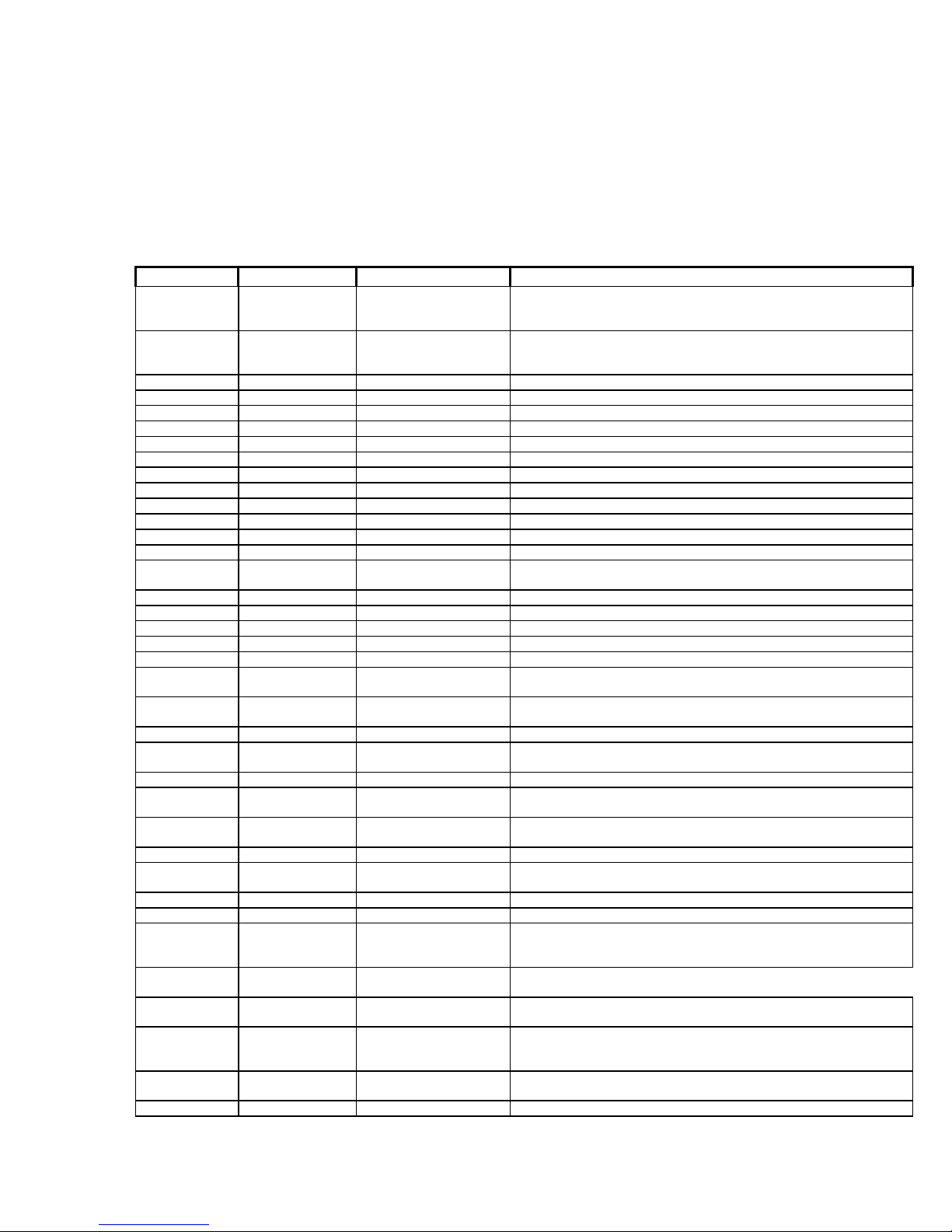
2.1 MT1379 PIN DESCRIPTION
SYMBOL TYPE PIN NUMBERS DEFINITION
DVSS Ground 115,125,135,145 Ground pin for internal digital circuitry
IREF Analog Input 1 Current for data PLL. Connect an external 100K
PLLVSS Ground 2 Ground pin for PLL and analog circuitry
LPIOP Analog Output 3 Positive output for low pass filter(LFP)
LPION Analog Output 4 Negative output for LFP
LPFON Analog Output 5 Negative output of loop filter amplifier(LFA)
LPFIP Analog Input 6 Positive input of LFA
LPFIN Analog Input 7 Negative input of LFA
LPFOP Analog Output 8 Positive output of LFA
JITFO Analog Output 9 RF jitter meter output
JITFN Analog Input 10 Negative input of the operational amplifier for RF jigger meter
PLLVDD3 Power 11 3.3V power pin for data PLL and related analog circuitry
FOO Analog Output 12 Focus servo output. PDM output of focus servo compensator
TRO Analog Output 13 Tracking servo output. PDM output of tracking servo compensator
TROPENPWM Analog Output 14 for TRWMEN27hRW2=1 or is digital output for TRWMEN27hRW2=0
PWMOUT1-2 Analog Output 15-16 1st and 2nd general PWM output.
DVDD2 Power 17,42,72,82,120,140,182 2.5V power pin for internally fully digital circuitry.
DMO Analog Output 18 Disk motor control output. PWM output.
FMO Analog Output 19 Feed motor control PWM output.
FG Input 21 Motor Hall sensor input
HIGHA0-5 Inout 2~16MA,SR
PU
HIGHA6-7 Inout 2~16MA,SR
PU
AD7-4 Inout 2~16MA,SR 31-34 Microcontroller address/data 7-4
DVDD3 Power 35,66,97,111,130,150,185
AD3-0 Inout 2~16MA,SR 36-39 Microcontroller address/data 3-0
IOA0-1 Inout 2~16MA,SR
PU
IOA2-7 Inout 2~16MA,SR
PU
A16-17 Output 2~16MA,SR 49-50 Flash adress 16-17
IOA18-20 Inout 2~16MA,SR
SMT
APLLVSS Ground 54 Ground pin for audio clock circuitry
APLLVDD3 Power 55 3.3V power pin for audio clock circuitry
ALE Inout
2~16MA,SR,PU,S
MT
IOOE# Inout 2~16MA,SR
SMT
IOWR# Inout
2~16MA,SR,SMT
IOCS# Inout
2~16MA,SR,PU,S
MT
UP1_2-6,7 Inout
4MA,SR,PU,SMT
UP3_0-1 Inout 68,69 Microcontroller port 3-0,3-1
20,28,60,77,92,102
178,189
Current reference input. It generates reference
Resistor to this pin and PLLVSS.
Tray open output,controlled by microcontroller. This is PWM output
22-27 Microcontroller address 8-13
29-30 Microcontroller address 14-15
3.3 power pin for internal digital circuitry
,192
40-41 Microcontroller adress 0-1/IO
43-48 Microcontroller adress 2-7/IO
51-52 Flash adress 18-19
56 Microcontroller address latch enable
57 Flash output enable, active low I/O
58 Flash write enable, active low/IO
59 Flash chip select,active low/IO
61-65,67 Microcontroller port 1-2…1-7
4
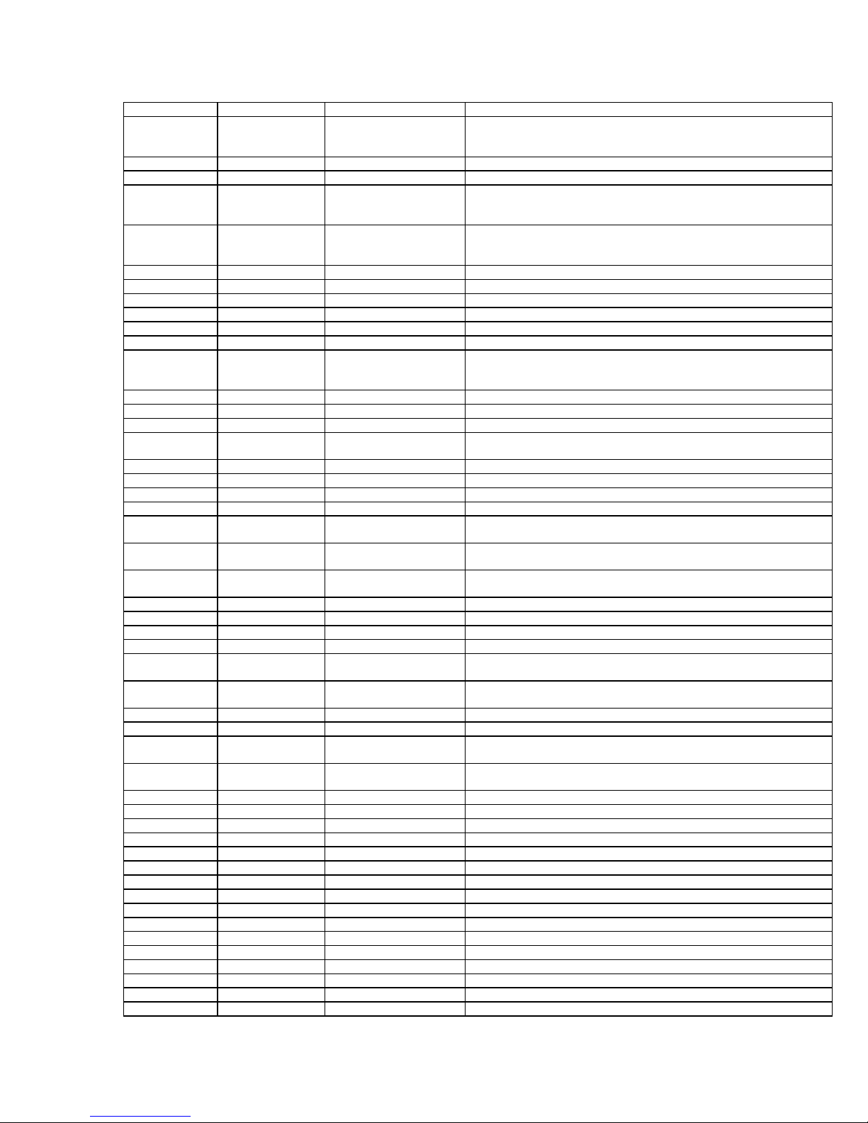
INT0# Inout
IR Input SMT 71 IR control signal input
UP3_4,5 Inout 73-74 Microcontroller port 3-4,3-5
UWR# Inout
URD# Inout
RD7-4,3-0 DRAM data 7-4,3-0 78-81,83-86 DRAM data 7-4,3-0
RWE# Output 2~16MA,SR 87 DRAM write enable, active low.
CAS# Output 2~16MA,SR 88 DRAM column adress strobe,active low
RAS# Output 2~16MA,SR 89 DRAM row adress strobe,active low
RCS# Output 2~16MA,SR 90 DRAM chip select, active low
BA0 Output 2~16MA,SR 91 DRAM bank adress 0
RD15-12,11-8 Inout
CLK Output 2~16MA,SR 103 DRAM clock
CLE Output 2~16MA,SR 104 DRAM clock enable
RA11 Output 2~16MA,SR 105 DRAM adress bit 11 or serial data 3(channel 7/8)
RA9,8,7,6-
4,10,0-3
DMVDD3 Power 108 3.3V Power pin for DRAM clock circuitry
DMVSS Ground 109 Ground pin for DRAM clock circuitry
DQM1,0-3,2 Output 2~16MA,SR 116,117-136,137 Mask for DRAM input/output byte 1,0
BA1 Output 2~16MA,SR 118 DRAM bank address 0
RD31-28,27-24 Inout 2~16MA,SR
RD23-22,21-18 Inout 2~16MA,SR
RD17-16 Inout 2~16MA,SR
ABCK Output 4MA 148 Audio bit clock
ALRCK Inout 4MA,PD,SMT 149 Audio L/R channel clock,Trap value in power-on reset 1:ext. 0:int.
ACLK Inout 4MA 151 Audio DAC master clock(384/256 audio sample frequency)
MC_DATA Input 152 Microphone serial input
SPDIF Output 2~16MA,SR
ASDATA0 Inout 4MA PD SMT 154 (1)Audio serial data 0(L/R)(2)Trap value in power on reset 1:factory test
ASDATA1 Inout 4MA PD SMT 155 Audio serial data 1(surround L/R),Trap value in power-on reset
ASDATA2 Inout 4MA PD SMT 156 Audio serial data 2(center/left),Trap value in power-on reset
ASDATA3 Inout 4MA PD SMT 157 Audio serial data 3(surround L/R),Trap value in power-on reset,videoin
ASDATA4 Inout 4MA PD SMT 158 Audio serial data 4(center/left),Trap value in power-on reset,videoin
DACVDDC Power 159 3.3V power pin for VİDEO DAC circuitry
VREF Analog input 160 Bandgap refernce voltage
FS Analog Output 161 Full scale adjustment
YUV0/CIN Output 4MA,SR 162 Video data output bit 0/Compensation capacitor
DACVSSC Ground 163 Ground pin for VIDEO DAC circuitry
YUV1/C Output 4MA,SR 164 Video data output bit 1/Compensation capacitor
DACVDDB Power 165 3.3V power pin for VİDEO DAC circuitry
YUV2/Y Output 4MA,SR 166 Video data output bit 2/ Analog Y output
DACVSSB Ground 167 Ground pin for VIDEO DAC circuitry
YUV3/CVBS Output 4MA,SR 168 Video data output bit 3/ Analog composite output
DACVDDA Power 169 3.3V power pin for VİDEO DAC circuitry
YUV4/G Output 4MA,SR 170 Video data output bit 4/Green or Y
DACVSSA Ground 171 Ground pin for VIDEO DAC circuitry
YUV5/B Output 4MA,SR 172 Video data output bit 5/Blue or CB
YUV6/R Output 4MA,SR 173 Video data output bit 5/Red or CR
ICE Input PD,SMT 174 Microcontroller ICE mode enable
4MA,SR,PU,SMT
2~16MA,SR,PU,S
MT
2~16MA,SR,PU,S
MT
2~16MA,SR,PU,S
MT
2~16MA,SR,PU/PD
,SMT
Output 2~16MA,SR 106,107,110,112-
PU/PD SMT
PU/PD SMT
PU/PD SMT
:ON/OFF
70 Microcontroller interrupt 0, active low
75 Microcontroller write strobe,active low
76 Microcontroller write strobe,active low
93-96,98-101 DRAM data 15-12,11-8
DRAM adresses
114,119,121-124
126-129,131-134 DRAM corresponding data
138-139,141-144 DRAM data 23-22,21-18/Videoin Data PortA 7-6,5-2
146-147 DRAM data 17-16/Videoin Data PortA 1-0
153 SPDIF output
mode 0:normal mode
data portb 1
data portb 2
5
 Loading...