

Page 1

DVD4250D
DVD PLAYER
SERVICE MANUAL
1
Page 2

ENERAL DESCRIPTION
1. G
1.1 ES66x8
The ES66x8 Vibratto II processor is a hig hly integrated single -chip DVD solution that integrates read
channel, ECC, Servo DSP, MCU, and MPEG-2/MPEG-4/DivX decoder that has a state-of-the-art 480p/576p
progressive-scan video feature to provide brilliant and sharp, flicker-free video output to the display, and with
built-in gamma correction and S/PDIF input and output support. The 66x8 performs audio/video stream data
processing, TV encoding, Macrovision copy protection, DVD system navigation, system control, and
housekeeping functions.
The Vibratto II DVD processor is built on the ESS proprietary dual CPU Programmable Multimedia
Processor (PMP) core consisting of 32 -bit RISC and 64-bit DSP processors and offers the best DVD feature set.
These features can be listed as follows:
General Features:
− Single -chip DVD processor incorporating all front-end and back-end functions.
− Unified memory architecture.
− Built-in ADCs and DACs for servo control signals .
− DVD-Video, DVD-VR, VCD 1.1 and 2.0 and SVCD
− Proven ECC, EFM/EFM+ demodulation, and EDC circuit.
− Direct interface of 16-bit DRAM up to 128-Mb capacity.
− Direct interface of 8- or 16-bit SDRAM up to 128-Mb capacity.
− Direct interface for up to 4 banks of 8-bit EPROM or Flash EPROM for up to 4 MB per bank.
− Direct interface to the ES6603 servo AFE chip.
Video Related Features:
− Integrated NTSC/PAL encoder with pixel-adaptive de-interlacer and five 10-bit 54 MHz video DACs .
− DivX and MPEG-4 Advanced Simple Profile at full screen.
− Media playback with CD-ROM, CD-R/RW, DVD-R/RW and DVD+R/RW.
− Macrovision 7.1 for NTSC/PAL interlaced video.
− Macrovision NTSC/PAL (480p/576p) progressive scan video.
− Simultaneous composite, S-video and YUV outputs.
− CCIR656/601 YUV 4:2:2 output.
− OSD controller supports 256 colors in 8 degrees of transparency.
− JPEG digital photo CD support ( Kodak Picture CD and Fujifilm FujiColor CD ).
2
Page 3

Audio Related Features:
− Full DVD-Audio support including MLP and LPCM decode, CPPM decryption, and watermark detection.
− Up to 7.1 channel audio outputs .
− Bass management.
− Dolby Digital ( AC-3 ), Dolby Pro Logic, and Pro Logic II.
− DTS surround ( ES6698 only ).
− S/PDIF digital audio input and output.
− SRS TruSurround.
− Professional karaoke with full scoring scheme.
1.2 MEMORY
1.2.1 System SRAM Interface
The system SRAM interface controls access to optional external SRAM, which can be used for RISC
code, stack, and data. The SRAM bus supports four independent address spaces, each having programmable bus
width and wait states. The interface can support not only SRAM, but also
ROM/EPROM and memory -mapped I/O ports for standalone applications are supported.
1.2.2 DRAM Memory Interface
The Vibratto II provides a glueless 16-bit interface to DRAM memory devices used as video memory
for a DVD player. The maximum amount of memory supported is 16 MB of Synchronous DRAM (SDRAM).
The memory interface is configurable in depth to support 12 8-Mb addressing. The memory interface controls
access to both external SDRAM or EDO memories, which can be the sole unified external read/write memory
acting as program and data memory as well as various decoding and display buffers.
1.3 FRONT PANEL
The front panel is based around an Futaba VFD and a common front panel controller chip, (uPT6311).
The ES66x8 controls the uPT6311 using several control signals, (clock, data, chip select). The infrared remote
control signal is passed directly to the ES66x8 for decoding.
1.4 REAR PANEL
A typical rear panel is included in the reference design. This rear panel supports:
- six channel and two channel audio outputs
- Optical and coax S/PDIF outputs.
- Composite, S-Video, and SCART outputs
The six-video signals used to provide CVBS, S-Video, and RGB are generated by the ES66x8 ’s internal video
DAC. The video signals are buffered by external circuitry.
Six channel audio output by the ES66x8 in the form of three I
stream is also generated by the ES66x8 output by the rear panel. A six channel audio DAC are used for six
channel audio output with ES66x8, and similarly one Audio DAC is used for two channel audio output with
ES66x8.
2
S (or similar) data streams. The S/PDIF serial
3
Page 4
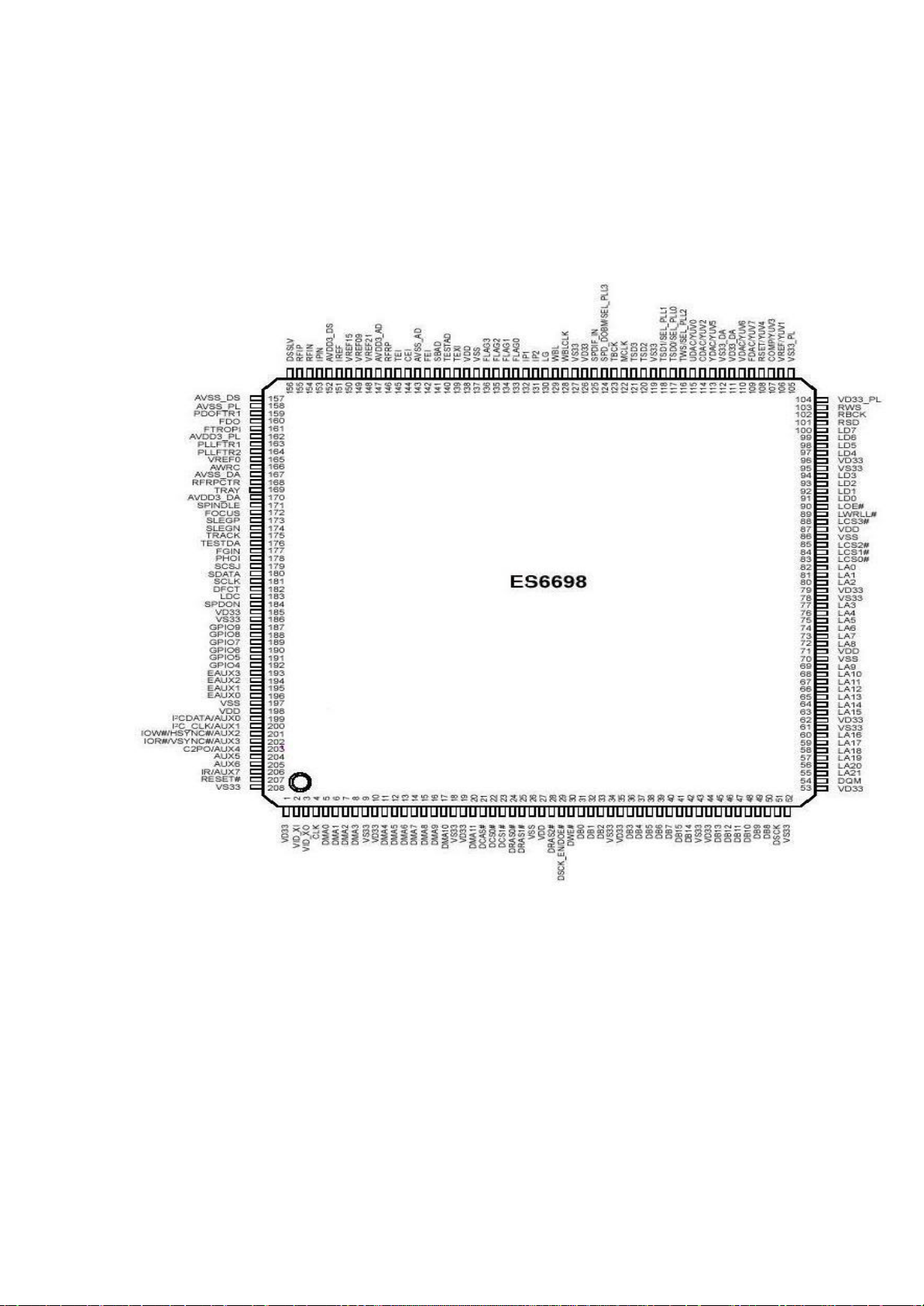
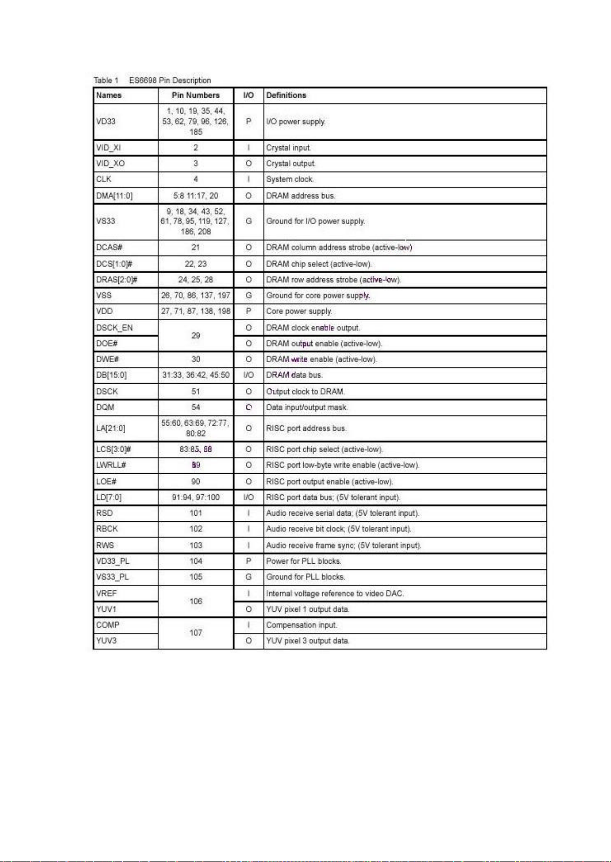
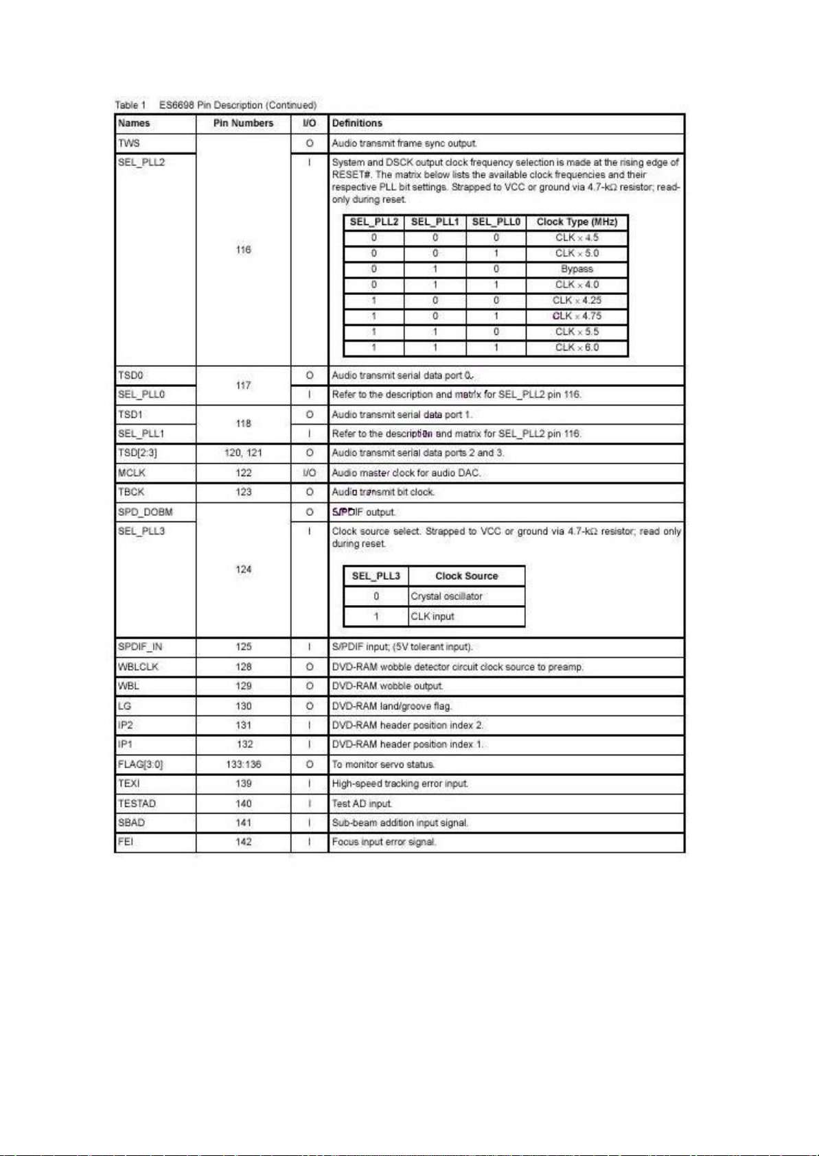
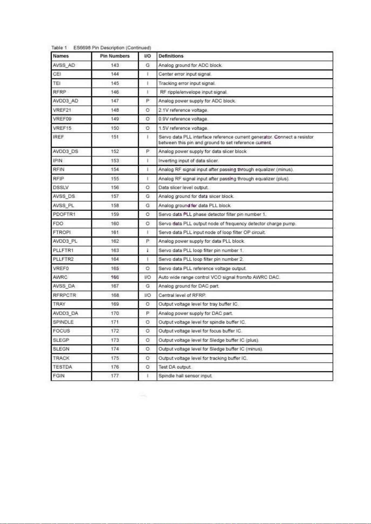
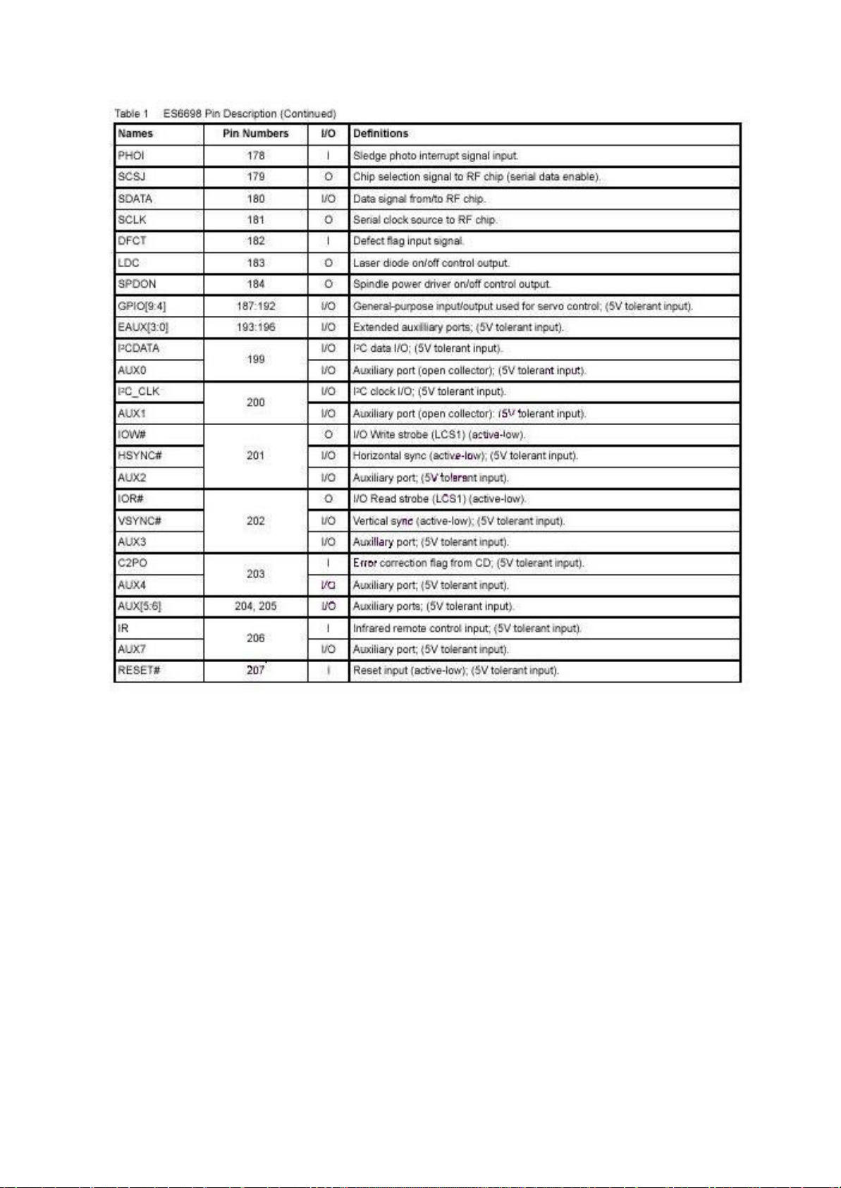
2. System Block Diagram and ES66x8 Pin Description
2.1 ES66x8 Pin Description
4
Page 5
5
Page 6

6
Page 7
7
Page 8
8
Page 9
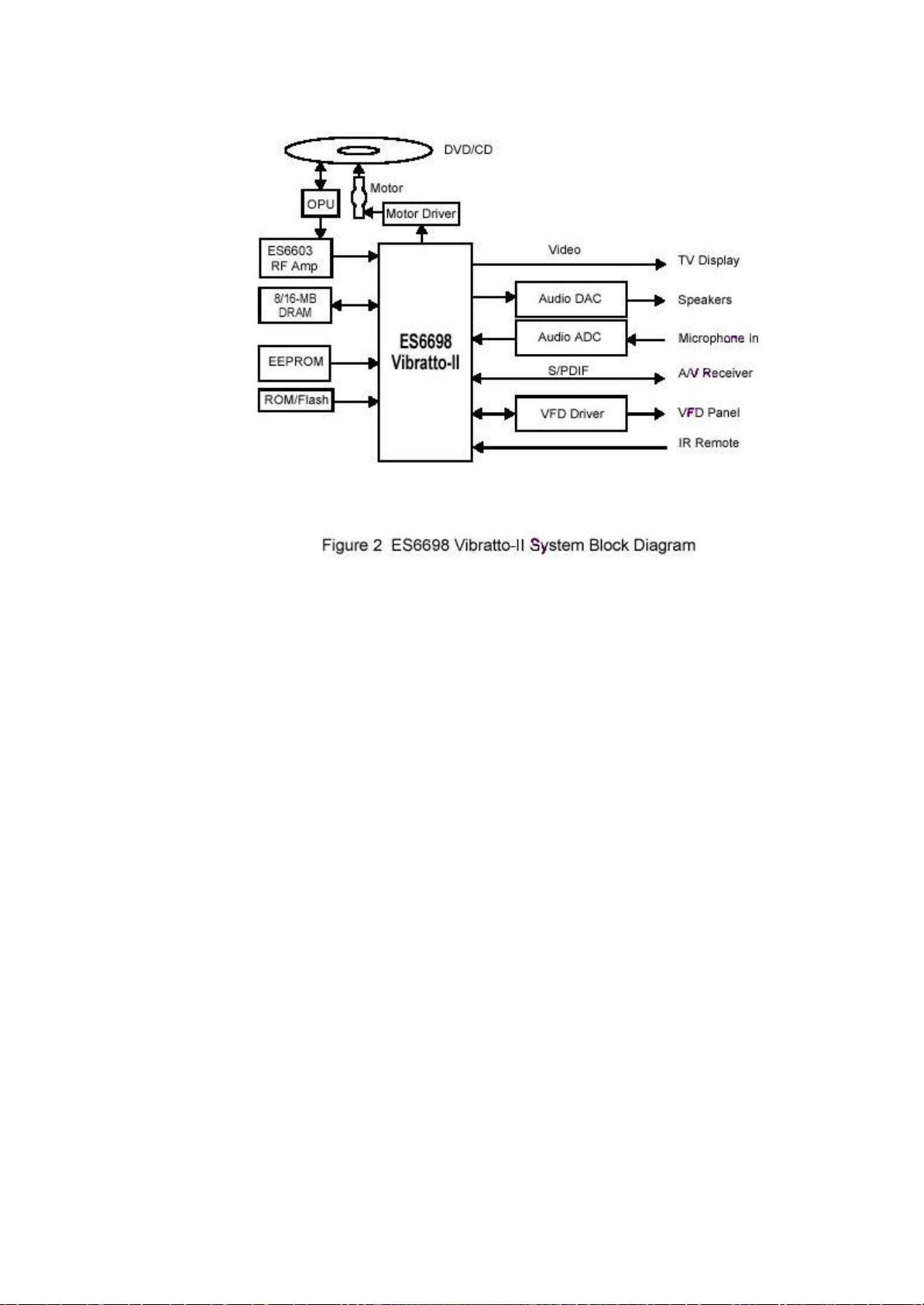
2.1 SYSTEM BLOCK DIAGRAM
A sample system block diagram for the ES66x8 Vibratto II DVD player board design is shown in the
following figure:
9
Page 10
3. AUDIO OUTPUT
The ES66x8 supports two -channel analog audio output while ES66x8 supports six-channel analog audio output.
In a system configuration with six analog outputs, the front left and right channels can be configured to provide
the stereo (2 channel) outputs and Dolby Surround, or the left and right front channels for a 5.1 channel surround
system.
The ES6008 also provides digital output in S/PDIF format. The board supports both optical and coaxial S/PDIF
outputs.
3. AUDIO DACS
The ES66x8 supports several variations of an I2S type bus, varying the order of the data bits (leading or no
leading zero bit, left or right alignment within frame, and MSB or LSB first) is possible using the ES66x8
internal configuration registers. The I2S format uses four stereo data lines and three clock lines. The I2S data and
clock lines can be connected directly to one or more audio DAC to generate analog audio output.
The two-channel DAC is an CS4392. The DACs support up to 192kHz sampling rate.
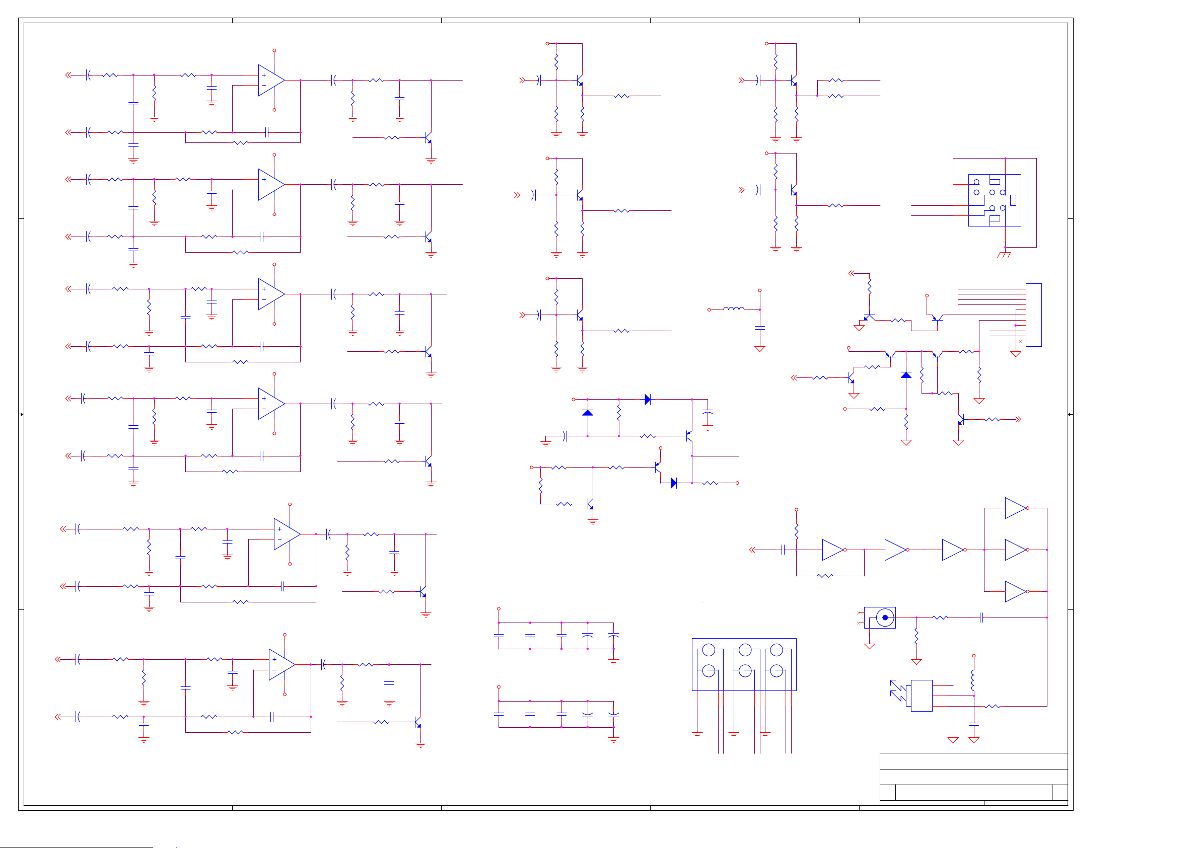
The outputs of the DACs are differential, not single ended so a buffering circuit is required. The buffer circuits
use National LM833 op-amps to perform the low-pass filtering and the buffering.
5 VIDEO INTERFACE
5.1 Video Display Output
The video output section controls the transfer of video frames stored in memory to the internal TV encoder of the
Vibratto II. The output section consists of a programmable CRT controller capable of operating either in Master
or Slave mode.
10
Page 11
The video output section features internal line buffers which allow the outgoing luminance and chrominance data
to match the internal clock rates with external pixel clock rates, easily facilitating YUV4:2:2 to YUV4:2:0
component and sample conversion. A polyphase filter achieves arbitrary horizontal decimation and interpolation.
Video Bus
The video bus has 8 YUV data pins that transfer luminance and chrominance (YUV) pixels in CCIR1656 pixel
format (4:2:2). In this format, there are half as many chrominance (U or V) pixels per line as luminance (Y)
pixels; there are as many chrominance lines as luminance.
Video Post -Processing
The Vibratto II video post-processing circuitry provides support for the color conversion, scaling, and filtering
functions through a combination of special hardware and software. Horizontal up-sampling and filt ering is done
with a programmable, 7-tap polyphase filter bank for accurate
non-integer interpolations. Vertical scaling is achieved by repeating and dropping lines in accordance with the
applicable scaling ratio.
Video Timing
The video bus can be clocked either by double pixel clock and clock qualifier or by a single pixel clock. The
double clock typically is used for TV displays, the single for computer displays.
6 SDRAM MEMORY
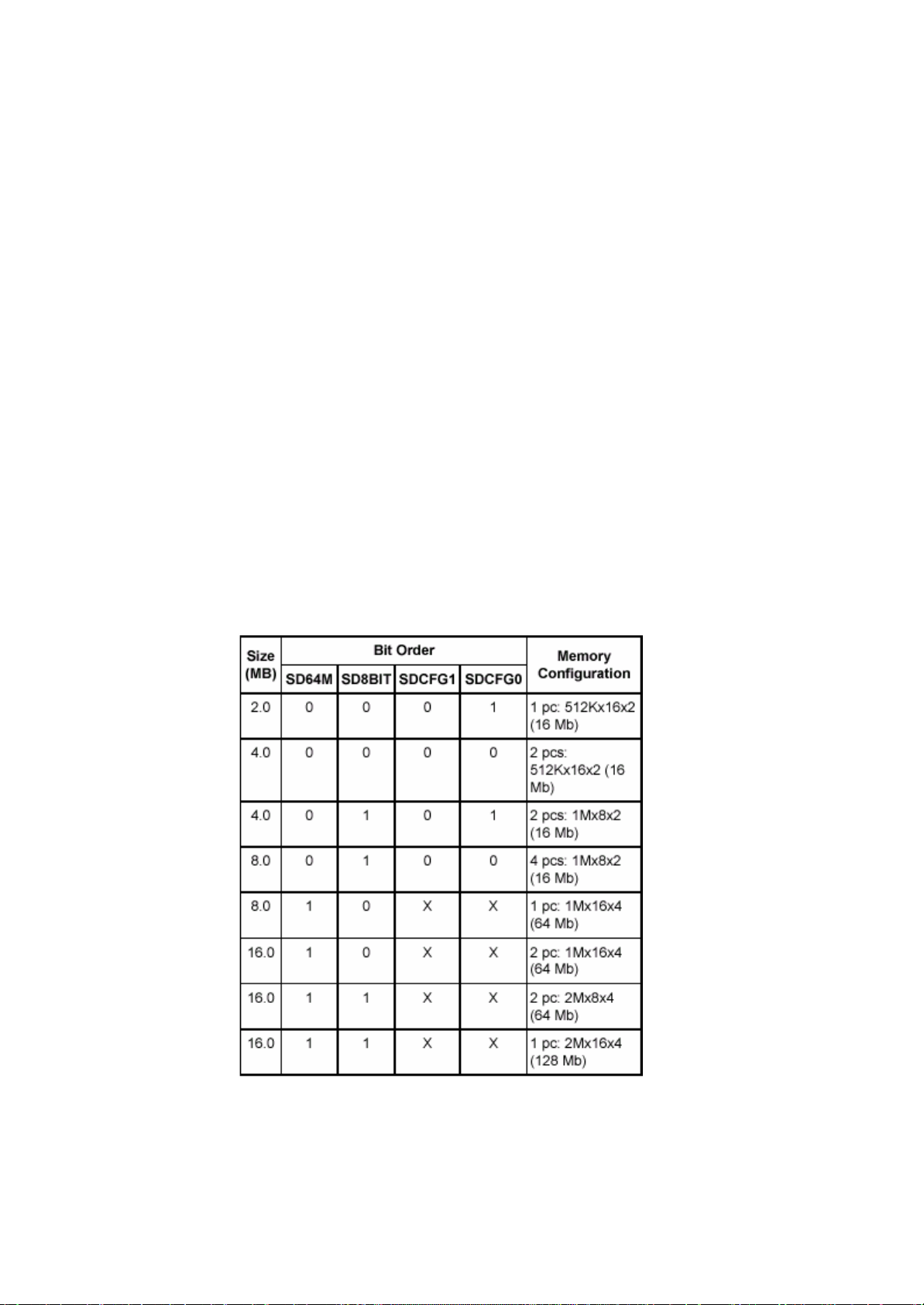
The memory bus interface generates all the control signals to interface with external memory. The Vibratto II
supports different configurations using the memory configuration bits SDCFG[1:0] (bits 12:11), the SD8BIT bit
(bit 14), and SD64M bit (bit 15) in the BUSCON_DRAM_CONTROL register. Configurations can be
implemented in many ways. The following table lists the typical SDRAM configurations used by the Vibratto II.
Typical SDRAM Configurations:
The memory interface controls access to both external SDRAM or EDO memories, which can be the sole unified
external read/write memory acting as program and data memory as well as various decoding and display buffers.
At high clock speeds, the Vibratto II memory bus interface
11
Page 12

has sufficient bandwidth to support the decoding and displaying of CCIR1656/601 resolution images at full
frame rate.
7 FLASH MEMORY
The decoder board supports AMD class Flash memories. Currently 4 configurations are supported:
FLASH_512K_8b
FLASH_1024K_8b
FLASH_512Kx2_8b
FLASH_512Kx2_16b
The Vibratto II permits both 8- and 16-bit common memory I/O accesses with a removable storage card via the
host interface.
8 SERIAL EEPROM MEMORY
An I2C serial EEPROM is used to store user configuration (i.e. language preferences, speaker setup,
etc.) and software configuration.. Industry standard EEPROM range in size from 1kbit to 256kbit and share the
same IC footprint and pinout. The default device is 2kbit, 256kx 8, SOIC8 SGS Thomson ST24C02M1 or
equivalent.
9 AUDIO INTERFACE AUDIO SAMPLING RATE AND PLL COMPONENT
CONFIGURATION
The ES66x8 Vibratto II audio mode configuration is selectable, allowing it to interface directly with
low-cost audio DACs and ADCs. The audio port provides a standard I2S interface input and output and S/PDIF
(IEC958) audio output. Stereo mode is in I2S format while six channels Dolby Digital (5.1 channel) audio output
can be channeled through the S/PDIF. The S/PDIF interface consists of a bi-phase mark encoder, which has low
skew. The transmit I2S interface supports the 128, 192, 256, 384, and 512 sampling frequency formats, where
sampling frequency Fs is usually 32 kHz, 44.1 kHz, 48 kHz, 96 kHz, or 192 kHz. The audio samples for the I2S
transmit interface can be 16, 18, 20, 24, and 32-bit samples.
For Linear PCM audio stream format, the Vibratto II supports 48 kHz and 96 kHz. Dolby Digital audio
only supports 48 kHz. The ES6008/18 Vibratto II incorporates a built-in programmable analog PLL in the device
architecture in order to generate a master audio clock. The MCLK pin is for the audio DAC clock and can either
be an output from or an input to the ES66x8 Vibratto II . Audio data out (TSD) and audio frame sync (TWS) are
clocked out of the Vibratto II based on the audio transmit bit clock (TBCK). Audio receive bit clock (RBCK) is
used to clock in audio data in (RSD) and audio receive frame sync (RWS).
10 FRONT PANEL
10.1 VFD CONTROLLER
The VFD controller is a PTC PT6311. This controller is not a processor, but does include a simple state
machine which scans the VFD and reads the front panel button matrix. The 6311 also includes RAM so it can
store the current state of all the VFD icons and segments. Therefore, the 6311 need only be accessed when the
VFD status changes and when the button status is read. The E S66x8 can control this chip directly using PIO pins
or can allow the front panel PIC to control the VFD.
11 MISCELLANEOUS FUNCTIONS
11.1 RESET CIRCUITRY
Two different chips are supported to provide the power-on-reset and pushbutton reset function:
AAT3521 or V6300.
12
Page 13

12 CONNECTORS
12.1 SCART CONNECTORS
Pinout of the scart connector:
1 ? Audio Right Out
2 ? Audio Right In
3 ? Audio Left / Monu Out
4 ? Audio Gnd
5 ? Blue Gnd
6 ? Audio Left / Mono In
7 ? Blue
8 ? Control Voltage
9 ? Green Gnd
10 ? Comms Data 2
11 ? Green
12 ? Comms Data 1
13 ? Red Gnd
14 ? Comms Data Gnd
15 ? Red
16 ? Fast Blanking
17 ? Video Gnd
18 ? Fast Blanking Gnd
19 ? Composite Video In
20 ? Composite Video Out
21 ? Shield
Some cheaper SCART cables use unshielded wires, which is just about acceptable for short cable lengths. For
longer lengths, shielded coax cable become essential.
Scart Signals:
Audio signals
0.5V RMS, <1K output impedance, >10K input impedance.
Red, Green, Blue
0.7Vpp ?2dB, 75R input and output impedance. Note that the Red connection (pin 20) can alternatively carry the
S-VHS Chrominance signal, which is 0.3V.
Composite Video / CSync
1Vpp including sync, ?2dB, 75R in put and output impedance.Bandwidth = 25Hz to 4.8MHz for normal TV
Video de-emphasis to CCIR 405.1 (625-line TV)
Fast Blanking
75R input and output impedance. This control voltage allows devices to over -ride the composite video input with
RGB inputs, for example when inserting closed caption text. It is called fast because this can be done at the same
speeds as other video signals, which is why it requires the same 75R impedances.
13
Page 14

0 to 0.4V: TV is driven by the composite video input signal (pin 19).
Left unconnected, it is pulled to 0V by its 75R termination.
1V to 3V: the TV is driven by the signals Red, Green, Blue and composite sync. The latter is sent to the
TV on pin 19. This signal is useful when using a TV to display the RGB output of devices such a s home
computers with TV-compatible frame rates. Tying the signal to 5V via 100R forms a potential divider
with the 75R termination, holding the signal at around 2V. Alternatively, if a TTL level (0 to 5V)
negative sync pulse is available, this will be high during the display periods, so this can drive the
blanking signal via a suitable resistor.
Control Voltage
0 to 2V = TV, Normal.
5 to 8V = TV wide screen
9.5 to 12V = AV mode
13. CIRCUIT DESCRIPTION
13.1 POWER SUPPLY:
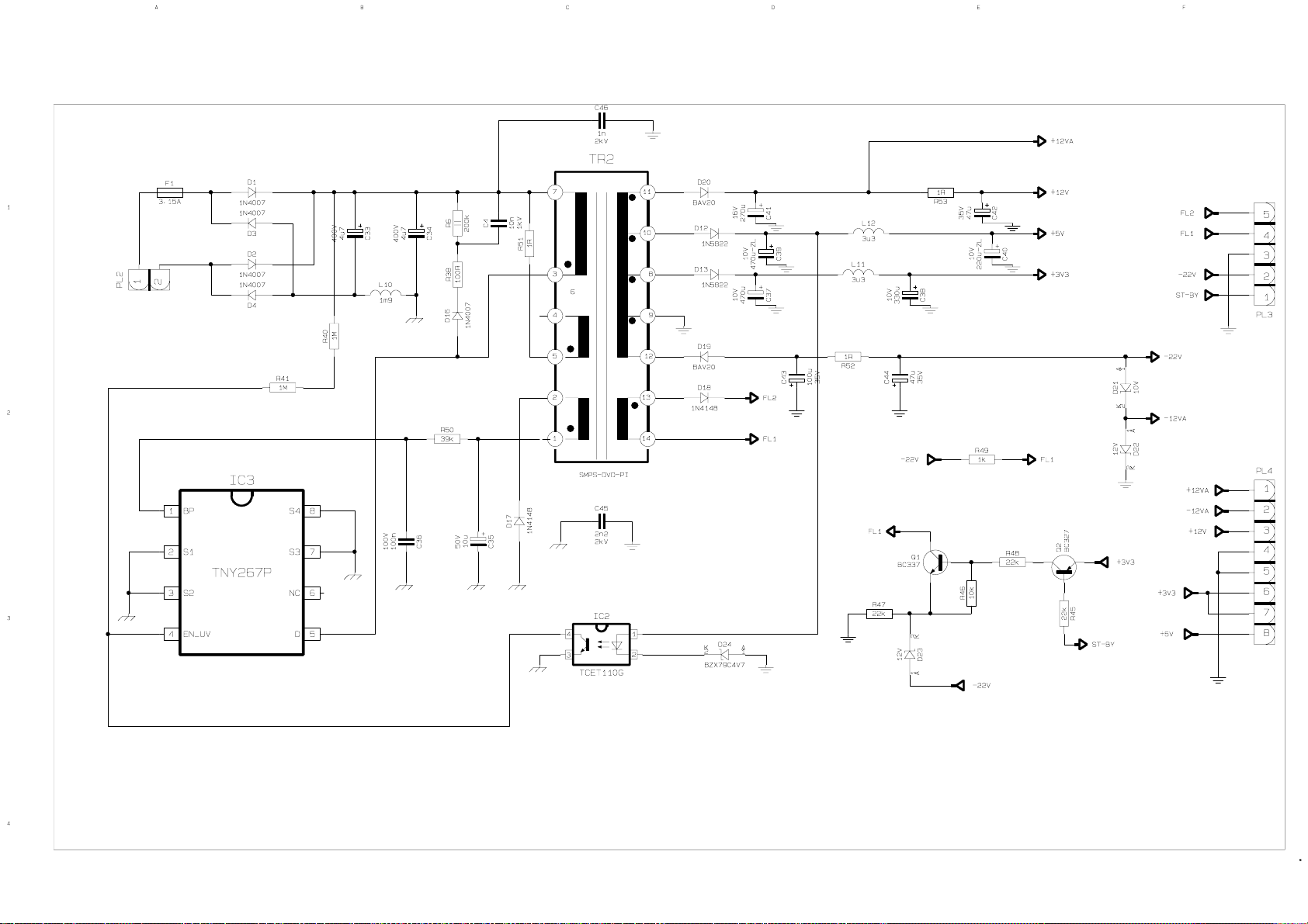
− Socket PL2 is the 220VAC input.
− Socket PL3 is used for the power button on the front panel.
− 3.15A fuse F1 is used to protect the device against short circuit.
− Voltage is rectified by using diodes D1, D2, D3 and D4. Using capacitor C33 (47?f) a DC voltage is
produced. (310 - 320VDC).
− The current in the primary side of the transformer TR2 comes to the SMPS IC (TNY267P). It has a built-in
oscillator, over current and thermal protection circuitry and runs at 133 kHz. It starts with the current from
the primary side of the transformer and follows the current from the feedback winding.
− Voltages on the secondary side are as follows: 12 Volts at pin11 at C42, 5 Volts at C40,3.3 Volts at C38,
-22Volts at C44, -12 Volts at D22.
− D14 TL431 is a constant current regulator. TL431 watches the 5 volts and supplies the required current to
IC2. There are a LED and a photo transistor in IC2. The LED inside the IC2 transmits the value of the
current from D25 to phototransistor. Depending on the current gain of the phototransistor IC3 keeps the
voltage on the 5-volt-winding constant.
− –22 Volts is used to feed the VFD (Vacuum Fluorescent Display) driver IC on the front panel.
14
Page 15

Functional Block Diagram of Switcher
13.2 FRONT PANEL:
− All the functions on the front panel are controlled by U1 (ES66x8) on the mainboard.
− U1 sends the commands to IC2 PT6311 via socket J2 (pins 3,4 and 5).
− There are 48 keys scanning function, 5 LED outputs, 1 Stand-by output and VFD drivers on PT6311.
− Vacuum fluorescent display is specially designed for DVD.
− The scanned keys are transmitted via PT6311 to U1 on the mainboard.
− IR remote control receiver module sends the commands from the remote control directly to U1.
13.3 BACK PANEL:
− There are 1 SCART connector (con24), 2 pieces RCA audio jacks for audio output, 1 coaxial digital audio
output and 1 laser digital audio output on the back panel.
− MOFT3C2 is used for laser output.
− Left and right audio outputs are on RCA Conn 6.
− LUMA and CHROMA signals of S-Video are transmitted to P1 via transistors Q39 and Q37 respectively.
15
Page 16

CD Update Procedure of 4250D
1. Download the update file from the convenient link according to your default language choice.
2. While there is no CD in the DVD (No Disc Mode) , press “Menu 1 3 5 7” buttons on the remote control
in order to reach the Servi ce Menu of DVD Player:
2.1. Note the software version described as “b.xx “ to be able to compare the sw. Version after update
process.
3. Copy the update file to the desktop and rename it according to the update file name in the hidden menu of
the device.
For example If C2M1AS__ is written then rename it like C2M1AS__.rom
If P6M1AS__ is written then rename it like P6M1AS__.rom
(If you receive the update file already renamed (with addition of .rom) from the customer technical support
department by giving the SAP code of the product then burn the already renamed file with nero program as
it is shown below.)
4. Burn the renamed files by Nero program with below set up.
5. After burning process is completed, place the update CD into the DVD tray and press play button.
6. Wait to see the update process steps as shown below. When the sw. Update is completed unit will switch
itself to standby mode.
7. Finally, press the eject button and take out the update CD while DVD Player remains at stand by Mode.
8. Updating process has been completed. To check whether it is updated correctly or not, repeat the first step
for comparing software version
9. If the previous and letter names are different, CD is update has completed successfully. If the name remains
same than go through the steps from the beginning.
IMPORTANT NOTE: If the AC source breaks down while the updating the unit (main board) will be
totally out of order. This kind of units/boards is out of Warranty.
16
Page 17
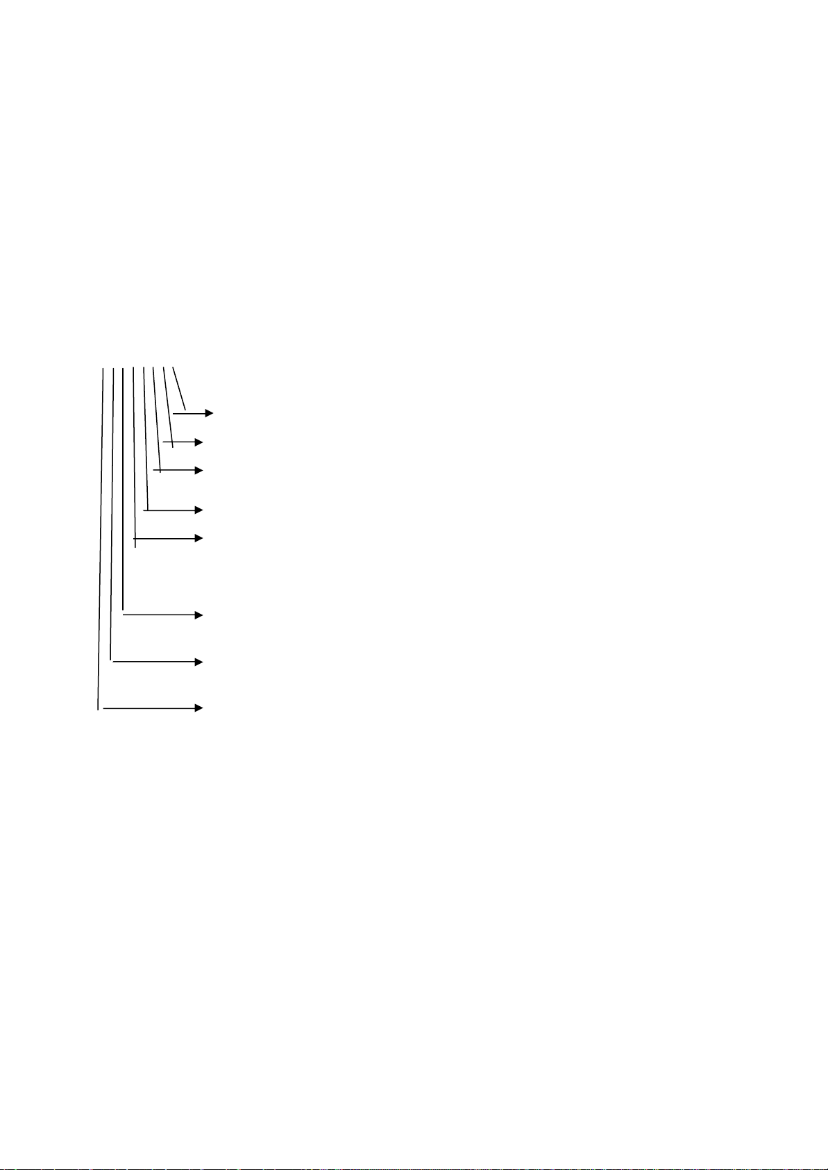
Brief Information of Naming the File
Software version differs from each other depending on front models. 23xx and 24xx are called Old VFD and
25xx and 26xx are called Mini VFD. Each character in the file name is an abbreviation of a description as
illustrated below.
C2M1AS__
Progressive Option (with progressive : P, without progressive: _ )
DMR option (with DMR:R, without DMR:_ )
Loader Type (S loader:s W loader:w)
Flash Type ( AMD:A, Intel:I )
Language group
VFD type
DAC channel (2, 6)
DAC Type
17
Page 18
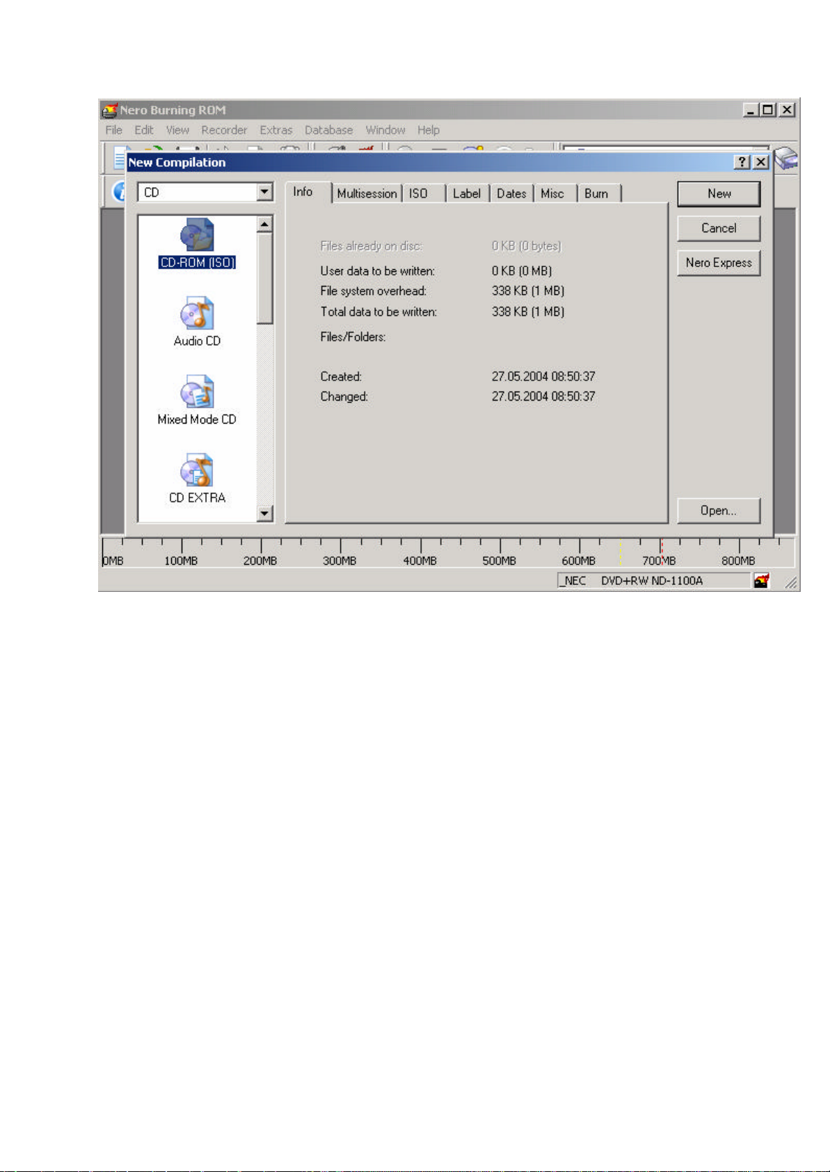
Pay attention the left side. Select CD and CD_ROM (ISO) on the upper left side of screen
18
Page 19
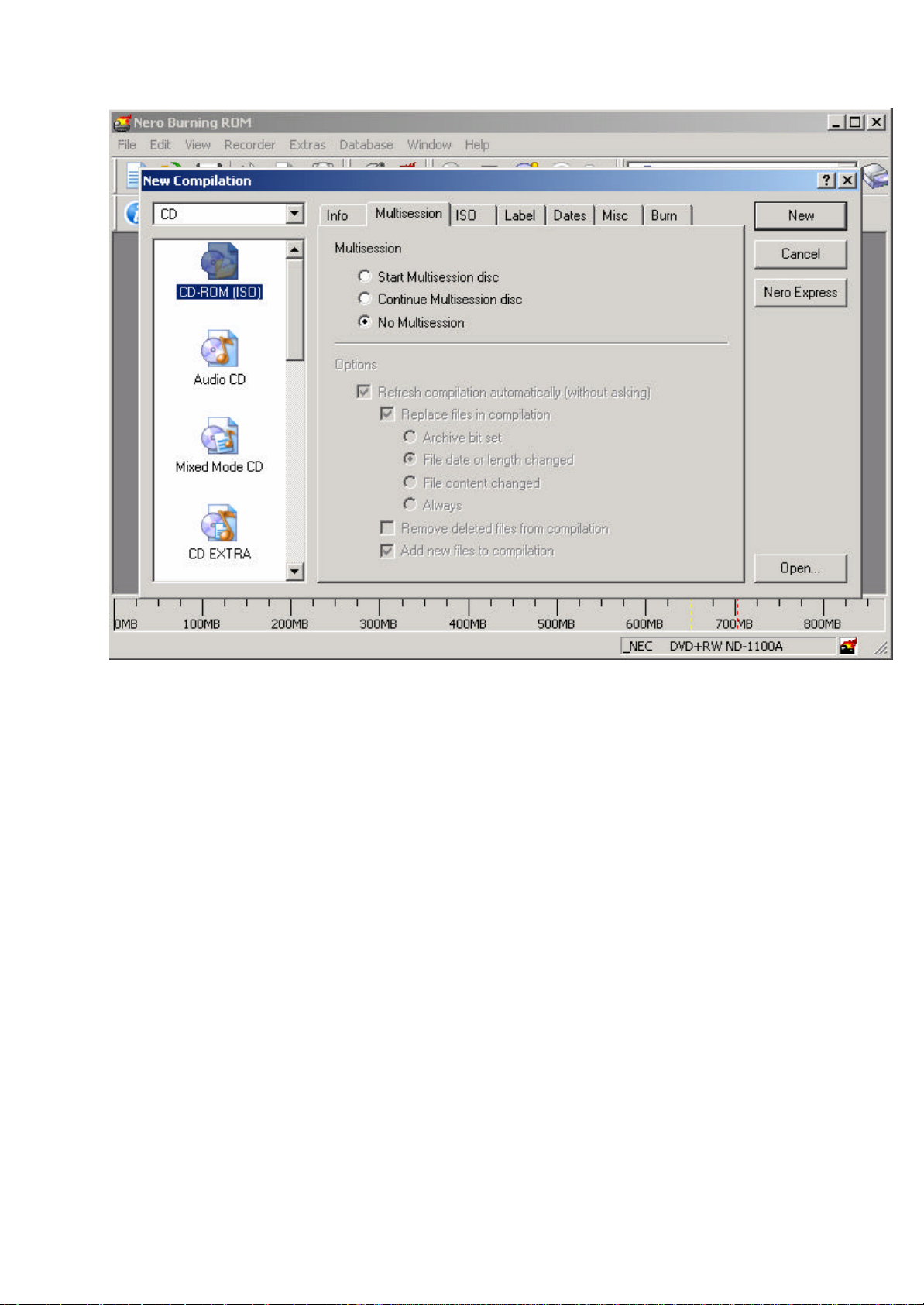
Select No Multisession
19
Page 20
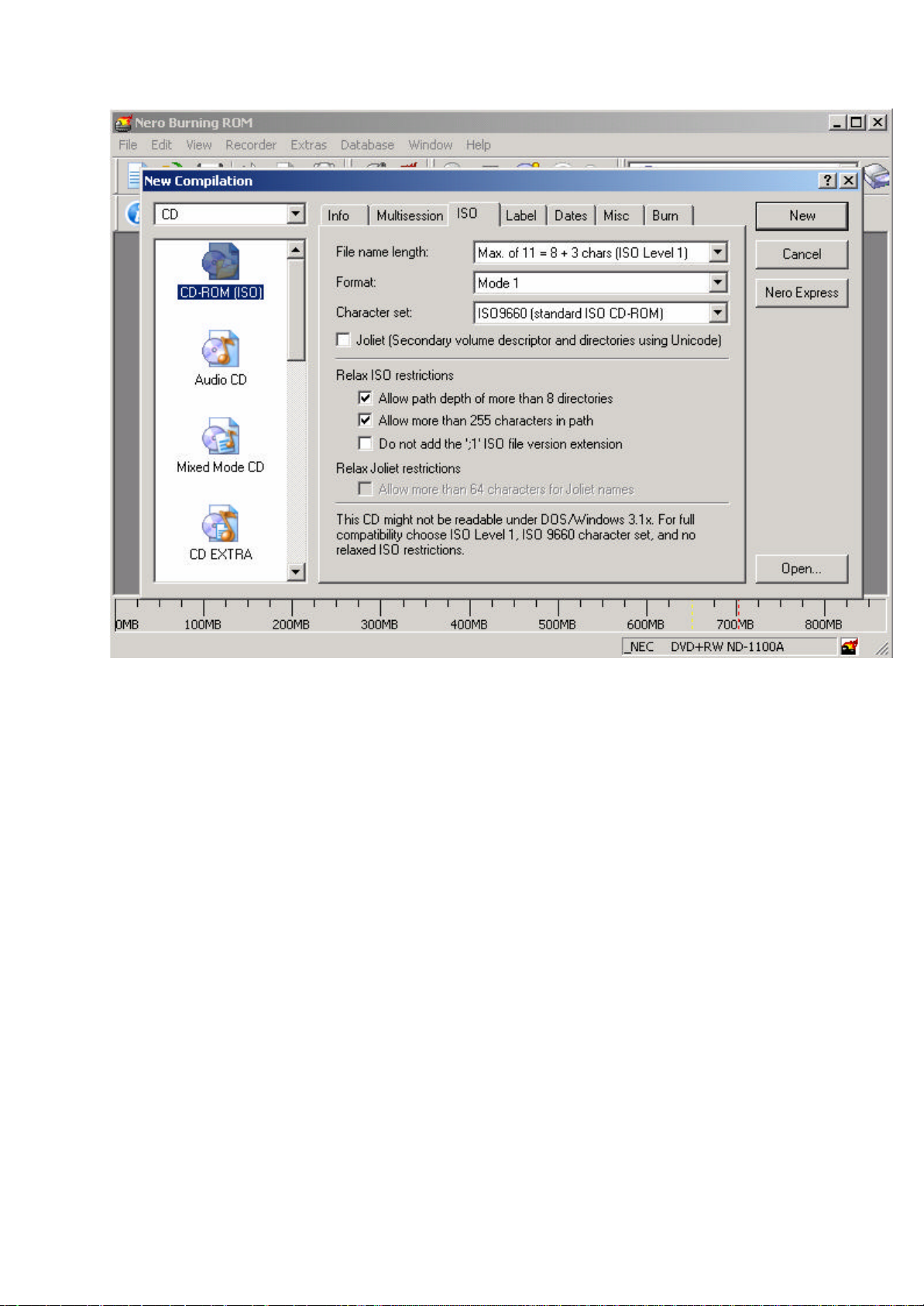
Format is Mode 1
20
Page 21
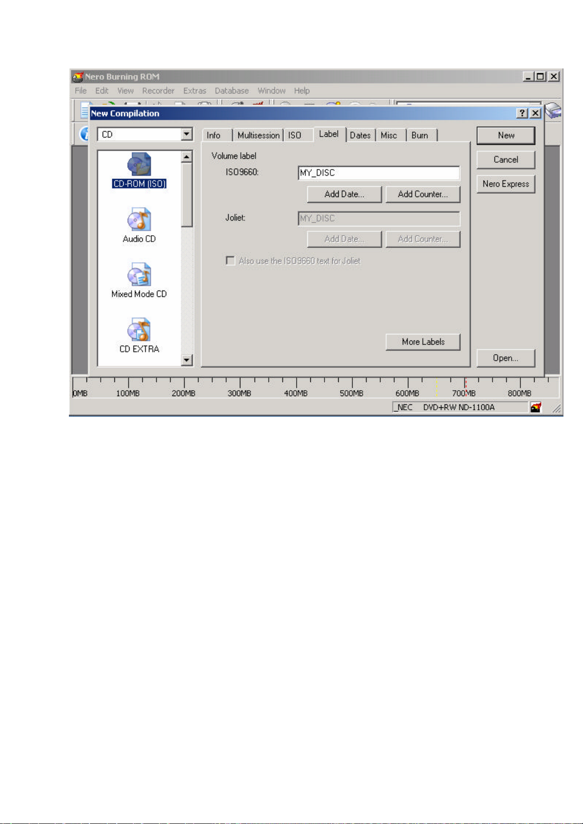
21
Page 22
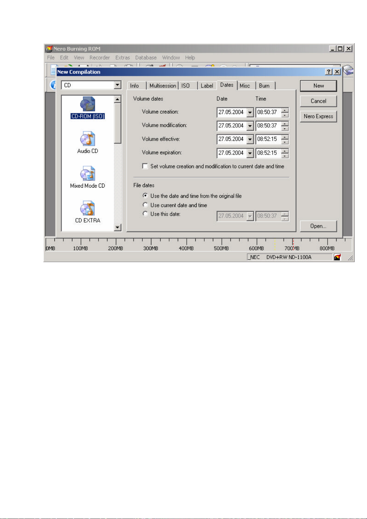
Leave the dates as it is
22
Page 23
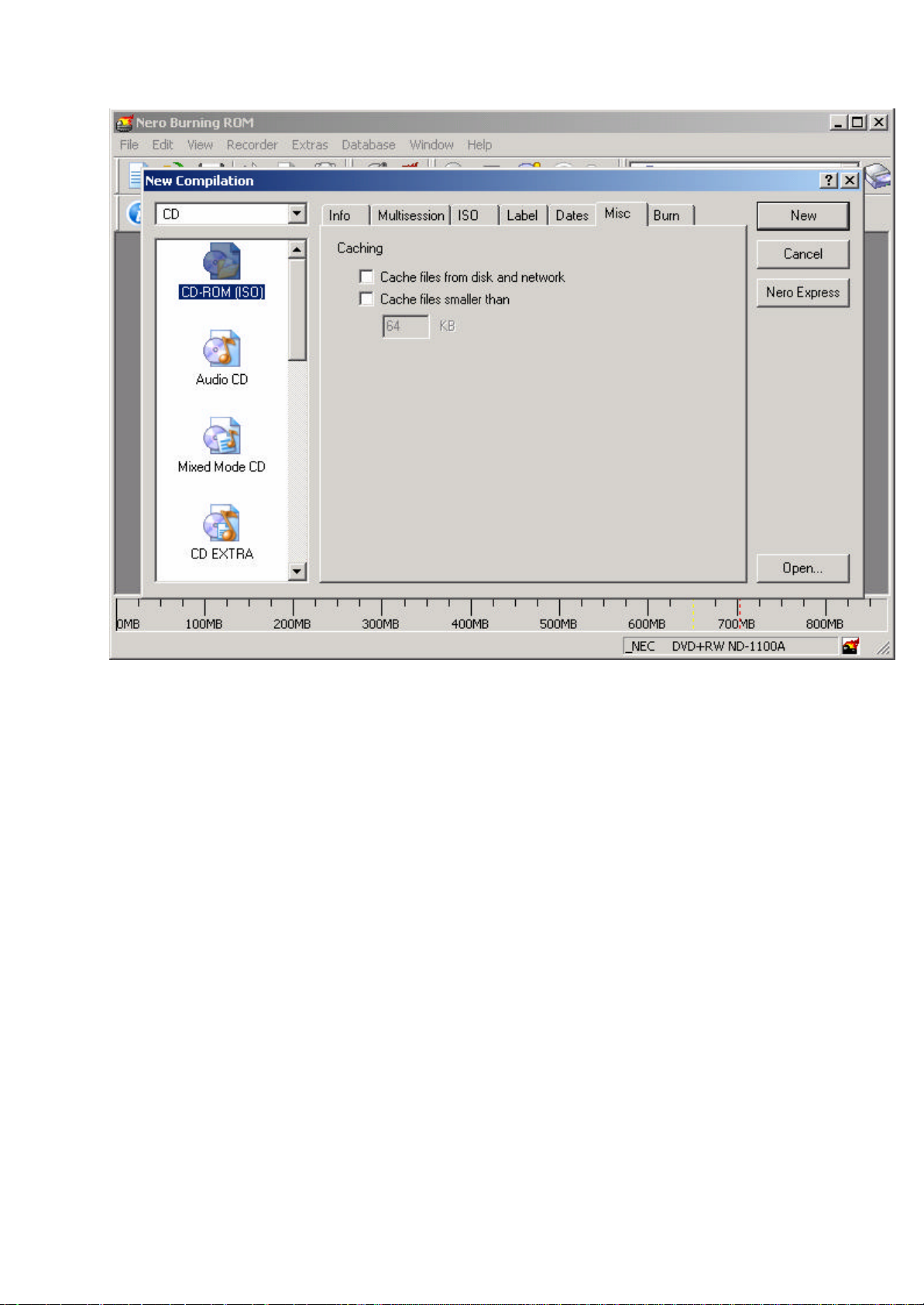
Leave it as it is
23
Page 24
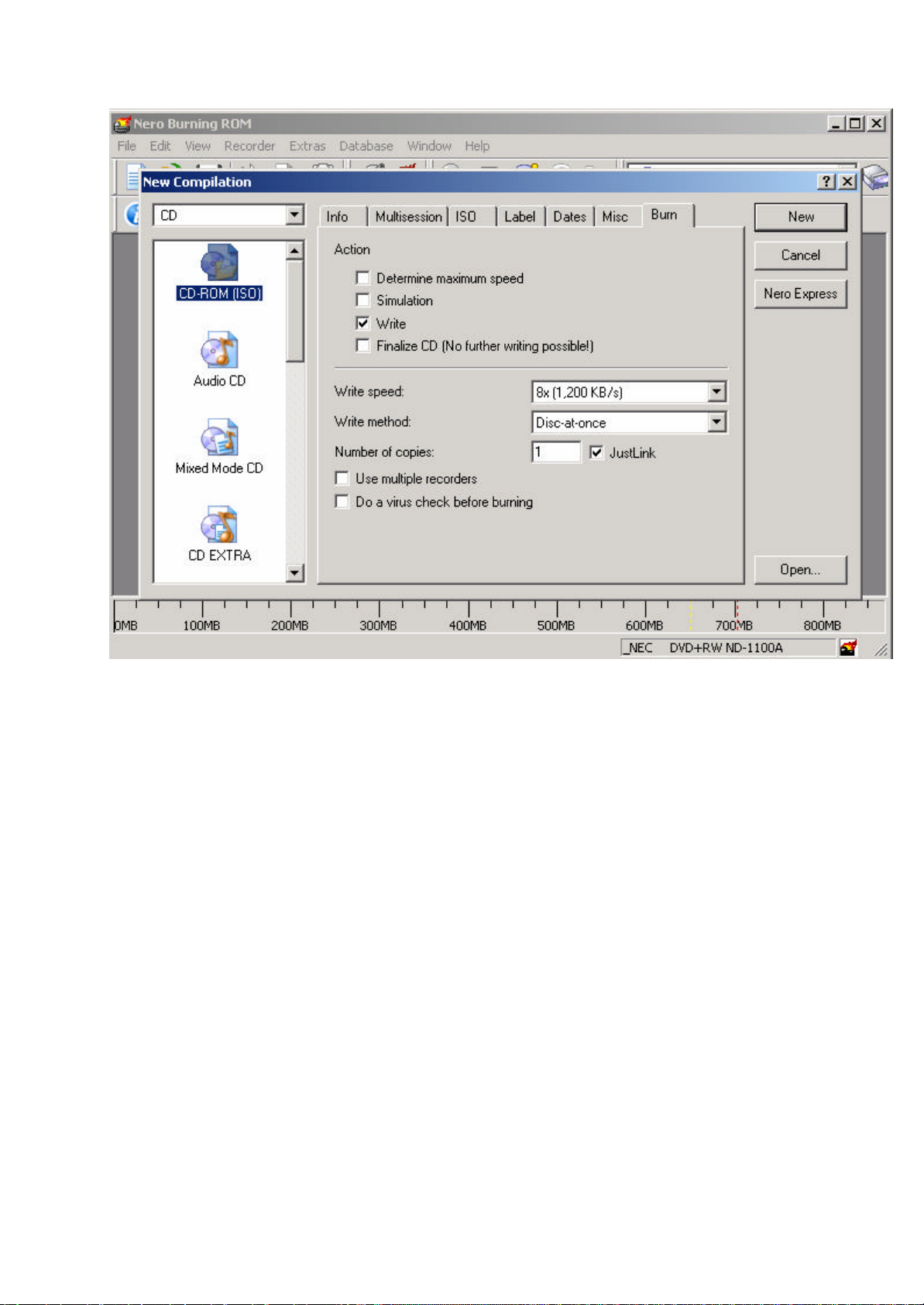
Click the “New” on the upper right corner of the screen
24
Page 25
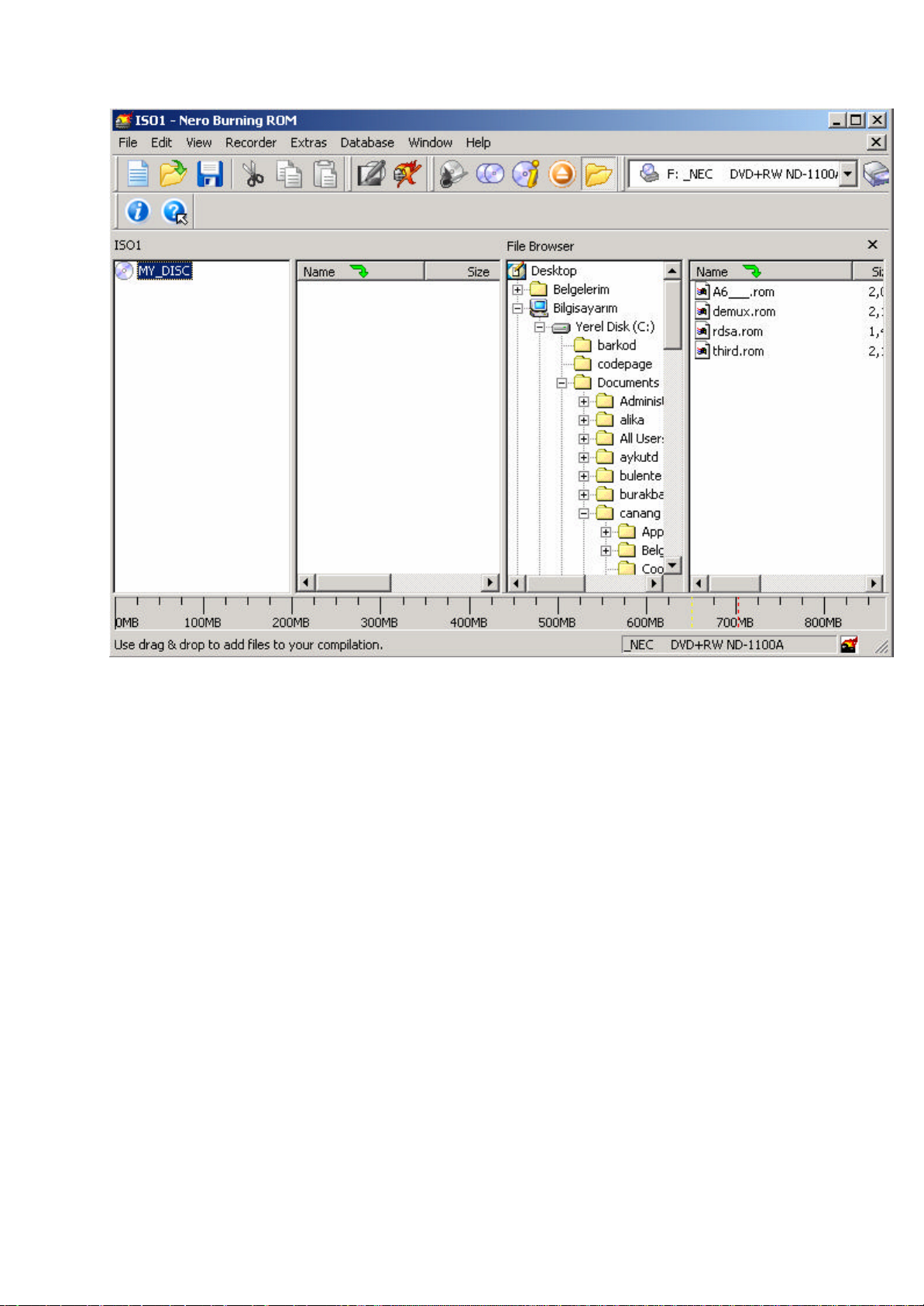
Select your file from file browser then you will see your file in the “Name” section on the right side and then
copy the files to under “Name” section on the left side.(this is just an example you will see your file name when
you are doing this process)
25
Page 26

Click the “Burns the current compilation”
26
Page 27
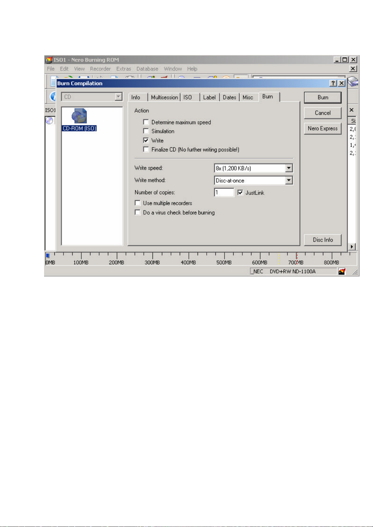
Then you will see this screen and click the “Burn” on the right upper side of screen
27
Page 28
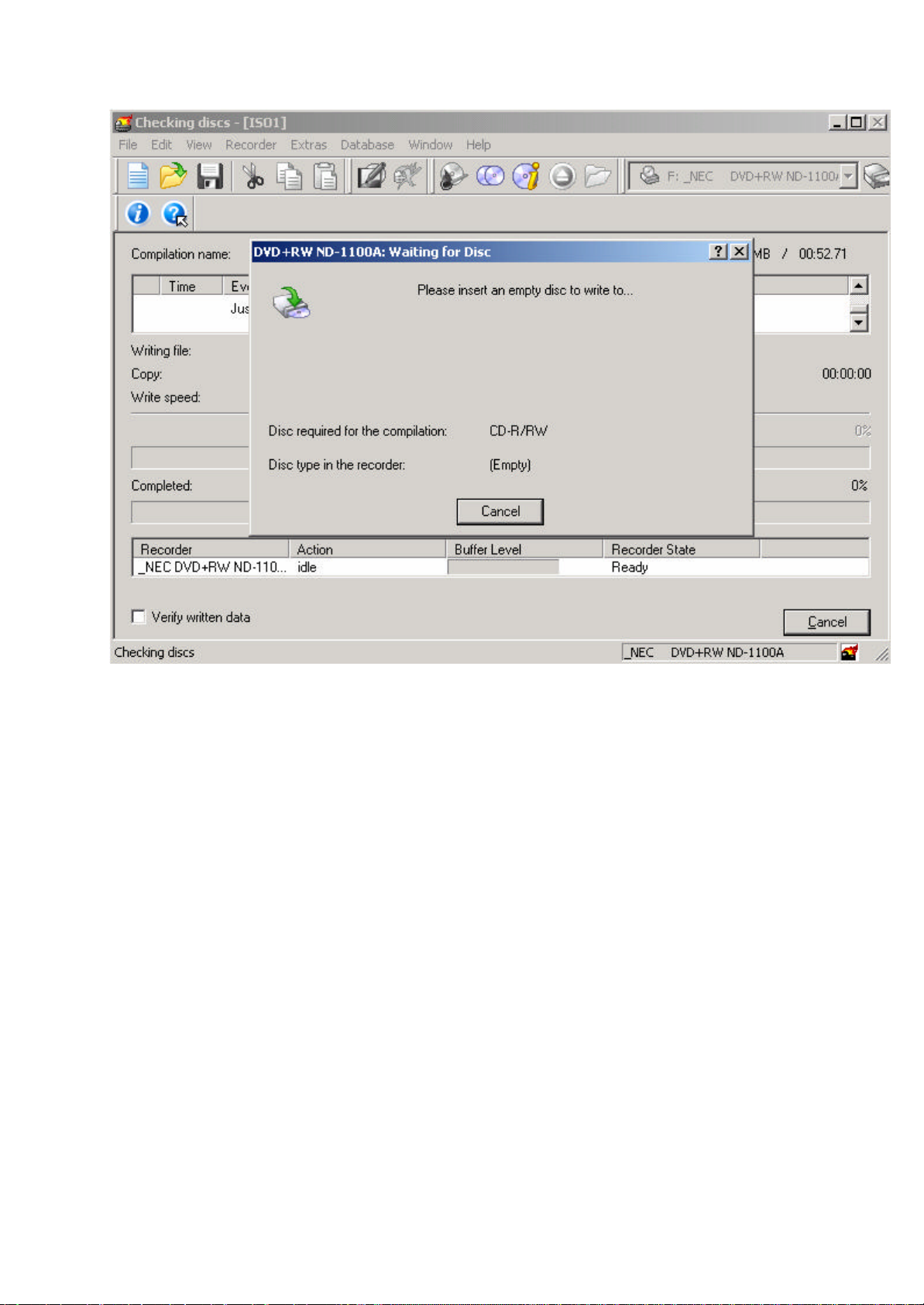
You will see this screen and tray will open itself on computer ,then place the CD in CD-ROM
And it will start writing. At the end you will see “burn complited”
.
28
Page 29

MOCTL(3)
SVREF21(3)
VCC33
MIRR(3)
ATR_OP(3)
SERIAL EEPROM
1
2
3
4 5
GND
MA0
MA1
MA2
MA3
MA4
MA5
MA6
MA7
MA8
MA9
MA10
MA11
DSCK
DOE#
CS0#
RAS0#
CAS#
DWE#
DQM
RAS1#
RAS2#
XFLAG0
XFLAG1
XFLAG2
XFLAG3
RFO
TESTAD
DA
RFRP
DIP
DIN
TRACK
FOCUS
SLEGP
SLEGN
SPINDLE
MIRR
TEI
FEI
CEI
SPDON
SFGIN
R51 0
SVREF21
DEFCT
SPDON
SLDC
RR12 R
CC28 0.015U7.5nF
VCC
S0
S1
WC
S2
SCL
GND SDA
24C01A
R33 33
R69 33
R58 33
R57 33
R40 33
R41 33
R44 33
R46 33
R47 33
TP1
FLAG0
TP3
FLAG2
TP5
RFO
TP7
DA
TP9
DIP
TP11
STRACK
TP13
SSLEGP
TP15
SSPINDLE
TP17
TEI
TP19
CEI
TP21
FGIN
10x4
RN4
RR10 0
RR15 33K
OPEN(3)
SPINDLE(3)
FOCUS(3)
SLEGN(3)
TRACK(3)
AM5868 BA5954
SVREF15(3)
SCSJ(3)
SDATA(3)
SCLK(3)
VCC
U3
8
7
6
GND
TP2
FLAG1
TP4
FLAG3
TP6
TESTAD
TP8
RFRP
TP10
DIN
TP12
SFOCUS
TP14
SSLEGN
TP16
MIRR
TP18
FEI
TP20
XSPDON
RS232_DET
SDEFCT (3)
SPDON (3)
SLDC (3)
EAUX40
18
EAUX41
27
EAUX42
36
EAUX43
45
RFRP
RR87 0
SPINDLE
FOCUS
SLEGN
TRACK
SVREF15
SCSJ
SDATA
SCLK
R52
1K
NN(5)
SCART-ON(5)
U5
23
A0
24
A1
25
A2
26
A3
29
A4
30
A5
31
A6
32
A7
33
A8
34
A9
22
A10
35
A11
38
CLK
37
CKE
19
CS
18
RAS
17
CAS
16
WE
15
DQML
39
DQMH
20
BA0
21
BA1
36
NC
40
NC
4Mx16 SDRAM (9ns)
32/64MBIT SDRAM
TESTAD
SVREF15
CC20
1U
PLLGNDRFGND
CC28
0.015U
R53
1K
RFGND
R23 33
R65 33
R64 33
R26 33
DQ10
DQ11
DQ12
DQ13
DQ14
DQ15
VCCQ
VCCQ
VCCQ
VCCQ
VSSQ
VSSQ
VSSQ
VSSQ
CC35
33P
DQ0
DQ1
DQ2
DQ3
DQ4
DQ5
DQ6
DQ7
DQ8
DQ9
VCC
VCC
VCC
VSS
VSS
VSS
CC32
0.015U
CC36
33P
2
4
5
7
8
10
11
13
42
44
45
47
48
50
51
53
1
14
27
3
9
43
49
6
12
46
52
28
41
54
TR1
TR2
CC24
0.1U
SVREF15
CC33
560P
CC37
33P
VCC33
GND
RR1 4.7K
VCC33
RR2 4.7K
TXD
RS232_DET
RXD
RS232 CONNECTOR 2.54MM
RF33V
RR14 R
RR16 1.2K
RR17 10K
RR18 5.1K
CC26
0.1U
DA
CC31
0.015U
VCC
IR
VFD-CLK
VFD-CS
VFD-DATA
CC25
47P
CC30
560P
DB0
DB1
DB2
DB3
DB4
DB5
DB6
DB7
DB8
DB9
DB10
DB11
DB12
DB13
DB14
DB15
VCC
GND
SBAD(3)
FEI(3)
CEI(3)
TEI(3)
DIP(3)
RFO(3)
DIN(3)
CC13
0.1U
RFGND
CC18
C
CC19
C
CC21
0.047U
CC23
560P
RR96 0
RR21 6.8K
RR22 6.8K
RR24 5.1K
RR25 6.8K
RR26 6.8K
RR27 33
RR28 33
RR29 33
INSW(3)
HOMESW(3)
CLOSE(3)
OUTSW(3)
DRVSB(3)
EAUX43(4)
EAUX42(4)
EAUX41(4)
EAUX40(4)
R31 33
R54 33
R60 4.7K
R55 33
R56 33
JJ1
1
2
3
4
5
SBAD
FEI
CEI
TEI
DIP
RFO
DIN
CC14
CC15
0.1U
0.1U
PLL33V
CC22
0.1U
TR1
TR2
CC27
0.1U
SLEGP
SFGIN
XSCSJ
XSDATA
XSCLK
DEFCT
SLDC
SPDON
RS232_DET
RESET#
R42 100K
Y1
27M
C13
C14
27PF
27PF
GND GNDGND
SERVO MCU
DEBUG
HEADER
RFGND
CC58
4700P
CC59
C
CC61
C
CC55
4700P
RR8 68K
RR9 20K
CC16
C
CC17
6800P
RFGND
157
AVSS_DS
158
AVSS_PL
159
XSPDOFTR1
160
XSFDO
161
XSFTROPI
162
AVDD3_PL
163
XSPLLFTR1
164
XSPLLFTR2
165
XSVREF0
166
XSAWRC
167
AVSS_DA
168
XSRFRPCTR
169
XSTRAY
170
AVDD3_DA
171
XSSPINDLE
172
XSFOCUS
173
XSSLEGP
174
XSSLEGN
175
XSTRACK
176
XSTESTDA
177
XSFGIN
178
XSPHOI
179
SXCSJ
180
XSDATA
181
XSCLK
182
XSDFCT
183
XSLDC
184
XSSPDON
185
VD33
186
VS33
187
XGPIO[9]
188
XGPIO[8]
189
XGPIO[7]
190
XGPIO[6]
191
XGPIO[5]
192
XGPIO[4]
193
EAUX03
194
EAUX02
195
EAUX01
196
EAUX00
197
VSS
198
VDD
199
AUX0
200
AUX1
201
AUX2/ HSYNC
202
AUX3/ VSYNC
203
AUX4
204
AUX5
205
AUX6
206
AUX7
207
RESET
208
VS33
FB4
3.3UH
PLL30CLK SOURCE
1
DCLK INPUT
CRSTAL OSC
CC1
CC2
1000P
CC3
1000P
1000P
CC4
1000P
RR3 3.3K
RR4 3.3K
RR5 3.3K
RR6 3.3K
CC5
0.1U
RR7 10K
CC8 4.7U
154
155
156
XSRFIP
XSDSSLV
152
153
XSIPIN
XSRFIN
CC46
CC12
SVREF15
SVREF09
149
150
151
XSIREF
AVDD3_DS
XSVREF[09]
XSVREF[15]
SVREF21
RFRP
146
147
148
XSRFRP
AVDD3_AD
XSVREF[21]
1U
1U
145
XSTEI
144
XSCEI
143
TESTAD
140
141
142
XSFEI
XSSBAD
AVSS_AD
VCC20
137
138
139
VSS
VDD
XSTEXI
XSTESTAD
XFLAG1
XFLAG3
XFLAG2
134
135
136
XSFLAG[2]
XSFLAG[3]
RXD
XFLAG0
133
XSFLAG[0]
XSFLAG[1]
XS
132
XSIP1
TXD
131
TP36
XS
130
XSLG
XSIP2
TP37
XS
128
129
XSWBL
XSWBLCLK
127
TP38
126
VS33
125
VD33
SPDIF
MCLK
TSD2
TBCK
120
121
122
123
124
TSD3
TBCK
MCLK
SPDIFIN
SPDIF/SEL_PLL3
TSD0
TSD1
TWS
117
118
119
VS33
TSD2
TSD0/SEL_PLL0
TSD1/SEL_PLL1
UDAC1
115
116
YUV0/UDAC
TWS/SEL_PLL2
Vibratto-II
VD33
XIN
XOUT
DCLK
DMA0
DMA1
DMA2
DMA3
VS33
VD33
DMA4
DMA5
DMA6
DMA7
DMA8
DMA9
DMA10
VS33
VD33
DMA11
DCAS
DCS0
DCS1
DRAS0
DBANK0/ DRAS1
VSS
VDD
DBANK1/ DRAS2
DCKE/DOE/TDMTSC
DWE
DB0
DB1
DB2
VS33
VD33
DB3
DB4
DB5
DB6
DB7
DB15
DB14
123456789101112131415161718192021222324252627282930313233343536373839404142434445464748495051
C15
1000PF
R43
0
DMA1
DMA2
DMA0
XOUT
XIN
DCLK
1 8
2 7
MA1
MA0
MA2
3 6
DMA3
4 5
MA3
RN1 10x4
DMA4
1 8
MA4
DMA5
2 7
MA5
DMA6
3 6
MA6
DMA7
4 5
MA7
DMA8
DMA9
RN2 10x4
DMA10
1 8
2 7
MA8
MA9
3 6
MA10
CAS#
DMA11
4 5
MA11
CS0#
10x4
RN3
RAS0#
DOE#
RAS2#
DWE#
RAS1#
U10
RESET
GND
NC
EN
VCC
AAT3521 SOT-23(5pin)
U11
GND
RESET
VCC
AAT3520 SOT-23(3pin)
DB0
1
2
3
4
5
1
2
3
DB1
DB2
DB5
DB4
DB3
VCC
R19 100K
R37
OPEN\0
R36
OPEN\0
GND
DB6
DB7
DB15
DB14
VCC33 VCC33VCC33VCC33
R1
OPEN
R7
4.7K
CDAC1
VCC33V
VDAC1
GNDV
RSET
FDAC1
YDAC1
109
110
111
112
113
114
VS33_DA
VD33_DA
YUV7/FDAC
YUV6/VDAC
YUV5/YDAC
YUV2/CDAC
VS33
VD33
DB13
DB12
DB11
DB10
DB9
DB10
DB12
DB11
DB13
RESET#
EM-MARIN
RESET IC
U10
AAT3521
V6300 OPEN
R2
OPEN
R8
4.7K
COMP
VREF
VS33_PL2
105
106
107
108
YUV1/VREF
YUV4/RSET
YUV3/COMP
RWS/TDMFS
RBCK/TDMCLK
RSD/TDMDR
DB9
DB8
DSCK
52
DSCK
DB8
RESET# (3)
R36
OPEN
0
VS33_PL
VS33
R3
R4
OPEN
OPEN
SPDIF (5)
TBCK (4)
MCLK (4)
TSD2 (4)
TSD1 (4)
TSD0 (4)
TWS (4)
R10
R9
4.7K
4.7K
R59 390
C7 0.1U
R50 0 OHM
U1
ES66x8
104
VD33_PLL
103
102
101
100
LD7
99
LD6
98
LD5
97
LD4
96
VD33
95
VS33
94
LD3
93
LD2
92
LD1
91
LD0
90
LOE
89
LWRLL
88
LCS3
87
VDD
86
VSS
85
LCS2
84
LCS1
83
LCS0
82
LA0
81
LA1
80
LA2
79
VD33
78
VS33
77
LA3
76
LA4
75
LA5
74
LA6
73
LA7
72
LA8
71
VDD
70
VSS
69
LA9
68
LA10
67
LA11
66
LA12
65
LA13
64
LA14
63
LA15
62
VD33
61
VS33
60
LA16
59
LA17
58
LA18
57
LA19
56
LA20
55
LA21
54
DQM
53
VD33
GND
VCC
R37
0
PLL2
0
0 1
0
0
1
1
VCCV VCC
R5
4.7K
GNDGND GNDGND GND
VCC33V
C8 0.1U
GND
VD33_PL1
LD7
LD6
LD5
LD4
LD3
LD2
LD1
LD0
LOE#
WRLL#
LCS3#
LCS2#
LA0
LA1
LA2
LA3
LA4
LA5
LA6
LA7
LA8
LA9
LA10
LA11
LA12
LA13
LA14
LA15
LA16
LA17
LA18
LA19
LA20
LA21
DQM
IR
VCC
VFD-DATA
VFD-CLK
VFD-CS
GND
0
0
1 27bypass
1
0
0
11
1
FB1
FERB
J2
1
2
3
4
5
6
HDR6-100
VCC33
FB2
FERB
VCC20
IR
+5V
VFD-DATA
VFD-CLK
VFD-CS
GND
0
1
1
0
1
GNDV
4.25
reserved 5
bypass
3.75
4.501
reserved
3.5
4
DEFAULT
PLL0
0
MULTI
S-CHIP
DEFAULTPLL1
114.75
4.5
NA
101.25
4
121.5
4.25
4.75
NA
94.5
5.5
6
108
UDAC1
CDAC1
YDAC1
VDAC1
FDAC1
VCC33V
LCS2#
LCS3#
WRLL#
LA18
LA19
INSTALL REMOVE TYPE
R34, R68 R32, R35
R32, R35
LA20
LCS2#
Frequency
S-CHIP
121.5
135
NA
108
114.75
128.25
148.5
162
1N6263
VCCV
D3
1N6263
2 1
D4
1N6263
2 1
GNDV
VCCV
D12
1N6263
2 1
D8
1N6263
2 1
GNDV
123
JP1
R32 OPEN
R34 0 OHM
R35 OPEN
R68 0 OHM
EPROM
FLASHR34, R68
R48 0
R45 OPEN
VIDEO OUTPUT TABLE
S-VIDEO + RGB
Y G
V
U
CVBS
2.4UH
UDAC (5)
C2
470PF
GNDV
2.4UH
CDAC (5)
C4
470PF
GNDVGNDV
YDAC (5)
C6
470PF
GNDV
VDAC (5)
C10
470PF
GNDV
FDAC (5)
C12
470PF
GNDV
48
A16
47
BYTE
46
GND
45
44
DQ7
43
DQ14
42
DQ6
41
DQ13
40
DQ5
39
DQ12
38
DQ4
37
VCC
36
DQ11
35
DQ3
34
DQ10
33
DQ2
32
DQ9
31
DQ1
30
DQ8
29
DQ0
28
G
27
GND
26
E
U4
13
D0
14
D1
15
D2
17
D3
18
D4
19
D5
20
D6
21
D7
32
VCC
16
GND
Y
R R
B
C
LA17
LA0
LD7
LD6
LD5
LD4
LD3
LD2
LD1
LD0LA6
LOE#
LA1
GND
LD0
LD1LA1
LD2
LD3
LD4
LD5
LD6
LD7
VCC
GND
CVBS + RGB
LA21
CVBS
G
B
CVBS
VCCV
D1
GNDV
VCCV
GNDV
VCCV
GNDV
LA16
LA15
LA14
LA13
LA12
LA11
LA10
LA9
LA20
WRLL#
RESET#
LA19
LA18
LA8
LA7
LA5
LA4
LA3
LA2
2 1
D2
1N6263
2 1
D13
1N6263
2 1
D11
1N6263
2 1
D9
1N6263
2 1
D10
1N6263
2 1
RESET#
WRLL#
CVBS + S-VIDEO
or CVBS + YUV
VDAC
YDAC
CDAC
UDAC
FDAC
VCC33
LA0
LA2
LA3
LA4
LA5
LA6
LA7
LA8
LA9
LA10
LA11
LA12
LA13
LA14
LA15
LA16
LA17
LCS3#
LOE#
CVBS CVBS
Y
V
U
C
R6
75 OHM
GNDV
GNDV
R11
75 OHM
GNDV
L3 2.4UH
R63
75 OHM
GNDV
GNDV
L4 2.4UH
R62
75 OHM
GNDV
GNDV
L5 2.4UH
R61
75 OHM
GNDV
GNDV
VCC
R17 0
R18 OPEN
U2
1
A15
2
A14
3
A13
4
A12
5
A11
6
A10
7
A9
8
A8
9
NC
10
NC
11
W
12
RP
13
VPP
14
DU/WP
15
NC
16
NC
17
A17
18
A7
19
A6
20
A5
21
A4
22
A3
23
A2
24 25
A1 A0
12
A0
11
A1
10
A2
9
A3
8
A4
7
A5
6
A6
5
A7
27
A8
26
A9
23
A10
25
A11
4
A12
28
A13
29
A14
3
A15
2
A16
30
A17
31
A18
1
A19
22
CE
24
OE
U7
1 2
RESET
3 4
WE ADDR/CE1
ROM EMULATOR SOCKET
CVBS + YUV
L1
C1
470PF
L2
C3
470PF
C5
470PF
C9
470PF
C11
470PF
DQ15/A_1
TMS28F400Axy
27C040/080-90
CLK/CE1
4-PIN EXTENSION FOR ROM EMULATOR INTERFACE
VESTEL
Title
Vibratto-ll ES66X8
Size Document Number Rev
C
VESTEL-4250H-A1
Date: Sheet
of
2 5Wednesday, March 03, 2004
A1
Page 30
DVDLDO
RFGND
CDLDO
RFGND
CN1
HOP-1200 PUH (JP24-0.5MM)
2627
28
TR-
GNDGND
GND
TR+
FO-
FO+
PD(MONITOR)
VCC
VR
GND
LD(DVD)
LD(CD)
VR
GND(NC)
PD
GND
RFOUT
C
B
A
D
F
E
VCC
VS(VCC)
GND
GND
25
LL13 FB (0805)
CC85
C
LL10 FB (0805)
CC84
C
RF50V
RFGND
TRACKTRACK+
FOCUSFOCUS+
DVDMDI
CDMDI
PVC
24
23
22
21
20
19
18
17
16
15
14
13
12
11
10
9
8
7
6
5
4
3
2
1
2SB1132
2SB1132
CC6
CC9
0.1U
100U/16V
RFGND
RR35 100
RR36 100
RR37 3.3K
RR39 3.3K
RR40 R
CC62
0.1U
QQ1
3 2
RR45 10
RR46 10
32
QQ2
DVDLDO
CDLDO
RFOUT
CC51
2200P
CC52
2200P
CC53
2200P
CC56
2200P
F
E
DD1 IN4148
1
CC64
1000P
1
1
1000P
CC71
1
DD3 IN4148
C
B
A
D
F
E
SVREF21(2)
RFOUT
CC57
120P
D
C
B
A
RFGND
RR43 1K
CC68
100U/16V
RF50V
CC69
100U/16V
RR50 5.1K
RFGND
LINK
MEVO
CC48
820P
UU2
1
DVDFRP
2
DVDRFN
3
A2
4
B2
5
C2
6
D2
7
CP
8
CN
9
D
10
C
11
B
12
A
13
CD_D
14
CD_C
15
CD_B
16
CD_A
DVDLD
RR59 0
RR72 R
CC40
0.1U
CC42
0.1U
RF50V
646362616059585756555453525150
AIP
AIN
VPA
ATOP
RFDC
ATON
RFSIN
ES6603
CD_F
CD_E
VPBVCDVDLD
CDLD
DVDPD
171819202122232425262728293031
PVC
CDLD
DVDMDI
CDMDI
RFGND
CC10
0
SVREF15
DIP
DIN
BYP
FNP
RFAC
CDPD
VNB
LDON
MIRRMPMB
BEFR_OP (2)
RR83 10K
RR84 470K
RR75
R
FNN
CC41
470P
CC43
470P
VNA
MLPF
MEV
MIN
49
RX
MEVO
32
CC29
0.47U
SDEN
SDATA
SCLK
LCP
LCN
MNTR
V125
TPH
DFT
LINK
CC63
0.22U
CC45
0.01U
48
47
46
45
V33
44
43
42
41
CE
40
FE
39
TE
38
PI
37
V25
36
35
34
33
MEVO
RF50V
CC66
33000P
RR11 56K
CC34 33P
RR85
RF50V
RF33V
R
CC44
0.1U
RR34 12K(1%)
CC65
160P
CC67
0.01U
RFGND
2
3
CC50
0.1U
RFGND
CC54
0.047U
SVREF15
RF50V
CC60
0.1U
RR41 0
UU4A
-
1
+
8 4
SCSJ
SDATA
SCLK
CE
FE
TE
SBA
LINK
TL3472
DIN (2)
DIP (2)
RFO (2)
MIRR (2)
SLDC (2)
SCSJ (2)
SDATA (2)
SCLK (2)
CEI (2)
FEI (2)
TEI (2)
SBAD (2)
TP24
DEFCT
SDEFCT (2)
TP25
LINK
ATR_OP (2)
LOAD-/DCMO-
LOAD+/DCMO+
RF50V
TP23
MNTR
RR70
10K
RR71
1.5K
RR74
22K
CC38
0.1U
CC39
0.1U
MGND
RFGND
MVCC
DCLOAD+
RR77
10K
RR56 1K
SLEGN(2)
OP2OUT
RR112 OPEN
OPEN
RR113 OPEN
FOCUS-
RR114 0
CLOSE-1
RR115 OPEN
RR108 0
RR107 0(OPEN)
RR106 0(OPEN)
RR105 0
MGND
J12
1
2
3
4
5
LOAD-/DCMO-
6
LOAD+/DCMO+
7
DCLOAD-
8
DCLOAD+
9
SLED-
10
SLED+
11
2.0MM
JJ2
1
1
2
2
2.0MM
OP2IN+
OP2IN-
RR79
1.5K
RR82
22K
MGND
SLED+
SLED-
SVREF21(2)
RR73 1M
RF50V
84
5
+
6
-
RFGND
SVREF15(2)
FOCUS(2)
RR109 0(OPEN)
RR116 0
MVCC
S12V
FOCUSFOCUS+
HOMESW
RR78
OPEN
MGND
SBA
SDATA
SCSJ
SCLK
SVREF21
SVREF15
OP2OUT
UU4B
7
TL3472
33
TP30
SBAD
TP32
SCSJ
TP34
SVREF09
RF50V
CC81
0.1U
RFGND
RR52
DD4
CC75
0.1U
MGND
RR47 33K
RR49 47K
CC70
100P
LL6 FB
1 2
1
OPEN
RR68 1(0805)
MVCC
RR80
R
CC82
C
MGND
RR81 0
TP31
SDATA
TP33
SCLK
TP35
SVREF15
MVCC
RR76
4.7K
MOCTL (2)
FOCUS1
CON2
CON1
RR55 3.3K
DD5
OPEN
SLEDSLED+
FOCUS-1
HOMESW (2)
RR53
12K
CC73
4700P
1
INSW (2)
OUTSW (2)
MVCC
SPDON(2)
DRVSB(2)
UU3
BA5954FP/AM5868(OPEN)
1
VINFC
2
CFCERR1
3
CFCERR2
4
VINSL+
5
VINSL-
6
VOSL
7
VNFFC
8
VCC
9
PVCC1
10
PGND
11
VOSL-
12
VOSL+
13
VOFC-
14
VOFC+
MVCC
CC80
0.1U
MGND
RR98 R
RR88 1K
RR97 R
RR60 0
CTKERR1
CTKERR2
PREGND
GND
GND
29
30
MGND
28
STBY
27
BIAS
26
VINTK
25
24
23
VINLD
22
21
PVCC2
20
VNFTK
19
PGND
18
VOLD-
17
VOLD+
16
VOTK-
15
VOTK+
RR103 0
DCLOAD+
1
2
3
4 5
STBY
TRACK1
SPINDLE1
MGND
UU5
OUT1
VM
VCC
FIN RIN
BA6287F ROHM
DD2
1
OPEN
RR48 22K
RR51 33K
RR54 47K
CC72
100P
RR58 0
RR101 OPEN
RR102 0
LOAD-/DCMO-
LOAD+/DCMO+
TRACK-1
RR104 OPEN
8
GND
7
OUT2
VREF
6
MGND
CLOSE-1
OPEN
SVREF15
TRACK-DCLOAD-
CC77
0.1U
RR67 1(0805)RR66 1(0805)
RR69 1(0805)
MVCC
MVCC
RR89 1K
TRACK (2)
SPINDLE (2)
DCLOAD-
VESTEL
Title
ES6603 & Motor Drivers
Size Document Number Rev
C
VESTEL-4250H-A1
Date: Sheet
3 5Wednesday, March 03, 2004
MVCC
MGND
TRACKTRACK+
of
+
100U/10V
CC78
CLOSE (2)
OPEN (2)
A1
Page 31
A
B
C
D
E
+3.3V
B55
10UF
GNDA
EAUX43(2)
4 4
3 3
TSD0(2)
TBCK(2)
TWS(2)
MCLK(2)
EAUX42(2)
EAUX41(2)
EAUX40(2)
EAUX43(2)
TSD0(2) AOUT0L- (5)
TBCK(2)
TWS(2)
MCLK(2)
EAUX42(2)
EAUX41(2)
EAUX40(2)
C272
0.1UF
GNDA
R71 33
2
3
4
5
6
7
8
9
10
2-CHANNEL AUDIO OUT
WOLFSON 2-CHANNEL AUDIODAC
U38
201
AMUTECRST
19
AUTA-
VL
SDATA
SCLK
LRCK
MCLK
M3
M2
M1
M0
CS4392
AUTA+
GND
AOUTB+
AOUTB-
BMUTEC
CMOUT
FILT+
U1
U2
VA
18
17
16
15
14
13
12
11
C273
0.1UF
1
RST
2
SDATA
3
SCLK/DEM1
4
LRCK
5
MCLK
6
DIF1
7
DIF0
8
DEM0
C258
10UF
U30
CS4340
C259
10UF
GNDA GNDA
GNDA
16
MUTEC
15
AOUTL
14
VCCA
13
VSS
12
AOUTR
11
REF-GND
10
VQ
9
FILT+
VCCA
VCCA
C274
0.1UF
U1
U2
GNDAGNDA GNDA
C256
0.1UF
AOUT0L- (5)
AOUT0L+ (5)
AOUT0R+ (5)
AOUT0R- (5)
C260
10UF
AOUT0R- (5)
VCCA
U31
CS4360
1
VLS
TSD0(2)
TSD1(2)
TSD2(2)
TBCK(2)
TWS(2)
MCLK(2)
EAUX43(2)
EAUX42(2)
EAUX41(2)
EAUX40(2)
GNDA GNDA GNDA
2
SDIN1
3
SDIN2
4
SDIN3
5
SCLK
6
LRCK
7
MCLK
8
VD
9
GND
10
RST
11
DIF1
12
DIF0
13
M1
14 15
VLC M2
B50
0.1UF
MUTC1
AOUTA1
AOUTB1
MUTC2
AOUTA2
AOUTB2
GND
AOUTA3
AOUTB3
MUTEC3
FILT+
28
27
26
25
24
23
22
VA
21
20
19
18
17
VQ
16
AOUT0R- (5)
AOUT0L- (5)
AOUT1R- (5)
AOUT1L- (5)
AOUT2R- (5)
AOUT2L- (5)
U1
U2
WOLFSON 6-CHANNEL AUDIODAC
U32
TSD0
TSD1
TSD2
EAUX40
EAUX41
GNDA
PCM1606
2
DATA2
3
DATA3
4
FMT1
5
FMT2
6
ZEROA
7
AGND
8
VOUT5
9
VOUT6
10
VOUT1
SCKIDATA1
BCK
LRCK
DEMP1
DEMP0
VCC
VCOM
VOUT4
VOUT3
VOUT2
VCCA
MCLK
201
TBCK
19
TWS
18
EAUX43
17
EAUX42
16
15
U1
14
13
12
11
AOUT1R- (5)
AOUT1L- (5)
AOUT0R- (5)
AOUT0L- (5)
AOUT2R- (5)
AOUT2L- (5)
T2
T1
TP
TP
GNDA
GND GND GND
T3
TP
RFGND
T4
TP
6-CHANNEL AUDIO OUT
GNDA
+3.3VVCCA
1
B51
D23
10UF
IN4148
VCC33
2 2
B23
0.1UF
VCC33
B34
0.1UF
VCC20
TYP 2.5V ( 2.3V -- 2.7V )
1 1
CC125
0.1
ESS CONFIDENTIAL
The information has been checked and is believed to be reliable. However, no responsibility is assumed for inaccuracies. Circuit diagrams are provided as a means of illustrating typical applications; consequently complete information for construction purposes is not necessarily given. ESS reserves the right to make changes at any time in order to improve the design.
A
ES66x8
B15
0.1UF
B24
0.1UF
B35
0.1UF
CC126
0.1
B16
0.1UF
B25
0.1UF
B36
0.1UF
CC127
0.1
SDRAM
B17
0.1UF
B28
0.1UF
B37
0.1UF
CC128
0.1
B18
0.1UF
B29
0.1UF
B38
0.1UF
CC129
0.1
GND
GND
B22
0.1UF
B62
10UF
B31
10UF
0.1UF
B60
GND
VCC
GND
GND
B33
10UF
B61
0.1UF
24C01
B45
0.1UF
CC130
100U
VCC
B20
0.1UF
B32
10UF
B43
0.1UF
B19
0.1UF
B30
0.1UF
B40
10UF
+
B
B21
0.1UF
B41
0.1UF
RF50V +5V
CC7
100/10
+
RFGNDRFGND
2
2
2
VCC20
4
OUT
R67
412(1%)
R66
250(1%)
C
D24
IN4148
LL2
FERB
2
CC11
0.1
LL1
FERB
LL5
FERB
LL15
FERB
AMS1117
ADJ
1
0.1UF(OPEN)
GND
1
3.3V REGUALTOR
VCC VCC33
Q2 OPEN
3 2
IN OUT
C23
OPEN
(10UF)
GND
VCC33PLL33V
VCC33RF33V
VCC33VCC33V
U9
32
INOUT
C16
VCC33
MVCC
VCCA
VCC
LL7 OPEN
LL3 OPEN
MGND GND GND
LL14 FERB
LL11 FERB
LL12 FERB
B4
B3
220UF
220UF
GNDAGND
ADJ
1
No need to install
EZ1085 circuitry if
J12 provide +3.3V
2
2
2
(EZ1085)
2
2
R38
OPEN
1%
(412 OHM)
R39
OPEN
1%
(681 OHM)
GND
GNDGNDV
GNDA
+12V VCC33
B1
220UF
GND
B2
OPEN
(100UF)
GND
LL8 OPEN
RFGND
LL9 OPEN
-12V+5V
S12V
GND
FRONT
EZ1085
ADJ
INP
OUT
2
GND
2
8
7
6
5
4
3
2
1
2.54MM
JS3
VESTEL
Title
MISC
Size Document Number Rev
C
VESTEL-4250H-A1
D
Date: Sheet
E
of
4 5Wednesday, March 03, 2004
A1
Page 32
A
B
C
D
E
UDAC(2)
C236
0.1UF
C173
0.1UF
+5VA
VCCV
C297
100uF/25
VCCV
1
C298
100uF/25
VCCV
C299
100uF/25
1
C128
0.1UF
C174
0.1UF
1
1
R170 1K
R173
OPEN
1
R421
2K2
2
1
R423
1K8
1
R422
2K2
2
1
R425
1K8
1
R429
2K2
2
1
R431
1K8
+12V
IN4148
C227
220uF/25
R176
470
D6
1
1
C191
0.1UF
C193
0.1UF
2
1
GNDVGNDV
GNDVGNDV
GNDVGNDV
Q36
BC848B
1 3
1
R427
75
Q37
BC848B
1 3
1
R428
75
Q38
BC848B
1 3
1
R435
75
1
Q27
2N3904
1 3
C169
10UF
C175
10UF
R165
6.8K
R171
1K
R426
75
R424
75
1
C170
10UF
C176
10UF
R432
75
1
1
1
IN4148
1
D5
CVBS-OUT
CHROMA-OUT
B-OUT
R167
2.2K
+5VA
2
1
1
13
Q26
8550
D7
IN4148
2
1
P3
RCA CONN 6
13
+5VA
Q25
8550
1
R174
100K
1
QUIET0
C226
470uF
2
FR
1
FL
+12V
U25-1
84
C211
680PF
C172
680PF
5
6
-12V
+12V
-12V
+12V
-12V
+12V
-12V
3
2
C188
680PF
V+
V-
84
V+
V-
84
V+
V-
84
V+
V-
C184
680PF
+12V
-12V
OPA2134UA
1
U25-2
OPA2134UA
7
U24-1
OPA2134UA
1
U24-2
OPA2134UA
7
+12V
84
V+
V-
-12V
U23-2
84
OPA2134UA
V+
7
V-
Rs_OUT
Ls_OUT
LFE_OUT
C_OUT
U23-1
OPA2134UA
1
C213
10UF
C219
10UF
C220
10UF
C214
10UF
C221
10UF
C215
10UF
1
QUIET0
1
QUIET0
1
1
QUIET0
1
QUIET0
1
R159
100K
1
R149
100K
1
R160
100K
QUIET0
1
R150
100K
1
R161
100K
1
R151
100K
QUIET0
R156
1
10 OHM
R29
10 OHM
R157
10 OHM
R30
10 OHM
R158
10 OHM
R148
10 OHM
1
R152
1
470
1
R153
1
1
1
R162
470
R163
470
470
R164
470
R155
470
C216
22PF
C223
22PF
2
C224
22PF
C217
22PF
C225
22PF
C218
22PF
FR
2
2
2
2
2
SUB
CC
1 3
Q13
2SC3327
1 3
Q23
2SC3327
1 3
Q20
2SC3327
1 3
Q24
2SC3327
1 3
Q21
2SC3327
1 3
Q22
2SC3327
RS
LS
FDAC(2)
+12V
-12V
C263
AOUT2R+(4)
4 4
AOUT2R-(4)
AOUT1R+(4)
AOUT1R-(4)
AOUT1L+(4)
3 3
AOUT1L-(4)
AOUT2L+(4)
AOUT2L-(4)
2 2
AOUT0R+(4)
AOUT0R-(4)
AOUT0L+(4)
1 1
AOUT0L-(4)
10UF
C289
10UF
C292
10UF
C293
10UF
C296
10UF
C262
10UF
C285
10UF
C288
10UF
C261
10UF
C279
10UF
C281
10UF
C284
10UF
R331
R12
1
10K
R338
R175
1
1
1
R409
1
10K
3300PF
R14
1
10K
1
1
10K
C276
3300PF
C278
3300PF
10K
R398
10K
R196
11K
C287
1
1
R417
10K
R24
10K
10K
R414
10K
R20
10K
C189
C235
open
C181
open
open
1
1
1
1
R419
10K
C190
open
R400
10K
C177
open
R416
10K
C185
open
R353
10K
R339
10K
C283
3300PF
R412
10K
R337
680
R25
1
680
R397
680
1
R186
1
680
R399
680
1
R197
1
680
R410
680
1
1
C291
3300PF
1
R415
680
1
1
C295
3300PF
1
R15 680
1
R418680
C286
680PF
1
C275
680PF
R154
1
10K
C277
680PF
R195
1
10K
C282
680PF
R13
1
10K
R16 10K
C290
680PF
R21
680
1
R27
680
3
2
C178
680PF
5
6
3
2
5
6
C180 680PF
R22
10K
C294
680PF
R28
10K
YDAC(2)VDAC(2)
CDAC(2)
FB3 FB
SPDIF(2)
3
4
-12V
VCCV
VCCV
2
1
C300
100uF/25
1
C301
100uF/25
VCC
5
697
LSFLRS
GNDV
C232
0.1UF
1
2
1
1
2
1
NN(2)
0.1UF
R430
2K2
R433
1K8
R438
2K2
R437
1K8
R166
10M
C228
R441
75
Q39
BC848B
1 3
1
R436
75
GNDVGNDV
Q40
BC848B
1 3
1
R444
75
GNDV
SCART-ON(2)
R408
10K
VCC
1
U27B
3 4
7404
1
R172 1M
8
CC
SUB
1
+12V
G-OUT
1
LUMA-OUT
1
R434
75
P1
6
Q34
U27D
7404
GND
R403
330
1
1 3
6
5
5
4
4
3
3
CVBS-OUT
R-OUT
G-OUT
B-OUT
1
GND
2
0.1UF
+5VA
12
GND
1
1
C230
R405
100K
L21
47UH
C280
0.1UF
2 1
2 1
GNDV
FL
FR
GND
R407
10K
SCART-ON (2)
U27A
1 2
7404
U27E
11 10
7404
U27F
13 12
7404
1
R187
68 OHM
J1
1
2
3
4
5
6
7
8
9
10
11
CON24
CVBS-OUT
R-OUT
1
R445
75
10K
R402
1
2
Q31
2N3904
1 3
GND
+12V
2
GND
1 3
Q35
2N3904
4
3
1 3
R406
10K
R411
820
5 6
P9
RCA CONN
2
GND
LUMA-OUT
CHROMA-OUT
+5VA
R401
10K
1
Q32
8550
1
1
2
R404
10K
D25
IN4148
1
1
R413
1.2K
GND GND
U27C
7404
1
R179
91 OHM
1
GND
GND
VCC
MOFT3C2
Q30
8550
1 3
Q33
8550
1 3
1
R178
1
330 OHM
P2
VIN
2
2
R420
10K
2N3904
9 8
3
2
1
VESTEL
Title
OUTPUT
Size Document Number Rev
C
A
B
C
D
Date: Sheet
VESTEL-4250H-A1
E
of
5 5Wednesday, March 03, 2004
A1
Page 33
Page 34

 Loading...