

VESTEL AK33 Service Manual

11 AK-33J
Service Manual
1

1. INTRODUCTION ______________________________________________ 6
2. SMALL SIGNAL PART WITH TDA8885 ____________________________ 6
2.1. Vision IF amplifier ________________________________ __________________6
2.2. Video Switches _____________________________________________________7
2.3. Sound Circuit ______________________________________________________7
2.4. Synchronisation circuit ______________________________________________7
2.5. Chroma and Luminance processing____________________________________8
2.6. Colour Decoder_____________________________________________________8
2.7. PICTURE IMPROVEMENT FEATURES ______________________________9
2.8. RGB output circuit and black-current stabilisation _______________________9
2.9. EAST – WEST OUTPUT STAGE ____________________________________10
3. TUNER______________________________________________________ 10
4. VIDEO SWITCH TEA6415C________________________________ _____ 11
5. MULTI STANDARD SOUND PROCESSOR ________________________ 11
6. SOUND OUTPUT STAGE WITH TDA 7265 ________________________ 11
7. VERTICAL OUTPUT STAGE WITH STV 9379______________________ 12
8. VIDEO OUTPUT AMPLIFIER TDA6108___________________________ 12
9. COMBFILTER TDA 9181_______________________________________ 12
10. POWER SUPPLY (SMPS) _____________________________________ 12
11. POWER FACTOR CORRECTION_______________________________ 12
12. MICROCONTROLLER SDA555X_______________________________ 12
12.1. General Features_________________________________________________12
12.2. External Crystal and Programmable clock speed ______________________12
12.3. Microcontroller Features __________________________________________12
12.4. Memory ________________________________________________________13
12.5. Display Features _________________________________________________13
12.6. ROM Characters_________________________________________________13
12.7. Acquisition Features______________________________________________13
12.8. Ports ___________________________________________________________13
13. SERIAL ACCESS CMOS 8K (1024*8) EEPROM ST24C08 ___________ 14
14. CLASS AB STEREO HEADPHONE DRIVER TDA1308 _____________ 14
15. SAW FILTERS ______________________________________________ 14
16. IC DESCRIPTIONS AND INTERNAL BLOCK DIAGRAM___________ 14
16.1. TDA8885:_________________________________
16.1.1. GENERAL DESCRIPTION ____________________________________________ 15
16.1.2. FEATURES _________________________________________________________ 15
16.1.3. Pin Description_______________________________________________________ 15
Error! Bookmark not defined.
2

16.2. UV1315, UV1316_________________________________________________17
16.2.1. General description of UV1315: _________________________________________ 17
16.2.2. Features of UV1315: __________________________________________________ 17
16.2.3. General description of UV1316: _________________________________________ 18
16.2.4. Features of UV1316: __________________________________________________ 18
16.3. TEA6415C: _____________________________________________________18
16.3.1. General Description: __________________________________________________ 18
16.3.2. Features:____________________________________________________________ 18
16.4. TDA7265:_______________________________________________________19
16.4.1. Features:____________________________________________________________ 19
16.4.2. Pinning: ____________________________________________________________ 20
16.5. TDA6108Q: _____________________________________________________20
16.5.1. Features:____________________________________________________________ 20
16.6. 74 HCT 32 ______________________________________________________21
16.6.1. PINNING___________________________________________________________ 21
16.7. MC44608 _______________________________________________________21
16.7.1. General description:___________________________________________________ 21
16.7.2. General Features _____________________________________________________ 22
16.8. SDA5555:_______________________________________________________22
16.8.1. General description:___________________________________________________ 22
16.9. TDA9181:_______________________________________________________24
16.9.1. General Features: _____________________________________________________ 25
16.9.2. Limits: _____________________________________________________________ 25
16.10. TCD1102:_______________________________________________________25
16.10.1. Description________________________________________________________ 25
16.10.2. Applications_______________________________________________________ 26
16.10.3. General features: ___________________________________________________ 26
16.11. ST24C08:_______________________________________________________26
16.11.1. General description:_________________________________________________ 26
16.11.2. Features:__________________________________________________________ 26
16.12. TDA1308:_______________________________________________________27
16.12.1. Features:__________________________________________________________ 27
16.13. PCF8583: _______________________________________________________27
16.13.1. FEATURES_______________________________________________________ 27
16.13.2. GENERAL DESCRIPTION __________________________________________ 28
16.14. MC33260:_______________________________________________________28
16.14.1. General Features: ___________________________________________________ 28
16.14.2. Safety Features: ____________________________________________________ 29
16.14.3. LIMITS:__________________________________________________________ 29
16.14.4. PINNING_________________________________________________________ 29
16.15. STV9379:_______________________________________________________29
16.15.1. DESCRIPTION ____________________________________________________ 29
16.15.2. PINNING_________________________________________________________ 30
16.16. MSP34XX : _____________________________________________________30
MSP3411D ______________________________________________________ 30
16.17. LM358N: _______________________________________________________33
16.17.1. General Description_________________________________________________ 33
16.17.2. Unique Characteristics_______________________________________________ 33
16.17.3. Advantages________________________________________________________ 33
16.17.4. Features __________________________________________________________ 33
3

16.18. SDA9488x_______________________________________________________34
16.18.1. Features __________________________________________________________ 34
16.19. TDA9885i_______________________________________________________35
17. AK33 CHASSIS MANUAL ADJUSTMENTS PROCEDURE __________ 37
4

DO NOT CHANGE ANY MODULE UNLESS THE SET IS
SWITCHED OFF
The mains supply part of the switch mode power supply’s transformer is live.
Use an isolating transformer.
The receiver complies with the safety requirements.
SAFETY PRECAUTIONS:
The service of this TV set must be carried out by qualified persons only. Components
marked with the warning symbol on the circuit diagram are critical for safety and must only be
replaced with an identical component.
- Power resistor and fused resistors must be mounted in an identical manner to the original
component.
- When servicing this TV, check that the EHT does not exceed 26kV.
TV set switched off:
Make short-circuit between HV-CRT clip and CRT ground layer.
Short C809 before changing IC800 and IC801 or other components in primary side of the SMPS
part.
Measurements:
Voltage readings and oscilloscope traces are measured under the following conditions:
Antenna signal’s level is 60dB at the color bar pattern from the TV pattern generator. (100%
white, 75% color saturation)
Brightness, contrast, and color are adjusted for normal picture performance.
Mains supply, 220VAC, 50Hz.
PERI-TV SOCKET
- The figure of PERI-TV socket-
SCART 1 PINING
1 Audio right output 0.5Vrms / 1K
2 Audio right input 0.5Vrms / 10K
3 Audio left output 0.5Vrms / 1K
4 Ground AF
5 Ground Blue
6 Audio left input 0.5Vrms / 10K
7 Blue input 0.7Vpp / 75ohm
8 AV switching input 0-12VDC /10K
9 Ground Green
10 11 Green input 0.7Vpp / 75ohm
12 13 Ground Red
14 Ground Blanking
15 Red input 0.7Vpp / 75ohm
16 Blanking input 0-0.4VDC, 1-3VDC / 75 Ohm
17 Ground CVBS output
18 Ground CVBS input
19 CVBS output 1Vpp / 75ohm
20 CVBS input 1Vpp / 75ohm
21 Ground
1 Audio right output 0.5Vrms / 1K
2 Audio right input 0.5Vrms / 10K
3 Audio left output 0.5Vrms / 1K
4 Ground AF
5 Ground Blue
6 Audio left input 0.5Vrms / 10K
7 -
8 AV switching input 0-12VDC /10K
9 Ground Green
10 11 12 13 Ground Red
14 Ground Blanking
15 Chroma input (optional )
16 17 Ground CVBS output
18 Ground CVBS input
19 CVBS output 1Vpp / 75ohm
20 CVBS ( or Luma ) input 1Vpp / 75ohm
21 Ground
SCART 2 PINING
5
6
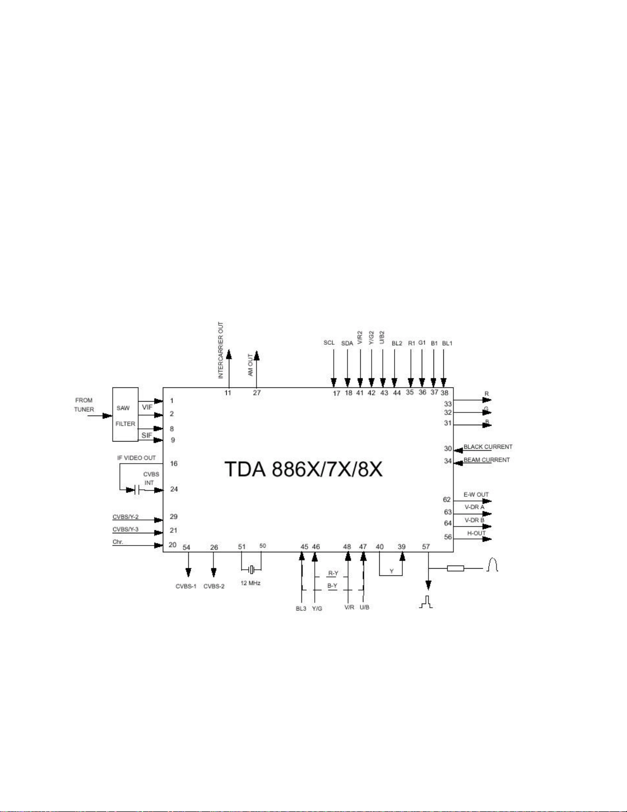
1. INTRODUCTION
11AK33 is a 110ø chassis capable of driving 28-29”,32”,33” tubes at appropriate currents. The chassis have,
Frequency Controlled Tuning (PLL), and control system for multi-standard
(Pal,Secam,BG,DK,L/L’,I/I’,NTSC,M,N ) TV receivers with on-screen-display (OSD) for all relevant
control functions. The system is based on the ‘one-chip’ I2C bus controlled video processing/deflection
IC TDA8885 which also controls sound.
German stereo and Nicam is detected and processed by the MSP 3410 G. Dolby sound is processed by
MSP 3452 G, virtual dolby by MSP 3411G, BTSC Stereo by MSP 3420G (or MSP 3440G ) IC’s by
option. All sound processors also control the sound volume, balance, tone and spatial stereo effect.
The user-interface is menu based control system with cursor keys. Only for some functions the colour
keys are needed: This means that some of the functions can also be operated from the local keyboard
(i.e. Vol -, Vol +, P -, P+ and Menu).
Teletext is done by the microcontroller on-chip teletext module.Fastext/Toptext(8page),One page are
optional.
2. SMALL SIGNAL PART WITH TDA8885
The TDA8885 combines all small signal functions required for a colour TV receiver.
Vision IF amplifier
2.1.
The IF-amplifier contains 3 ac-coupled control stages with a total gain control range, which is higher
then 66 dB. The sensitivity of the circuit is comparable. The video signal is demodulated by means of
an alignment-free PLL carrier regenerator with an internal VCO. This VCO is calibrated by means of a
digital control circuit, which uses the clock frequency of the m-Controller/Teletext decoder as a
reference. The frequency setting for the various standards (33.4, 33.9, 38, 38.9, 45.75 and 58.75 MHz)
is realised via the I 2 C-bus. To get a good performance for phase modulated carrier signals the control
speed of the PLL can be increased by means of the FFI bit. The AFC output is generated by the digital

7
control circuit of the IF-PLL demodulator and can be read via the I 2 C bus. For fast search tuning
systems the window of the AFC can be increased with a factor 3. The setting is realised with the AFW
bit. The AGC-detector operates on top sync and top white-level. The demodulation polarity is switched
via the I 2 C-bus. The AGC detector capacitor is integrated. The time-constant can be chosen via the I 2
C-bus. The time-constant of the AGC system during positive modulation is rather long to avoid visible
variations of the signal amplitude. To improve the speed of the AGC system a circuit has been included
which detects whether the AGC detector is activated every frame period. When during 3 field periods
no action is detected the speed of the system is increased. For signals without peak white information
the system switches automatically to a gated black level AGC. Because a black level clamp pulse is
required for this way of operation the circuit will only switch to black level AGC in the internal mode.
The circuit contains a video identification circuit, which is independent of the synchronisation circuit.
Therefore search tuning is possible when the display section of the receiver is used as a monitor.
However, this Ident circuit cannot be made as sensitive as the slower sync Ident circuit (SL) and we use
both Ident outputs to obtain a reliable search system. The Ident output is supplied to the tuning system
via the I 2 C-bus. The input of the identification circuit is connected to pin 24, the internal CVBS input.
This has the advantage that the Ident circuit can also be made operative when a scrambled signal is
received (descrambler connected between the IF video output (pin 16) and pin 24). A second advantage
is that the Ident circuit can be used when the IF amplifier is not used The video Ident circuit can also be
used to identify the selected CBVS or Y/C signal. The switching between the 2 modes can be realised
with the VIM bit. The IC contains a group delay correction circuit, which can be switched between the
BG and a flat group delay response characteristic. This has the advantage that in multi-standard
receivers no compromise has to be made for the choice of the SAW filter. Also the sound trap is
integrated within the IC .The centre frequency of the trap can be switched via the I 2 C-bus. For monoFM versions it is possible to obtain a demodulated IF video signal which has not passed the sound trap
so that an external stereo decoder can be driven. This function is selected by means of the ICO bit (subaddress 28H). The signal is available on pin 27 (audio output pin when ICO = 0). The S/N ratio of the
selected video signal can be read via the bits SN1/SN0 in sub-address 03H.
2.2. Video Switches
The circuit has an input for the internal CVBS signal and 2 inputs for external CVBS or Y signals. The
circuit has only 1 chroma input so that it is not possible to apply 2 separate Y/C inputs. The selection of
the various sources is made via the I 2 C-bus.Two independently switchable outputs are available. The
CVBS1O output is identical to the selected signal that is supplied to the internal video processing
circuit and which is used as source signal for a teletext decoder. Both CVBS outputs have an amplitude
of 2.0 VP-P . The CVBS2O output is used for CVBS-video output. If the Y/C-3 signal is selected for
one of the outputs the luminance and chrominance signals are added so that a CVBS signal is obtained
again.
2.3. Sound Circuit
The sound IF amplifier is similar to the vision IF amplifier and has a gain control range of about 66 dB.
The AGC circuit is related to the SIF carrier levels (average level of AM or FM carriers) and ensures a
constant signal amplitude of the AM demodulator and the QSS mixer. A multiplier realises the single
reference QSS mixer. In this multiplier the SIF signal is converted to the intercarrier frequency by
mixing it with the regenerated picture carrier from the VCO. The mixer output signal is supplied to the
output via a high-pass filter for attenuation of the residual video signals. With this system a high
performance hi-fi stereo sound processing can be achieved. To optimise the performance of the
demodulator the offset can be compensated by means of an I 2 C-bus setting. The AM sound
demodulator is realised by a multiplier. The modulated sound IF signal is multiplied in phase with the
limited SIF signal. The demodulator output signal is supplied to the output via a low-pass filter for
attenuation of the carrier harmonics. Remark that QSS output pin is 11.
2.4. Synchronisation circuit
The sync separator is preceded by a controlled amplifier, which adjusts the sync pulse amplitude to a
fixed level. These pulses are fed to the slicing stage, which is operating at 50% of the amplitude. The
separated sync pulses are fed to the first phase detector and to the coincidence detector. This
coincidence detector is used to detect whether the line oscillator is synchronised with the incoming
signal and can also be used for transmitter identification. This circuit can be made less sensitive by
means of the STM bit. This mode can be used during search tuning to avoid that the tuning system will

8
stop at very weak input signals. The first PLL has a very high statically steepness so that the phase of
the picture is independent of the line frequency. The horizontal drive signal is generated by an internal
VCO, which is running at a frequency of 25 MHz. This oscillator is stabilised to that frequency by
using the 12 MHz frequency of the crystal oscillator as a reference. The time-constant of the first loop
can be forced by the I 2 C-bus (fast or slow). If required the IC can select the time-constant depending
on the noise content of the incoming video signal. The horizontal output signal is generated by means
of a second loop, which compares the phase of the internal oscillator signal with the phase of the
incoming flyback pulse. The time-constant of this loop is connected externally and can be used as input
for a dynamic horizontal phase correction. To obtain a smooth switch-on and switch-off behaviour of
the horizontal output stage the horizontal drive signal is switched-on and off via the soft-start/soft-stop
procedure. This function is realised by means of a variation of the TON of the horizontal drive pulse.
When the soft-start procedure is completed the horizontal output is gated with the flyback pulse so that
the horizontal output transistor cannot be switched-on during the flyback time. An additional function
of the IC is the ‘low-power start-up’ feature. For this function a supply voltage with a value between 3
and 5 V must be available at the start-up pin (required current 5 mA typical). When all sub-address
bytes have been sent and the POR and XPR flags have been cleared, the horizontal output can be
switched-on via the STB-bit (sub-address 24H). In this condition the horizontal drive signal has the
nominal TOFF and the TON grows gradually from zero to the nominal value as indicated in the softstart behaviour. As soon as the 8 V supply is present the switch-on procedure (e.g. closing of the
second loop) is continued. The presence of the 8 V supply voltage is indicated by the SUP bit in the I 2
C-bus output byte 02. The circuit generates a vertical sync pulse. This pulse can be selected on pin 49
via the bits CMB1 and CMB0. In the 100 Hz input processor versions the vertical sync pulse is
available on pin 63 and the horizontal pulse on pin 56. Via the I C-bus adjustments can be made of the
horizontal and vertical geometry. The vertical sawtooth generator drives the vertical output drive
circuit, which has a differential output current. For the E-W drive a single ended current output is
available. A special feature is the zoom function for both the horizontal and vertical deflection and the
vertical scroll function. When the horizontal scan is reduced to display 4 : 3 pictures on a 16 : 9 picture
tube an accurate video blanking can be switched on to obtain well-defined edges on the screen.
Overvoltage conditions (X-ray protection) can be detected via the EHT tracking pin. When an
overvoltage condition is detected the horizontal output drive signal will be switched-off via the slow
stop procedure but it is also possible that the drive is not switched-off and that just a protection
indication is given in the I 2 C-bus output bytes. The choice is made via the input bit PRD. When PRD
= 1 and an overvoltage is detected the drive is switched-off and the STB bit is set to 0. Switching on of
the drive is only possible when the XPR flag is cleared. The IC has a second protection input on the j2
filter capacitor pin. When this input is activated the drive signal is switched-off immediately and
switched-on again via the slow start procedure. For this reason this protection input can be used as
‘flash protection’. The drive pulses for the vertical sawtooth generator is obtained from a vertical
countdown circuit. This countdown circuit has various windows depending on the incoming signal (50
Hz or 60 Hz and standard or non-standard). The countdown circuit can be forced in various modes by
means of the I 2 C-bus. During the insertion of RGB signals the maximum vertical frequency is
increased to 72 Hz so that the circuit can also synchronise on signals with a higher vertical frequency
like VGA. To obtain short switching times of the countdown circuit during a channel change the
divider can be forced in the search window by means of the NCIN bit. The vertical deflection can be
set in the de-interlace mode via the I 2 C bus.
2.5. Chroma and Luminance processing
The circuit contains a chroma bandpass and trap circuit. The filters are realised by means of gyrator
circuits and they are automatically calibrated by comparing the tuning frequency with the reference
frequency of the decoder. The luminance delay line and the delay for the peaking circuit are also
realised by means of gyrator circuits. The centre frequency of the chroma bandpass filter is switchable
via the I 2 C-bus so that the performance can be optimised for ‘front-end’ signals and external CVBS
signals. During SECAM reception the centre frequency of the chroma trap is reduced to get a better
suppression of the SECAM carrier frequencies.
2.6. Colour Decoder
The colour decoder can decode PAL, NTSC and SECAM signals. The internal clock signals for the
various colour standards are generated by means of an internal VCO, which uses the 12 MHz crystal

9
frequency as a reference. Under bad-signal conditions (e.g. VCR-playback in feature mode), it may
occur that the colour killer is activated although the colour PLL is still in lock. When this killing action
is not wanted it is possible to overrule the colour killer by forcing the colour decoder to the required
standard and to activate the FCO-bit (Forced Colour On) in subaddress 21H. The IC contains an
Automatic Colour Limiting (ACL) circuit which is switchable via the I 2 C-bus and which prevents
that oversaturation occurs when signals with a high chroma-to-burst ratio are received. The ACL circuit
is designed such that it only reduces the chroma signal and not the burst signal. This has the advantage
that the colour sensitivity is not affected by this function. The SECAM decoder contains an autocalibrating PLL demodulator which has two references, viz: the divided 12 MHz reference frequency
of the crystal oscillator which is used to tune the PLL to the desired free-running frequency and the
bandgap reference to obtain the correct absolute value of the output signal. The VCO of the PLL is
calibrated during each vertical blanking period, when the IC is in search or SECAM mode. The
reference frequency of the colour decoder is fed to the Fsc output (pin 49) and is used to tune an
external comb filter. The base-band delay line is integrated. The demodulated colour difference signals
are internally supplied to the delay line. The colour difference matrix switches automatically between
PAL/SECAM and NTSC, however, it is also possible to fix the matrix in the PAL standard.
2.7. PICTURE IMPROVEMENT FEATURES
In the TDA 8885 series various picture improvement features have been integrated. These features are:
-Video dependent coring in the peaking circuit. The coring can be activated only in the low-light parts
of the screen. This effectively reduces noise while having maximum peaking in the bright parts of the
picture.
-Colour Transient Improvement (CTI). This circuit improves the rise and fall times of the colour
difference signals. The function is realised by using delay cells with a length of 300 ns.
-Black-stretch. This circuit corrects the black level for incoming video signals, which have a deviation
between the black level and the blanking, level (back porch). The time constant for the black stretcher
is realised internally
-Blue-stretch. This circuit is intended to shift colour near ‘white’ with sufficient contrast values
towards more blue to obtain a brighter impression of the picture
-White-stretch. This function adapts the transfer characteristic of the luminance amplifier in a nonlinear way dependent on the picture content. The system operates such that maximum stretching is
obtained when signals with a low video level are received. For bright pictures the stretching is not
active.
-Dynamic skin tone (flesh) control. This function is realised in the YUV domain by detecting the
colourss near to the skin tone. The correction angle can be controlled via the I2 C-bus.
RGB output circuit and black-current stabilisation
2.8.
This IC has a very flexible control circuit for RGB input signals, which has the following features:
· Including 3 RGB input, one is dedicated for OSD signals one for scart1,the other one is for RGB
applications.
· The RGB-1 input which is intended for OSD signals and which can be controlled on contrast and
brightness. By means of the IE1 bit the insertion blanking can be switched on or off. Via the IN1 bit it
can be read whether the insertion pin has a high level or not
· To obtain an accurate biasing of the picture tube the ‘Continuous Cathode Calibration’ system has
been included in this IC. Via the I2 C-bus a black level offset can be made with respect to the level
which is generated by the black current stabilisation system. In this way different colour temperatures
can be obtained for the bright and the dark part of the picture.
The black current stabilisation system checks the output level of the 3 channels and indicates whether
the black level of the highest output is in a certain window (WBC-bit) or below or above this window
(HBC-bit). This indication can be read from the I2 C-bus and can be used for automatic adjustment of
the Vg2 voltage during the production of the TV receiver.
The control circuit contains a beam current limiting circuit and a peak white limiting circuit. The peak
white level is adjustable via the I2 C-bus. To prevent that the peak white limiting circuit reacts on the
high frequency content of the video signal a low-pass filter is inserted in front of the peak detector. The
circuit also contains a soft-clipper, which prevents that the high frequency peaks in the output signal
become too high. The difference between the peak white limiting level and the soft clipping level is
adjustable via the I2 C-bus in a few steps.
During switch-off of the TV receiver, the black current control circuit generates a fixed beam current.
This current ensures that the picture tube capacitance is discharged. During the switch-off period the
vertical deflection can be placed in an overseen position so that the discharge is not visible on the
screen.
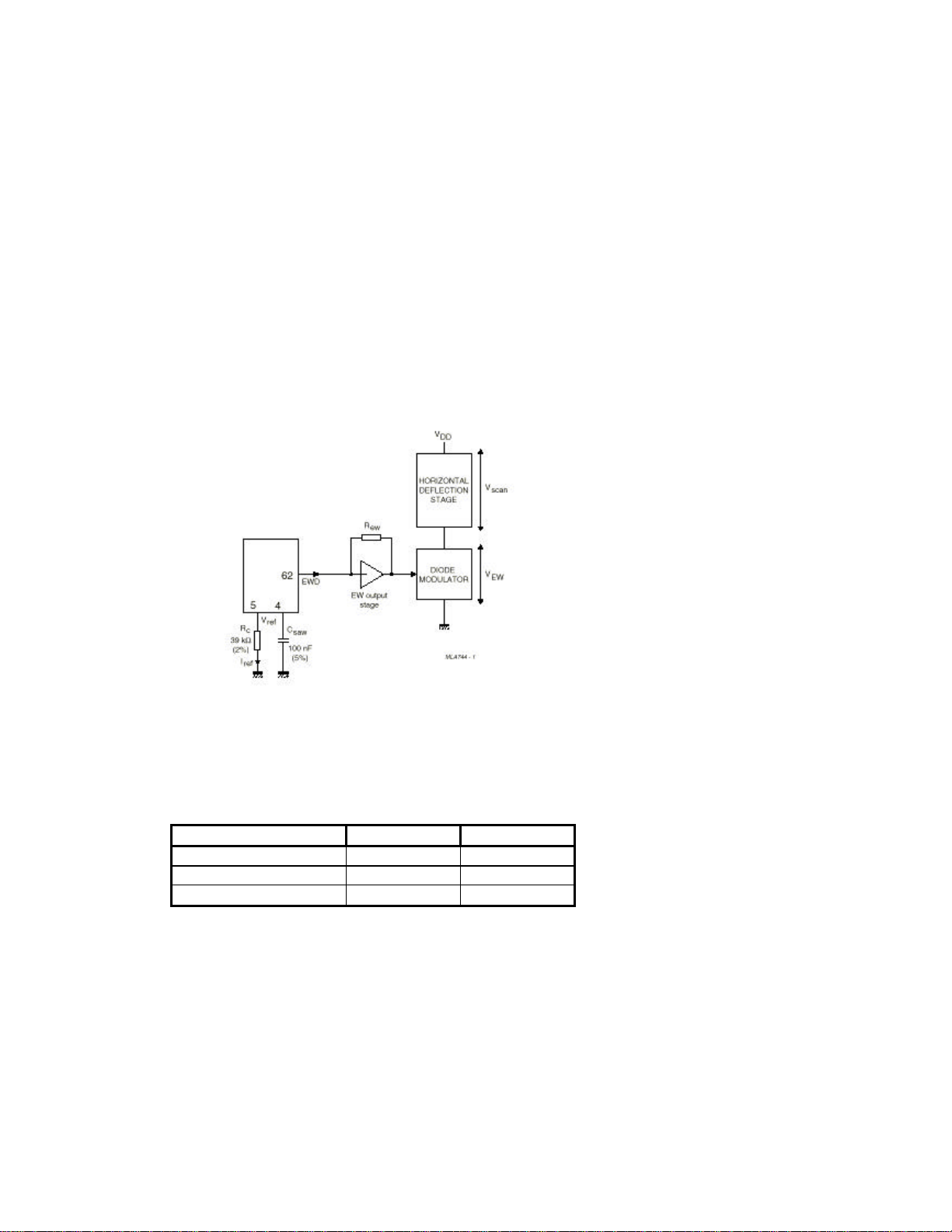
EAST – WEST OUTPUT STAGE
2.9.
In order to obtain correct tracking of the vertical and horizontal EHT-correction, the EW output stage
should be dimensioned as illustrated in Figure. Resistor REW determines the gain of the EW output
stage. Resistor Rc determines the reference current for both the vertical sawtooth generator and the
geometry processor. The preferred value of Rc is 39 kW which results in a reference current of 100 mA
(Vref = 3.9 V).
The value of REW must be:
REW = RC * ( V
/ (18* V
scan
ref
) )
Example: With Vref = 3.9 V; Rc =39 kohm and Vscan = 120 V then REW =68 kohm
2.10 SAW FILTERS
SAW FILTER LIST
SYSTEM&STANDARD VIDEO ( Z 201 ) AUDIO ( Z 200 )
PAL SECAM BG I/I' K3958M K9356
PAL SECAM BG DK L/L' K3953M K9656M
PAL MN NTSC M M3953M M9370
3. TUNER
PLL tuner is used as a tuner.
UV1316 (VHF/UHF) is used as a PLL tuner. For only PALM/N, NTSC M applications UV 1336 are used as the
PLL tuner.
Channel coverage of UV1316:
OFF-AIR CHANNELS CABLE CHANNELS
BAND
CHANNELS FREQUENCY CHANNELS
FREQUENCY
RANGE (MHz)
RANGE (MHz)
10

Low Band E2 to C 48.25 to 82.25 (1) S01 to S08
69.25 to 154.25
Mid Band E5 to E12 175.25 to 224.25 S09 to S38
161.25 to 439.25
High Band E21 to E69 471.25 to 855.25
447.25 to 463.25
(1). Enough margin is available to tune down to 45.25 MHz.
(2). Enough margin is available to tune up to 863.25 MHz.
S39 to S41
(2)
Noise Typical Max. Gain Min. Typical
Max.
Low band : 5dB 9dB All channels : 38dB 44dB
52dB
Mid band : 5dB 9dB Gain Taper (of-air channels) : - 8dB
High band : 6dB 9dB
Channel Coverage UV1336:
BAND CHANNELS FREQUENCY
RANGE (MHz)
Low Band 2 to D 55.25 to 139.25
Mid Band E to PP 145.25 to 391.25
High Band QQ to 69 397.25 to 801.25
Noise is typically 6dB for all channels. Gain is minimum 38dB and maximum 50dB for all channels.
4. VIDEO SWITCH TEA6415C
In case of three or more external sources are used, the video switch IC TEA6415C is used. The main function of
this device is to switch 8 video-input sources on the 6 outputs.
Each output can be switched on only one of each input. On each input an alignment of the lowest level of the
signal is made (bottom of sync. top for CVBS or black level for RGB signals).
Each nominal gain between any input and output is 6.5dB.For D2MAC or Chroma signal the alignment is
switched off by forcing, with an external resistor bridge, 5VDC on the input. Each input can be used as a normal
input or as a MAC or Chroma input (with external Resistor Bridge). All the switching possibilities are changed
through the BUS.
Driving 75ohm load needs an external resistor.
It is possible to have the same input connected to several outputs.
5. MULTI STANDARD SOUND PROCESSOR
The MSP 34x1G family of single-chip Multistandard Sound Processors covers the sound
processing of all analog TV-Standards worldwide, as well as the NICAM digital sound
standards. The full TV sound processing, starting with analog sound IF signal-in, down to processed analog AF-out, is performed on a single chip. signal conforming to the standard by
the Broadcast Television Systems Committee (BTSC).
The DBX noise reduction, or alternatively, MICRONAS Noise Reduction (MNR) is performed
alignment free.
Other processed standards are the Japanese FM-FM multiplex standard (EIA-J) and the FM
Stereo Radio standard.
6. SOUND OUTPUT STAGE WITH TDA 7265
TDA7265 is a class AB dual Audio power amplifier assembled in the multiwatt package.
11

Mute stand-by function of the audio amplifier can be described as the following; the pin 5
(MUTE/STAND-BY) controls the amplifier status by two different thresholds, referred to +Vs. When
Vpin (5) higher than (+Vs - 2.5V) the amplifier is in Stand-by mode and the final stage generators are
off. When Vpin (5) is between (+Vs – 2.5V) and (+Vs – 6V) the final stage current generators are
switched on and the amplifier is in mute mode. When the Vpin (5) is lower than +Vs – 6V the amplifier
is play mode.
7. VERTICAL OUTPUT STAGE WITH STV 9379
The IC TDA9379FA is the vertical deflection booster circuit. Two supply voltages, +14V and –14V are
needed to scan the inputs VERT+ and VERT-, respectively. And a third supply voltage, +60V for the
flyback limiting are needed. The vertical deflection coil is connected in series between the output and
feedback to the input.
8. VIDEO OUTPUT AMPLIFIER TDA6108
The TDA6108Q includes three video output amplifiers is intended to drive the three cathodes of a colour picture
tube.
9. COMBFILTER TDA 9181
The TDA 9181 is an adaptive PAL/NTSC comb filter with two internal delay lines, filters, clock
control, and input clamps. Video standards PAL B, G, H, I, M and N NTSC M are supported.
Two CVBS input signals can be selected by means of input switch.
In addition to the comb filter the circuit contains an output switch so that a selection can be made between the
combed CVBS signal and an external Y/C signal.
The supply voltage is 5V.
10. POWER SUPPLY (SMPS)
The DC voltages required at various parts of the chassis are provided by an SMPS transformer controlled by the IC
MC44608, which is designed for driving, controlling and protecting switching transistor of SMPS. The transformer
produces 150V for FBT input, +/-14V for audio output IC, S+3.3, S+5V and 8V for TDA8885.
11. POWER FACTOR CORRECTION
The MC33260 is a controller for Power Factor Correction pre-converters meeting international
standard requirements in electronic ballast and off–line power conversion applications. Designed to
drive a free frequency discontinuous mode, it can also be synchronised and in any case, it features very
effective protections that ensure a safe and reliable operation.
12. MICROCONTROLLER SDA555X
12.1.
General Features
• Feature selection via special function register
• Simultaneous reception of TTX, VPS, PDC, and WSS (line 23)
• Supply Voltage 2.5 and 3.3 V
• ROM version is used.
12.2. External Crystal and Programmable clock speed
• Single external 6MHz crystal, all necessary clocks are generated internally
• CPU clock speed selectable via special function registers.
• Normal Mode 33.33 MHz CPU clock, Power Save mode 8.33 MHz
12.3. Microcontroller Features
• 8bit 8051 instruction set compatible CPU.
• 33.33-MHz internal clock (max.)
• 0.360 ms (min.) instruction cycle
• Two 16-bit timers
• Watchdog timer
• Capture compare timer for infrared remote control decoding
• Pulse width modulation unit (2 channels 14 bit, 6 channels 8 bit)
12

• ADC (4 channels, 8 bit)
• UART(rxd,txd)
12.4. Memory
• Up to 128 Kilobyte on Chip Program ROM
• Eight 16-bit data pointer registers (DPTR)
• 256-bytes on-chip Processor Internal RAM (IRAM)
• 128bytes extended stack memory.
• Display RAM and TXT/VPS/PDC/WSS-Acquisition-Buffer directly accessible via MOVX
• UP to 16KByte on Chip Extended RAM (XRAM) consisting of;
- 1 Kilobyte on-chip ACQ-buffer-RAM (access via MOVX)
- 1 Kilobyte on-chip extended-RAM (XRAM, access via MOVX) for user software
- 3 Kilobyte Display Memory
12.5. Display Features
• ROM Character set supports all East and West European Languages in single device
• Mosaic Graphic Character Set
• Parallel Display Attributes
• Single/Double Width/Height of Characters
• Variable Flash Rate
• Programmable Screen Size (25 Rows x 33...64 Columns)
• Flexible Character Matrixes (HxV) 12 x 9...16
• Up to 256 Dynamical Redefinable Characters in standard mode; 1024 Dynamical
Redefinable Characters in Enhanced Mode
• CLUT with up to 4096 colour combinations
• Up to 16 Colours per DRCS Character
• One out of Eight Colours for Foreground and Background Colours for 1-bit DRCS and
12.6. ROM Characters
• Shadowing
• Contrast Reduction
• Pixel by Pixel Shiftable Cursor With up to 4 Different Colours
• Support of Progressive Scan and 100 Hz.
• 3 X 4Bits RGB-DACs On-Chip
• Free Programmable Pixel Clock from 10 MHz to 32MHz
• Pixel Clock Independent from CPU Clock
• Multinorm H/V-Display Synchronisation in Master or Slave Mode
12.7. Acquisition Features
• Multistandard Digital Data Slicer
• Parallel Multi-norm Slicing (TTX, VPS, WSS, CC, G+)
• Four Different Framing Codes Available
• Data Caption only limited by available Memory
• Programmable VBI-buffer
• Full Channel Data Slicing Supported
• Fully Digital Signal Processing
• Noise Measurement and Controlled Noise Compensation
• Attenuation Measurement and Compensation
• Group Delay Measurement and Compensation
• Exact Decoding of Echo Disturbed Signals
12.8. Ports
• One 8-bit I/O-port with open drain output and optional I 2 C Bus emulation support (Port0)
• Two 8-bit multifunction I/O-ports (Port1, Port3)
• One 4-bit port working as digital or analogue inputs for the ADC (Port2)
• One 2-bit I/O port with secondary functions (P4.2, 4.3, 4.7)
• One 4-bit I/O-port with secondary function (P4.0, 4.1, 4.4) (Not available in P-SDIP 52)
13
13. SERIAL ACCESS CMOS 8K (1024*8) EEPROM ST24C08
The ST24C08 is a 8Kbit electrically erasable programmable memory (EEPROM), organised as 4 blocks of 256*8
bits.
The memory is compatible with the I²C standard, two wire serial interface, which uses a bi-directional data bus and
serial clock.
The memory carries a built-in 4 bit, unique device identification code (1010) corresponding to the I²C bus
definition.
This is used together with 1 chip enable input (E) so that up to 2*8K devices may be attached to the I²C bus and
selected individually.
14. CLASS AB STEREO HEADPHONE DRIVER TDA1308
The TDA1308 is an integrated class AB stereo headphone driver contained in a DIP8 plastic package.
The device is fabricated in a 1 mm CMOS process and has been primarily developed for portable digital audio
applications.
15. SAW FILTERS
Saw filter type : Model:
K9356M : PAL-SECAM B/G/D/K/I STEREO (AUDIO IF)
K9656M : PAL-SECAM B/G/D/K/I/L/L’ STEREO (AUDIO IF)
K3958M : PAL-SECAM B/G/D/K/I/L/L’ STEREO (VIDEO IF)
16. IC DESCRIPTIONS AND INTERNAL BLOCK DIAGRAM
? TDA8885
? TUNER (UV1315, UV1316)
? TEA6415C
? TDA 7265
? TDA6108Q
? 74HCT32
? MC44608
? SDA5555
? TDA9181
? TCD1102
? ST24C08
? TDA1308
? PCF8583
? MC33260
? STV9379
? MSP34XXG
? LM358N
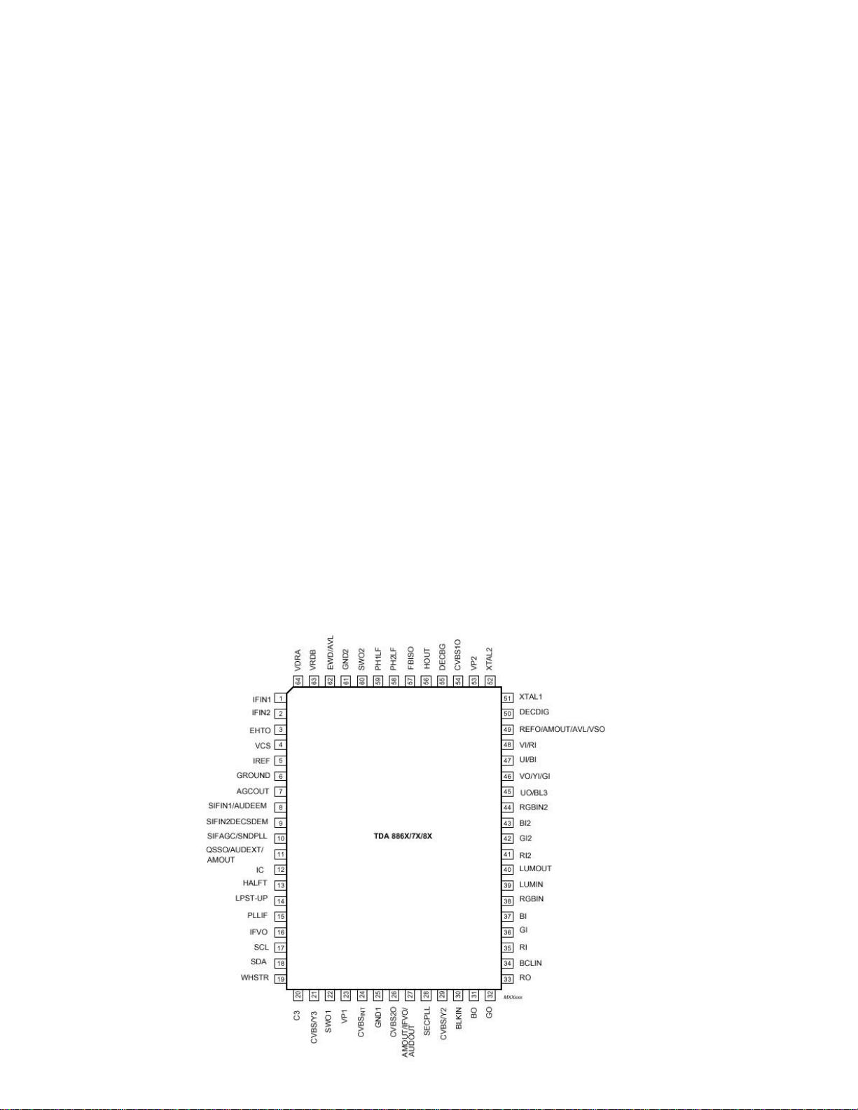
16.1. TDA8885:
14

16.1.1.
The TDA 8885 is I C-bus controlled singlechip TV processor, which is intended to be applied in PAL/NTSC
and multi-standard television receivers. IC contains integrated sound band-pass trap circuits, a switchable
group delay correction circuit and a multi-standard colour decoder which needs only one (12 MHz)
reference crystal for all standards.
Furthermore various picture improvement features have been included.
GENERAL DESCRIPTION
16.1.2. FEATURES
Multi-standard vision IF circuit with an alignment-free PLL demodulator without external components
•
• Internal (switchable) time-constant for the IF-AGC circuit
• Switchable sound trap and group delay correction circuit for the demodulated CVBS signal
• Flexible source selection with CVBS switch and a Y (CVBS)/C input so that a comb filter can be
applied
• Integrated chrominance trap circuit
• Integrated luminance delay line with adjustable delay time
Integrated chroma band-pass filter with switchable centre frequency
•
Colour decoder which needs only one 12 MHz reference crystal (or external clock signal) for all
•
standards
• Blanking of the ‘helper signals’ for PAL
• Several picture improvement features.
• Internal base-band delay line
• Linear RGB input and fast blanking
• RGB control circuit with ‘Continuous Cathode Calibration’, white point and black level offset
adjustment so that the colour temperature of the dark and the light parts of the screen can be chosen
independently.
• Adjustable peak white limiting circuit
• Possibility to insert a ‘blue back’ option when no video signal is available
• Horizontal synchronisation with two control loops and alignment- free horizontal oscillator
• Vertical count -down circuit
• Vertical driver optimised for DC- coupled vertical output stages for improved geometry
Vertical geometry processing.
•
Low-power start-up for the horizontal drive circuit
•
I 2 C-bus control of various functions
•
QSS sound IF amplifier
•
• AM sound demodulator
• PAL decoder
• SECAM decoder
• NTSC decoder
• Additional RGB input
• Black stretch and Blue stretch
• Dynamic skin tone control and coring on complete video signal
• Video dependent coring and Colour Transient Improvement
White stretch and green enhancement
•
Horizontal geometry (EW)
•
• Horizontal and vertical zoom
• Horizontal parallelogram and angle correction
• 2
• Additional YUV/ RGB input with saturation control
• 2 (I 2 C- bus controlled) switch outputs, which can be used to switch external circuits
nd
CVBS output
PLUS
and EDTV-2
16.1.3.
1 IF input 1
2 IF input 2
3 overvoltage protection input
4 vertical sawtooth capacitor
Pin Description
15

5 reference current input
6 ground
7 tuner AGC output
8 SIF input 1
9 SIF input 2
10 narrow-band PLL filter AGC sound IF
11 QSS out
12 internally connected
13 half tone (contrast reduction)
14 low-power start -up
15 IF-PLL loop filter
16 IF video output
17 serial clock input
18 serial data input/output
19 white stretch capacitor
20 chrominance input (S-VHS)
21 external CVBS/Y 3 input
22 output switch 1 (I 2 C)
23 main supply voltage (+8V)
24 internal CVBS input
25 ground 1 (colour decoder and synchronisation)
26 CVBS-2 output
27 audio out (volume controlled) / IF video out
(3)
AM audio output (volume controlled)
28 SECAM PLL decoupling
29 CVBS/Y 2 input
30 black-current input
31 blue output
32 green output
33 red output
34 beam current limiter input/V-guard input
35 red input for insertion
36 green input for insertion
37 blue input for insertion
38 RGB insertion input
39 luminance input
40 luminance output
41 2nd R input
42 2nd G input
43 2nd B input
44 2nd RGB insertion input
45 Additional RGB insertion input
46 Additional G input
47 Additional B signal input
48 Additional R signal input
49 Ref. signal out for comb filter applications.
50 decoupling digital supply
51 12 MHz crystal connection
52 12 MHz crystal connection
53 2nd supply voltage (+8 V) (colour decoder, control, synchronisation and geometry)
54 CVBS-1 output
55 bandgap decoupling
56 horizontal output
57 flyback input / sandcastle output
58 phase-2 filter
59 phase-1 filter
60 output switch 2 (I 2 C)
61 ground 2 (filters, CTI, control and geometry)
62 east-west drive output
63 vertical drive B output
64 vertical drive A output
SYMBOL PARAMETER MIN. TYP. MAX. UNIT
Supply
16
 Loading...