

VESTEL AK30 Service Manual

1
CONTENTS
A. ANALOG PART
SAFETY PRECAUTIONS: ........................................................................................................................................... 3
TV set switched off...................................................................................................................3
Measurements ...........................................................................................................................3
PERI-TV SOCKET ........................................................................................................................................................3
SCART 1 ..................................................................................................................................3
SCART 2 ..................................................................................................................................3
1. INTRODUCTION ......................................................................................................................................................4
2. SMALL SIGNAL PART WITH STV2248 .........................................................................4
2.1 Vision IF amplifier..............................................................................................................4
2.2 QSS Sound circuit (QSS versions) .....................................................................................4
2.3 FM demodulator and audio amplifier (mono versions) ......................................................4
2.4 Video switching ..................................................................................................................5
2.5 Synchronisation circuit .......................................................................................................5
2.6 Chroma and luminance processing .....................................................................................5
2.7 RGB output circuit..............................................................................................................6
2.8 µ-Controller ........................................................................................................................7
3. TUNER ........................................................................................................................................................................7
4- DIGITAL TV SOUND PROCESSOR MSP34X0....................................................................................................8
5. SOUND OUTPUT STAGE TDA7266L/TDA7266 ...................................................................................................8
6. VERTICAL OUTPUT STAGE WITH TDA8174A .................................................................................................8
7. TRIPLE VIDEO OUTPUT AMPLIFIER TDA6107JF ..........................................................................................8
8. POWER SUPPLY (SMPS) ........................................................................................................................................8
9. POWER FACTOR CORRECTION ......................................................................................................................... 8
10. POWER CARD 11PW04-3, 11PW05..…………………………………………………………8
11. RGB SWITCHING CARD 11RGB30-3……………………...………………………………...9
12. SERIAL ACCESS CMOS 8K EEPROM 24C08 ................................................................................................... 9
13. CLASS AB STEREO HEADPHONE DRIVER TDA1308 ................................................................................... 9
14. SAW FILTERS ......................................................................................................................................................... 9
15. IC DESCRIPTIONS AND INTERNAL BLOCK DIAGRAM ............................................................................. 9
ST92195................................................................................................................................10
STV224X ..............................................................................................................................11
UV1315, UV1316, UV1336 ,TECC2949PG40B,TAEA-G0XXD ,ChongQing QingJia .....12
TDA7266/TDA7266L ..........................................................................................................14
TDA8174 ..............................................................................................................................15
TDA6107JF ..........................................................................................................................15
MC44608 ..............................................................................................................................16
MSP34X0G .......................................................................................................................... 17
24C08....................................................................................................................................18
TDA1308 ..............................................................................................................................19
PI5V330………………………………………………………………………………….…20
SAW FILTERS.....................................................................................................................21
SERVICE MENU ADJUSTMENTS ........................................................................................................................... 21
OPTIONS ......................................................................................................................................................................31
GENERAL BLOCK DIAGRAM of 11AK30 .............................................................................................................37
CIRCUIT DIAGRAMS................................................................................................................................................ 38

2
DO NOT CHANGE ANY MODULE UNLESS THE SET IS SWITCHED OFF
The mains supply part of the switch mode power supply’s transformer is live.
Use an isolating transformer.
The receiver complies with the safety requirements.
SAFETY PRECAUTIONS:
The service of this TV set must be carried out by qualified persons only. Components
marked with the warning symbol on the circuit diagram are critical for safety and must only be
replaced with an identical component.
- Power resistor and fused resistors must be mounted in an identical manner to the original
component.
- When servicing this TV, check that the EHT does not exceed 26kV.
TV set switched off:
Make short-circuit between HV-CRT clip and CRT ground layer.
Short C809 before changing IC800 and IC801 or other components in primary side of the SMPS
part.
Measurements:
Voltage readings and oscilloscope traces are measured under the following conditions:
Antenna signal’s level is 60dB at the color bar pattern from the TV pattern generator. (100% white,
75% color saturation)
Brightness, contrast, and color are adjusted for normal picture performance.
Mains supply, 220VAC, 50Hz.
PERI-TV SOCKET
- The figure of PERI-TV socket-
SCART 1 PINING
1 Audio right output 0.5Vrms / 1K
2 Audio right input 0.5Vrms / 10K
3 Audio left output 0.5Vrms / 1K
4 Ground AF
5 Ground Blue
6 Audio left input 0.5Vrms / 10K
7 Blue input 0.7Vpp / 75ohm
8 AV switching input 0-12VDC /10K
9 Ground Green
10 11 Green input 0.7Vpp / 75ohm
12 13 Ground Red
14 Ground Blanking
15 Red input 0.7Vpp / 75ohm
16 Blanking input 0-0.4VDC, 1-3VDC / 75 Ohm
17 Ground CVBS output
18 Ground CVBS input
19 CVBS output 1Vpp / 75ohm
20 CVBS input 1Vpp / 75ohm
21 Ground
SCART 2 PINING
1 Audio right output 0.5Vrms / 1K
2 Audio right input 0.5Vrms / 10K
3 Audio left output 0.5Vrms / 1K
4 Ground AF
5 Ground Blue
6 Audio left input 0.5Vrms / 10K
7 Blue input
8 AV switching input 0-12VDC /10K
9 Ground Green
10 11 12 13 Ground Red
14 Ground Blanking

3
15 16 17 Ground CVBS output
18 Ground CVBS input
19 CVBS output 1Vpp / 75ohm
20 CVBS input 1Vpp / 75ohm
21 Ground
1. INTRODUCTION
11AK30 is a 90° chassis capable of driving 20”/21” tubes at the appropriate currents. The chassis
is capable of operating in PAL, SECAM and NTSC standards. The sound system is capable of
giving 5 watts RMS output into a load of 8 ohms. One page, 7 page SIMPLETEXT, TOPTEXT,
FASTTEXT and US Closed Caption is also provided. The chassis is equipped with a double-deck
42 pin Scart connector.
2. SMALL SIGNAL PART WITH STV2248:
STV2248 video processor is essential for realizing all small signal functions for a color TV
receiver.
2.1 Vision IF amplifier3
The vision IF amplifier can demodulate signals with positive and negative modulation. The PLL
demodulator is completely alignment-free. Although the VCO (Toko-coil) of the PLL circuit is
external, yet the frequency is fixed to the required value by the original manufacturer thus the
Toko-coil does not need to be adjusted manually. The setting of the various frequencies (38.9 or
45.75 MHz) can be made via changing the coil itself.
2.2 QSS Sound circuit (QSS versions)
The sound IF amplifier is similar to the vision IF amplifier and has an external AGC de-coupling
capacitor. The single reference QSS mixer is realised by a multiplier. In this multiplier the SIF
signal is converted to the inter-carrier frequency by mixing it with the regenerated picture carrier
from the VCO. The mixer output signal is supplied to the output via a high-pass filter for
attenuation of the residual video signals. With this system a high performance hi-fi stereo sound
processing can be achieved. The AM sound demodulator is realised by a multiplier. The modulated
sound IF signal is multiplied in phase with the limited SIF signal. The demodulator output signal is
supplied to the output via a low-pass filter for attenuation of the carrier harmonics. The AM signal
is supplied to the output via the volume control.
2.3. AM DEMODULATOR
The AM demodulated signal results from multiplying the input signal by itself, it is available on
AM/FM output.
2.3 FM demodulator and audio amplifier (mono versions):
The FM demodulator is realized as narrow-band PLL with external loop filter, which provides the
necessary selectivity without using an external band-pass filter. To obtain a good selectivity a
linear phase detector and constant input signal amplitude are required. For this reason the intercarrier signal is internally supplied to the demodulator via a gain controlled amplifier and AGC
circuit. The nominal frequency of the demodulator is tuned to the required frequency
(4.5/5.5/6.0/6.5 MHz) by means of a calibration circuit that uses the clock frequency of the µcontroller/Teletext decoder as a reference. The setting to the wanted frequency is realized by means
of the software. It can be read whether the PLL frequency is inside or outside the window and
whether the PLL is in lock or not. With this information it is possible to make an automatic search
system for the incoming sound frequency. This is realized by means of a software loop that
alternate the demodulator to various frequencies, then select the frequency on which a lock

4
condition has been found. De-emphasis output signal amplitude is independent of the TV standard
and has the same value for a frequency deviation of ±25 kHz at the 4.5 MHz standard and for a
deviation of ±50 kHz for the other standards. When the IF circuit is switched to positive
modulation the internal signal on de-emphasis pin is automatically muted. The audio control
circuit contains an audio switch and volume control. In the mono inter-carrier sound versions the
Automatic Volume Leveling (AVL) function can be activated. The pin to which the external
capacitor has to be connected depends on the IC version. For the 90° types the capacitor is
connected to the EW output pin (pin 20). When the AVL is active it automatically stabilizes the
audio output signal to a certain level.
2.4 Video switching
The video processor (STV2248C) has three CVBS inputs and two RGB inputs. The first CVBS
input is used for external CVBS from SCART 1, the second is used for either CVBS or Y/C from
either SCART2 or BAV/FAV, and the third one is used for internal video. The selection between
both external video inputs signals is realized by means of software and hardware switches.
2.5 Synchronization circuit
The video processor (STV224X) performs the horizontal and vertical processing. The external
horizontal deflection circuit is controlled via the Horizontal output pulse (HOUT). The vertical
scanning is performed through an external ramp generator and a vertical power amplifier IC
controlled by the Vertical output pulse (VOUT).
The main components of the deflection circuit are:
• PLL1: the first phase locked loop that locks the internal line frequency reference on the
CVBS input signal. It is composed of an integrated VCO (12 MHz) that requires the chroma
Reference frequency (4.43MHz or 3.58MHz crystal oscillator reference signal), a divider by
768, a line decoder, and a phase comparator.
• PLL2: The second phase locked loop that controls the phase of the horizontal output
(Compensation of horizontal deflection transistor storage time variation). Also the horizontal
position adjustment is also performed in PLL2.
• A vertical pulse extractor.
• A vertical countdown system to generate all vertical windows (vertical synchronization
window, frame blanking pulses, 50/60Hz identification window...).
• Automatic identification of 50/60Hz scanning.
• PLL1 time constant control.
• Noise detector, video identification circuits, and horizontal coincidence detector.
• Vertical output stage including de-interlace function, vertical position control.
• Vertical amplitude control voltage output (combined with chroma reference output and
Xtal 1 indication).
2.6 Chroma and luminance processing:
The chroma decoder is able to demodulate PAL, NTSC and SECAM signals.
The decoder dedicated to PAL and NTSC sub-carrier is based on a synchronous demodulator,
and an Xtal PLL locked on the phase reference signal (burst).
The SECAM demodulation is based on a PLL with automatic calibration loop.
The color standard identification is based on the burst recognition.
Automatic and forced modes can be selected through the I2C bus.
NTSC tint, and auto flesh are controlled through I2C bus.
Xtal PLL can handle up to 3 crystals to work in PAL M, PAL N and NTSC M for South America.
ACC an ACC overload control the chroma sub-carrier amplitude within 26dB range. Both

5
ACC s are based on digital systems and do not need external capacitor.
All chroma filters are fully integrated and tuned via a PLL locked on Xtal VCO signal.
A second PLL is used for accurate fine-tuning of the SECAM bell filter. This tuning is achieved
during the frame blanking. An external capacitor memorizes the bell filter tuning voltage.
A base-band chroma delay-line rebuilds the missing color line in SECAM and removes
transmission phase errors in PAL.
The base-band chroma delay line is clocked with 6MHz signal provided by the horizontal scanning
VCO.
The luminance processor is composed of a chroma trap filter, a luminance delay line, a peaking
function with noise coring feature, a black stretch circuit.
Trap filter and luminance delay lines are achieved with the use of bi-quad integrated filters, autoaligned via a master filter phase locked loop.
2.7 RGB output circuit:
The video processor performs the R, G, B processing.
There are three sources:
1. Y,U,V inputs (coming from luma part (Y output), and chroma decoder outputs (R-Y, B-Y
outputs).
2. External R,G,B inputs from SCART (converted internally in Y,U,V), with also the possibility
to input YUV signals from a DVD player, (YUV specification is Y=0.7 V PP , U= 0.7 V PP ,
V = 0.7V PP for 100% color bar).
3. Internal R,G,B inputs (for OSD and Teletext display)
The main functions of the video part are:
- Y,U,V inputs with integrated clamp loop, allowing a DC link with YUV outputs,
- External RGB inputs (RGB to YUV conversion), or direct YUV inputs,
- Y,U,V switches,
- Contrast, saturation, brightness controls,
- YUV to RGB matrix,
- OSD RGB input stages (with contrast control),
- RGB switches,
- APR function,
- DC adjustment of red and green channels,
- Drive adjustments (R, G, B gain),
- Digital automatic cut-off loop control,
- Manual cut-off capability with I2C adjustments,
- Half tone, oversize blanking, external insertion detection, blue screen,
- Blanking control and RGB output stages.
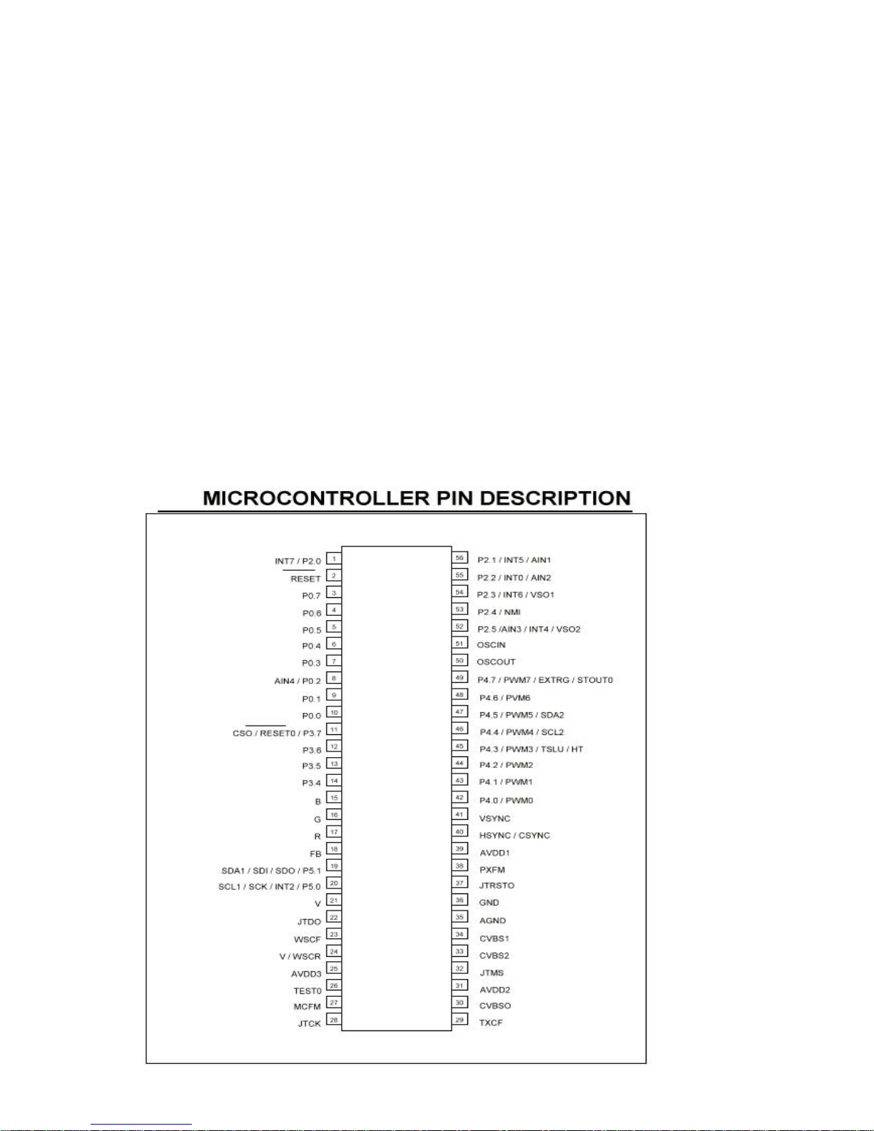
2.8 µ-Controller
The ST92195 is the micro-controller, which is required for a color TV receiver. ST92195D1 is the
version with one page Teletext and ST92195D7 is the one with 7 page Teletext. The IC has the
supply voltages of 5 V and they are mounted in PSDIP package with 56 pins.
µ-Controller has the following features
Display of the program number, channel number, TV Standard, analogue values, sleep timer,
parental control and mute is done by OSD
Single LED for standby and on mode indication
System configuration with service mode
3 level logic output for SECAM and Tuner band switching
6
3. TUNER
Either a PLL or a VST tuner is used as a tuner.
UV1316 (VHF/UHF) is used as a PLL tuner. For only PALM/N, NTSC M applications UV 1336
is used as the PLL tuner. UV 1315 (VHF/UHF) is used as a VST Tuner.
Channel coverage of UV1316:
BAND
OFF-AIR CHANNELS
CHANNELS FREQUENCY
RANGE (MHz)
CABLE CHANNELS
CHANNELS FREQUENCY
RANGE (MHz)
Low Band E2 to C 48.25 to 82.25 (1) S01 to S08 69.25 to 154.25
Mid Band E5 to E12 175.25 to 224.25 S09 to S38 161.25 to 439.25
High Band E21 to E69 471.25 to 855.25 (2) S39 to S41 447.25 to 463.25
(1). Enough margin is available to tune down to 45.25 MHz.
(2). Enough margin is available to tune up to 863.25 MHz.
Noise Typical Max. Gain Min. Typical Max.
Low band : 5dB 9dB All channels : 38dB 44dB 52dB
Mid band : 5dB 9dB Gain Taper (of-air channels): 8dB
High band : 6dB 9dB
Channel Coverage UV1336:
BAND CHANNELS FREQUENCY
RANGE (MHz)
Low Band 2 to D 55.25 to 139.25
Mid Band E to PP 145.25 to 391.25
High Band QQ to 69 397.25 to 801.25
Noise is typically 6dB for all channels. Gain is minimum 38dB and maximum 50dB for all
channels.
Channel Coverage of UV1315:
BAND
OFF-AIR CHANNELS
CHANNELS FREQUENCY
RANGE (MHz)
CABLE CHANNELS
CHANNELS FREQUENCY
RANGE (MHz)
Low Band E2 to C 48.25 to 82.25 (1) S01 to S10 69.25 to 168.25
Mid Band E5 to E12 175.25 to 224.25 S11 to S39 231.25 to 447.25
High Band E21 to E69
471.25 to 855.25 (2)
S40 to S41 455.25 to 463.25
(1). Enough margin is available to tune down to 45.25 MHz.
(2). Enough margin is available to tune up to 863.25 MHz.

7
Noise Typ. Max. Gain Min. Typ. Max.
Low band 6dB 9dB All Channels 38dB 44dB 50dB
Mid band 6dB 10dB Gain Taper 8dB
High band 6dB 11dB (off-air channels)
4. DIGITAL TV SOUND PROCESSOR MSP34X0
The MSP 34x0D is designed to perform demodulation of FM or AM-Mono TV sound.
Alternatively, two-carrier FM systems according to the German or Korean terrestrial specs or the
satellite specs can be processed with the MSP 34x0D. Digital demodulation and decoding of
NICAM-coded TV stereo sound, is done only by the MSP 3410. The MSP 34x0D offers a
powerful feature to calculate the carrier field strength which can be used for automatic standard
detection (terrestrial) and search algorithms (satellite).
5. SOUND OUTPUT STAGE TDA7266L/TDA7266
TDA7266L is used as the AF output amplifier for mono applications. It is supplied by +12VDC
coming from a separate winding in the SMPS transformer. An output power of 5.5W (THD=0.5%)
can be delivered into an 8ohm load.
TDA7266 is used as the AF output amplifier for stereo applications. It is supplied by
+12VDC coming from a separate winding in the SMPS transformer. An output power of 2*5.5W
(THD=0.5%) can be delivered into an 8ohm load.
6. VERTICAL OUTPUT STAGE WITH TDA8174A
The TDA8174A is a power amplifier circuit for use in 90° and 110° colour deflection systems for
25 to 200 Hz field frequencies, and for 4 : 3 and 16 : 9 picture tubes.
7. TRIPLE VIDEO OUTPUT AMPLIFIER TDA6107JF
The TDA6107JF includes three video output amplifiers and is intended to drive the three cathodes
of a colour CRT directly. The device is contained in a plastic DIL-bent-SIL 9-pin medium power
(DBS9MPF) package, and uses high-voltage DMOS technology.
To obtain maximum performance, the amplifier should be used with black-current control.
Inputs and outputs are protected against electrostatic discharge in normal handling. However, to be
totally safe, it is desirable to take normal precautions appropriate to handling MOS devices.
8. POWER SUPPLY (SMPS)
The DC voltages required at various parts of the chassis are provided by an SMPS transformer
controlled by the IC MC44608 which is designed for driving, controlling and protecting switching
transistor of SMPS. The transformer produces 115V for FBT input, 14V for audio output IC,
S+3.3, S+5V and 8V for ST92195.
9. POWER FACTOR CORRECTION
Passive components are used for the solution of power factor correction.
10. POWER CARD
Power cards are used to supply DC voltages required for DVD box inside AK30 TV.
11PW04-3 card produces +3.3V, +2.5V, +5V DC voltages for DVD boxes.

8
11. RGB SWITCHING CARD 11RGB30-3
RGB Switching Card is used to switch R_EXT, G_EXT, B_EXT and R_DVDorDVB,
G_DVDorDVB, B_DVDorDVB between each other to provide one R_OUT, G_OUT, B_OUT for
output. PI5V330 Low On-Resistance Wideband/Video Quad 2-Channel Mux/DeMux IC is used to
ensure switching operation.
10. SERIAL ACCESS CMOS 8K EEPROM 24C08
The 24C08 is a 8Kbit electrically erasable programmable memory (EEPROM), organized as 4
blocks of 256*08 bits. The memory is compatible with the I²C standard, two wire serial interface
which uses a bi-directional data bus and serial clock.
11. CLASS AB STEREO HEADPHONE DRIVER TDA1308
The TDA1308 is an integrated class AB stereo headphone driver contained in a DIP8 plastic
package
12. SAW FILTERS
Saw filter type: Model:
G1975M: PAL B/G MONO
K2966M: PAL SECAM B/G/D/K/I MONO
J1981 : PAL-I MONO
K2958M: PAL-SECAM B/G-D/K (38) MONO
K2962M: PAL-SECAM B/G/D/K/I/L/L’ MONO
L9653M: SECAM L/L’ AM MONO (AUDIO IF)
G3967M: PAL-SECAM B/G STEREO (VIDEO IF)
G9353M: PAL-SECAM B/G STEREO (AUDIO IF)
K3958M: PAL-SECAM B/G/D/K/I/L/L’ STEREO (VIDEO IF)
K9356M: PAL-SECAM B/G/D/K/I STEREO (AUDIO IF)
K9656M: PAL-SECAM B/G/D/K/I/L/L’ STEREO (AUDIO IF)
K3958M: PAL I NICAM (VIDEO IF)
K9356M: PAL I NICAM (AUDIO IF)
M1962M: PAL M/N NTSC M MONO
M3953M: PAL M/N NTSC M STEREO (VIDEO IF)
M9370M: PAL M/N NTSC M STEREO (AUDIO IF)
13. IC DESCRIPTIONS AND INTERNAL BLOCK DIAGRAM
ST92195
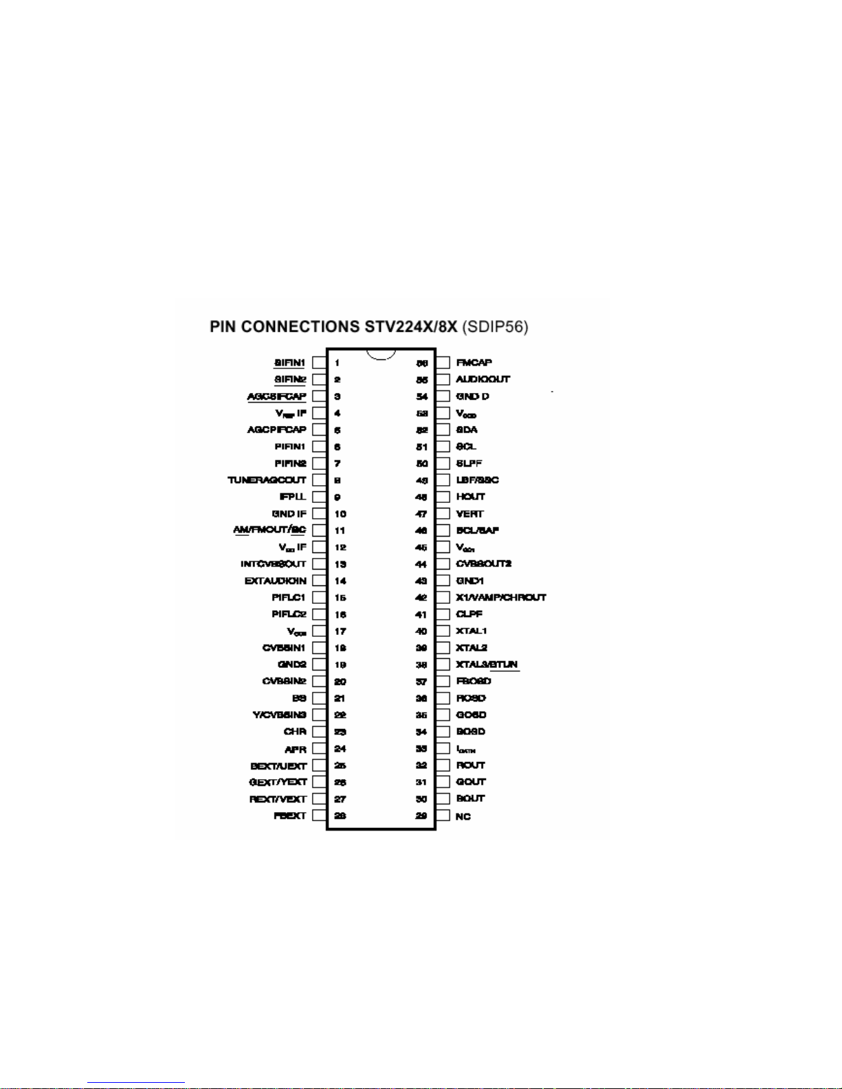
STV224X
TUNER (UV1315, UV1316, UV1336,TECC2949PG40B,TAEA-G0XXD ,ChongQing QingJia)
TDA7266L / TDA7266M
TDA8174A
TDA6107JF
MC44608
MSP34X0D
24C08
TDA1308
9
SAW FILTERS
G1975M, K2966M, K2962M, L9653M, G3962M, G9353M, K3958M, K9356M, K9656M,
K6263K, K9652M,
M1962M, M3953M, M9370M
ST92195
The ST92195 is a member of the ST9+ family of micro-controllers, completely developed and
produced by SGS-THOMSON Microelectronics using a proprietary n-well HCMOS process. The
nucleus of the ST92195 is the advanced Core, which includes the Central Processing Unit (CPU),
the ALU, the Register File and the interrupt controller. The Core has independent memory and
register buses to add to the efficiency of the code. A set of on-chip peripherals form a complete
sys-tem for TV set and VCR applications:
– Voltage Synthesis
– VPS/WSS Slicer
– Teletext Slicer
– Teletext Display RAM
– OSD
Additional peripherals include a watchdog timer , a serial peripheral interface (SPI), a 16-bit timer
and
an A/D converter.
10
STV224X Video processor:
The STV2246/2247/2248 are fully bus controlled ICs for TV including PIF, SIF, luma, Chroma
and deflection processing. Used with a vertical frame booster (TDA1771 or TDA8174 for 90°
chassis, STV9306 for 110° chassis), they allow the design of multi-standard (BGDKIMNLL, PAL/
SECAM/NTSC) sets with very few external components and no manual adjustments.

11
UV1315, UV1316, UV1336,TECC2949PG40B,TAEA-G0XXD ,ChongQing QingJia
General description of UV1315:
The UV1315 tuner belongs to the UV 1300 family of tuners, which are designed to meet a wide
range of applications. It is a combined VHF, UHF tuner suitable for CCIR systems B/G, H, L, L’, I
and I’.
Features of UV1315:
Member of the UV1300 family small sized UHF/VHF tuners
Systems CCIR:B/G, H, L, L’, I and I’; OIRT:D/K
Voltage synthesized tuning (VST)
Off-air channels, S-cable channels and Hyper-band
Standardized mechanical dimensions and pinning
PINNING PIN VALUE
1. Gain control voltage (AGC) :4.0V, Max:4.5V
2. Tuning voltage
3. High band switch :5V, Min:4.75V, Max:5.5V
4. Mid band switch :5V, Min:4.75V, Max:5.5V
5. Low band switch :5V, Min:4.75V, Max:5.5V
6. Supply voltage :5V, Min:4.75V, Max:5.5V
7. Not connected
8. Not connected
9. Not connected
10. Symmetrical IF output 1
11. Symmetrical IF output 2
Band switching table:
Pin 3 Pin 4 Pin 5
Low band 0V 0V +5V
Mid band 0V +5V 0V
High band +5V 0V 0V
General description of UV1316:
The UV1316 tuner belongs to the UV 1300 family of tuners, which are designed to meet a wide
range of applications. It is a combined VHF, UHF tuner suitable for CCIR systems B/G, H, L, L’, I
and I’.
Features of UV1316:
Member of the UV1300 family small sized UHF/VHF tuners
Systems CCIR: B/G, H, L, L’, I and I’; OIRT: D/K
Digitally controlled (PLL) tuning via I²C-bus
Off-air channels, S-cable channels and Hyper-band
World standardized mechanical dimensions and world standard pinning
Complies to “CENELEC EN55020” and “EN55013”

12
PINNING PIN VALUE
1. Gain control voltage (AGC) :4.0V, Max:4.5V
2. Tuning voltage
3. I²C-bus address select :Max:5.5V
4. I²C-bus serial clock :Min:-0.3V, Max:5.5V
5. I²C-bus serial data :Min:-0.3V, Max:5.5V
6. Not connected
7. PLL supply voltage :5.0V, Min:4.75V, Max:5.5V
8. ADC input
9. Tuner supply voltage :33V, Min:30V, Max:35V
10. Symmetrical IF output 1
11. Symmetrical IF output 2
General description of UV1336:
UV1336 series is developed for reception of channels broadcast in accordance with the M, N
standard.
Features of UV1336:
Global standard pinning
Integrated Mixer-Oscillator & PLL function
Conforms to CISPR 13, FCC and DOC (Canada) regulations
Low power consumption
Both Phono connector and ‘F’ connector are available
PINNING PIN VALUE
1. Gain control voltage :4.0V, Max:4.5V
2. Tuning voltage
3. Address select Max:5.5V
4. Serial clock :Min:-0.3V, Max:5.5V
5. Serial data :Min:-0.3V, Max:5.5V
6. Not connected
7. Supply voltage :5.0V, Min:4.75V, Max:5.5V
8. ADC input (optional)
9. Tuning supply voltage :33V, Min:30V, Max:35V
10. Ground
11. IF output

TECC2949PG40B SAMSUNG TUNER
Features:
• CCIR standart receiving system
•Off- air channels ,s-cable channels , 3 band (UHF,VHFhigh and low)
• PAL FST tuner
•Tuning system :Frequency synthesized type
Pinning:
1- AGC AGC Voltage supply (Typ:5V Max:4.5V)
2- NC No pin
3- SAS Adress select
4- SCL Serial clock
5- SDA Serial data
6- NC No pin
7- BP B+ for internal IC (Min:4.75V Typ:5V Max.5.5V)
8- NC No pin
9- BT Tuning supply voltage (Min:30V Typ:33V Max: 35V)
10- IF2 IF output2
11- IF1 IF1 output
TAEA-G0XXD LG TUNER
Features:
• CCIR+CATV standart receiving channel
•Off- air channels ,s-cable channels , 3 band (UHF,VHFhigh and low)
•Upper heterodyne Receiving system
•Varactor –Tuned(With PLL)
Pinning:
1- AGC AGC Voltage supply (Typ:5V Max:4.5V)
2- TU Tuning output voltage
3- SAS Adress select
4- SCL Serial clock
5- SDA Serial data
6- B+ No pin
7- B+ B+ for internal IC (Min:4.75V Typ:5V Max.5.5V)
8- NC No pin
9- BT Tuning supply voltage (Min:30V Typ:33V Max: 35V)
10- IF2 IF output2
11- IF1 IF1 output

ChongQing QingJia Electronical Co.Tuner
•PAL BG Receiving system
•PLL tuning system
•Off- air channels ,s-cable channels , 3 band (UHF,VHFhigh and low)
Pinning:
1- AGC AGC Voltage supply (Typ:5V Max:4.5V)
2- NC No pin
3- SAS Adress select
4- SCL Serial clock
5- SDA Serial data
6- NC No pin
7- BP B+ for internal IC (Min:4.75V Typ:5V Max.5.5V)
8- NC No pin
9- BT Tuning supply voltage (Min:30V Typ:33V Max: 35V)
10- IF2 IF output2
11- IF1 IF1 output

13
TDA7266/TDA7266L
General Description of TDA7266L
The TDA7266L is a mono bridge amplifier specially designed for TV and Portable Radio
applications. Requires very few external components
WIDE SUPPLY VOLTAGE RANGE (3-18V)
MINIMUM EXTERNAL COMPONENTS
– NO SVR CAPACITOR
– NO BOOTSTRAP
– NO BOUCHEROT CELLS
– INTERNALLY FIXED GAIN
STAND-BY & MUTE FUNCTIONS
SHORT CIRCUIT PROTECTION
THERMAL OVERLOAD PROTECTION
PINNING
1 N.C.
2 N.C.
3 MUTE
4 ST-BY
5 PW-GND
6 S-GND
7 IN
8 VCC
9 OUT+
10 OUT -
General Description of TDA7266
The TDA7266 is a 2x7 Watt dual power amplifier. It is used for sound amplification at stereo TV
sets.
WIDE SUPPLY VOLTAGE RANGE (3-18V)
MINIMUM EXTERNAL COMPONENTS
– NOSWR CAPACITOR
– NOBOOTSTRAP
– NOBOUCHEROT CELLS
– INTERNALLY FIXED GAIN
STAND-BY & MUTE FUNCTIONS
SHORT CIRCUIT PROTECTION
THERMAL OVERLOAD PROTECTION
PINNING
1. OUT1+
2. OUT1 –
3. VCC
4. IN1
5. N.C.
6. MUTE
7. ST-BY
8. PW-GND

14
9. S-GND
10. N.C.
11. N.C.
12. IN2
13. VCC
14. OUT2 -
15. OUT2+
TDA8174AW
INDEPENDENT VERTICAL AMPLITUDE ADJUSTEMENT. BUFFER STAGE. POWER
AMPLIFIER
.FLYBACKGENERATOR .THERMALPROTECTION .INTERNAL REFERENCE VOLTAGE
DECOU-PLING
General Description:
TDA8174Aand TDA8174AWare a monolithic integrated circuits. It is a full performance and very
efficient vertical deflection circuit intended for direct drive of a TV picture tube in Color and B &
W television as well as in Monitor and Data displays.
PINNING
1. POWER OUTPUT
2. OUTPUT STAGE Vs
3. TRIGGER INPUT
4. HEIGHT ADJUSTMENT
5. VOLTAGE REF DECOUPLING
6. GROUND
7. RAMP GENERATOR
8. BUFFER OUTPUT
9. INVERTING INPUT
10. Vs
11. FLYBACK GENERATOR
TDA6107JF
General Description:
The TDA6107JF includes three video output amplifiers and is intended to drive the three cathodes
of a colour CRT directly. The device is contained in a plastic DIL-bent-SIL 9-pin medium power
(DBS9MPF) package, and uses high-voltage DMOS technology.
To obtain maximum performance, the amplifier should be used with black-current control.
FEATURES
· Typical bandwidth of 5.5 MHz for an output signal of 60 V (p-p)
· High slew rate of 900 V/ms
· No external components required
· Very simple application

15
· Single supply voltage of 200 V
· Internal reference voltage of 2.5 V
· Fixed gain of 50
· Black-Current Stabilization (BCS) circuit with voltage window from 1.8 to 6 V and current
window from -100 mA to 10 mA
· Thermal protection
· Internal protection against positive flashover discharges appearing on the CRT.
PINNING
SYMBOL PIN DESCRIPTION
Vi(1) 1 inverting input 1
Vi(2) 2 inverting input 2
Vi(3) 3 inverting input 3GND 4 ground (fin)
Iom 5 black-current measurement output
VDD 6 supply voltage
Voc(3) 7 cathode output 3
Voc(2) 8 cathode output 2
Voc(1) 9 cathode output 1
MC44608
General description:
The MC44608 is a high performance voltage-mode controller designed for off–line converters.
This high voltage circuit that integrates the start–up current source and the oscillator capacitor,
requires few external components while offering a high flexibility and reliability.
The device also features a very high efficiency stand–by management consisting of an effective
Pulsed Mode operation. This technique enables the reduction of the stand–by power consumption
to approximately 1W while delivering 300mW in a 150W SMPS.
• Integrated start–up current source
• Loss less off–line start–up
• Direct off–line operation
• Fast start–up
General Features
• Flexibility
• Duty cycle control
• On chip oscillator switching frequency 40, or 75kHz
• Secondary control with few external components
Protections
• Maximum duty cycle limitation
• Cycle by cycle current limitation
• Demagnetization (Zero current detection) protection
• “Over V CC protection” against open loop
• Programmable low inertia over voltage protection against open loop
• Internal thermal protection

16
GreenLine Controller
• Pulsed mode techniques for a very high efficiency low power mode
• Lossless startup
• Low dV/dT for low EMI radiations
PINNING PIN VALUE
1. Demagnetization Zero cross detection voltage: 50 mV typ.
2. I Sense Over current protection voltage 1V typ.
3. Control Input Min: 7.5V Max.: 18V
4. Ground Iout 2A
p-p
during scan 1.2A
p-p
during flyback
5. Driver Output resistor 8.5 Ohm sink 15 Ohm source typ.
6. Supply voltage Max:16V (Operating range 6.6V-13V)
7. No connection
8. Line Voltage Min:50V Max:500V
MSP34X0D
The MSP 34x0D is designed to perform demodulation of FM or AM-Mono TV sound. Two kinds
of MSP’s are used. MSP 3400D and MSP 3410D. The MSP 3400D is fully pin and softwarecompatible to the MSP 3410D, but is not able to decode NICAM. It is also compatible to the MSP
3400C.
General description:
Demodulator and NICAM Decoder Section
The MSP 34x0D is designed to perform demodulation of FM or AM-Mono TV sound.
Alternatively, two-carrier FM systems according to the German or Korean terrestrial specs or the
satellite specs can be processed with the MSP 34x0D. Digital demodulation and decoding of
NICAM-coded TV stereo sound, is done only by the MSP 3410. The MSP 34x0D offers a
powerful feature to calculate the carrier field strength, which can be used for automatic standard
detection (terrestrial) and search algorithms (satellite).
General Features
Two selectable analog inputs (TV and SAT-IF sources)
Automatic Gain Control (AGC) for analog IF input. Input range: 0.10–3 V pp
Integrated A/D converter for sound-IF inputs
All demodulation and filtering is performed on chip and is individually programmable
Easy realization of all digital NICAM standards (B/G, D/K, I & L) with MSP 3410G.
FM demodulation of all terrestrial standards (incl. identification decoding)
FM demodulation of all satellite standards
No external filter hardware is required
Only one crystal clock (18.432 MHz) is necessary
FM carrier level calculation for automatic search algorithms and carrier mute function
DSP Section (Audio Base band Processing)
Flexible selection of audio sources to be processed
Two digital input and one output interface via I 2 S bus for external DSP processors, featuring
surround sound, ADR etc.

17
Digital interface to process ADR (ASTRA Digital Radio) together with DRP 3510A
Performance of all de-emphasis systems including adaptive Wegener Panda 1 without external
components or controlling
Digitally performed FM identification decoding and de-matrixing
Digital base-band processing: volume, bass, treble, 5-band equalizer, loudness, pseudo-stereo,
and base-width enlargement
Simple controlling of volume, bass, treble, equalizer etc.
Analog Section
four selectable analog pairs of audio base-band inputs (= four SCART inputs) input level: =<2
V RMS , input impedance: >=25 k
one analog mono input (i.e. AM sound): input level: =<2 V RMS , input impedance: >=15 k
two high-quality A/D converters, S/N-Ratio: >=85 dB
20 Hz to 20 kHz bandwidth for SCART-to-SCART copy facilities
24C08
General description:
The 24C16 is a 8Kbit electrically erasable programmable memory (EEPROM), organized as 4
blocks of 256 * 08 bits. The memory operates with a power supply value as low as 2.5V.
Features:
Minimum 1 million ERASE/WRITE cycles with over 10 years data retention
Single supply voltage:4.5 to 5.5V
Two wire serial interface, fully I²C-bus compatible
Byte and Multi-byte write (up to 8 bytes)
Page write (up to 16 bytes)
Byte, random and sequential read modes
Self timed programming cycle
PINNING PIN VALUE
1. Write protect enable :0V
2. Not connected :0V
3. Chip enable input :0V
4. Ground :0V
5. Serial data address input/output :Input LOW voltage: Min:-0.3V, Max:0.3*Vcc
:Input HIGH voltage: Min:0.7*Vcc, Max:Vcc+1
6. Serial clock :Input LOW voltage: Min:-0.3V, Max:0.3*Vcc
:Input HIGH voltage: Min:0.7*Vcc, Max:Vcc+1
7. Multibyte/Page write mode :Input LOW voltage: Min:-0.3V, Max:0.5V
:Input HIGH voltage: Min:Vcc-0.5, Max:Vcc+1
8. Supply voltage :Min:2.5V, Max:5.5V

18
TDA1308
Features:
Wide temperature range
Excellent power supply ripple rejection
Low power consumption
Short-circuit resistant
High performance
high signal-to-noise ratio
low distortion
PINNING PIN VALUE
1. Output A (Voltage swing) :Min:0.75V, Max:4.25V
2. Inverting input A :Vo(clip):Min:1400mVrms
3. Non-inverting input A :2.5V
4. Ground :0V
5. Non-inverting input B :2.5V
6. Inverting input B :Vo(clip):Min:1400mVrms
7. Output B (Voltage swing) :Min:0.75V, Max:4.25V
8. Positive supply :5V, Min:3.0V, Max:7.0V
PI5V330
Description
Pericom Semiconductor’s PI5V330 is a true bidirectional Quad 2-channel
multiplexer/demultiplexer recommended for both RGB and composite video switching
applications. The video switch can be driven from a current output RAMDAC or voltage output
composite video source.
Low On-Resistance and wide bandwidth make it ideal for video and other applications. Also this
device has exceptionally high current capability which is far greater than most analog switches
offered today. A single 5V supply is all that is required for operation.
The PI5V330 offers a high-performance, low-cost solution to switch between video sources. The
application section describes the PI5V330 replacing the HC4053 multiplier and buffer/amplifier.
Features
• High-performance solution to switch between video sources
• Wide bandwidth: 200 MHz
• Low On-Resistance: 3Ω
• Low crosstalk at 10 MHz: –58dB
• Ultra-low quiescent power (0.1μA typical)
• Single supply operation: +5.0V
• Fast switching: 10ns
• High-current output: 100mA
• Packaging (Pb-free & Green Available):– 16-pin 300-mil wide plastic SOIC (S)
19
– 16-pin 150-mil wide plastic SOIC (W)
– 16-pin 150-mil wide plastic QSOP (Q)
Saw filter’s list:
VIDEO
AUDIO
PAL BG
G1975M
PSBG DK
K2966M
PAL II'
J1981
PSBGDKK' II'
K2966M
PSBGDKK' LL'
K2962M
L9653
VIDEO
AUDIO
PAL BG
G3967M
G9353M
PAL II'
K3958M
K9356
PSBGDKK' II'
K3958M
K9356
PSBGDKK' LL'
K3958M
K9656
MONOSTR

20
PINNING
1. Input
2. Input-ground
3. Chip carrier-ground
4. Output
5. Output
K9656M, L9653M
PINNING
1. Input 4. Output
2. Switching Input 5. Output
3. Chip carrier-ground
AK30 SERVICE MENU ADJUSTMENTS
ENTERING TO SERVICE MENU:
In order to enter service menu, first enter the main menu and then press the digits 4, 7, 2 and 5
respectively.
To select adjust parameters, use or buttons. To change the selected parameter, useor
buttons. Selected parameter will be highlighted.
Entire service menu parameters of AK30 CHASSIS are listed below. For some of parameters the
default values are given in this document also.
USING COLOUR BUTTONS ON SERVICE MENU:
- RED BUTTON : It switches the AVL to ON or OFF mode on service menu. AVL word is
visible on service menu when AVL is on.
- GREEN BUTTON : It switches to GEOMETRY adjust menu. Geometry of the picture is
adjusted in this menu.
- YELLOW BUTTON : It switches to VERTICAL SCAN DISABLE mode. It is useful to
adjust screen voltage.
- BLUE BUTTON : It is used to adjust AGC and IF automatically on service menu.
OSD:
Select OSD parameter on service menu. Adjust the horizontal position of OSD to the middle of
screen, by using the reference bar on bottom of service menu.
Min. Value: 000
Max. Value: 127
Recommended Value: 080
21
IF Adjustments:
IF1: IF Coarse Adjustment 003
IF2: IF Fine Adjustment 073
IF3: IF Coarse Adjustment for L-prime 004
IF4: IF Fine Adjustment for L-prime 065
IF NEGATIVE ADJUSTMENT (WITHOUT L’ SYSTEMS)
Set the video pattern to a PAL colour bar pattern with frequency 38.9 MHz. Apply this IF signal to
PIN-10 and PIN-11 of tuner. Press PROG-1 and after that BLUE (INSTALL)button from remote
controller. Select the standard as BG or I. (if BG is not available) Enter service menu. Select IF1
parameter from service menu and press BLUE (INSTALL) button from remote controller. IF
adjustment will be done automatically by software. See the IF indicator on service menu, it must
be like on FIGURE-1 shown belove.
IF POSITIVE ADJUSTMENT (WITH L’ SYSTEMS)
Set the video pattern to a SECAM-L colour bar pattern with frequency 33.9 MHz. Apply this IF
signal to PIN-10 and PIN-11 of tuner. Press PROG-1 and after that BLUE (INSTALL)button from
remote controller. Select the BAND VHF-1 (S1 – S4 for PLL tuners) and standard as L’. Enter
service menu. Select IF1 parameter from service menu and press BLUE (INSTALL) button from
remote controller. IF adjustment will be done automatically by software. See the IF indicator on
service menu, it must be like on FIGURE-1 shown below.
AGC: Automatic Gain Control
In order to do AGC adjustment, enter a 60µdBV
RF signal level from channel C-12 (224.25 MHz)
Select AGC parameter from service menu. Press BLUE (INSTALL) button from remote controller.
The adjustment will be done automatically by software. See the AGC indicator on service menu, it
must be 1. Check that picture is normal at 90dBµV signal level.
: 1 1
IF INDICATOR AGC INDICATOR NONE
22
Min. Value: 000
Max. Value: 063
Recommended Value: Automatically, described above.
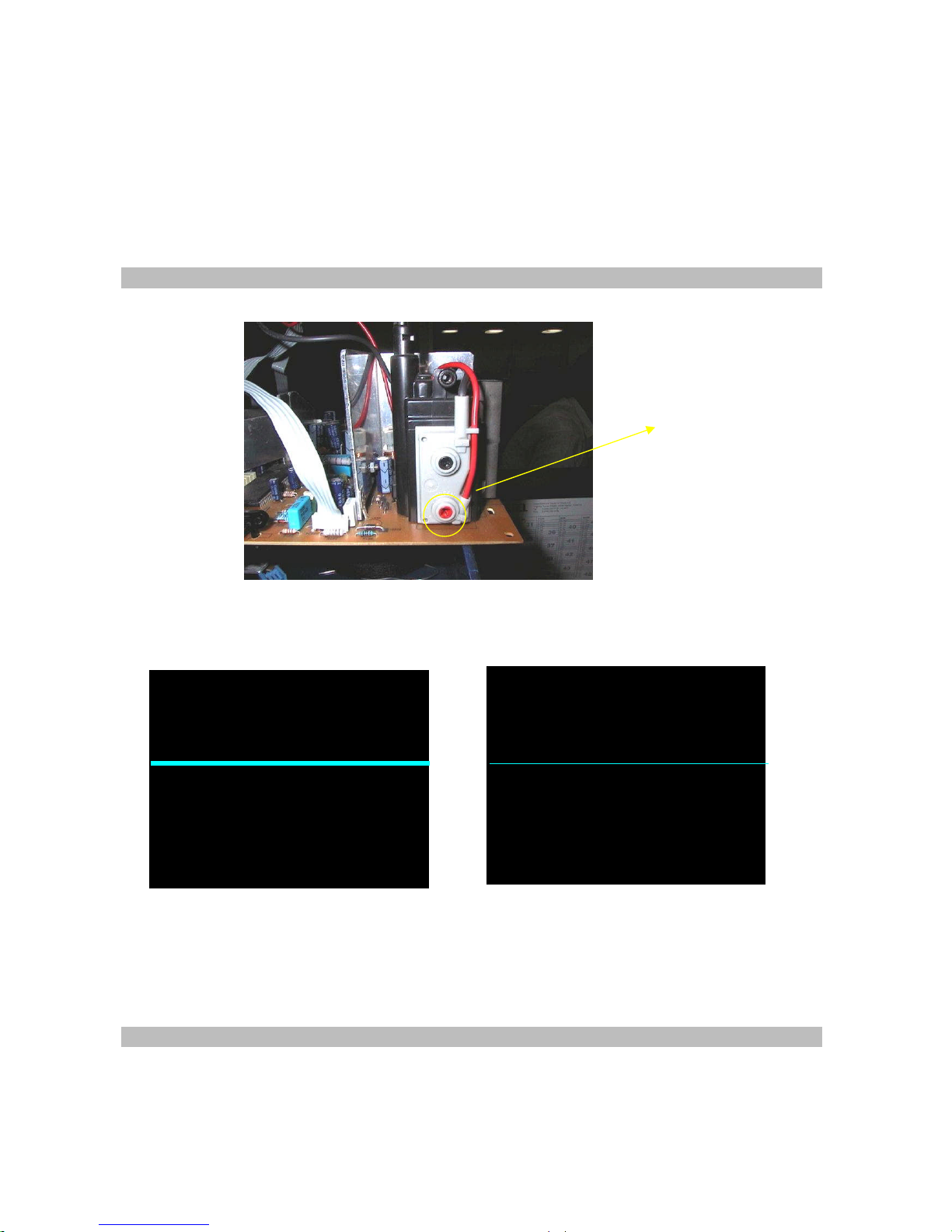
SCREEN ADJUSTMENT: (FBT Screen)
Enter service menu by pressing “MENU” and “4, 7, 2, 5” or press the mute and info buttons at the
same time from remote controller. Then press yellow button to disable vertical scan. Adjust
horizontal line via screen pot. as thin as possible. Press yellow button again to enable vertical scan.
Press “TV” button to leave service menu.
VLIN: Vertical Linearity
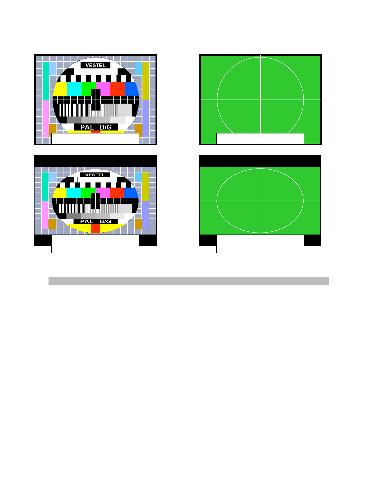
Enter a PAL B/G circle test pattern via RF. Change VLIN till you see circle as round as possible.
SCREEN
ADJ.POT.

23
Min. Value: 000
Max. Value: 063
Recommended Value : 035
RGBH: RGB Mode Horizontal Shift Offset
Enter a RGB circle test pattern via video inputs. Force the TV to RGB mode by pressing AV
button from remote controller. Change RGB Horizontal Position till the picture is horizontally
centered. Check and readjust RGBH item if the adjustment becomes improper after some other
geometric adjustments are done.
Min. Value: 000
Max. Value: 063
Default Value : 007
VSOF: Vertical Size Offset for 60 Hz
Enter an NTSC-M circle test pattern via RF or video inputs. Change Vertical Size until the
checkered parts of test pattern on both of upper and lower side disappear. Check and readjust
Vertical Size item if the adjustment becomes improper after some other geometric adjustments are
done.
Min. Value: -08
Max. Value: +55
Recommended Value: -16
VPOF: Vertical Position Offset for 60 Hz
Enter an NTSC-M circle test pattern via RF or video inputs. Change Vertical Position till the
picture is vertically centered. Check and readjust Vertical Size item if the adjustment becomes
improper after some other geometric adjustments are done.
Min. Value: -08
Max. Value: +55
Recommended Value: +09
HSOF: Horizontal Size Offset for 60 Hz
Not Used For This Model

24
HPOF: Horizontal Position Offset for 60 Hz
Enter an NTSC-M circle test pattern via RF or video inputs. Change Horizontal Position till the
picture is horizontally centered. Check and readjust Horizontal Position item if the adjustment
becomes improper after some other geometric adjustments are done.
Min. Value: -08
Max. Value: +55
Recommended Value : -06
HTOF: Horizontal Trapezoid Offset for 60 Hz
Not Used For This Model.
GEOMETRY MENU
From the service menu by pressing the green button, geometry menu appears.
To select geometry adjust parameters, use or buttons. To change the selected parameter, use
or buttons. Selected parameter will be highlighted.
Entire geometry menu parameters of AK30 CHASSIS are listed below.
VSIZ: Vertical Size for 50 Hz
Enter a PAL B/G circle test pattern via RF. Change VSIZ (Vertical Size) until horizontal black
lines on both the upper and lower part of the test pattern become very close to the upper and lower
horizontal sides of picture tube and nearly about to disappear. Check and readjust Vertical Size
item if the adjustment becomes improper after some other geometric adjustments are done.
Min. Value: 000
Max. Value: 063
Recommended Value for 4:3 mode 030
Recommended Value for 16:9 mode 063
VPOS: Vertical Position for 50 Hz
Enter a PAL B/G circle test pattern via RF. Change Vertical Position till the test pattern is
vertically centered. Horizontal line at the center pattern is in equal distance both to upper and
lower side of the picture tube. Check and readjust Vertical Position item if the adjustment becomes
improper after some other geometric adjustments are done.

25
Min. Value: 000
Max. Value: 063
Recommended Value for 4:3 mode 014
Recommended Value for 16:9 mode 020
VSCO: Vertical S-Correction for 50 Hz
Not Used For This Model.
VCCO: Vertical Corner Correction for 50 Hz
Not Used For This Model.
HSIZ: Horizontal Size for 50 Hz
Not Used For This Model.
HPOS: Horizontal Position for 50 Hz
Enter a PAL B/G circle test pattern via RF. Change Horizontal Position until the picture is
horizontally centered. Check and readjust Horizontal Position item if the adjustment becomes
improper after some other geometric adjustments are done.
Min. Value: 000
Max. Value: 063
Recommended Value for 4:3 mode 032
Recommended Value for 16:9 mode 033
HPIN: Horizontal Pincushion for 50 Hz
Not Used For This Model.
HCCO: Horizontal Corner Correction for 50 Hz
Not Used For This Model.
HTRP: Horizontal Trapezoid for 50 Hz
Not Used For This Model.
VZSZ: Vertical Zoom Size for 50 Hz
Not Used For This Model.
26
WHITE BALANCE ADJUSTMENT
The following three parameters are used to make white balance adjustment. To do this, use a
Colour Analyzer. Using WR (White point adjust for RED), WG (White point adjust for GREEN),
WB (White point adjust for BLUE) parameters, insert the + sign in the square which is in the
middle of the screen.
WR: White Point Adjustment for RED
Use this parameter to set the strength of RED in White.
Min. Value: 000
Max. Value: 063
Default Value : 030
WG: White Point Adjustment for GREEN
Use this parameter to set the strength of GREEN in White.
Min. Value: 000
50 HZ. 4:3 GEOMETRY ADJ.
50 HZ. 16:9 GEOMETRY
ADJ.
60 HZ. 4:3 GEOMETRY ADJ.

27
Max. Value: 063
Default Value : 018
WB: White Point Adjustment for BLUE
Use this parameter to set the strength of BLUE in White.
Min. Value: 000
Max. Value: 063
Default Value : 020
BR: Bias for RED
Use this parameter to set the strength of RED in BLACK.
Min. Value: 000
Max. Value: 063
Default Value : 031
BG: Bias for GREEN
Use this parameter to set the strength of GREEN in BLACK.
Min. Value: 000
Max. Value: 063
Default Value : 031
APR: Automatic RGB Peak Regulation (APR) Threshold
The goal of the APR function (Automatic RGB peak regulation) is to compensate the spread of
contrast between sources or programs by regulating the peak amplitude of RGB signals. This
results in a picture with higher contrast whatever the input signal amplitude. Besides, APR
increases the contrasts of pictures with low contrast and avoids the clipping at RGB output for
pictures with high amplitude.
To enable APR, refer to OP3 in Option Bytes.
Min. Value: 000
Max. Value: 015
Default Value : 006
The following default values are the factory settings of the corresponding items. Except Volume,
all values are restored when STANDARD button is pushed during no menu is displayed. Volume
is set to its default value only if the A.P.S. bit is set when the TV is turned on.
 Loading...