

Vertex Standard VXR-9000, VXR-9000EU Service Manual
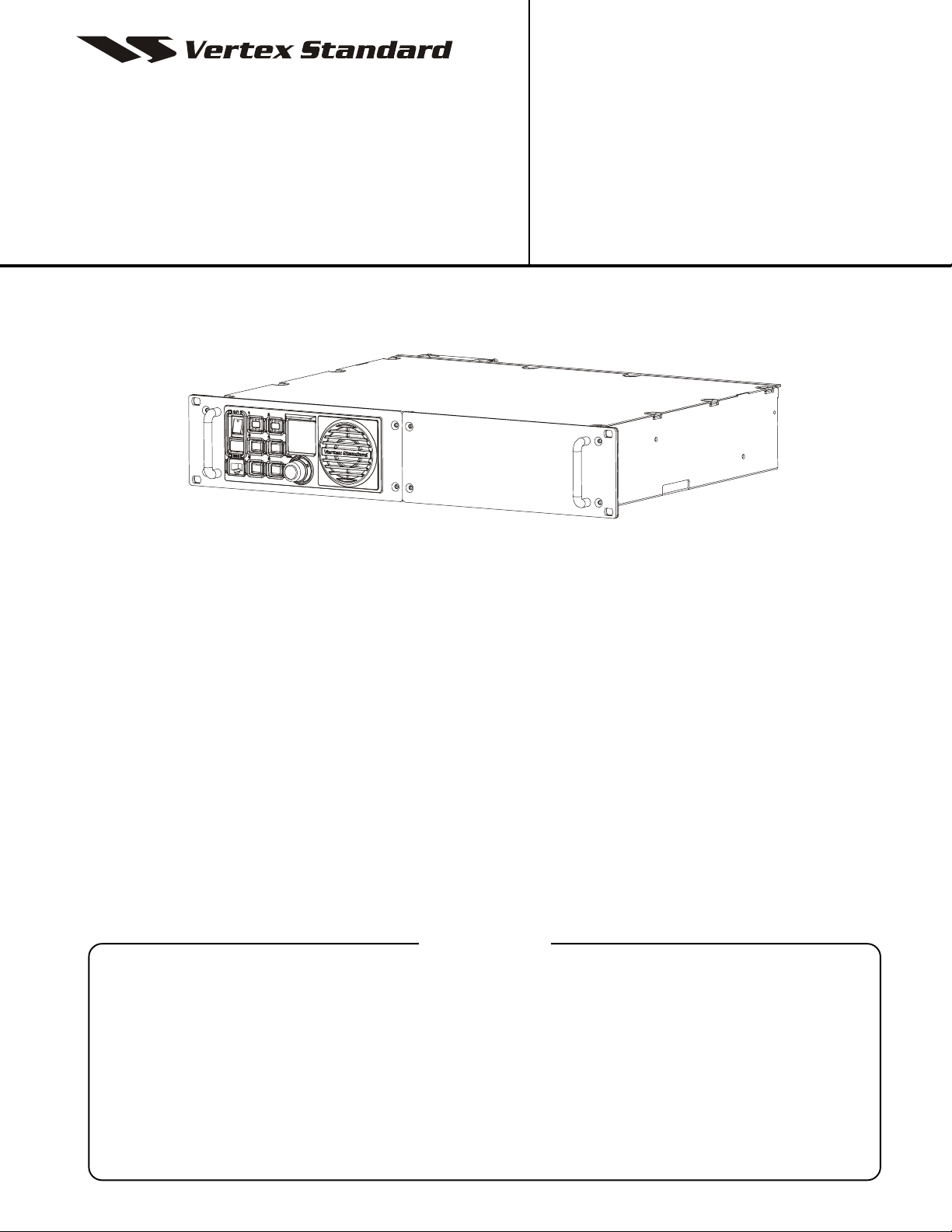
Rack Mount Repeater
VXR-9000
(
UHF
)
Service Manual
2006 VERTEX STANDARD CO., LTD. EC044U90B
©
VERTEX STANDARD CO., LTD.
4-8-8 Nakameguro, Meguro-Ku, Tokyo 153-8644, Japan
VERTEX STANDARD
US Headquarters
10900 Walker Street, Cypress, CA 90630, U.S.A.
YAESU EUROPE B.V.
P.O. Box 75525, 1118 ZN Schiphol, The Netherlands
YAESU UK LTD.
Unit 12, Sun Valley Business Park, Winnall Close
Winchester, Hampshire, SO23 0LB, U.K.
VERTEX STANDARD HK LTD.
Unit 5, 20/F., Seaview Centre, 139-141 Hoi Bun Road,
Kwun Tong, Kowloon, Hong Kong
Introduction
This manual provides the technical information necessary for servicing the VXR-9000 Rack Mount Repeater.
Servicing this equipment requires expertise in handing surface-mount chip components. Attempts by non-qualified
persons to service this equipment may result in permanent damage not covered by the warranty, and may be illegal
in some countries.
Two PCB layout diagrams are provided for each double-sided board in this transceiver. Each side of the board is
referred to by the type of the majority of components installed on that side (“Side A” or “Side B”). In most cases one
side has only chip components (surface-mount devices), and the other has either a mixture of both chip and leaded
components (trimmers, coils, electrolytic capacitors, ICs, etc.), or leaded components only.
As described in the pages to follow, the advanced microprocessor design of the VXR-9000 allows a complete alignment of this transceiver to be performed without opening the case of the radio; all adjustments can be performed from
the personal computer, using with the Vertex Standard VPL-1 Programming Cable and CE60 Software.
While we believe the information in this manual to be correct, Vertex Standard assumes no liability for damage that
may occur as a result of typographical or other errors that may be present. Your cooperation in pointing out any
inconsistencies in the technical information would be appreciated.
Contents
Specifications ........................................................... A-1
DSUB 25-pin Accessory Connector ...................... B-1
Exploded View & Miscellaneous Parts ............... C-1
Block Diagram ......................................................... D-1
Connection Diagram ............................................... E-1
Circuit Description .................................................. F-1
Alignment ................................................................ G-1
Board Units (Schematics, Layouts & Parts)
MAIN Unit .......................................................... H-1
CNTL Unit ............................................................ I-1
PANEL Unit .......................................................... J-1
PA Unit ................................................................. K-1
PA-2 Unit .............................................................. L-1
REG Unit ............................................................. M-1
SUB Unit .............................................................. N-1
100 W PA Unit (Option: Version D) .................O-1
RELAY Unit (Option) ......................................... P-1

Specifications
General
Frequency Range: A : 400 - 430 MHz, D : 450 - 490 MHz, F : 480 - 512 MHz
Number of channel:32
Channel Spacing: 5 kHz/6.25 kHz
Operating Voltage: 13.6 V DC ±10 %
Current Drain: 12 A Maximum
Duty Cycle: Receive : 100 %
Transmit : 100 % (@25 W output)
Frequency Stability: 1.5 ppm
1.0 ppm (30min after wake up)
Operating Temperature Range: –22 °F to +140 °F (–30 °C to +60 °C)
Dimensions (W x H x D): 19 x 3-1/2 x 13-1/2 inch (483 x 88 x 343 mm)
Weight (Approx.): 21.4 lbs. (9.7 kg)
Receiver
Antenna Impedance: 50 ohm
Antenna Connector: Type-BNC
Receiver Type: Double-Conversion Superheterodyne
Sensitivity: 0.35 µV (12dB SINAD), 0.45 µV (20dB Noise Quieting)
Selectivity: 83 dB (Wide), 75 dB (Narrow)
Intermodulation: 82 dB (Wide), 78 dB (Narrow)
Image Rejection: 90 dB
Squelch Threshold: –5 dBµ
Audio Output: 4 W @4 ohm
Audio Distortion:< 3 %
Hum and Noise: > 50 dB (Wide), > 45 dB (Narrow)
Audio Frequency Response: De-emphasis : 6 dB/oct (From 300 Hz to 3 kHz)
Conducted Spurious: < –80 dBm
Transmitter
RF Output Power: 50/25/10 W (High/Mid/Low)
Antenna Impedance: 50 ohm
Antenna Connector: Type-N
Modulation Type: 16K0F3E/11K0F3E
System Deviation: ±5.0 kHz (Wide), ±2.5 kHz (Narrow)
Hum and Noise: >46 dB (Wide), >43 dB (Narrow)
Microphone Sensitivity:5 mV
Audio Frequency Response: Pre-emphasis : 6dB/oct (From 300 Hz to 3 kHz)
Spurious Emission: 70 dB below carrier
Audio Distortion: 3.0 % @1 kHz
Microphone Impedance: 600 ohm
100 W PA Unit (Option)
Frequency Range: 450 - 490 MHz
Antenna Impedance: 50 ohm
Antenna Connector: Type-N
RF Output Power: 100/75/50 W (High/Mid/Low)
Duty Cycle: 100 % (@Cooling Fan “ON”)
Spurious Emission: 75 dB below carrier
Operating Voltage: 13.6 V DC ±10 %
Current Drain: 30 A Maximum
Operating Temperature Range: –22 °F to +140 °F (–30 °C to +60 °C)
Specifications subject to change without notice or obligation.
A-1

DSUB 25-pin Accessory Connector
The VXR-9000 repeater is provided with a 25-pin DB-25F
female connector for interconnections to accessories.Use
a DB-25M 25-pin male connector to connect accessories
to the repeater. The pins on the accessory connector are
explained in detail as follows:
DB-25 PIN NUMBERING
Pin 1: GND
Chassis ground for all logic levels and power supply return.
Pin 2: +13.6 V
[
POWER SUPPLY
This pin provides 13.6 Volts, 2.0 A, DC from the repeater
supply. There is a internal 3 A fuse to prevent damage to
the repeater.
]
Pin 3: TX AF IN
[
ANALOG TRANSMITTER INPUT] (VOICE BAND: 300 ~ 3,000 HZ
This pin is s audio input. Input impedance is 600 Ohms.
This audio is injected before the splatter filter stage, so
excess signal input levels are clipped.
Pin 5: TX ATT
This output is intended for controlling an external coaxial
switching relay. It is an open drain output which can sink
approx. 1.5 A when active. The delay time which is between the repeater cause to transmit mode and this port
switches to ground can be programmed by your VERTEX
STANDARD dealer.
Pin 6: DISC OUT
[
A
NALOG OUTPUT
Received signals with full system deviation produce 350
mVrms audio at this pin. The output impedance is 600
Ohm, and is extracted before the de-emphasis and squelch
circuitry. Use shielded cable to connect to this pin, and
connect the shield to GND.
] (
W
IDE-BAND: 0 ~ 3,000 HZ
)
Pin 7: N.C.
No connection.
Pin 8: RSSI
[
ANALOG OUTPUT]
A DC voltage proportional to the strength of the signal
currently being received (Receiver Signal Strength Indi-
cator) is provided on this pin. This low impedance output is generated by the receiver IF sub-system and buffered by an internal op-amp. Typical voltages are graphed
as follows:
(DC V)
e
2.5
g
a
t
l
2.0
o
V
t
u
1.5
p
t
u
1.0
O
I
S
0.5
)
S
R
0
–60 –100 –110 –120 (dBm)–70 –80 –90
Input Signal Level
Use shielded cable to connect to this pin, and connect the
shield to GND.
Pin 4: TONE IN
[
TRANSMITTER INPUT] (SUB-AUDIBLE BAND: 5 ~ 250 HZ
This pin is sub-audible tone produces 10% of full system
deviation. The nominal input voltage is 77.5 mVrms. The
input impedance is@600 Ohms, and has a flat response
characteristic (repeater deviation is constant for a given
signal level over the frequency range of 5 ~ 250 Hz). Injecting too high a voltage here causes over-deviation of
CTCSS or DCS, degrading performance. Use shielded
cable to connect to this pin, connecting the shield to GND.
)
Pin 9: COAX. SW
[
LOGIC OUTPUT (ACTIVE LOW
This output is intended for controlling an external coaxial
switching relay. It is an open drain output which can sink
approx. 1.5 A when active. This signal only switches if the
repeater has been programmed for “SIMPLEX” mode. If
programmed for “DUPLEX,” the signal remains open
(high impedance) at all time.
)]
B-1
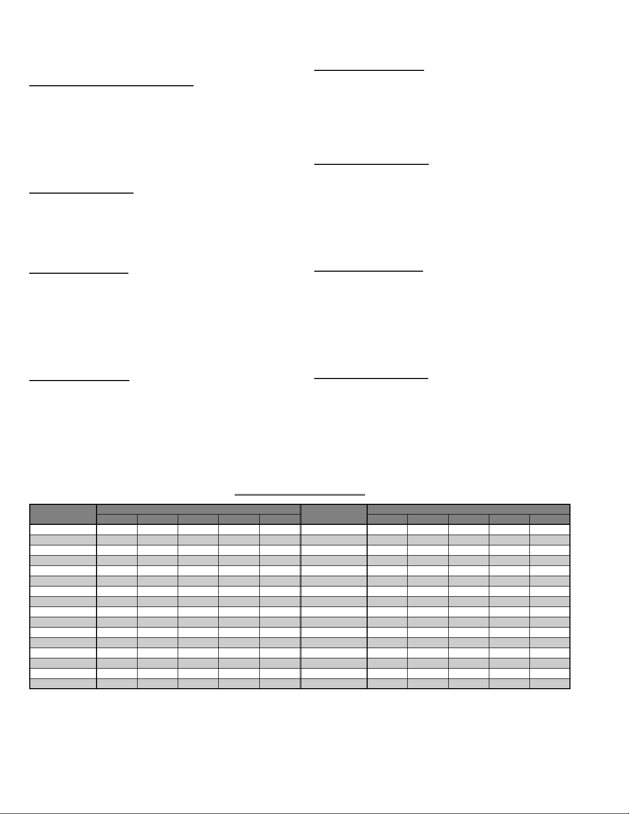
DSUB 25-pin Accessory Connector
Pin 10, 13, 15, 16, 17, 18, 19, 21:
PROGRAMMABLE I/O “0” ~ ”7”
The VXR-9000 provides eight ports (PIO) that can be programmed for various input or output signals, or for control functions. Each port may be programmed as to its
function, its status (input or output), and its logic (for output ports only). See Tables on the next page for detail regarding the input and output signals.
Pin 11: NSQ DET
This is an open-collector, active-low output capable of
sinking about 10 mA. It indicates that the receiver squelch
is open. If the squelch control is properly set, this indicates a carrier on the receiver channel.
Pin 12: EXT PTT
This input is internally pulled up to 5 VDC. When pulled
low by an external device, it keys the repeater transmitter
while the repeater is operating in the “Remote” mode.
Avoid voltage in excess of 5 V on this pin, or internal damage to the microprocessor on the repeater CNTL Unit may
result.
Pin 22: RXD LOW
[
ANALOG OUTPUT FOR DATA COMMUNICATIONS
(
300 ~ 3,000 Hz
)
This pin is an output for low speed receiving data signals
(typically 1200 bps), with the data being extracted after
the de-emphasis and low pass filter stages.
]
Pin 23: RXD HIGH
[
DIGITAL OUTPUT FOR DATA COMMUNICATIONS
(
Max.: 5 kHz
)
This pin is an output for high speed receiving data signals (typically 9600 bps), with the data being extracted
immediately after the discriminator (prior to any de-emphasis).
]
Pin 24: TXD LOW
[
NALOG INPUT FOR DATA COMMUNICATIONS
A
(
300 ~ 3,000 Hz
)
This pin is intended to be used as a low speed data signal
input to the repeater (typically 1200 bps). This digital data
signal is injected before the transmitter pre-emphasis and
limiting stages, so excess signal input levels are clipped.
]
Pin 14, 20: GND
Chassis ground for all logic levels and power supply return.
CHANNEL STEERING CHART
OPERATING
CHANNEL
1
2
3
4
5
6
7
8
9
10
11
12
13
14
15
16
4
1
1
1
1
1
1
1
1
1
1
1
1
1
1
1
1
Bin CH
3
1
1
1
1
1
1
1
1
0
0
0
0
0
0
0
0
2
1
1
1
1
0
0
0
0
1
1
1
1
0
0
0
0
1
1
1
0
0
1
1
0
0
1
1
0
0
1
1
0
0
Pin 25: TXD HIGH
[
DIGITAL INPUT FOR THE DATA COMMUNICATIONS
(
0 ~ 5 kHz
)
This pin is intended to be used as a high speed digital
data signal input to the repeater (typically 9600 bps). This
digital data signal is injected after the transmitter splatter
filter stage.
0
1
0
1
0
1
0
1
0
1
0
1
0
1
0
1
0
OPERATING
CHANNEL
17
18
19
20
21
22
23
24
25
26
27
28
29
30
31
32
4
0
0
0
0
0
0
0
0
0
0
0
0
0
0
0
0
Bin CH
3
1
1
1
1
1
1
1
1
0
0
0
0
0
0
0
0
2
1
1
1
1
0
0
0
0
1
1
1
1
0
0
0
0
]
1
1
1
0
0
1
1
0
0
1
1
0
0
1
1
0
0
0
1
0
1
0
1
0
1
0
1
0
1
0
1
0
1
0
B-2
DSUB 25-pin Accessory Connector
PROGRAMMABLE I/O PORT INPUT ITEMS
Item
Bin_CH_0
Bin_CH_1
Bin_CH_2
Bin_CH_3
Bin_CH_4
Channel_Down
Channel_Up
Compander_On
Compander_Off
Compander_Toggle
CTCSS/DCS
CTCSS/DCS
CTCSS/CS
CTCSS/DCS
CTCSS/DCS
CTCSS/CS
Two_Tone_Dec_On
Two_Tone_Dec_Off
Two_Tone_Dec_Toggle
CW_ID_On
CW_ID_Off
CW_ID_Toggle
CW_ID_Single
CW_Message_1
CW_Message_2
CW_Message_3
CW_Message_4
CW_Message_5
CW_Message_6
CW_Message_7
CW_Message_8
CW_Message_Bin_0
CW_Message_Bin_1
CW_Message_Bin_2
CW_Message_Bin_Trig
DC_Power_Save_On
DC_Power_Save_Off
DC_Power_Save_Toggle
Encryption_On
Encryption_Off
Encryption_Toggle
Encryption_Code
Local_PTT_On
Local_PTT_Off
Local_PTT_Toggle
_
Enc_On
_
Enc_Off
_
Enc_Toggle
_
Dec_On
_
Dec_Off
_
Dec_Toggle
Function
Recall the Memory Channel (Binary LSB)
Recall the Memory Channel (Binary)
Recall the Memory Channel (Binary)
Recall the Memory Channel (Binary)
Recall the Memory Channel (Binary MSB)
Step to the next-lower Operating Channel
Step to the next-higher Operating Channel
Turn the Compander Circuit "On"
Turn the Compander Circuit "Off"
Turn the Compander Circuit "On" or "Off" (Toggle)
Turn the CTCSS/DCS Encoder "On"
Turn the CTCSS/DCS Encoder "Off"
Turn the CTCSS/DCS Encoder "On" or "Off" (Toggle)
Turn the CTCSS/DCS Decoder "On"
Turn the CTCSS/DCS Decoder "Off"
Turn the CTCSS/DCS Decoder "On" or "Off" (Toggle)
Turn the 2-Tone Decoder "On"
Turn the 2-Tone Decoder "Off"
Turn the 2-Tone Decoder "On" or "Off" (Toggle)
Turn the CW IDer "On"
Turn the CW IDer "Off"
Turn the CW IDer "On" or "Off" (Toggle)
Transmit the CW ID
Send the CW Message 1
Send the CW Message 2
Send the CW Message 3
Send the CW Message 4
Send the CW Message 5
Send the CW Message 6
Send the CW Message 7
Send the CW Message 8
CW Message Recall (Binary LSB)
CW Message Recall (Binary)
CW Message Recall (Binary MSB)
Send the CW Message which is recalled from I/O port
Turn the DC Power Save Feature "On"
Turn the DC Power Save Feature "Off"
Turn the DC Power Save Featuer "On" or "Off" (Toggle)
Turn the Encryption Circuit "On"
Turn the Encryption Circuit "Off"
Turn the Encryption Circuit "On" or "Off" (Toggle)
Select the Encryption Code
Enable the Local PTT Switch
Disable the Local PTT Switch
Enable/Disable the Local PTT Switch (Toggle)
Item
Monitor_On
Monitor_Off
Monitor_Toggle
Monitor_M
Multi_Tone_Main
Multi_Tone_Sub
Multi_Tone_Toggle
Panel_Indicator_On
Panel_Indicator_Off
Panel_Indicator_Toggle
Repeat_On
Repeat_Off
Repeat_Toggle
Reset
Scan_On
Scan_Off
Scan_Toggle
Squelch_On
Squelch_Off
Squelch_Toggle
Test_Tone_On
Test_Tone_Off
Test_Tone_Toggle
Test_Tone_M
TOT_On
TOT_Off
TOT_Toggle
Transmit_On
Transmit_Off
Transmit_Toggle
TX_Power_Mid_On
TX_Power_Mid_Off
TX_Power_Mid_Toggle
TX_Power_Low_On
TX_Power_Low_Off
TX_Power_Low_Toggle
Function
Turn the Monitor Function "On"
Turn the Monitor Function "Off"
Turn the Monitor Function "On" or "Off" (Toggle)
Turn the Monitor Function "On" when the I/O port is
"High"
Select the Tone Table to "Main"
Select the Tone Table to "Sub"
Switch the Tone Table between "Main" and "Sub"
(Toggle)
Turn the Front Panel's Illumination "On"
Turn the Front Panel's Illumination Off
Turn the Front Panel's Illumination "On" or "Off" (Toggle)
Set theOperating Mode to "Repeat" mode
Set theOperating Mode to "Base" mode
Toggle theOperating Mode between the "Repeat"
mode and "Base" mode
Reset the Repeater
Start Scanning
Stop Scanning
Toggle the Scanner between "Start" and "Stop"
Turn the Squelch Circuit "On (Close)"
Turn the Squelch Circuit "Off (Close)"
Turn the Squelch Circuit "On" or "Off" (Toggle)
Generate the Test Tone Signal
Stop the generation of the Test Tone
Toggle the Test Tone genetation "On" and "Off"
Generate the Test Tone Signal when the I/O port is
"High"
Turn the Time-Out Timer featuer "On"
Turn the Time-Out Timer featuer "Off"
Turn the Time-Out Timer featuer "On" or "Off"
Enable the transmission of the Repeater
Disable the transmission of the Repeater
Enable/Disable the transmission of the Repeater
Set the transmitter power to the "Mid" level
Return the transmitter power to "Original" power level
Toggle the transmitter power between the "Mid" level
and "Original" power level
Set the transmitter power to the "Low" level
Return the transmitter power to "Original" power level
Toggle the transmitter power between the "Low" level
and "Original" power level
Item
Remote_Enb
Busy
CTCSS_Correspond
DCS_Correspond
CTCSS/
DCS_Correspond
RX_Unlock
TX_Unlock
PLL_Unlock
PROGRAMMABLE I/O PORT OUTPUT ITEMS
Function
Output the signal when the Operating mode is set to
"Repeat" mode.
Output the signal when the squelch is opened.
Output the signal when the receiving CTCSS tone is
matched.
Output the signal when the receiving DCS code is
matched.
Output the signal when the receiving CTCSS tone or
DCS code is matched.
Output the signal when the RX PLL Circuit is Unlocked.
Output the signal when the TX PLL Circuit is Unlocked.
Output the signal when the TX or RX PLL Circuit is
Unlocked.
Item
Power_Supply_Backup
Power_Supply_Voltage
Transmit
Fan_Alarm
Fan_Status
High_Temperature
TX_PD_Det
Anser_Back
Function
Output the signal when the backup power source is
used.
Output the signal when the main power source is
used.
Output the signal when the repeater is transmitting.
Output the signal when the Coolig Fan is disabled.
Output the signal when the Coolig Fan is activated.
Output the signal when the PA Unit is High Temperature.
Output the signal when the TX power is abnormalily.
Output the signal when the repeater status is
changed from the Remote Control command.
B-3

DSUB 25-pin Accessory Connector
Note:
B-4
H
FOPAJKNMG
C
B
A
D
C
F
E
G
H
I
D
EJILLMNPO
K
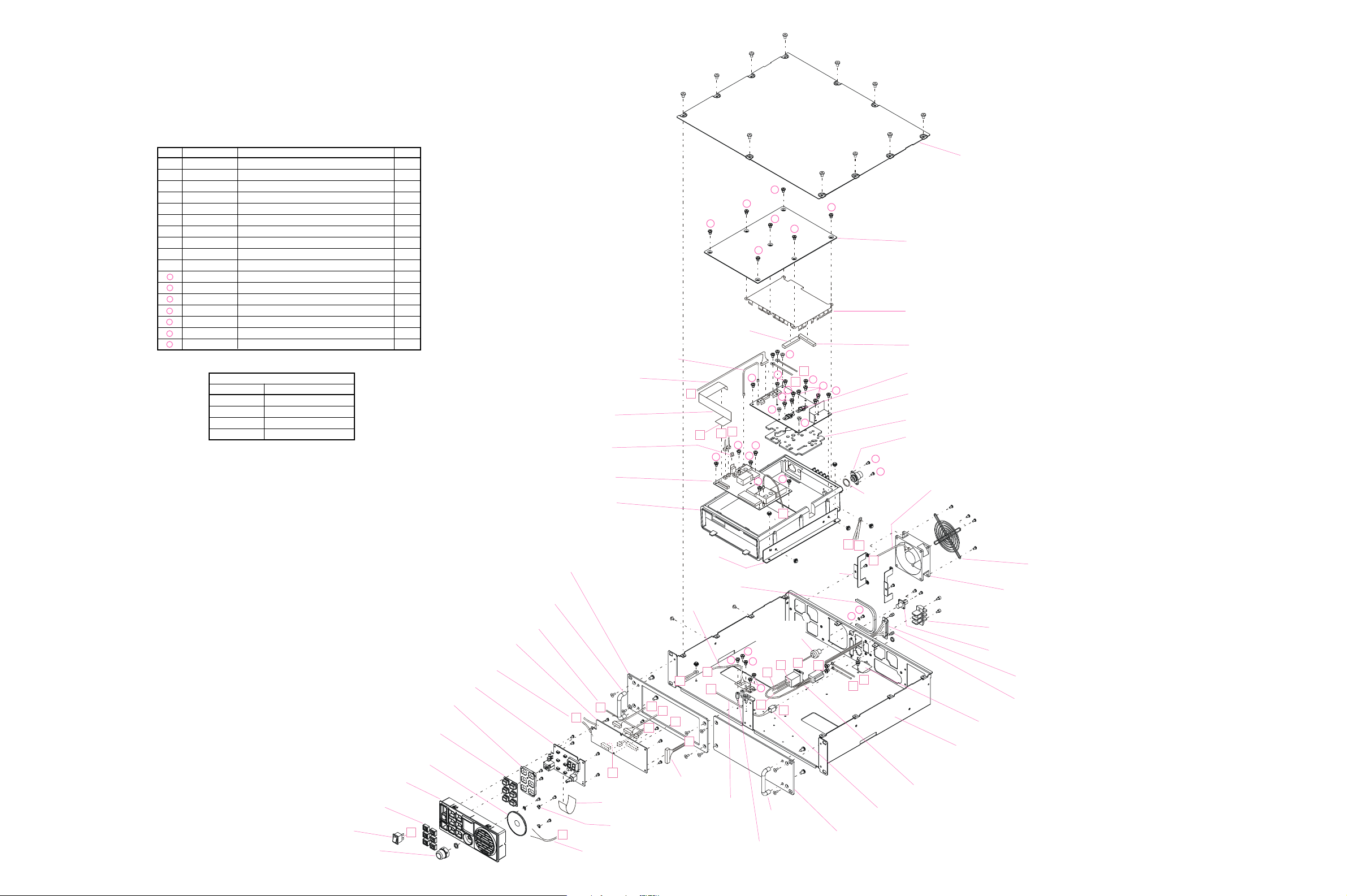
Exploded View & Miscellaneous Parts
16
16
S5000236
WASHER
RA0505300
TOP CASE
RA03328A0
CASE
RA0332900
SHIELD CASE COVER
RA0517900
GASKET
RA0506300 (2 pcs)
PLATE
PA UNIT
RA0506100
HEATSINK PLATE
P1090547
CONNECTOR
T9207039
WIRE ASSY
REF.
11
12
13
14
15
16
17
VXSTD P/N
U00508001
U30408007
U51416007
U20208002
U20406002
U20410002
U04408001
U24206001
U23308001
U04306002
U20305002
U24308001
U24310001
U52408002
U72004002
U20308002
U04408001
VXSTD P/N
Q0000075
T9023499
RA0508500
RA0506900
PAN HEAD SCREW M5X8
FLAT HEAD SCREW M4X8B
HEXA SOCKET BOLT M4X16B
BINDING HEAD SCREW M2.6X8NI
BINDING HEAD SCREW M4X6NI
BINDING HEAD SCREW M4X10NI
SEMS SCREW HSM4X8
TAPTITE SCREW M2.6X6
TAPTITE SCREW M3X8
SEMS SCREW HSM3X6NI
BINDING HEAD SCREW M3X5NI
TAPTITE SCREW M3X8
TAPTITE SCREW M3X10
HEX HEAD BOLT M4X8NI
TOOTHED LOCK WASHER OW4NI
BINDING HEAD SCREW M3X8NI
SEMS SCREW HSM4X8
ACCESSORIES
DESCRIPTION
DESCRIPTION
BLADE FUSE
DC CABLE
NAME PLATE
KNOB CAP
Non-designated parts are available only as
part of a designated assembly.
QTY.
4
8
2
2
14
4
7
3
12
2
12
13
8
1
1
2
1
T9207037A
WIRE ASSY
T9207049
WIRE ASSY
R0134490
HOLDER
MAIN UNIT
RA050140A
CHASSIS
T9318202
WIRE ASSY
11
RA0530900
GASKET
12
12
11
12
11
11
11
11
11
12
13
12
12
12
12
12
13
13
12
12
12
12
RA0505900
RA0506000
PAN EL
S5000241
HANDLE
T9207032
WIRE ASSY
CNTL UNIT
T9318204
WIRE ASSY
PANEL UNIT
RA0507000
RA0506800
RA0506900 (6 pcs)
KNOB CAP (ACCESSORIES)
N2090061
ROCKER SWITCH
RA0510000
FRONT PANEL ASSY
RA02543A0
KNOB
RUBBER KNOB
PLATE
M4090150
SPEAKER
T9206754
WIRE ASSY
T9207034A
WIRE ASSY
R0145680 (3 pcs)
HOLDER
BRACKET
S0000074
RUBBER GROMMET
T9207048
WIRE ASSY
T9207047
WIRE ASSY
T9207046
WIRE ASSY
T9207053
WIRE ASSY
11
11
11
11
S5000223 (3 pcs)
SPACER
RA0506500 (2 pcs)
MOTOR HOLDER
S5000241
HANDLE
14
15
RA0505500
PAN EL
T9207055
WIRE ASSY
P1090654
CONNECTOR
S5000242
FINGER GUARD
M2090037
FAN
Q6000170
TERMINAL STRIP
P1091181
CONNECTOR
P1091072
CONNECTOR
S5000182
SCREW
RA0506600
COVER
RA0505400
BASE
RA0532800
LABELREAR
C-1

Exploded View & Miscellaneous Parts
Note
C-2
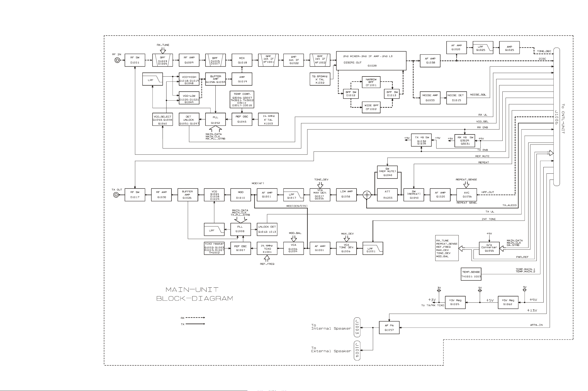
Block Diagam
MAIN Unit
D-1
Block Diagam
CNTL Unit, PANEL Unit, & PA Unit
D-2
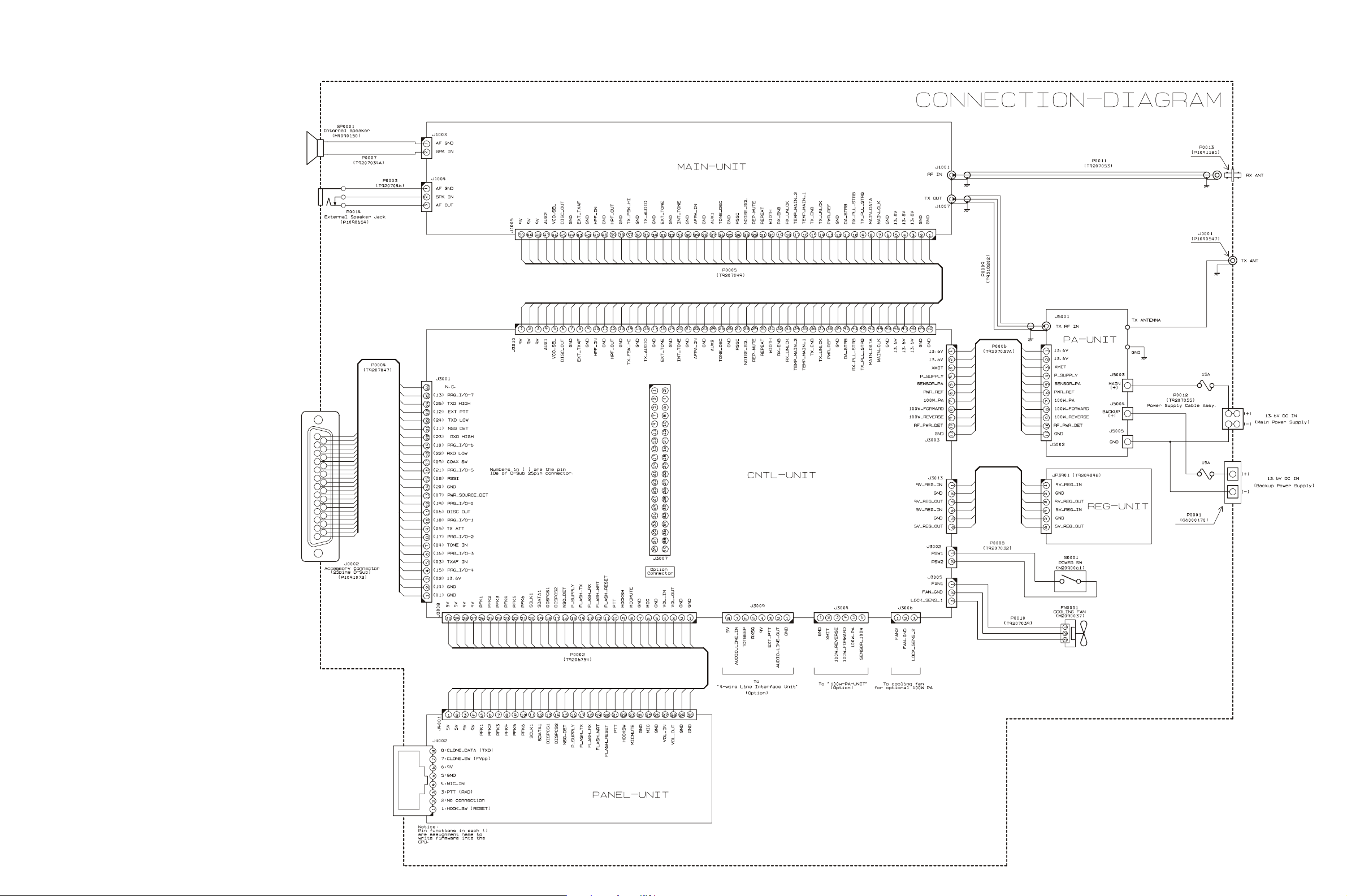
Connection Diagam
E-1
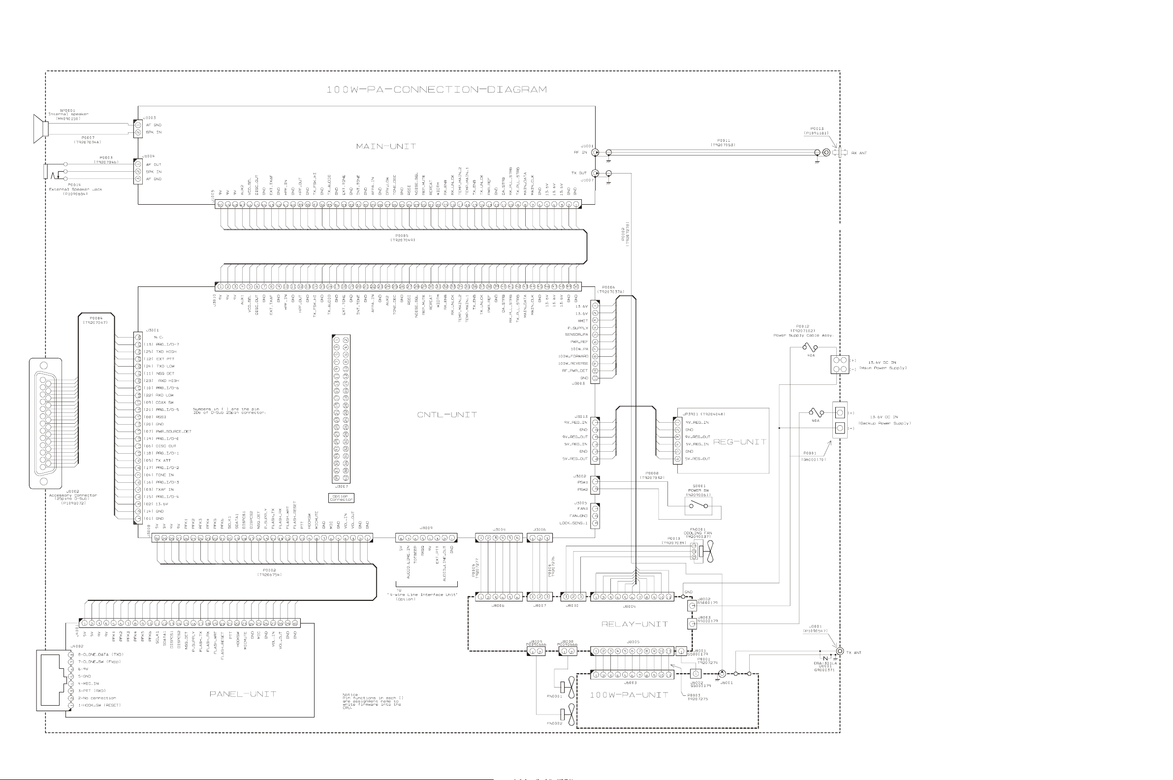
Connection Diagam (with Optional 100 W PA Unit)
E-2

Circuit Description
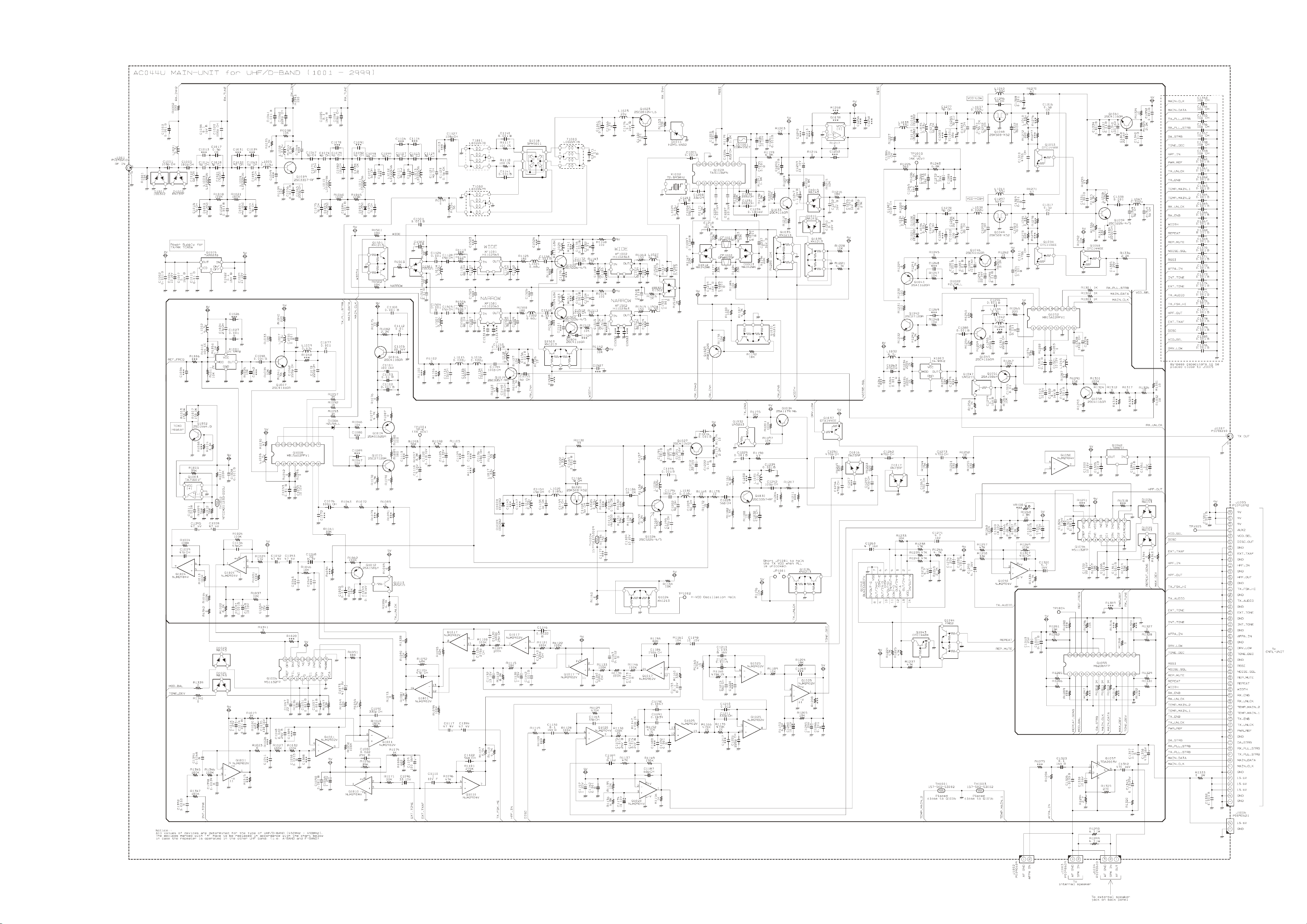
RECEIVE SIGNAL PATH
Incoming RF from the RX antenna jack is delivered to the
MAIN Unit and passes through the protection diode
D1001 (1SS302) and a varactor-tuned band pass filter con-
sisting of coils L1003 and L1004, capacitors C1015, C1018,
C1021, C1032, and C1044, and diodes D1003 and D1004
(both HVU350). Signals are then applied to the RF amplifier, Q1009 (2SC3357). The amplified RF signal is applied
through a varactor-tuned band pass filter consisting of
coils L1010 and L1011, capacitors C1079, C1092, C1082,
C1095 and C1075, and diodes D1007 and D1005 (both
HVU350) to the first mixer Q1018 (SPM5001) along with
the first local signal from the PLL circuit.
The first local signal is generated between 376.65 MHz
and 416.65 MHz by the RX VCO, which consists of FET
Q1048 (2SK508) and varactor diodes D1018 and D1019
(both 1SV282) or FET Q1049 (2SK508) and varactor diodes D1020 and D1021 (both 1SV282), according to the
programmed receiving frequency; the local signal then
passes through buffer amplifier Q1059 (2SC5226) and
first local amplifier Q1019 (2SC3357) to the first mixer
Q1018 (SPM5001).
The 73.35 MHz first IF signal is applied to monolithic crystal filters XF1001 and XF1002 which strip away unwanted mixer products, and the IF signal is applied to the first
IF amplifiers Q1022 (2SC5226). The amplified first IF sig-
nal is then delivered to the FM IF subsystem IC Q1028
(TA31136FN), which contains the second mixer, second
local oscillator, limiter amplifier, noise amplifier, and FM
detector.
The second local oscillator signal, generated by the 72.895
MHz crystal X1002, produces the 455 kHz second IF signal when mixed with the first IF signal within Q1028
(TA31136FN). The second IF signal passes through ceramic filter CF1001 or CF1002 which strips away all but
the desired signal, and then passes through the limiter
amplifier within Q1028 (TA31136FN) to ceramic discrim-
inator CD1001, which removes any amplitude variations
in the 455 kHz IF signal before detection of speech. The
detected audio passes through the low pass filter, consisting of R1199 and C1244, which rejects the 455 kHz IF
component.
The audio signal from the MAIN Unit is delivered to the
CNTL Unit and passes through the audio amplifier Q1020
(NJM2904V) to the active high pass filter section of Q3020
(FX805LG), which rejects the sub-audible frequency component. The filtered audio signal is delivered to electronic volume Q1056, which adjusts the audio sensitivity to
compensate for audio level variations, then passes through
audio amplifier Q1020 (NJM2904V), audio switch Q1040
(BU4066BCFV), attenuator consisting of R1233, and limiter amplifier Q1050 (NJM2904V), to the electronic vol-
ume control Q1056 (M51132FP), where the maximum deviation is set. The audio signal subsequently passes
through the 3-section active low pass filter consisting of
Q1017-1/-2/-3 (NJM2902V) and audio amplifier Q1001
(NJM2902V) to providing the repeater transmit audio.
A portion of the audio signal from the active high pass
filter section of Q4024 (NJM2902V) is de-emphasized con-
sisting of Q3036 (TA75S01F), R3198, and C3144, provid-
ing a flat audio response. The filtered audio then passes
through the active band pass filter Q3021 (NJM2902V)
and audio mute gate Q3015 (DTC323TK) to audio power
amplifier Q1057 (TDA2003), providing up to 2 Watts of
audio power to the 8 Ohm loudspeaker.
SUB-AUDIBLE SIGNALING (DECODER
A portion of the audio signal from the audio amplifier
Q1020 (NJM2904V) passes through the 3-section active
low pass filter Q1025 (NJM2902V) and the low pass fil-
tering section of Q3020 (FX805LG) to separate the CTCSS tones from the received audio signal. The CTCSS tones
are sent to the CTCSS decoder section of Q3020
(FX805LG). When a CTCSS tone is received, the CTCSS
information is delivered to pin 77 of the Main CPU Q3014
(HD64F2238) from pin 4 and 8 of Q3020 (FX805LG) which
compares the CTCSS tone with the programmed tone.
Another portion of the audio signal passes through the 3section active low pass filter Q3044 (NJM2902V) to separate the DCS codes from the received audio signal. The
low pass filtered signal passes through the phase detector Q3044 (NJM2902V) to pin 39 of the Main CPU Q3014
(HD64F2238). When a DCS code is received, the Main
CPU Q3014 (HD64F2238) compares the DCS code with
the programmed code.
If the received CTCSS tone or DCS code matches the programmed tone or code, pin 4 of the Main CPU Q3014
(HD64F2238) goes low, turning off the squelch switch
Q3015 (DTC323TK) and passing the received audio sig-
nal to the audio power amplifier Q1057 (TDA2003V).
)
SQUELCH CONTROL
The squelch circuit consists of noise amplifier Q1033
(2SC4116GR) and noise detector D1015 (MA143) on the
MAIN Unit, and control circuitry within Main CPU Q3014
(HD64F2238) on the CNTL Unit.
When no carrier is received, noise at the output of the audio detector stage of Q1028 (TA31136FN) is amplified by
Q1033 (2SC4116GR), and then rectified by D1015
(MA143) to provide a DC control voltage for the squelch
switch. The resulting DC voltage is delivered to pin 23 of
J1005.
The DC voltage from the MAIN Unit is delivered to the
A-D analog input port (pin 51) of the Main CPU Q3014
F-1

Circuit Description
(HD64F2238) on the CNTL Unit, which compares the
squelch threshold level to that which is memorized in EEPROM Q3006 (BR24L32F) or set by the front panel SQL
control.
RX PLL AND VCO CIRCUITS
The receiver’s PLL circuitry consists of PLL subsystem IC
Q1052 (MB15A02PFV1) on the MAIN Unit, which con-
tains a reference oscillator/divider, serial-to-parallel data
latch, programmable divider, phase comparator and a
swallow counter. Stability is obtained by a regulated 5
VDC supply via Q1062 (L78M05T) and temperature com-
pensated 14.4 MHz crystal oscillator X1003.
The RX VCO made up two VCO circuit, one is Low-Band
RX VCO, consisting of FET Q1048 (2SK508) and varactor
diodes D1018 and D1019 (both 1SV282), and another one
is High-Band RX VCO, consisting of FET Q1049 (2SK508)
and varactor diodes D1020 and D1021 (both 1SV282), oscillates between 376.65 MHz and 416.65 MHz according to
the programmed receiving frequency. The RX VCO output passes through buffer amplifier Q1059 (2SC5226) and
first local amplifier Q1019 (2SC3357) to the first mixer
Q1018 (SPM5001), as described previously. A portion of
the RX VCO output is applied to the prescaler/swallow
counter section in the PLL IC Q1052 (MB15A02PFV1).
There the RX VCO signal is divided by 64 or 65, according
to a control signal from the Main CPU Q3014 (HD64F2238)
on the CNTL Unit, before being applied to the programmable divider section of the PLL IC Q1052
(MB15A02PFV1).
The data latch section of the PLL IC Q1052
(MB15A02PFV1) also receives serial dividing data from
the Main CPU Q3014 (HD64F2238), which causes the predivided RX VCO signal to be further divided by 75,330 ~
81,330 (or 60,264 ~ 65,064) in the programmable divider
section in the PLL IC Q1052 (MB15A02PFV1), depend-
ing upon the desired receive frequency, so as to produce
a 5 kHz (or 6.25 kHz) derivative of the current RX VCO
frequency. Meanwhile, the reference divider section of the
PLL IC Q1052 (MB15A02PFV1) divides the 14.4 MHz
crystal reference from the reference oscillator X1003 and
Q1045 (2SC4116GR) by 2880 (or 2304) to produce the 5
kHz (or 6.25 kHz) loop reference.
The 5 kHz or 6.25 kHz signal from the programmable divider (derived from the RX VCO) and that derived from
the crystal are applied to the phase detector section of the
PLL IC Q1052 (MB15A02PFV1), which produces a pulsed
output with pulse duration depending on the phase difference between the input signals. This pulse train is then
converted to DC, low pass filtered, then fed back to the
RX VCO varactor diodes D1018/D1019 and D1020/D1021
(all 1SV282).
Changes in the DC voltage applied to the varactor diodes
D1018/D1019 and D1020/D1021 (all 1SV282) affect the
reactance in the tank circuit RX VCO Q1048/1049 (both
2SK508), changing the oscillating frequency according
to the phase difference between the signals derived from
the RX VCO and the crystal reference oscillator. The RX
VCO is thus phase-locked to the reference frequency standard.
TRANSMIT SIGNAL PATH
The speech audio from the CNTL Unit is applied to the
varactor diode D1010 (HVU350), which frequency mod-
ulates the TX VCO from the unmodulated carrier at the
transmit frequency. The modulated transmit signal is buffered by Q1026 (2SC5226), then passes through the RF
amplifier Q1030 (2SC3357) and RF diode switch D1016
(RN739F) to the PA Unit.
The transmit signal is applied to the RF amplifier Q5001
(2SC3357) and Q5008 (PD55008), then finally amplified
by power amplifier Q5015 and Q5016 (both PD55025S)
up to 50 Watts. Harmonic and spurious radiation in the
final output is suppressed by a low pass filter consisting
of coils L5007 ~ L5010, plus capacitors C5071, C5078,
C5082, C5085, and C5088 on the PA Unit, before delivery
to the TX antenna jack.
TX PLL AND VCO CIRCUITS
The Transmitter’s PLL circuitry consists of PLL subsystem
IC Q1008 (MB15A02PFV1) on the MAIN Unit, which contains a reference oscillator/divider, serial-to-parallel data
latch, programmable divider, phase comparator and a
swallow counter. Stability is obtained by a regulated 5
VDC supply via Q1062 (L78M05T) and temperature com-
pensated 14.4 MHz crystal oscillator X1001.
The TX VCO, consisting of FET Q1021 (2SK508) and var-
actor diodes D1008 and D1009 (both 1SV282), oscillates
between 450 MHz and 490 MHz according to the programmed transmit frequency. The theory of operation of
the remainder of the PLL circuitry is similar to that of the
RX PLL circuit; however, dividing data from the Main
CPU Q3014 (HD64F2238) on the CNTL Unit is such that
the VCO frequency is the actual transmit frequency.
APC (AUTOMATIC POWER CONTROL
RF power output from the final amplifier Q5015/Q5016
(both PD55025S) is sampled by C5061/C5056 and is then
rectified by D5007 and D5008 (both HSM88AS). The resulting DC voltage is applied to the comparator Q5005
(TA75S01F), where the voltage is compared with a reference voltage from the Main CPU Q3014 (HD64F2238) on
the CNTL Unit, to produce a control voltage for the Automatic Power Controller Q5004 (2SC4116GR) and
)
F-2

Q5002 (2SB1122S), which regulates supply voltage to
Q5001 (2SC3357).
)
CNTL (CONTROL
The CNTL Unit consists of 8-bit CPU Q3014 (HD64F2238),
EEPROM Q3006 (BR24L32F), RX and TX speech audio
circuits, and various analog switches for the CPU and repeater interconnections.
Microprocessor operational code is stored in Q3006
(BR24L32F), while channel data and repeater configuration information is programmed from an external PC connected to the front panel’s MIC jack via a VPL-1 programming cable.
The output from the Main CPU Q3014 (HD64F2238) con-
tains serial control data used for REPEATER/BASE mode
control, as well as TX and RX PLL data. Crystal X3002
oscillates at 12.288 MHz, and provides stable clock timing for the Main CPU. When the repeater is powered on,
the voltage at pin 62 of Q3014 (HD64F2238) becomes sta-
ble, and the output of voltage detector IC Q3012
(BD4845FVE), which is tied to pin 59 (RST) of Q3014
(HD64F2238) becomes high, resetting the Main CPU.
U
NIT
Circuit Description
BASE OPERATION (TX, MIC-INPUT AUDIO)
Microphone input is delivered past the MIC MUTE switch
Q4002 (DTC323TK), then passes through the audio am-
plifier and active high pass filter at Q4001 (NJM2902V)
when the signal is processed in the same manner as previously described.
F-3

Circuit Description
Note:
F-4

Alignment
Introduction
The VXR-9000 has been aligned at the factory for the specified performance across the entire frequency range specified. Realignment should therefore not be necessary except in the event of a component failure. All component
replacement and service should be performed only by an
authorized Vertex Standard representative, or the warranty policy may be voided.
The following procedures cover the sometimes critical and
tedious adjustments that are not normally required once
the transceiver has left the factory. However, if damage
occurs and some parts are replaced, realignment may be
required. If a sudden problem occurs during normal operation, it is likely due to component failure; realignment
should not be done until after the faulty component has
been replaced.
We recommend that servicing be performed only by authorized Vertex Standard service technicians who are experienced with the circuitry and fully equipped for repair and alignment. Therefore, if a fault is suspected, contact the dealer from whom the transceiver was purchased
for instructions regarding repair. Authorized Vertex Standard service technicians realign all circuits and make complete performance checks to ensure compliance with factory specifications after replacing any faulty components.
Those who do undertake any of the following alignments
are cautioned to proceed at their own risk. Problems
caused by unauthorized attempts at realignment are not
covered by the warranty policy. Also, Vertex Standard
must reserve the right to change circuits and alignment
procedures in the interest of improved performance, without notifying owners. Under no circumstances should any
alignment be attempted unless the normal function and
operation of the transceiver are clearly understood, the
cause of the malfunction has been clearly pinpointed and
any faulty components replaced, and the need for realignment determined to be absolutely necessary. The following test equipment (and thorough familiarity with its correct use) is necessary for complete realignment. Correction of problems caused by misalignment resulting from
use of improper test equipment is not covered under the
warranty policy. While most steps do not require all of
the equipment listed, the interactions of some adjustments
may require that more complex adjustments be performed
afterwards. Do not attempt to perform only a single step
unless it is clearly isolated electrically from all other steps.
Have all test equipment ready before beginning, and follow all of the steps in a section in the order presented.
Required Test Equipment
RF Signal Generator with calibrated output level at 1
GHz
AF Signal Generator
Frequency Counter: ±0.2 ppm accuracy at 1 GHz
In-line Wattmeter with 5% accuracy at 1 GHz
50-ohm, 50-W RF Dummy Load (50 W mode) or 50-
ohm, 100-W RF Dummy Load (100 W mode)
13.6V Regulated DC Power Supply with capable up to
15A (50 W mode) or 30A (100 W mode).
AC Voltmeter
DC Voltmeter
UHF Sampling Coupler
Microsoft® Windows® 98 or later operating system
Vertex Standard VPL-1 Connection Cable, FRB-4 Tun-
ing I/F Box, and CE60 Programming Software
Alignment Preparation & Precautions
A 50-ohm RF Dummy load and in-line wattmeter must
be connected to the main antenna jack in all procedures
that call for transmission, except where specified otherwise. Correct alignment is not possible with an antenna.
After completing one step, read the following step to determine whether the same test equipment will be required.
If not, remove the test equipment (except dummy load
and wattmeter, if connected) before proceeding.
Correct alignment requires that the ambient temperature
be the same as that of the transceiver and test equipment,
and that this temperature be held constant between 20 °C
and 30 °C (68 °F ~ 86 °F). When the transceiver is brought
into the shop from hot or cold air, it should be allowed
time to come to room temperature before alignment.
Whenever possible, alignments should be made with oscillator shields and circuit boards firmly affixed in place.
Also, the test equipment must be thoroughly warmed up
before beginning.
Note: Signal levels in dB referred to in this procedure are
based on 0 dBµ EMF = 1.0 µV.
G-1
Alignment
The Alignment Tool Outline
1. Install the CE60 (Programming Software) to your PC.
2. Execute the CE60 with the “/d” option (Dealer mode:
type “ce60win.exe /d” [ENTER]).
3. You may adjust the following parameters from the
computer.
RX Sensitivity
Squelch Sensitivity
TX Power
Maximum Deviation <Wide/Narrow>
Maximum Deviation <Wide/Narrow>
Sub-Audio (CTCSS/DCS) Deviation <Wide/Nar-
row>
Modulation Balance
Repeat Sensitivity
TX Power Down Detect
PLL Reference Frequency
RX Sensitivity
Setup the test equipment as shown below.
MIC
EXT SP
)
SINAD Meter
4-ohm
Dummy Load
RF Signal
Generator
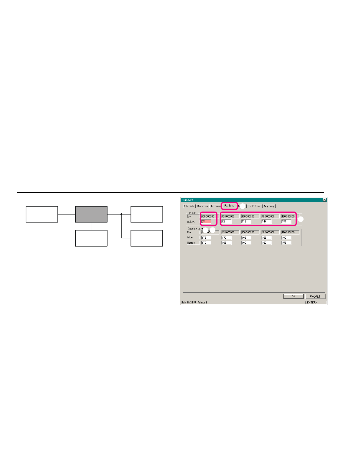
Open the “Alignment” window, then click the left
mouse button on the “Rx Tune” tab to move to the “Rx
Tune” screen.
Click the left mouse button on the “Low Band Edge
Frequency” box on the “RX BPF” field (highlighted in
“pink”).
Set the RF Signal Generator output to the “Low Band
Edge” Frequency, at a level of –6 dBµV, ±3.0 kHz deviation with a 1 kHz audio tone.
Press the [Page Up]/[Page Down] key so that the
SINAD meter reaches maximum deflection.
Repeat above steps at the other four points (box: fre-
quencies).
RX ANT
VXR-9000
Computer
(
CE60
G-2
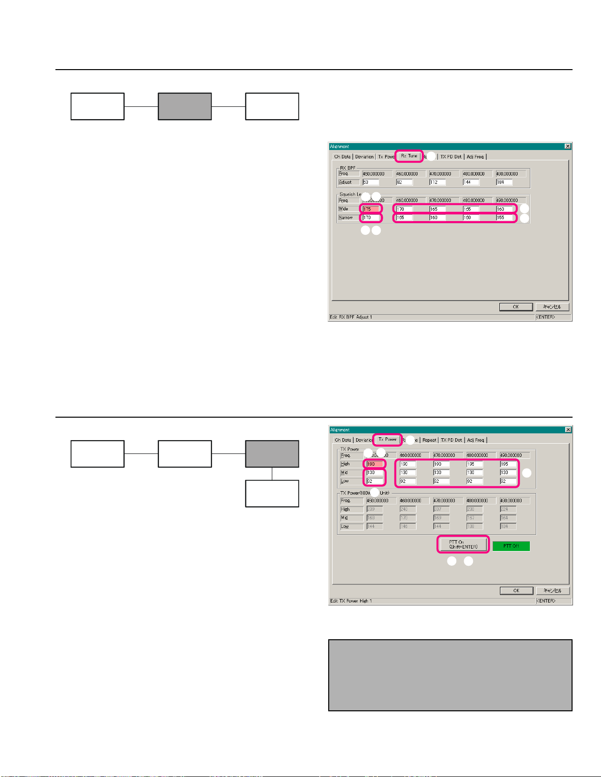
SQL Sensitivity
Alignment
Setup the test equipment as shown below.
RF Signal
Generator
Open the “Alignment” window, then click the left
mouse button on the “Rx Tune” tab to move to the “Rx
Tune” screen.
Click the left mouse button on the “Wide” box on the
“Low Band Edge Frequency” area of the “Squelch
Level” field (highlighted in “pink”).
Set the RF Signal Generator output to the “Low Band
Edge” Frequency, at a level of –3 dBµV, ±3.0 kHz deviation with a 1 kHz audio tone.
Press the [Page Down] key until the squelch close, then
press the [Page Up] key to the point where the squelch
is just opened.
Repeat above steps at the other four points (box: fre-
quencies).
Click the left mouse button on the “Narrow” box on
the “Low Band Edge Frequency” area of the “Squelch
Level” field (highlighted in “pink”).
Set the RF Signal Generator output to the “Low Band
Edge” Frequency, at a level of –3 dBµV, ±1.5 kHz deviation with a 1 kHz audio tone.
RX ANT
VXR-9000
MIC
Computer
(
CE60
Press the [Page Down] key until the squelch close, then
press the [Page Up] key to the point where the squelch
)
is just opened.
Repeat the above steps at the four points (box: frequen-
cies).
TX Power
Setup the test equipment as shown below.
50-ohm
Dummy Load
Open the “Alignment” window, then click the left
mouse button on the “Tx Power” tab to move to the
“Tx Power” screen.
Click the left mouse button on the “High” box on the
“Low Band Edge Frequency” area of the “TX Power”
field (highlighted in “pink”).
Click the left mouse button on the “PTT On” button to
actitvate the transmitter (the “PTT On” label is changed
to “PTT Off”).
Press the [Page Up]/[Page Down] key so that the
Power Meter reading is 50 W.
Click the left mouse button on the “PTT Off” button
to disable the transmitter (the “PTT Off” label is returned to “PTT On”).
Repeat the above steps at the “Mid” (25 W) and “Low”
(10 W) boxs.
Repeat the above steps at the 12 points (box: frequen-
cies).
Inline
Wattmeter
TX ANT
VXR-9000
Computer
(
CE60
MIC
)
Note: When the optional 100 PA Unit is installed, perform this adjustment parameter in the “TX Power (100
W Unit)” field. In this case, adjust the “High” power to
“100 W,” “Mid” power to “50 W,” and “Low” power to
“25 W.”
G-3
Alignment
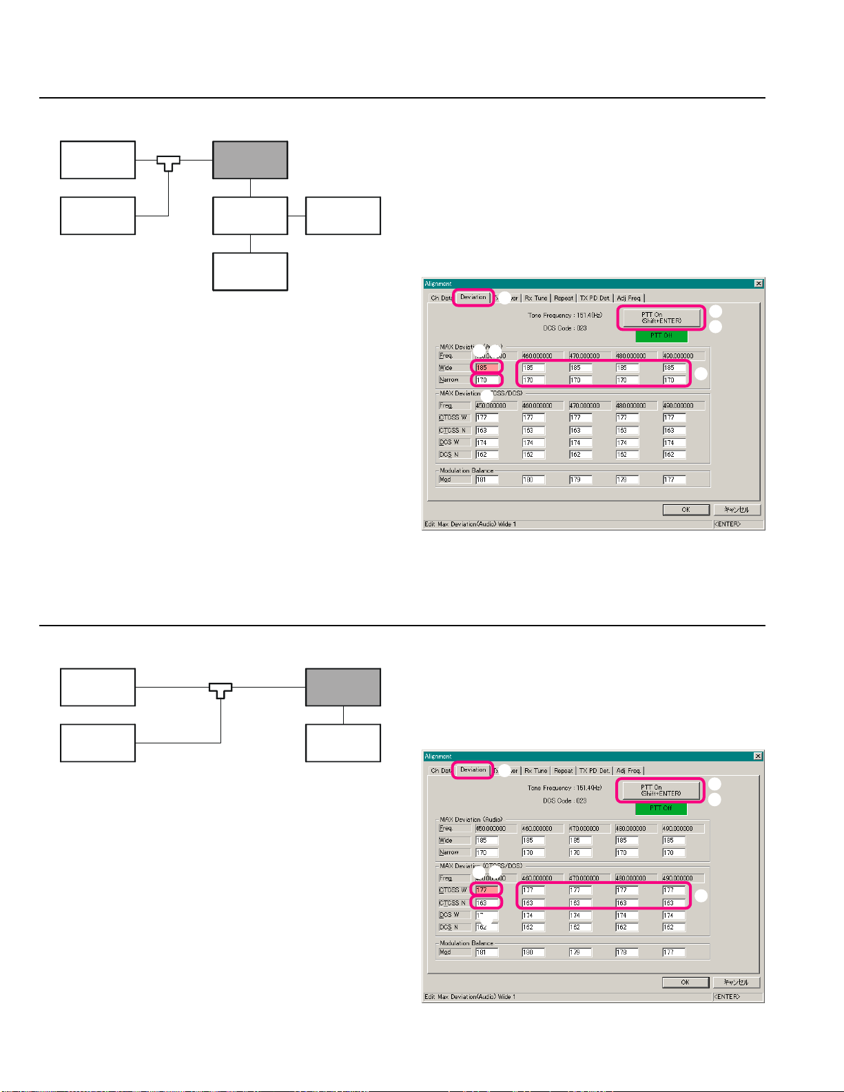
Maximum Deviation
Setup the test equipment as shown below.
Sampling
50-ohm
Dummy Load
Deviation
Meter
Set the AF Signal Generator output to 35 mVrms at 1
kHz.
Open the “Alignment” window, then click the left
mouse button on the “Deviation” tab to move to the
“Deviation” screen.
Click the left mouse button on the “Wide” box on the
“Low Band Edge Frequency” area of the “MAX Deviation (Audio)” field (highlighted in “pink”).
Click the left mouse button on the “PTT On” button to
actitvate the transmitter (the “PTT On” label is changed
to “PTT Off”).
Press the [Page Up]/[Page Down] key so that the De-
viation Meter reading is 4.2 kHz ±0.2 kHz.
Coupler
TX ANT
VXR-9000
MIC
TUNING I/F BOX
(
)
FRB-4
Computer
(
)
CE60
AF Signal
Generator
Click the left mouse button on the “PTT Off” button
to disable the transmitter (the “PTT Off” label is returned to “PTT On”).
Repeat the above steps at the “Narrow” box on the
“Low Band Edge Frequency” area of the “MAX Deviation (Audio)” field (highlighted in “pink”) so that
the Deviation Meter reading is 2.1 kHz ±0.1 kHz.
Repeat the above steps at the eight points (box: fre-
quencies).
Sub-Audio (CTCSS) Deviation
Setup the test equipment as shown below.
Sampling
50-ohm
Dummy Load
Deviation
Meter
Open the “Alignment” window, then click the left
mouse button on the “Deviation” tab to move to the
“Deviation” screen.
Click the left mouse button on the “CTCSS W” box on
the “Low Band Edge Frequency” area of the “MAX
Deviation (CTCSS/DCS)” field (highlighted in “pink”).
Click the left mouse button on the “PTT On” button to
actitvate the transmitter (the “PTT On” label is changed
to “PTT Off”).
Press the [Page Up]/[Page Down] key so that the De-
viation Meter reading is 0.75 kHz ±0.05 kHz.
Click the left mouse button on the “PTT Off” button
to disable the transmitter (the “PTT Off” label is returned to “PTT On”).
Coupler
TX ANT
VXR-9000
Computer
(
CE60
MIC
Repeat the above steps at the “CTCSS N” box on the
“Low Band Edge Frequency” area of the “MAX Deviation (CTCSS/DCS)” field (highlighted in “pink”) so
that the Deviation Meter reading is 0.38 kHz ±0.02 kHz.
Repeat the above steps at the eight points (box: fre-
quencies).
)
G-4
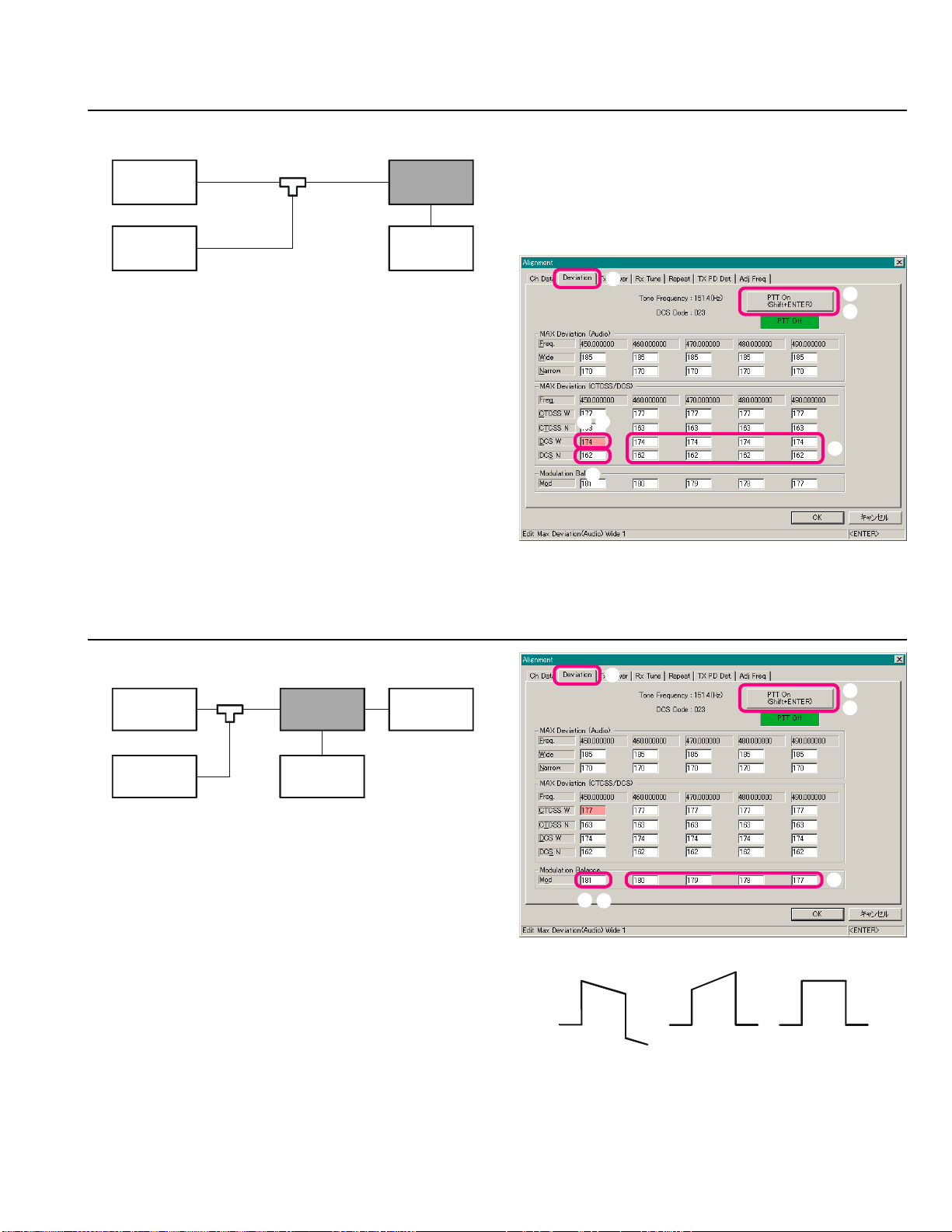
Sub-Audio (DCS) Deviation
g
Alignment
Setup the test equipment as shown below.
Samplin
50-ohm
Dummy Load
Deviation
Meter
Open the “Alignment” window, then click the left
mouse button on the “Deviation” tab to move to the
“Deviation” screen.
Click the left mouse button on the “DCS W” box on
the “Low Band Edge Frequency” area of the “MAX
Deviation (CTCSS/DCS)” field (highlighted in “pink”).
Click the left mouse button on the “PTT On” button to
actitvate the transmitter (the “PTT On” label is changed
to “PTT Off”).
Press the [Page Up]/[Page Down] key so that the De-
viation Meter reading is 0.75 kHz ±0.1 kHz.
Click the left mouse button on the “PTT Off” button
to disable the transmitter (the “PTT Off” label is returned to “PTT On”).
Coupler
TX ANT
VXR-9000
Computer
(
CE60
MIC
Repeat the above steps at the “DCS N” box on the “Low
Band Edge Frequency” area of the “MAX Deviation
(CTCSS/DCS)” field (highlighted in “pink”) so that the
Deviation Meter reading is 0.38 kHz ±0.08 kHz.
Repeat the above steps at the eight points (box: fre-
quencies).
)
Modulation Balance
Setup the test equipment as shown below.
50-ohm
Dummy Load
Oscilloscope
Set the AF Signal Generator output to 500 mVp-p, 100
Hz square signal.
Open the “Alignment” window, then click the left
mouse button on the “Deviation” tab to move to the
“Deviation” screen.
Click the left mouse button on the “Mod” box on the
“Low Band Edge Frequency” area of the “Modulation
Balance” field (highlighted in “pink”).
Click the left mouse button on the “PTT On” button to
actitvate the transmitter (the “PTT On” label is changed
to “PTT Off”).
Press the [Page Up]/[Page Down] key so that the Os-
cilloscope shown 100 Hz square wave is obtained. See
illustrations at the right.
Click the left mouse button on the “PTT Off” button
to disable the transmitter (the “PTT Off” label is returned to “PTT On”).
Repeat the above steps at the four points (box: frequen-
cies).
Sampling
Coupler
TX ANT
VXR-9000
AF Signal
Generator
MIC
DSUB 25-pin Accessor y Connector
Pin 25 (TXD HIGH
Computer
(
CE60
)
)
NG OK
NG
G-7
Alignment
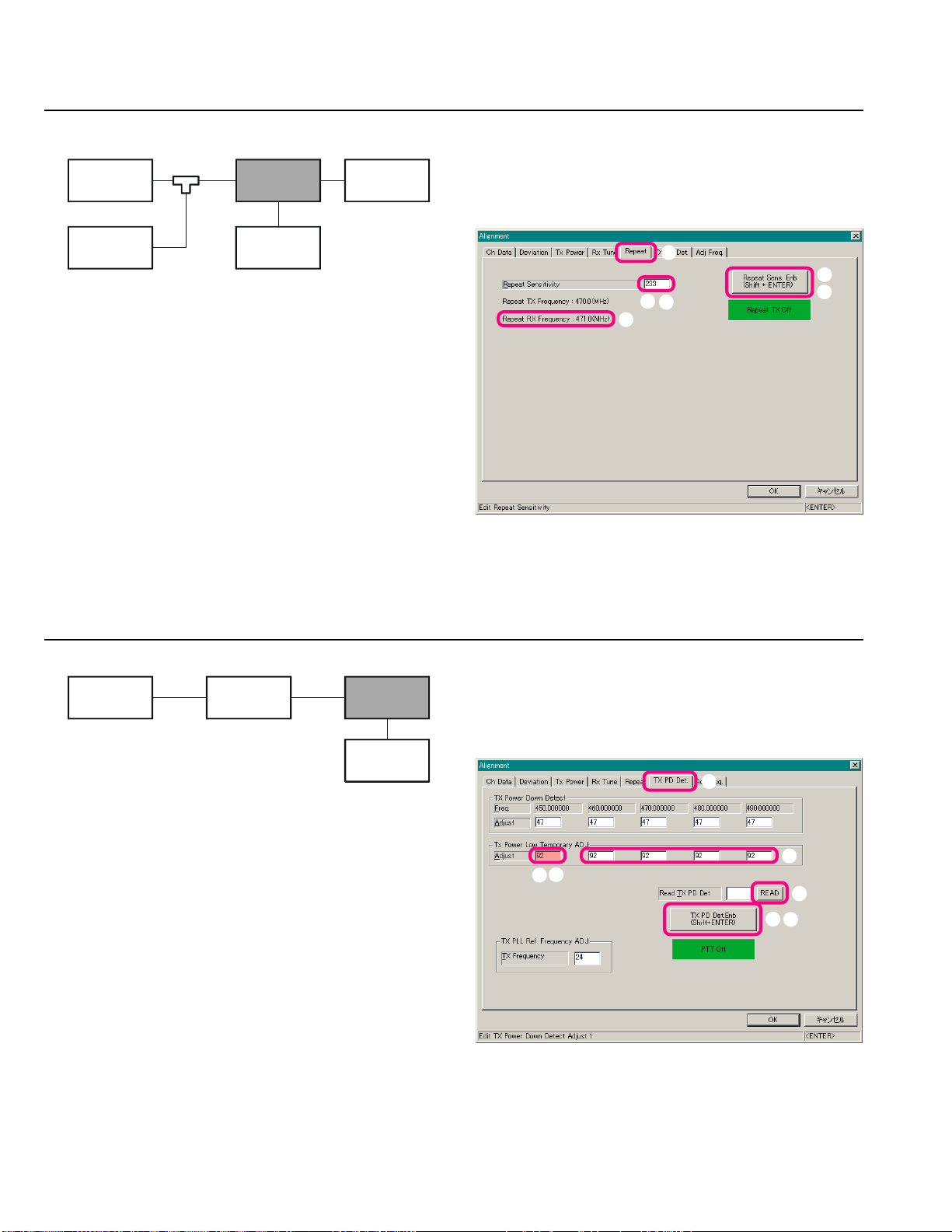
Repeat Sensitivity
Setup the test equipment as shown below.
Sampling
50-ohm
Dummy Load
Deviation
Meter
Open the “Alignment” window, then click the left
mouse button on the “Repeat” tab to move to the “Repeat” screen.
Set the RF Signal Generator output to the “Repeat RX
Frequency,” at a level of +40 dBµV, ±3.0 kHz deviation
with a 1 kHz audio tone.
Click the left mouse button on the “Repeat Sensitiv-
ity” box.
Click the left mouse button on the “Repeat Sens. Enb”
button to actitvate the transmitter (the “Repeat Sens.
Enb” label is changed to “Repeat TX Off”).
Coupler
TX ANT
VXR-9000
RX ANT
RF Signal
Generator
MIC
Computer
(
CE60
Press the [Page Up]/[Page Down] key so that the De-
viation Meter reading is 3.0 kHz ±0.2 kHz.
Click the left mouse button on the “Repeat TX Off”
)
button to disable the transmitter (the “Repeat TX Off”
label is returned to “Repeat Sens. Enb”).
TX Power Down Detect
Setup the test equipment as shown below.
50-ohm
Dummy Load
Open the “Alignment” window, then click the left
mouse button on the “TX PD Det.” tab to move to the
“TX PD Det.” screen.
Click the left mouse button on the “Adjust” box on the
“Low Band Edge Frequency” area of the “Tx Power
Low Temporary ADJ” field (highlighted in “pink”).
Click the left mouse button on the “TX PD Det. Enb”
button to actitvate the transmitter (the “TX PD Det.
Enb” label is changed to “PTT Off”).
Press the [Page Up]/[Page Down] key so that the
Power Meter reading is 5 W.
Click the left mouse button on the “READ” button to
save the “TX Power Down Detect” data.
Inline
Wattmeter
TX ANT
VXR-9000
Computer
(
CE60
MIC
Click the left mouse button on the “PTT Off” button
to disable the transmitter (the “PTT Off” label is returned to “TX PD Det. Enb”).
Repeat the above steps at the four points (box: frequen-
cies).
)
G-7
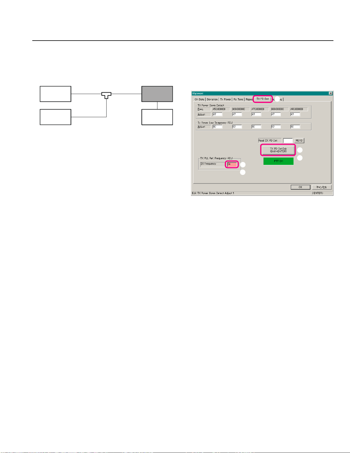
PLL Reference Frequency
g
Alignment
Important Note: (1) Do not this adjustment unless you have a
high-performance frequency counter. (2) This adjustment
needs to add a “Chip Resistor” on to the Main Unit. For further details contact to Vertex Standard.
Setup the test equipment as shown below.
Samplin
50-ohm
Dummy Load
Frequency
Counter
Open the “Alignment” window, then click the left
mouse button on the “TX PD Det.” tab to move to the
“TX PD Det.” screen.
Click the left mouse button on the “TX Frequency”
box (highlighted in “pink”).
Click the left mouse button on the “TX PD Det. Enb”
button to actitvate the transmitter (the “TX PD Det.
Enb” label is changed to “PTT Off”).
Coupler
TX ANT
VXR-9000
MIC
Computer
(
)
CE60
Press the [Page Up]/[Page Down] key so that the Fre-
quency Counter reading is “Low Band Edge Frequency” ±100 Hz.
Click the left mouse button on the “PTT Off” button
to disable the transmitter (the “PTT Off” label is returned to “TX PD Det. Enb”).
G-8

Alignment
Note:
G-9
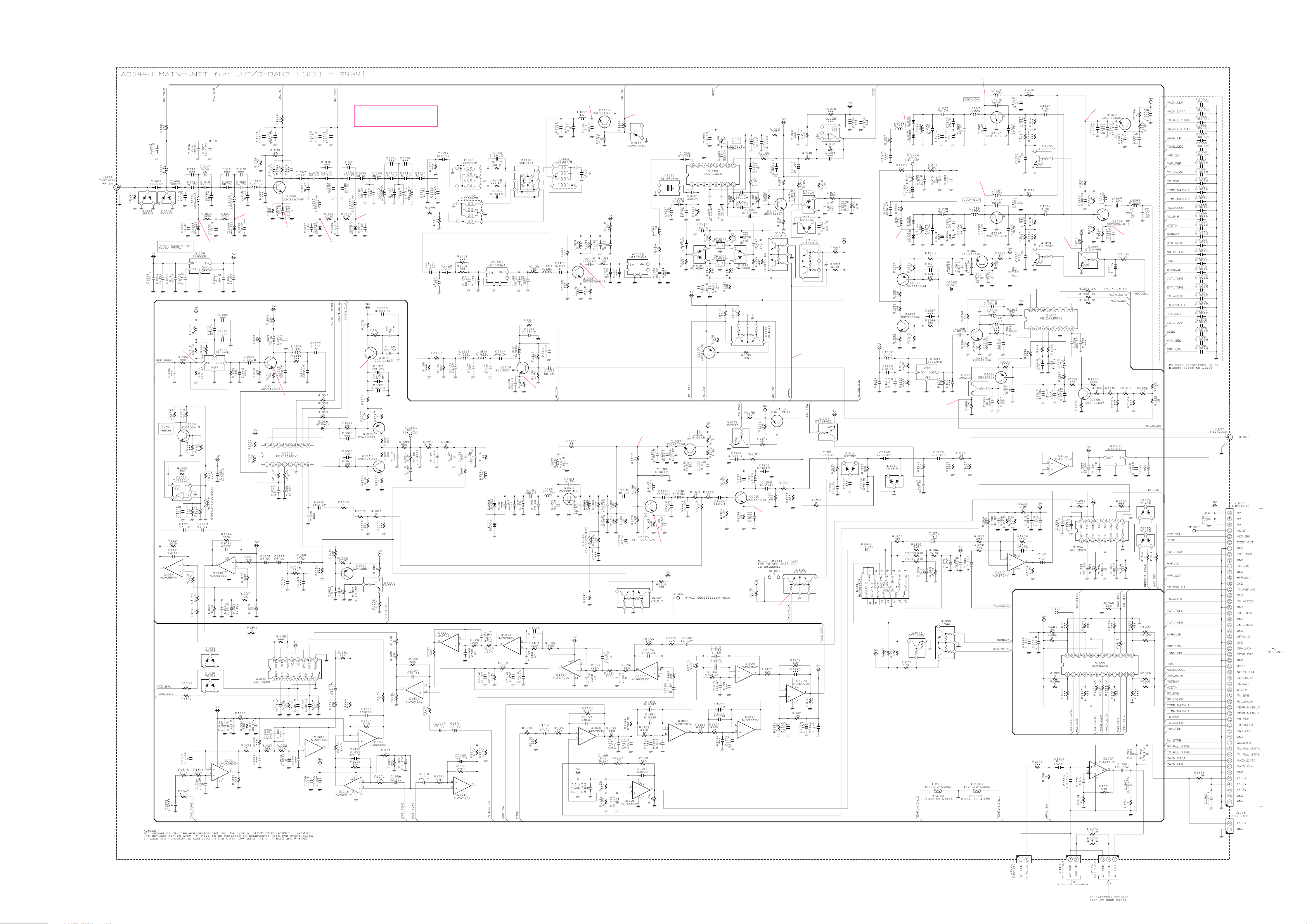
(
8.0 V
MAIN Unit (Lot. 1~2)
Circuit Diagram
)
2.2 V
2.2 V
1.3 V
2.2 V
Frequency: 470.20 MHz
2.2 V
(
468.80 MHz
4.9 V
)
7.1 V
8.9 V
0.9 V
(
8.4 V
)
8.0 V
0 V
(
4.2 V
8.9 V
)
2.3 V
1.5 V
0.4 V
WIDE: 0.1 V
NARROW: 7.5 V
8.6 V
1.3 V
LOCK: 0 V
UNLOCK: 5.0 V
8.0 V
0.5 V
2.3 V
LOCK: 0 V
UNLOCK: 5.0 V
H-1

MAIN Unit (Lot. 1~2)
Note
H-2
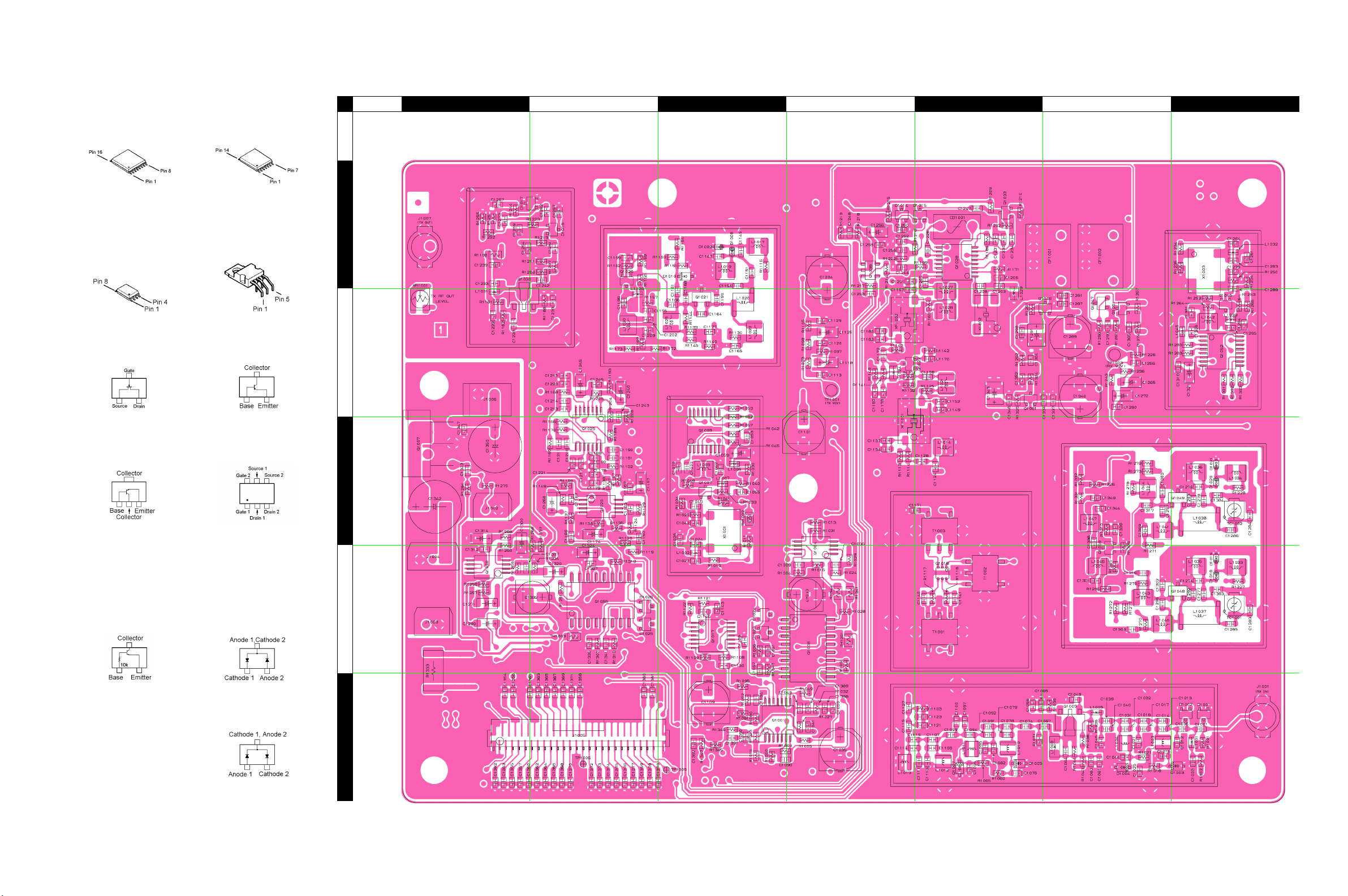
MAIN Unit (Lot. 1~2)
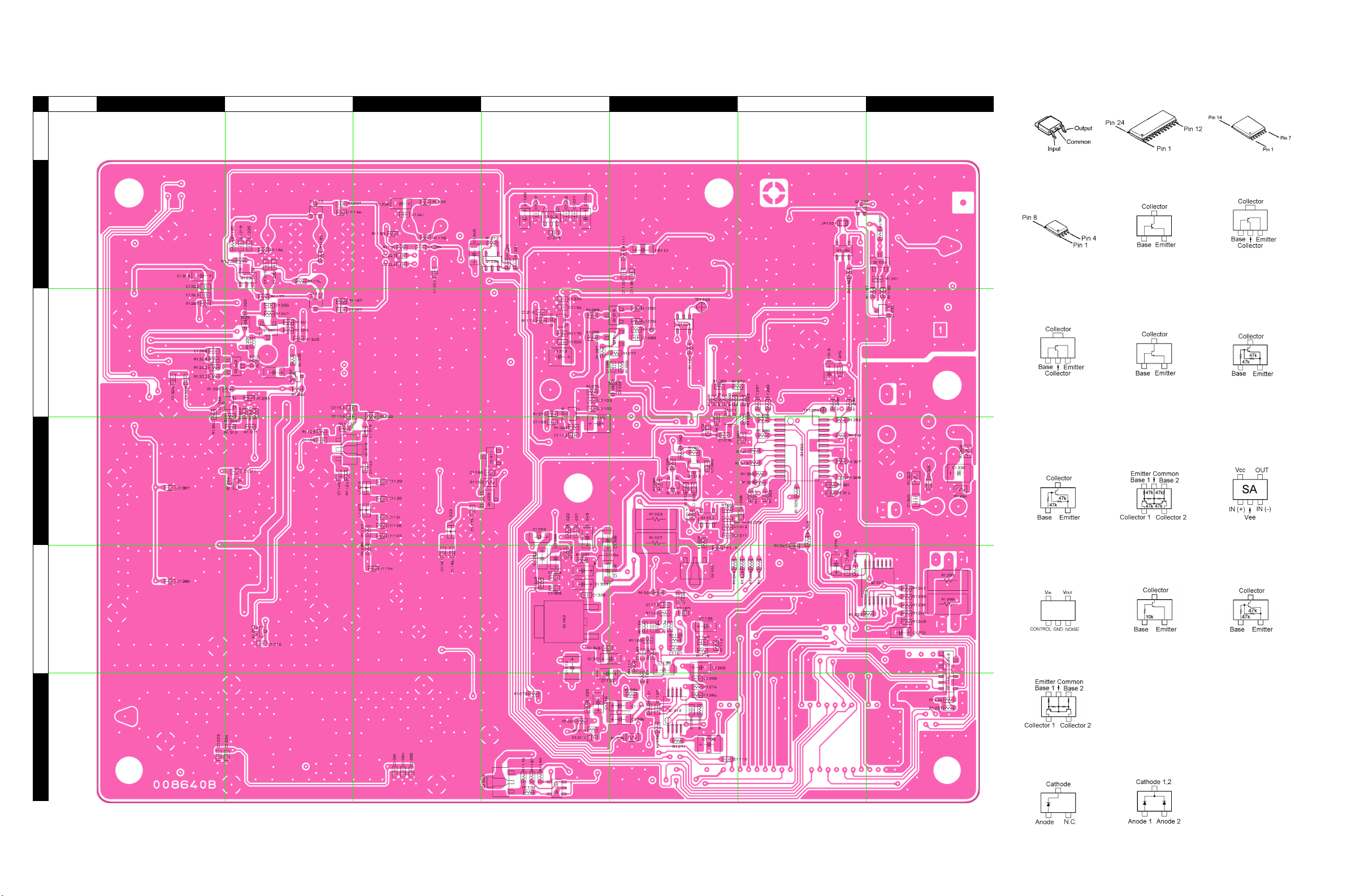
Parts Layout (Side A)
BA DC FE G
M51132FP
(Q1006, 1056)
MB15A02PFV1
(Q1008, 1052)
TA31136FN
(Q1028)
NJM2904V
(Q1004, 1020, 1050)
2SK508 (K52)
(Q1021, 1048,
1049)
NJM2902V
(Q1001, 1017, 1025)
TDA2003
(Q1057)
2SA1586Y (SY)
(Q1051)
1
2
3
2SC3357 (RK)
(Q1009, 1030)
2SC4116GR (LG)
(Q1007, 1033, 1045,
1046, 1061)
2SC5226 (R22)
(Q1022, 1026, 1059)
UN5215 (8E)
(Q1047)
SPM5001
(Q1018)
4
1SS302 (C3)
(D1001)
5
MA143 (MC)
(D1014, 1015, 1023,
1024, 1025, 1026)
RN739F (5F)
(D1002, 1016, 1017)
H-3
MAIN Unit (Lot. 1~2)
Parts Layout (Side B)
ba dc fe
g
L78M05T
(Q1062)
M62364FP
(Q1055)
BU4066BCFV
(Q1040)
1
NJM2904V
(Q1010)
2SA1162GR (SG)
(Q1014, 1041)
2SA1179 (M6)
(Q1034)
2SA1586Y (SY)
(Q1012)
2SB1122S (BE)
(Q1029)
2
2SC3357 (RK)
(Q1019)
2SD1664 (DA)
(Q1002)
2SC2712GR (LG)
(Q1015, 1042)
2SC2812 (LG)
(Q1023)
2SC4116GR (LG)
(Q1016, 1027, 1058)
DTA144EE (16)
(Q1037)
3
DTC144EE (26)
(Q1053, 1054, 1060)
DTC144EK (26)
(Q1043)
FMG2 (G2)
(Q1044)
TA75S01F (SA)
(Q1003)
4
TAR5S30
(Q1005)
5
XN1213 (9L)
(Q1024, 1031, 1035,
1036, 1039)
UN5215 (8E)
(Q1013)
UN5213 (8C)
(Q1032)
H-4
HZM5.6NB2 (562)
(D1011)
MA142WK (MU)
(D1012, 1013)
MAIN Unit (Lot. 3~24)
Circuit Diagram
H-5

MAIN Unit (Lot. 3~24)
Note
H-6
 Loading...