

Vertex Standard VX-820 Series, VX-820E Series Service Manual
VERTEX STANDARD CO., LTD.
4-8-8 Nakameguro, Meguro-Ku, Tokyo 153-8644, Japan
VERTEX STANDARD
US Headquarters
10900 Walker Street, Cypress, CA 90630, U.S.A.
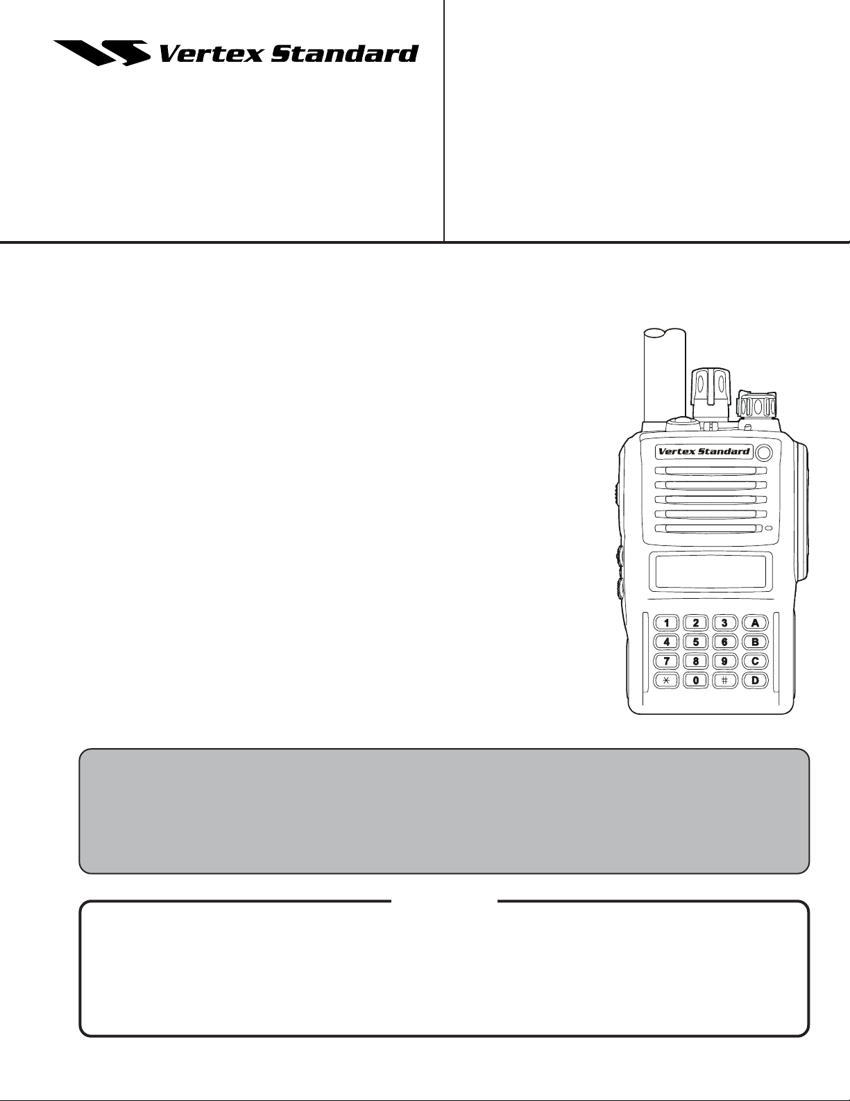
VX-820/-820E Series
UHF Band
Service Manual
©2009 VERTEX STANDARD CO., LTD. EC058U90D
YAESU UK LTD.
Unit 12, Sun Valley Business Park, Winnall Close
Winchester, Hampshire, SO23 0LB, U.K.
VERTEX STANDARD HK LTD.
Unit 5, 20/F., Seaview Centre, 139-141 Hoi Bun Road,
Kwun Tong, Kowloon, Hong Kong
VERTEX STANDARD (AUSTRALIA) PTY., LTD.
Normanby Business Park, Unit 14/45 Normanby Road
Notting Hill 3168, Victoria, Australia
Introduction
This manual provides the technical information necessary for servicing the VX-820 Series Transceiver.
Servicing this equipment requires expertise in handing surface-mount chip components. Attempts by non-qualified persons to service this equipment may result in permanent damage not covered by the warranty, and may be illegal in
some countries.
Two PCB layout diagrams are provided for each double-sided board in this
transceiver. Each side of the board is referred to by the type of the majority of
components installed on that side (“Side A” or “Side B”). In most cases one side
has only chip components (surface-mount devices), and the other has either a
mixture of both chip and leaded components (trimmers, coils, electrolytic capacitors, ICs, etc.), or leaded components only.
As described in the pages to follow, the advanced microprocessor design of the
VX-820 Series Transceiver allows a complete alignment of this transceiver to be
performed without opening the case of the radio; all adjustments can be performed from the front panel, using the “Alignment Mode” menu.
While we believe the information in this manual to be correct, VERTEX STANDARD assumes no liability for damage that may occur as a result of typographical or other errors that may be present. Your cooperation in pointing out any
inconsistencies in the technical information would be appreciated.
Important Note
After Lot. 11 of this transceiver was assembled using Pb (lead) free solder, based on the RoHS specification.
Only lead-free solder (Alloy Composition: Sn-3.0Ag-0.5Cu) should be used for repairs performed on this apparatus. The
solder stated above utilizes the alloy composition required for compliance with the lead-free specification, and any solder with
the above alloy composition may be used.
Contents
Specifications...........................................................2
Exploded View & Miscellaneous Parts .................4
Block Diagram ........................................................ 5
Circuit Description ................................................7
Alignment ................................................................9
Board Units (Schematics, Layouts & Parts)
MAIN Unit ....................................................... 15
Display Unit ..................................................... 47
Cable Unit ........................................................ 64
1

Specifications (VTX/EXP Version)
General
Frequency range: 400-470 MHz (Version A)
450-512 MHz (Version D, VTX)
450-520 MHz (Version D, EXP)
Channel / Group: 32 CH / 1 Group (w/o LCD version)
512 CH / 16 Groups (w/ LCD version)
Channel Spacing: 12.5/20/25 kHz
PLL Stepping: 5/6.25 kHz
Power Supply Voltage: 7.4 V
Current Consumption: 30 mA (Standby w/saver)
(Approx. @7.4 V) 75 mA (Standby)
200 mA (Receive)
1.9 A (Transmit)
Battery Life (Approx.): 7 hours (w/ FNB-V86LI)
11.5 hours (w/ FNB-V87LI)
Operating Temperature Range: –22 °F to +140 °F (–30 °C to +60 °C)
Frequency Stability: ±2.5ppm
Case Size (W x H x D): 2.3” x 3.8” x 1.5” (57.5 x 96.5 x 37.5 mm)
Weight (Approx.): 10.9 oz (310g) (w/FNB-V86LI, ATU-6, CLIP-920)
Receiver (Measurement per TIA/EIA-603)
Circuit Type: Double Conversion Super-heterodyne
Sensitivity (12dB SINAD): 0.25 μV/0.32 μV(W/N)
Adjacent Channel Selectivity: 75/70 dB (W/N)
Intermodulation: 75/70 dB (W/N)
Spurious Image Rejection: 75 dB
Audio output: 700 mW @ 16 ohms 5% THD
Transmitter (Measurement per TIA/EIA-603)
RF Power Output: 5/2.5/1/0.25 W
Modulation Type: Direct FM (16K0F3E/11K0F3E)
Maximum Frequency Deviation: ±2.5/±4.0/±5.0 kHz
Audio Distortion: Less than 3% @ 1kHz
Spurious Emissions: 70 dB below carrier
Specifications subject to change without notice or obligation.
2

Specifications (EU Version)
General
Frequency range: 400-470 MHz
Channel / Group: 32 CH / 1 Group (w/o LCD version)
512 CH / 16 Groups (w/ LCD version)
Channel Spacing: 12.5/20/25 kHz
PLL Stepping: 5/6.25 kHz
Power Supply Voltage: 7.4 V
Current Consumption: 30 mA (Standby w/saver)
(Approx. @7.4 V) 75 mA (Standby)
200 mA (Receive)
1.9 A (Transmit)
Battery Life (Approx.): 7 hours (w/ FNB-V86LI)
11.5 hours (w/ FNB-V87LI)
Operating Temperature Range: –30 °C to +60 °C
Frequency Stability: ±2.5ppm
Case Size (W x H x D): 57.5 x 96.5 x 37.5 mm
Weight (Approx.): 310g (w/FNB-V86LI, ATU-6, CLIP-920)
Receiver
Circuit Type: Double Conversion Super-heterodyne
Sensitivity (12dB SINAD): 0.25 μV/0.32 μV(W/N)
Adjacent Channel Selectivity: 75/65 dB (W/N)
Intermodulation: 65 dB (W/N)
Spurious and Image Rejection: 70 dB
Num & Noise: 48/42 dB (W/N)
Audio output: 700 mW @ 16 ohms 5% THD
Transmitter
RF Power Output: 5/2.5/1/0.25 W
Modulation Type: Direct FM (16K0F3E/11K0F3E)
Maximum Frequency Deviation: ±2.5/±4.0/±5.0 kHz
FM Hum & Noise: 45/40 dB (W/N)
Audio Distortion: Less than 3% @ 1kHz
Spurious Emissions: –36 dBm @under 1 GHz
–30 dBm @above 1 GHz
Measurements per: EN 300 086 standards unless noted above.
Specifications subject to change without notice or obligation.
3
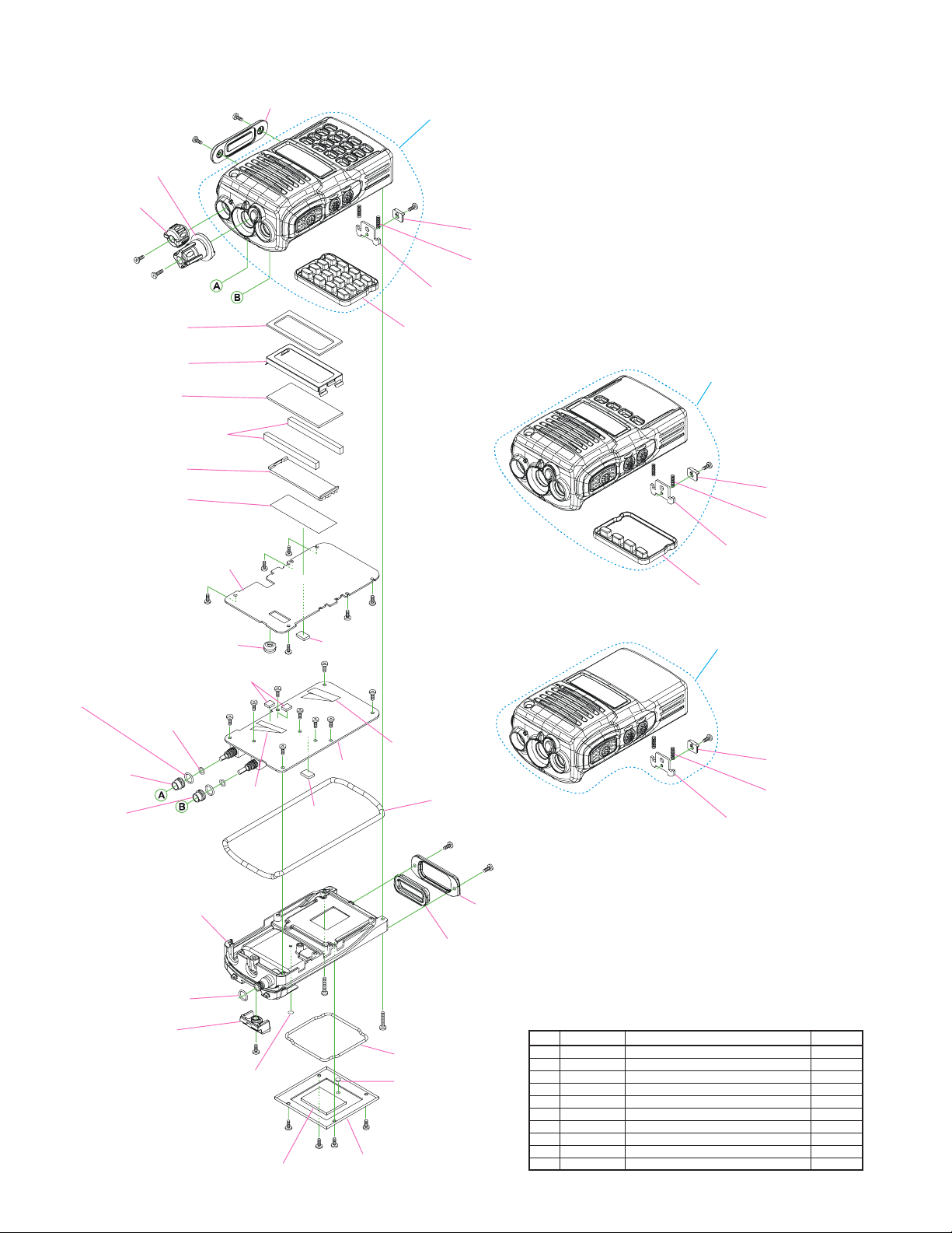
Exploded View & Miscellaneous Parts
RA0611500
ROTARY KNOB (CH)
RA0601700
ROTARY KNOB (VOL)
RA0727300
PAD
RA068970A
FRAME
G6090163
LCD
RA0663700 (x2 pcs)
INTER CONNECTOR
RA0689100
LIGHT GUIDE
RA0698000
REFERECTOR
SHEET
RA0712300
HOLDER RUBBER (SW)
RA0603700 (x2 pcs, WP: STD)
RA0811600 (x2 pcs, WP: HIGH)
O RING
RA060450A
SPECIAL NUT (M)
RA060460A
SPECIAL NUT (L)
RA0603600 (x2 pcs)
O RING (1x4.2)
CP8256001 (IS: OFF)
CP8256002 (IS: ON, WP: STD)
CP8256001 (IS: ON, WP: HIGH)
REAR CASE ASSY
DISPLAY UNIT
RA0731500 (x2 pcs)
PAD (E1)
T9207216
FW-ASSY
RA0601800
SIDE COVER
RA0697900
SHEET (FET)
RA0727300
PAD (LCD)
MAIN UNIT
CP8254003 (Water Proof: Standard)
CP8254006 (Water Proof: High Spec.)
PANEL ASSY (16 KEY)
RA0688700
LATCH NAIL
RA0745400 (x2 pcs)
COIL SPRING
RA060400B
LATCH PLATE
RA0663800
RUBBER KNOB (16KEY)
CP8254002 (Water Proof: Standard)
CP8254005 (Water Proof: High Spec.)
PANEL ASSY (4 KEY)
RA0688700
LATCH NAIL
RA0745400 (x2 pcs)
COIL SPRING
RA060400B
LATCH PLATE
RA070350A
RUBBER KNOB (4KEY)
CP8254001 (Water Proof: Standard)
CP8254004 (Water Proof: High Spec.)
PANEL ASSY (NO KEY)
T9207217
FW-ASSY
RA0602800
GASKET
RA060400B
LATCH PLATE
RA0688700
LATCH NAIL
RA0745400 (x2 pcs)
COIL SPRING
RA0681900
HOLDER PLATE (POW)
RA0607300 (WP: STD)
RA0811500 (WP: HIGH)
O RING (1.8x5.3)
RA0602000
COVER (BAT)
WP: STD = Water Proof: Standard
WP: HIGH = Water Proof: High Spec.
4
RA0729100
BLIND SHEET
RA0697400
PAD (ACS)
RA0664000
RUBBER PACKING (POW)
Non-designated parts are available only as
part of a designated assembly.
RA0663500
GASKET (ACS)
RA0731400 (WP: STD)
RA0775800 (WP: HIGH)
SHEET
RA068950A
COVER (ACS)
Ref.
VXSTD P/N
RA0606200
U00103002
U07230227
U07A35220
U07A60220
U44104002
U44110020
U51106027
U9900094
RA0604400
SPECIAL SCREW
PAN HEAD SCREW
PAN HEAD SCREW
PAN HEAD SCREW
PAN HEAD SCREW
TAPTITE SCREW
TAPTITE SCREW
HEX SOCKET BOLT
TAPTITE SCREW
SPECIAL SCREW
Description
(M2.6X5)
M2X3NI
M2X3BSUS #2
M2X3.5 SUS #2
M2X6 SUS #2
M2X4NI
2X10SUS
M2X6BSUS
M2X5NI #2
(M3X6)
Qty.
2
1
1
4
4
12
2
2
2
1
Ú1: w/ LCD, Ú2: w/o LCD
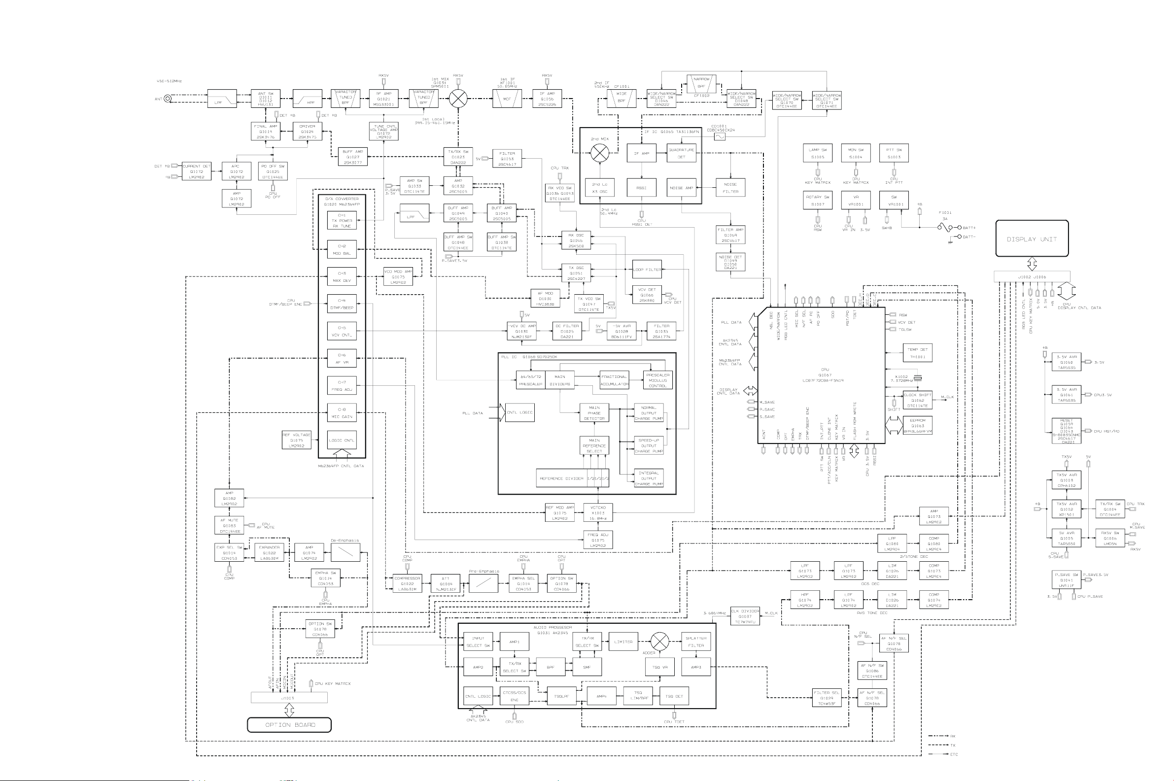
Block Diagram
Main Unit
5
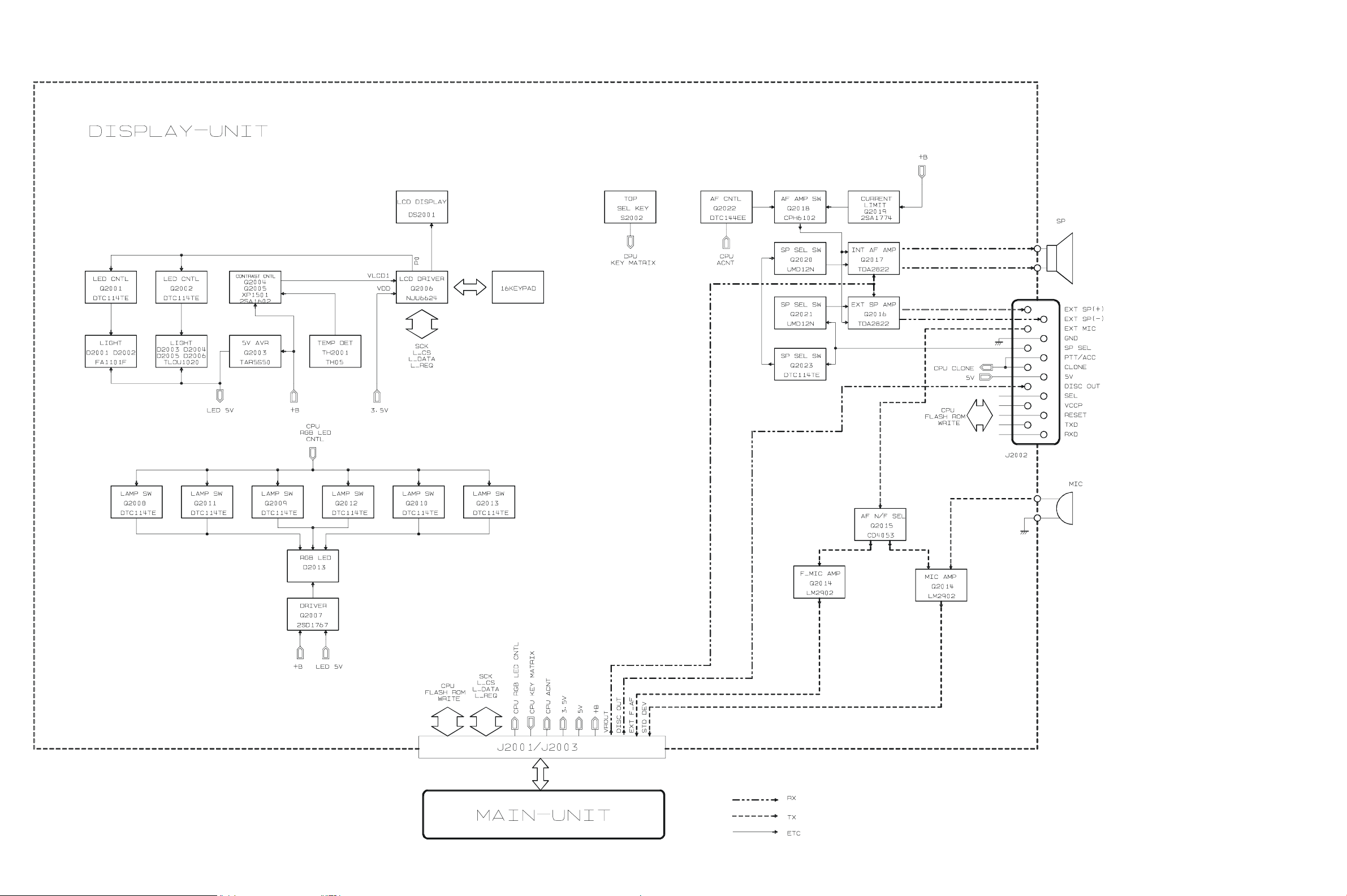
Block Diagram
Display Unit
6

Circuit Description
1. Circuit Configuration by Frequency
The receiver is a double-conversion superheterodyne
type, with a first Intermediate Frequency (IF) of 50.85
MHz and a second IF of 450 kHz. Incoming signals
from the antenna are mixed with the local signal from
the VCO/PLL to produce the first IF of 50.85 MHz.
The signals are then mixed with the 50.4 MHz second local oscillator output to produce the 450 kHz
second IF. This is detected to give the demodulated
signal. The transmit signal frequency is generated
by the PLL VCO, and modulated by the signal from
the microphone. It is then amplified and sent to the
antenna.
2. Receiver System
2-1. Front-end RF amplifier
Incoming RF signals from the antenna are delivered
to the Main Unit and pass through a Low-pass filter,
antenna switching diode D1011 (HVU131), and a
high pass filter, and undesired out-of-band signals
are then removed by a varactor-diode-tuned bandpass filter D1013 and D1015 (both 1SV323). The re-
sidual signals are amplified by Q1021 (MSG33001)
and then pass through a varactor-diode-tuned image-stripping band pass filter D1020 and D1022 (both
1SV323) prior to delivery to the 1st mixer.
2-2. First Mixer
The 1st mixer consists of Q1034 (SPM5001), T1001,
T1002, and T1003. Buffered output from the VCO is
amplified by Q1032 (2SC5005) to provide a pure first
local signal between 349.15 and 419.15 MHz (Version A) or 399.15 and 461.15 MHz (Version D) for
injection to the first mixer. The IF signal then passes
through monolithic crystal filter XF1001 (±5.5 kHz
BW) to strip away undesired mixing products.
filter CF1001 (wide channels), CF1002 (narrow channels) to strip away all but the desired signal, and is
applied to the limiter amplifier in Q1065
(TA31136FN), which removes amplitude variations
in the 450 kHz IF, before detection of the speech by
the ceramic discriminator CD1001.
2-4. Audio amplifier
Detected audio from Q1065 (TA31136FN) is applied
to Q1031 (AK2345) and is fed to the bandpass filter
inside Q1031 (AK2345).
If an optional signaling unit is installed, Q1078
(CD4066BPWR) is set to “OFF,” and the AF signal
from Q1032 (AK2345) is fed to the optional unit. If a
signaling unit is not installed, Q1078
(CD4066BPWR) is switched “ON,” and the signal
passes through Q1078 (CD4066BPWR). The signal
then proceeds through the de-emphasis stage and
the expander at Q1022 (LA8630M). When the ex-
pander function is off, the signal will be bypassed
via Q1014 (CD4053BPWR). The output signal of the
expander (or a signal from de-emphasis) goes
through AF mute switch Q1083 (DTC114TE) and is
amplified by Q1082 (LM2902PWR). The output from
Q1082 LM2902PWR) is amplified by the AF power
amplifier Q2017 (TDA2822) after passing through
the AF volume control Q1020 (M62364FP).
put of Q2017 (TDA2822) drives the internal speaker.
2-5. Squelch Circuit
There are 13 levels of squelch setting, from “0” to
“12.” The level “0” corresponds to an “open” squelch.
The level “1” is the lowest squelch threshold setting
level, and level “11” means tight squelch. From “2”
to “10” are intermediate, increasingly-tight settings.
The level “12” represents carrier squelch.
The out-
2-3. IF Amplifier
The first IF signal is amplified by Q1056 (2SC5226).
The amplified first IF signal is applied to FM IF subsystem IC Q1065 (TA31136FN) which contains the
second mixer, second local oscillator, limiter amplifier, noise amplifier, and S-meter amplifier. The signal from reference oscillator X1003 is multiplied by
three by Q1065 (TA31136FN), and then is mixed with
the IF signal to produce a 450 kHz second IF.
The second IF signal then passes through the ceramic
2-5-1. Noise Squelch
The Noise Squelch circuit is composed of the
bandpass filter at Q1065 (TA31136FN), noise ampli-
fier Q1069 (2SC4617), and noise detector D1049/
D1050 (both DA221). When a carrier is not being re-
ceived, the noise components passed from demodulator Q1065 (TA31136FN) are amplified by Q1069
(2SC4617), fed through bandpass filter Q1065
(TA31136FN), detected as a DC voltage by D1049/
D1050 (both DA221), and applied to pin 16 (the A/D
7

Circuit Description
port) of Q1067 (CPU: LC87F5BP6A). When a carrier is received, the DC voltage becomes low because
the noise is compressed. When the detected voltage
to the CPU is high, the CPU stops AF output by setting Q1083 (DTC114TE) “OFF” (by making pin 59
of the CPU “High” level). When the detection voltage is low, the CPU switches Q1083 (DTC114TE)
“ON” by making pin 59 “Low,” and the AF signal is
allowed to flow.
2-5-2. Carrier Squelch
The pin 15 (A/D port) of CPU Q1067 (LC87F5BP6A)
detects the RSSI voltage output from Q1065
(TA31136FN) at pin 12, and controls the AF output.
The RSSI output voltage changes according to the
signal strength of carrier; a stronger signal makes
the RSSI voltage higher. The processing of the AF
signal control is same as Noise Squelch, except that
the switching threshold is adjusted so as to be 3 dB
higher than the “tight squelch” sensitivity.
The high frequency signal components are amplified by Q1075 (LM2902PWR), and their level is set
by Q1020 (M62364FP) to establish proper balance
of the level between high- and low-frequency components. After that, the signals modulate the transmit carrier via modulator D1030 (1SV286) of the
VCO.
3-2. Drive and Final Amplifier Stages
The modulated signal from VCO Q1051 (2SC4227)
is buffered by Q1040 (2SC5005) and amplified by
Q1032 (2SC5005). Then the signal is buffered by
Q1027 (2SK3077) for delivery to the final amplifier
driver Q1024 (2SK3475). The low-level transmit signal is then applied to Q1019 (2SK3476) for final am-
plification up to 5 watts output power. The transmit
signal then passes through the antenna switch D1012
(HVU131) and is low-pass filtered to suppress harmonic spurious radiation before delivery to the antenna.
3. Transmitter System
3-1. MIC Amplifier
The AF signal from the internal microphone (pin 21
of J2002 on the Display Unit) or an external microphone (pin 6 of J2002 on the Display Unit) passes
through microphone selection switch Q2015
(CD4053BPWR) and is amplified by microphone
amplifier Q2014 (LM2904PWR), thereafter passing
through the microphone gain controller, Q1020
(M62364FP). The AF signal then passes through
compandor Q1022 (LA8630M). When not using the
compandor, the CPU bypasses the compandor circuit and feeds the signal to the pre-emphasis circuit.
Q1078 (CD4066BPWR) becomes “OFF” when an op-
tional signaling unit is attached, and the AF signal
from Q1022 (LA8630M) is redirected via the signaling unit. If a signaling unit is not installed, Q1078
(CD4066BPWR) becomes “ON,” the signal bypasses
Q1078 (CD4066BPWR), and it instead is applied to
the pre-emphasis amplifier Q1031 (AK2345). The sig-
nal passes through the limiter and splatter filter of
Q1031 (AK2345), and is adjusted for proper devia-
tion at Q1020 (M62364FP). The low frequency sig-
nal components (CTCSS, DCS, etc.) are then amplified by Q1075 (LM2902PWR) and used for direct
modulation of the reference oscillator, TCXO X1003.
3-3. Automatic Transmit Power Control
The current detector Q1072 (NJM12902V) detects the
current drawn by Q1019 (2SK3476) and Q1024
(2SK3475), and converts the current difference to a
voltage difference. The output from the current detector Q1072 (NJM12902V) is compared with the reference voltage and amplified by the power control
amplifier Q1072 (NJM12902V). The output from
Q1072 (NJM12902V) controls the gate bias of the fi-
nal amplifier Q1019 (2SK3476) and the driver Q1024
(2SK3475). The reference voltage switches among
four values of TX Power (“High,” “Low3,” “Low2,”
and “Low1”), as controlled by Q1020 (M62364FP).
3-4. PLL Frequency Synthesizer
The frequency synthesizer consists of PLL IC Q1068
(SA7025DK), the VCO, TCXO (
amplifier. The output frequency from the TCXO is
16.8 MHz, and the tolerance is ±2.5 ppm (in the temperature range —30 °C to +60 °C).
3-4-1. VCO (Voltage-Controlled Oscillator)
While the radio is receiving, the RX oscillator Q1046
(2SK508) in the VCO generates a programmed frequency between 349.15 and 419.15 MHz (Version A)
or 399.15 and 461.15 MHz (Version D) as the 1st lo-
X1003), and buffer
8

Circuit Description
cal signal. While the radio is transmitting, the TX oscillator Q1051 (2SC4227) in the VCO generates a frequency between 400 and 470 MHz (Version A) or 450
and 512 MHz (Version D) (the actual transmitting
frequency). The output from the oscillator is amplified by buffer amplifier Q1040 (2SC5005) and becomes the output of the VCO. The output from VCO
is divided: one part is amplified by Q1049 (2SC5005)
and fed back to the PLL IC at pin 5. The other is amplified by Q1032 (2SC5005) and, in case of the re-
ception, it is fed via D1023 (DAN222) to the mixer as
the 1st local signal. On transmit, it is fed via D1023
(DAN222) to buffer amplifire Q1027 (2SK3077), and
passed through the final amplifier driver Q1024
(2SK2375) to the final amplifier Q1019 (2SK2376).
3-4-2. VCV (Varactor Control Voltage) Control
The tuning voltage (VCV) of the VCO establishes the
lock range of the VCO by controlling the anode of a
varactor diode using a negative voltage and the control voltage from PLL IC Q1068 (SA7025DK). The
negative voltage is fed to the varactor diode after
conversion to a negative value at Q1030 (NJM2130F),
using the output voltage of the D/A converter, Q1020
(M62364FP).
3-4-3. PLL
The PLL IC Q1068 (SA7025DK) consists of a refer-
ence divider, main divider, phase detector, charge
pumps and a fractional accumulator. The reference
frequency from TCXO is applied to pin 8 of the PLL
IC Q1068 (SA7025DK) and is divided by the reference divider. This IC is a decimal point dividing PLL
IC, and the dividing ratio becomes 1/8 of the usual
PLL frequency step. Therefore, the output of reference divider is 8 times the frequency of the channel
step. For example, when the channel steps are set to
5 kHz, the output of reference divider becomes 40
kHz. The feedback signal from the VCO applied to 5
pin of the PLL IC Q1068 (SA7025DK) is divided ac-
cording to the dividing ratio so as to become the same
frequency as that of the output of reference divider.
These two signals are compared by the phase detector, and a phase difference pulse is generated. The
phase difference pulse and the pulse from the fractional accumulator pass through the charge pumps
and low-pass filter, producing a DC voltage (VCV)
to control the VCO. The oscillation frequency of the
VCO is therefore locked via the control of this DC
voltage. The PLL serial data from the CPU Q1067
(LC87F5BP6A) is sent with three lines of data: SDO
(pin 20), SCK (pin 22) and PSTB (pin 27). The lock
condition of the PLL is sent from the UL (pin 17) terminal, and UL becomes “High” at the time of a
proper lock condition and becomes “Low” at the time
of an unlocked condition. The CPU always watches
over the UL condition, and when it becomes “Low”
(unlocked condition), the CPU Q1067
(LC87F5BP6A) prohibits transmission and reception.
9

Circuit Description
Note
10

Alignment
Introduction
The VX-820 series is carefully aligned at the factory
for the specified performance across the frequency
range specified for each version. Realignment should
therefore not be necessary except in the event of a
component failure, or altering version type. All component replacement and service should be performed only by an authorized Vertex Standard rep-
resentative, or the warranty policy may be void.
The following procedures cover the sometimes critical and tedious adjustments that are not normally
required once the transceiver has left the factory.
However, if damage occurs and some parts subsequently are placed, realignment may be required. If
a sudden problem occurs during normal operation,
it is likely due to component failure; realignment
should not be done until after the faulty component
has been replaced.
We recommend that servicing be performed only by
authorized Vertex Standard service technicians who
are experienced with the circuitry and fully equipped
for repair and alignment. Therefore, if a fault is suspected, contact the dealer from whom the transceiver was purchased for instructions regarding repair.
Authorized Vertex Standard service technicians realign all circuits and make complete performance
checks to ensure compliance with factory specifications after replacing any faulty components.
Those who do undertake any of the following alignments are cautioned to proceed at their own risk.
Problems caused by unauthorized attempts at realignment are not covered by the warranty policy.
Also, Vertex Standard reserves the right to change
circuits and alignment procedures in the interest of
improved performance, without notifying owners.
The following test equipment (and thorough familiarity with its correct use) is necessary for complete
realignment. Correction of problems caused by misalignment resulting from use of improper test equipment is not covered under the warranty policy. While
most steps do not require all of the equipment listed, the interactions of some adjustments may require
that more complex adjustments be performed afterwards. Do not attempt to perform only a single step
unless it is clearly isolated electrically from all other
steps. Have all test equipment ready before beginning, and follow all of the steps in a section in the
order presented.
Required Test Equipment
RF Signal Generator with calibrated output level
at 1 GHz
Deviation Meter (linear detector)
In-line Wattmeter with 5 % accuracy at 1 GHz
50 Ohm RF Dummy Load with power rating 10
W at 1 GHz
16 Ohm AF Dummy Load (Attention : Audio out-
put is BTL output)
Regulated DC Power Supply (standard 7.5 V DC,
3 A)
Frequency Counter with 0.2 ppm accuracy at 1
GHz
Audio Generator
AC Voltmeter
DC Voltmeter
UHF Sampling Coupler
IBM PC / compatible Computer with Microsoft®
Windows® 95 or later operating system
Vertex Standard CE59 (version 2.06 or later) Align-
ment program and CT-109 PC Programming
Ú
Cable or FIF-10A
gramming Cable
USB Interface/CT-108 PC Pro-
Under no circumstances should any alignment be
attempted unless the normal function and operation
of the transceiver are clearly understood, the cause
of the malfunction has been clearly pinpointed and
any faulty components replaced, and realignment
determined to be absolutely necessary.
: When using the FIF-10A USB Interface, requires
Ú
the Windows® 2000 or Windows® XP
11
Alignment
Alignment Preparation & Precautions
A 50-Ohm RF Dummy Load and in-line wattmeter
must be connected to the main antenna jack in all
procedures that call for transmission, except where
specified otherwise. Correct alignment is not possible with an antenna.
After completing one step, read the following step
to determine whether the same test equipment will
be required. If not, remove the test equipment (except dummy load and wattmeter, in connected) before proceeding.
Correct alignment requires that the ambient temperature be the same as that of the transceiver and test
equipment, and that this temperature be held constant between 68 and 86 °F (20 ~ 30 °C). When the
transceiver is brought into the shop from hot or cold
air, it should be allowed time to come to room temperature before alignment.
Whenever possible, alignments should be made with
oscillator shields and circuit boards firmly affixed in
place. Also, the test equipment must be thoroughly
warmed up before beginning.
Setup the test equipment as shown for transceiver
alignment, apply 7.5 V DC power to the transceiver.
Refer to the drawings above for Alignment Points.
The transceiver must be programmed for use in the
intended system before alignment is attempted. The
RF parameters are loaded from the file during the
alignment process.
In order to facilitate alignment over the complete
switching range of the equipment it is recommended that the channel data in the transceiver is preset
as the chart below.
CHANNEL
BAND-LOW
BAND-MID
BAND-HIGH
VERSION A
400.000 MHz
435.000 MHz
470.000 MHz
VERSION D
450.000 MHz
480.000 MHz
512.000 MHz
The alignment mode is accessed by “Alignment
mode” command from the computer, and the alignment tool operates it automatically. During the alignment mode, normal operation is suspended. Use the
alignment tool program running on PC.
Note: Signal levels in dB referred to in the alignment
procedure are based on 0 dBm EMF = 1 mV.
Deviation
Meter
Signal Generator
MIC/SP
COM Port or USB Jack
Frequency
Counter
CT-109 or FIF-10/CT-108
30 dB PAD
Inline
Wattmeter
MIC/SP
Power Supply
7.5 VDC
COM Port or USB Jack
ANT
VX-820
CT-109 or FIF-10/CT-108
TRANSMITTER SECTION ALINGMENT SETUP RECEIVER SECTION ALINGMENT SETUP
RF
ANT
VX-820
Power Supply
7.5 VDC
12
Alignment
The Alignment Tool Outline
Installation the tool
Install the CE59 (version 2.06 or later) to your PC.
The re-alignment for VX-820 series uses the
“Alignment“ menu of CE59.
Action of the switches
When the transceiver is in the “Alignment mode,“ the
actions of the PTT switch and keys are ignored. All of
the commands are remotely controlled by the PC.
Basic sequence
The data displayed in screen of this tool is temporary data, and you must take care to ensure the preservation of the command sequence which is specified below.
1. Enter the “Alignment mode“
2. Upload data from radio
3. Edit/set alignment data
4. Download data to radio
When you finish one alignment parameter, the tool
will ask you “Save the Aligned Data?“ If you select
“Yes,“ the temporary data will updated. If you select “No,“ the tool will not update the temporary data
and the setting will return to its original value.
Basic Alignment Mode
The Basic Alignment mode allows you to align the
entire radio. The value of each parameter can be
changed to the desired position by use of the “” /
“” and up/down arrow keys, along with direct
number input and dragging of the PC mouse.
To enter the Basic Alignment Mode, select “Basic
Alignment” in the main “Radio” menu. It will start
to “Upload” the written personalized data from the
radio. Pressing the “OK” button will then start the
Basic Alignment Mode.
Note: when all items are to be aligned, it is strongly
recommended to align them according to following
sequence. Detailed information for each step may be
found in the “Help” file within CE59 (Clone Editor).
1. RX VCO Tune Voltage (RX VCO)
2. TX VCO Tune Voltage (TX VCO)
3. PLL Reference Frequency (Frequency)
4. RX Sensitivity (RX Tune)
5. Squelch (SQL)
6. TX Power
7. Maximum Deviation <Wide>
8. Maximum Deviation <Narrow>
9. Sub Audio Deviation <CTCSS>
10. Sub Audio Deviation <DCS>
BATTERY TERMINAL POLARITY
13
Alignment
CH (C
HANNEL-BY-CHANNEL
) Fine Alignment Mode
The CH Fine Alignment Mode allows you to align
the radio separately for every operating channel. The
value of each parameter can be changed to the desired position using the “” / “” and up/down
arrow keys, direct number input, and by dragging
the PC mouse.
To enter the CH Fine Alignment Mode, select “CH
Fine Alignment” in the main “Radio” menu. It will
start to “Upload” the written personalized data from
the radio. Pressing the “OK” button will then start
the CH Fine Alignment Mode.
Note: Detailed information for each step may be found
in the “Help” file within CE59 (Clone Editor).
Pin 1: WHITE
Pin 2: RED
VXSTD P/N: T9207094
Pin 3: SHIELD
Pin 4: BLACK
Pin 5: BLUE
Pin 6: YELLOW
Pin 7: GRAY
Pin 8: GREEN
Pin 9: PURPLE
Pin 10: ORANGE
Pin 11: L_GREEN
Pin 12: CLEAR
Pin 13: PINK
Pin 14: BROWN
220 µF
16-Ohm 2W
220 µF
10 µF
27 k-Ohm
1/2 OUTPUT LEVEL
AF METER
AUDIO GENERATOR
PTT SW
2.2 k-Ohm
Pin 2: SP
Pin 4: MIC
Pin 6: PTT/AC C
Pin 10: SEL
Pin 12: RESET
Pin 14: RXD
14
(- )
Pin 8: 5V
Note!
Because of the bridge audio amplifier circuit
used in the
-
Pin 1: SP (+
Pin 3: GND
Pin 5: SELECT
Pin 7: CLONE
Pin 9: DISC OUT
Pin 11: VCCP
Pin 13: TXD
)
and use a simple audio load test adapter as
shown in the schematic diagram, when conducting receiver alignment steps.
Do not connect either side of the speaker leads
to chassis “ground.”
AF TEST ADAPTER SCHEMATIC
, it is necessary to construct
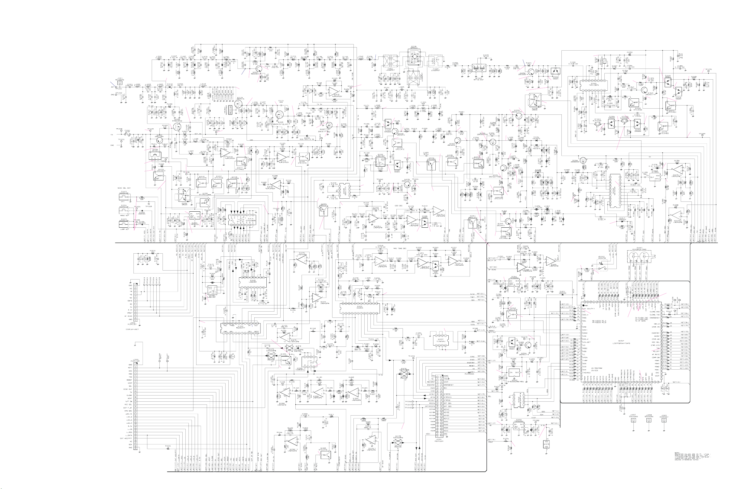
Main Unit (Lot. 1 ~ 2)
Circuit Diagram
–8.5 dBμV emf
@485.1 MHz
RX: 7.4 V
TX: 7.1 V
RX: 7.4 V
TX: 6.7 V
RX: 5.0 V
TX: 4.3 V
RX: 5.0 V
TX: 0.1 V
SW ON: 0 V
SW OFF: 3.5 V
RX: 0 V
TX: 0.8 V
PWR ON: 0 V
PWR OFF: 6.7 V
RX: 0 V
TX: 5.0 V
RX: 0.1 V
TX: 3.4 V
PWR ON: 7.4 V
PWR OFF: 1.1 V
TX: 7.1 V
SAVE ON: 0 V
SAVE OFF: 4.9 V
TX: 0 V
7.4 V
PWR ON: 1.7 V
PWR OFF: 0 V
SAVE ON: 0 V
SAVE OFF: 3.4 V
TX: 0 V
PWR ON: 5.0 V
PWR OFF: 0 V
RX: 0 V
TX: 5.0 V
3.5 V
RX: 7.4 V
TX: 6.9 V
–10.5 dBμV emf
@485.1 MHz
RX: 4.1 V
TX: 0 V
RX: 7.4 V
TX: 6.9 V
RX: 1.3 V
TX: 0 V
RX: 0 V
TX: 2.0 V
RX: 1.5 V
TX: 0 V
RX: 7.4 V
TX: 6.9 V
RX: 3.0 V
TX: 0 V
RX: 0.7 V
TX: 0 V
RX: 3.1 V
TX: 0 V
2.5 V @25 °C
RX: 0 V
TX: 3.1 V
RX: 0 V
TX: 3.9 V
RX: 0 V
TX: 3.0 V
3.5 V
MUTE: 3.5 V
BUSY: 0.5 V
TX: 0.5 V
RX: 0 V
TX: 1.2 V
MUTE: 0 V
BUSY: 3.5 V
TX: 3.5 V
RX: 1.6 V
TX: 0.6 V
@485.1 MHz
5.1 V
–0.2 dBμV emf
@485.1 MHz
RX: 0 V
TX: 3.9 V
RX: 3.2 V
TX: 0 V
RX: 2.5 V
TX: 3.2 V
RX: –2.1 V
TX: –1.3 V
@485.1 MHz
RX: –4.9 V
TX: –5.0 V
0.1 V
RX: 0.8 V
TX: 0.9 V
RX: –1.7 V
TX: –1.0 V
@485.1 MHz
RX: –4.8 V
TX: –5.0 V
MUTE: 0 V
BUSY: 0.3 V
TX: 0 V
3.5 V
RX: –4.2 V
TX: –4.6 V
RX: 0.1 V
TX: 3.4 V
MUTE: 0 V
BUSY: 0.3 V
TX: 0 V
RX: 3.5 V
TX: –4.6 V
2.7 V
0.8 V
RX: –3.3 V
TX: 0.1 V
RX: –4.2 V
TX: 0 V
SAVE ON: 0 V
SAVE OFF: 3.5 V
RX: 3.0 V
TX: 2.0 V
RX: 0 V
TX: 5.0 V
3.5 V
SAVE ON: 3.5 V
SAVE OFF: 0.6 V
RX: 3.8 V
TX: 4.2 V
0.8 V
4.2 V
RX: 3.0 V
TX: 0 V
–3.2 dBμV emf
RX: 1.4 V
TX: 0 V
RX: 0.7 V
TX: 0 V
SAVE ON: 0 V
SAVE OFF: 4.9 V
TX: 0 V
5.0 V
4.9 V
RX: 4.2 V
TX: 3.7 V
RX: 3.0 V
TX: 2.5 V
2.7 V
0.1 V
RX: 2.9 V
TX: 0 V
RX: 2.9 V
TX: 0 V
SAVE ON: 0 V
SAVE OFF: 3.4 V
TX: 0 V
RX: 2.7 V
TX: 2.1 V
@485.1 MHz
RX: 4.9 V
TX: 0 V
RX [W]: 1.0 V
RX [N]: 1.9 V
TX [W]: 0 V
TX [N]: 1.9 V
PLL LOCK: 3.4 V
PLL UNLOCK: 0 V
RX [W]: 0 V
RX [N]: 2.4 V
RX [W]: 1.5 V
RX [N]: 0 V
TX: 0 V
3.4 V
RX: 0.6 V
TX: 0 V
RX: 2.8 V
TX: 0 V
RX: 2.4 V
TX: 0 V
0 V
RX [W]: 1.0 V
RX [N]: 1.9 V
TX [W]: 0 V
TX [N]: 1.9 V
0 V
3.5 V
1.5 V
RX: 1.3 V
TX: 0 V
RX [W]: 3.6 V
RX [N]: 0.1 V
TX: 0 V
RX: 3.4 V
TX: 0 V
RX [W]: 0 V
RX [N]: 3.0 V
RX: 0.8 V
TX: 0 V
3.5 V
3.5 V
0.2 V p-p
RX: 3.5 V
TX: 0 V
RX: 0 V
TX: 3.4 V
MUTE: 3.1 V
BUSY: 0 V
TX: 3.1 V
3.5 V
3.5 V
OPTION ON: 0 V
OPTION OFF: 3.5 V
MUTE: 0 V
BUSY: 1.7 V
TX: 1.7 V
MUTE: 0 V
BUSY: 3.5 V
TX: 3.5 V
PWR ON: 6.7 V
PWR OFF: 7.0 V
5.1 V
7.4 V
e
3.5 V
3.5 V
c
d
3.5 V
5.7 V
PWR ON: 3.5 V
PWR OFF: 0 V
PWR ON: 3.4 V
PWR OFF: 0 V
4.1 V
PWR ON: 3.6 V
PWR OFF: 0 V
PWR ON: 7.4 V
PWR OFF: 0 V
RX: 2.7 V
TX: 0.7 V
c
PWR OFF: 3.5 V
PWR ON: 1.8 V
d
PWR OFF: 3.5 V
CLOCK SHIFT ON: 2.7 V
CLOCK SHIFT OFF: 3.4 V
e
PWR OFF: 3.5 V
PWR ON: 1.8 V
LED HI: 3.3 V
LED LOW: 0 V
LED OFF: 0 V
LED ON: 3.4 V
LED OFF: 0 V
RX: 0 V
TX: 3.5 V
RX [W]: 0 V
RX [N]: 3.3 V
RX: 3.5 V
TX: 0 V
15

Main Unit (Lot. 1 ~ 2)
Note
16
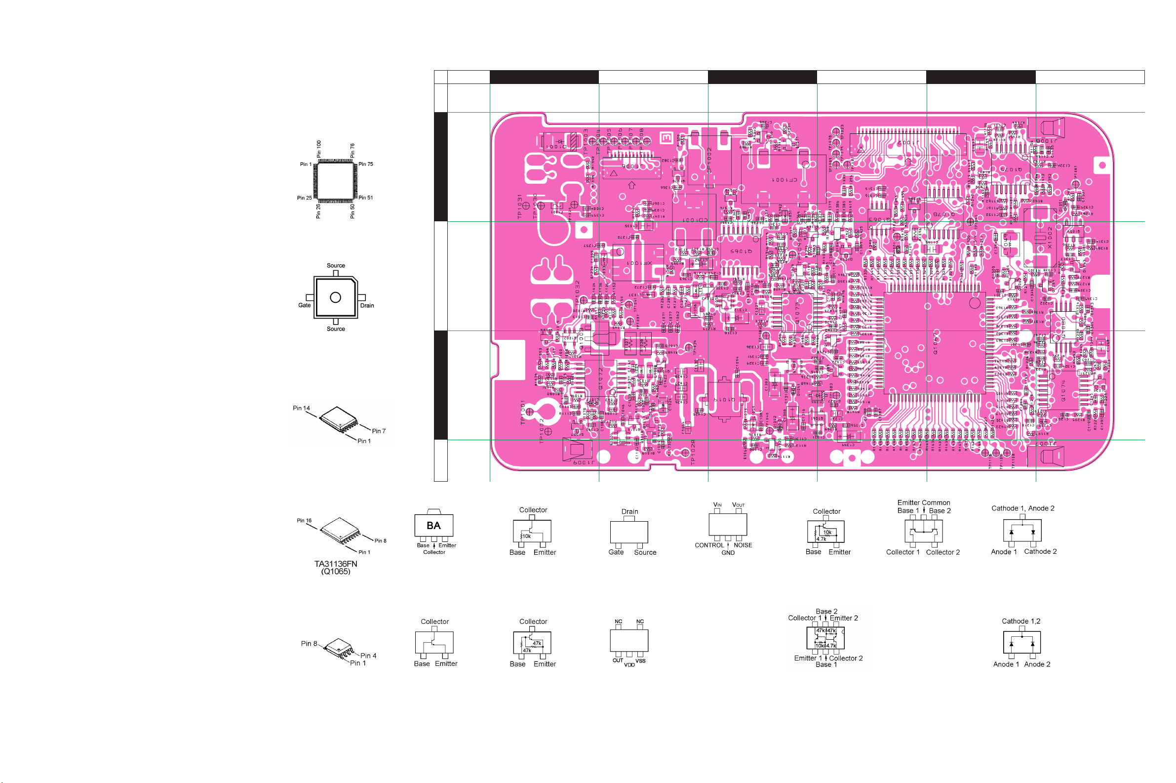
LC87FF5BP6A
(Q1067)
Main Unit (Lot. 1 ~ 2)
Parts Layout (Side A)
A B C D E F
1
2
2SK3476
(Q1019)
CD4066BPWR
(Q1078)
LM2902PWR
(Q1073, 1074, 1075)
NJM12902V
(Q1072)
3
4
2SB1132 (BA)
(Q1003)
DTC114TE (04)
(Q1010, 1025,
1062)
RTM002 (BA)
(Q1088)
TAR5S35U
(Q1060, 1061)
UNR911FJ0L (6O)
(Q1041, 1085)
XP1501 (5R)
(Q1002)
DA221 (K)
(D1026, 1042,
1043, 1049, 1050)
BR93L66RFVM
(Q1063)
LM2904PWR
(Q1080)
2SC4617 (BR)
(Q1064, 1069)
2SC5226 (R22)
(Q1056)
DTC144EE (26)
(Q1004, 1017,
1018, 1070, 1071,
1086, 1087)
S-80835CNMC
(Q1059)
UMD5N
(Q1006, 1058)
DAN222 (N)
(D1046, 1048)
17
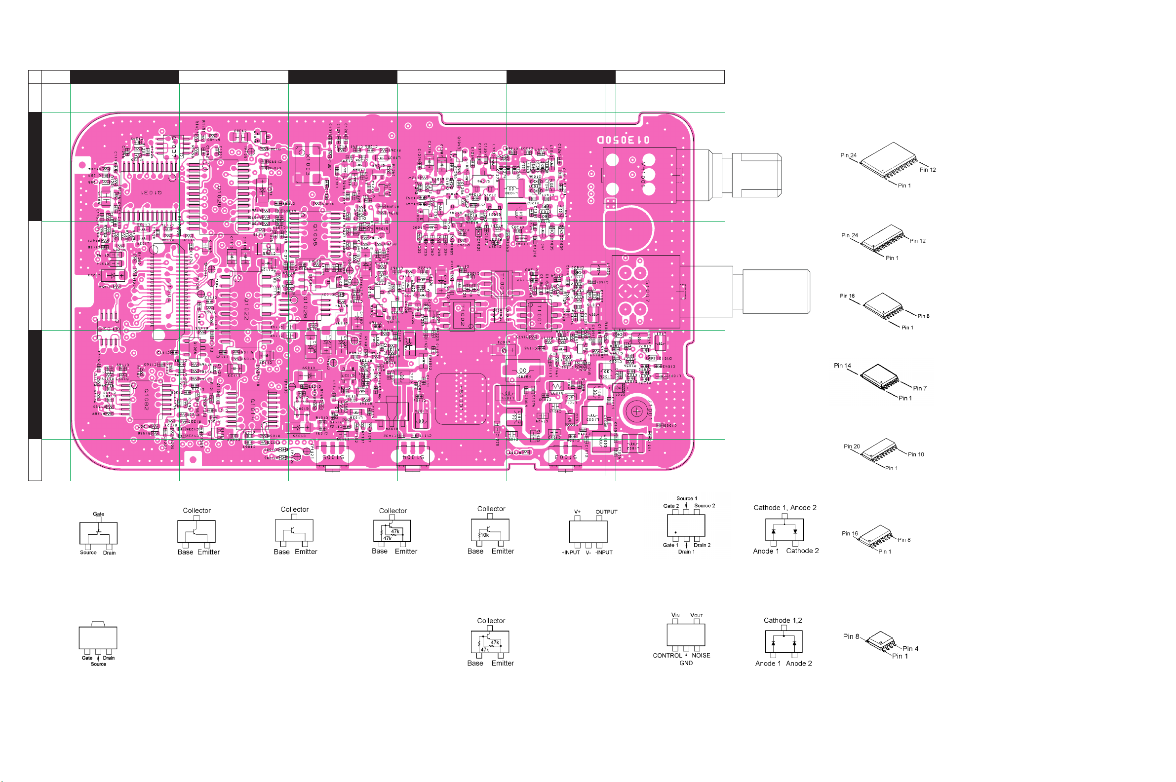
Main Unit (Lot. 1 ~ 2)
Parts Layout (Side B)
a b c d e f
1
2
AK2345
(Q1031)
M62364FP
(Q1020)
CD4053BPWR
(Q1014)
3
LM2902PWR
(Q1082)
4
SA7025DK
(Q1068)
2SK508 (K52)
(Q1046)
2SK880GR (XG)
(Q1066)
2SA1774 (FR)
(Q1035)
2SC3356 (R24)
(Q1027)
2SC4227 (R32)
(Q1051)
2SC4617 (BR)
(Q1053)
2SC5005 (73)
(Q1032, 1040, 1049)
2SC5226 (R22)
(Q1021)
DTA144EE (16)
(Q1036)
DTC114TE (04)
(Q1038, 1047,
1083)
NJM2130F
(Q1030, 1084)
SPM5001
(Q1034)
DA221 (K)
(D 1025)
LA8630M
(Q1022)
18
2SK3475
(Q1024)
DTC144EE (26)
(Q1033, 1043,
1048)
TAR5S50U
(Q1005)
DAN222 (N)
(D1023)
BD6111FV
(Q1028)
TC4W53FU
(Q1029)
TC7W74FU
(Q1037)
–8.5 dBμV emf
@485.1 MHz
RX: 7.4 V
TX: 7.1 V
RX: 7.4 V
TX: 6.7 V
RX: 5.0 V
TX: 4.3 V
RX: 5.0 V
TX: 0.1 V
SW ON: 0 V
SW OFF: 3.5 V
PWR ON: 0 V
PWR OFF: 6.7 V
RX: 0.1 V
TX: 3.4 V
RX: 0 V
TX: 0.8 V
RX: 0 V
TX: 5.0 V
PWR ON: 7.4 V
PWR OFF: 1.1 V
TX: 7.1 V
SAVE ON: 0 V
SAVE OFF: 4.9 V
TX: 0 V
7.4 V
PWR ON: 1.7 V
PWR OFF: 0 V
PWR ON: 5.0 V
PWR OFF: 0 V
RX: 0 V
TX: 5.0 V
3.5 V
–10.5 dBμV emf
@485.1 MHz
RX: 7.4 V
TX: 6.9 V
RX: 7.4 V
TX: 6.9 V
RX: 1.3 V
TX: 0 V
RX: 4.1 V
TX: 0 V
RX: 1.5 V
TX: 0 V
RX: 0.7 V
TX: 0 V
RX: 0 V
TX: 2.0 V
SAVE ON: 0 V
SAVE OFF: 3.4 V
TX: 0 V
RX: 3.0 V
TX: 0 V
RX: 7.4 V
TX: 6.9 V
RX: 3.1 V
TX: 0 V
2.5 V @25 °C
RX: 0 V
TX: 3.1 V
RX: 0 V
TX: 3.9 V
RX: 0 V
TX: 3.0 V
3.5 V
MUTE: 3.5 V
BUSY: 0.5 V
TX: 0.5 V
RX: 0 V
TX: 1.2 V
MUTE: 0 V
BUSY: 3.5 V
TX: 3.5 V
–0.2 dBμV emf
@485.1 MHz
RX: 1.6 V
TX: 0.6 V
@485.1 MHz
5.1 V
RX: 0 V
TX: 3.9 V
RX: 3.2 V
TX: 0 V
RX: 2.5 V
TX: 3.2 V
RX: –2.1 V
TX: –1.3 V
@485.1 MHz
RX: –4.9 V
TX: –5.0 V
0.1 V
RX: 0.8 V
TX: 0.9 V
RX: –1.7 V
TX: –1.0 V
@485.1 MHz
RX: –4.8 V
TX: –5.0 V
MUTE: 0 V
BUSY: 0.3 V
TX: 0 V
3.5 V
RX: –4.2 V
TX: –4.6 V
RX: 0.1 V
TX: 3.4 V
MUTE: 0 V
BUSY: 0.3 V
TX: 0 V
RX: 3.5 V
TX: –4.6 V
2.7 V
0.8 V
RX: –3.3 V
TX: 0.1 V
RX: –4.2 V
TX: 0 V
SAVE ON: 0 V
SAVE OFF: 3.5 V
RX: 3.0 V
TX: 2.0 V
RX: 0 V
TX: 5.0 V
3.5 V
SAVE ON: 3.5 V
SAVE OFF: 0.6 V
RX: 3.8 V
TX: 4.2 V
0.8 V
4.2 V
RX: 3.0 V
TX: 0 V
–3.2 dBμV emf
RX: 1.4 V
TX: 0 V
RX: 0.7 V
TX: 0 V
SAVE ON: 0 V
SAVE OFF: 4.9 V
TX: 0 V
5.0 V
4.9 V
RX: 4.2 V
TX: 3.7 V
RX: 3.0 V
TX: 2.5 V
2.7 V
0.1 V
RX: 2.9 V
TX: 0 V
RX: 2.9 V
TX: 0 V
SAVE ON: 0 V
SAVE OFF: 3.4 V
TX: 0 V
RX: 2.7 V
TX: 2.1 V
@485.1 MHz
RX: 4.9 V
TX: 0 V
RX [W]: 1.0 V
RX [N]: 1.9 V
TX [W]: 0 V
TX [N]: 1.9 V
Main Unit (Lot. 3 ~ 12)
Circuit Diagram
RX: 2.8 V
TX: 0 V
RX: 2.4 V
TX: 0 V
0 V
RX [W]: 1.0 V
RX [N]: 1.9 V
TX [W]: 0 V
TX [N]: 1.9 V
0 V
3.5 V
1.5 V
RX: 1.3 V
TX: 0 V
RX [W]: 3.6 V
RX [N]: 0.1 V
TX: 0 V
PLL LOCK: 3.4 V
PLL UNLOCK: 0 V
RX [W]: 0 V
RX [N]: 2.4 V
RX [W]: 1.5 V
RX [N]: 0 V
TX: 0 V
3.4 V
RX: 0.6 V
TX: 0 V
RX: 3.4 V
TX: 0 V
RX [W]: 0 V
RX [N]: 3.0 V
RX: 0.8 V
TX: 0 V
3.5 V
3.5 V
0.2 V p-p
RX: 3.5 V
TX: 0 V
RX: 0 V
TX: 3.4 V
MUTE: 3.1 V
BUSY: 0 V
TX: 3.1 V
3.5 V
3.5 V
OPTION ON: 0 V
OPTION OFF: 3.5 V
MUTE: 0 V
BUSY: 1.7 V
TX: 1.7 V
MUTE: 0 V
BUSY: 3.5 V
TX: 3.5 V
PWR ON: 6.7 V
PWR OFF: 7.0 V
5.1 V
7.4 V
e
3.5 V
3.5 V
c
d
3.5 V
5.7 V
PWR ON: 3.5 V
PWR OFF: 0 V
PWR ON: 3.4 V
PWR OFF: 0 V
4.1 V
PWR ON: 3.6 V
PWR OFF: 0 V
PWR ON: 7.4 V
PWR OFF: 0 V
RX: 2.7 V
TX: 0.7 V
c
PWR OFF: 3.5 V
PWR ON: 1.8 V
d
PWR OFF: 3.5 V
CLOCK SHIFT ON: 2.7 V
CLOCK SHIFT OFF: 3.4 V
e
PWR OFF: 3.5 V
PWR ON: 1.8 V
LED HI: 3.3 V
LED LOW: 0 V
LED OFF: 0 V
LED ON: 3.4 V
LED OFF: 0 V
RX: 0 V
TX: 3.5 V
RX [W]: 0 V
RX [N]: 3.3 V
RX: 3.5 V
TX: 0 V
19

Main Unit (Lot. 3 ~ 12)
Note
20
 Loading...