

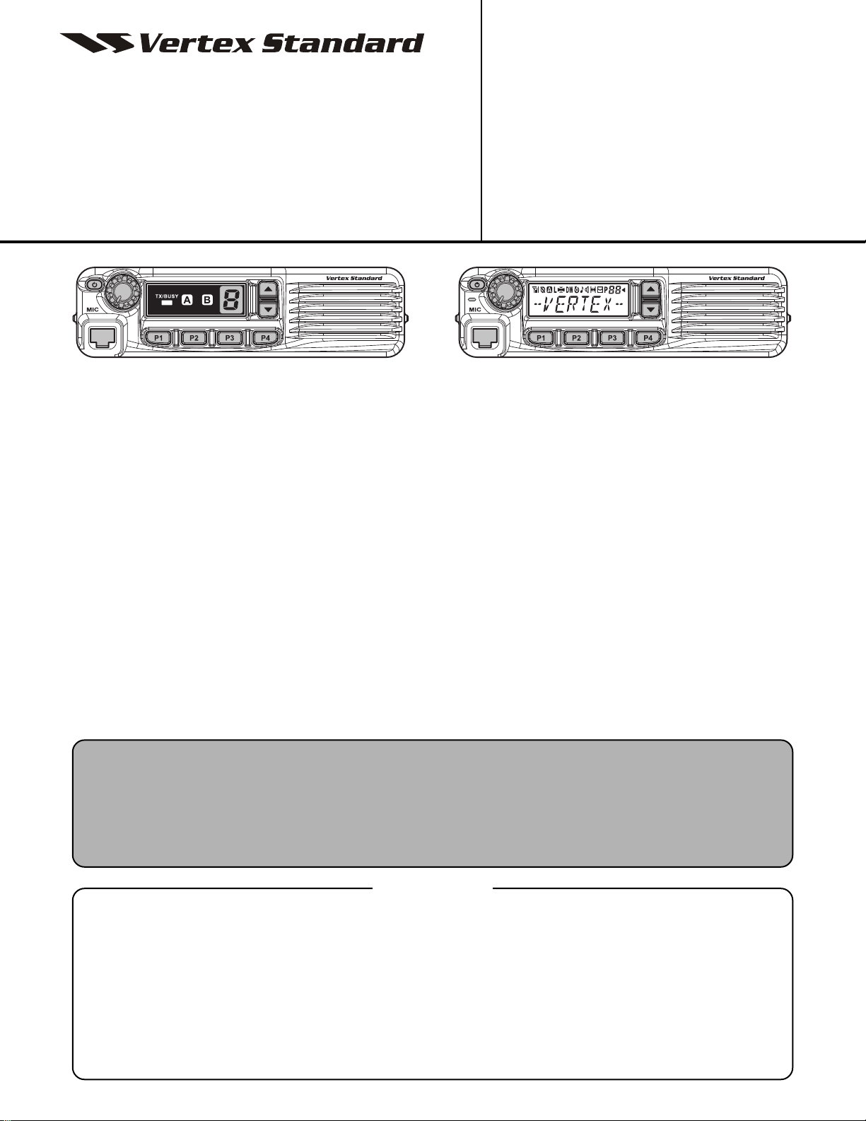
VHF FM Transceiver
VX-4500
VX-4600
Series
Series
Service Manual
2011VERTEX STANDARD CO., LTD. EC093N90B
©
VERTEX STANDARD CO., LTD.
4-8-8 Nakameguro, Meguro-Ku, Tokyo 153-8644, Japan
VERTEX STANDARD
US Headquarters
10900 Walker Street, Cypress, CA 90630, U.S.A.
YAESU UK LTD.
Unit 12, Sun Valley Business Park, Winnall Close
Winchester, Hampshire, SO23 0LB, U.K.
VERTEX STANDARD HK LTD.
Unit 1306-1308, 13F., Millennium City 2, 378 Kwun Tong Road,
Kwun Tong, Kowloon, Hong Kong
VERTEX STANDARD (AUSTRALIA) PTY., LTD.
Tally Ho Business Park, 10 Wesley Court, East Burwood, VIC, 3151
VX-4500
Series
VX-4600
Series
Introduction
This manual provides the technical information necessary for servicing the VX-4500/-4600 Series Mobile Transceiver.
Servicing this equipment requires expertise in handing surface-mount chip components. Attempts by non-qualified
persons to service this equipment may result in permanent damage not covered by the warranty, and may be illegal
in some countries.
Two PCB layout diagrams are provided for each double-sided board in this transceiver. Each side of the board is
referred to by the type of the majority of components installed on that side (“Side A” or “Side B”). In most cases one
side has only chip components (surface-mount devices), and the other has either a mixture of both chip and leaded
components (trimmers, coils, electrolytic capacitors, ICs, etc.), or leaded components only.
As described in the pages to follow, the advanced microprocessor design of the VX-4500/-4600 allows a complete
alignment of this transceiver to be performed without opening the case of the radio; all adjustments can be performed
from the personal computer, using with the Vertex Standard FIF-10A USB Programming Interface and CE115 Software.
While we believe the information in this manual to be correct, Vertex Standard assumes no liability for damage that
may occur as a result of typographical or other errors that may be present. Your cooperation in pointing out any
inconsistencies in the technical information would be appreciated.
Important Note
The VX-4500/-4600 was assembled using Pb (lead) free solder, based on the RoHS specification.
Only lead-free solder (Alloy Composition: Sn-3.0Ag-0.5Cu) should be used for repairs performed on this apparatus. The
solder stated above utilizes the alloy composition required for compliance with the lead-free specification, and any solder
with the above alloy composition may be used.
Contents
Specifications ............................................................... 2
DSUB 15-pin Accessory Connector .......................... 3
Exploded View & Miscellaneous Parts ................... 4
Block Diagram.............................................................. 5
Circuit Description ...................................................... 6
Alignment ..................................................................... 8
Installation of Option ............................................... 22
Board Units (Schematics, Layouts & Parts)
MAIN Unit ............................................................. 23
FRONT-A Unit (VX-4500).................................... 30
FRONT-B Unit (VX-4600).................................... 37
Optional Units (Schematics, Layouts & Parts)
DVS-8 Voice Storage Unit .................................... 44

Specifications
General
Frequency Ranges: 134 -174 MHz
Number of Channels: 8 channels (VX-4500 Series)
Power Supply Voltage: 13.6 V ± 20 %
Channel Spacing: 12.5/20/25 kHz
Pll Steps: 1.25/2.5/5/6.25 kHz
Current Consumption (@13.6 V): 11 A (TX: 50 W), 6 A (TX: 25 W)
Operating Temperature Range: –22 °F to +140 °F (–30 °C to +60 °C)
Frequency Stability: ±2.5 ppm (–22 °F to +140 °C [–30 °C to +60 °C])
Antenna Impedance: 50 Ohms
Dimension (W x H x D): 6.5" x 1.8" x 6.1" inch (165 x 45 x 155 mm) (W/O knob)
Weight (Approx.): 2.8 lbs (1.25 kg)
Receiver: measured by TIA/EIA-603
Circuit Type: Double-conversion Superheterodyne
Intermediate Frequency: 1st: 50.85 MHz, 2nd: 450 kHz
Sensitivity (12 dB SINAD): 0.25 μV
Adjacent Channel Selectivity: 70 dB (12.5 kHz)
Hum & Noise: 40 dB (12.5 kHz)
Intermodulation: 75 dB
Spurious & Image Rejection: 80 dB
Audio Output: Internal: 4 W @20 Ohms, 5% THD
512 channels with 32 groups (VX-4600 Series)
2.5 A (RX)
200 mA (RX: SQL Closed)
75 dB (25 kHz)
45 dB (25 kHz)
External: 12 W @4 Ohms, 5% THD
Transmitter: measured by TIA/EIA-603
Modulation Type: Variable Reactance
Output Power (selectable): 50/25/12.5/5 W
Emission Type: 16K0F3E, 11K0F3E
Maximum Deviation: ±2.5 kHz (12.5 kHz)
FM Hum & Noise: 40 dB (12.5 kHz)
Audio Distortion: < 3 % (@1 kHz)
Conducted Spurious Emission: 70 dB below Carrier
±5 kHz (25 kHz)
45 dB (25 kHz)
Receiver: measured by EN 300 086
Circuit Type: Double-conversion Superheterodyne
Intermediate Frequency: 1st: 50.85 MHz, 2nd: 450 kHz
Sensitivity (20 dB SINAD): -5 dBμ/-2dBμ (25 kHz/12.5 kHz)
Adjacent Channel Selectivity: 70 dB (12.5 kHz)
Hum & Noise: 40 dB (12.5 kHz)
Intermodulation: 70 dB
Spurious & Image Rejection: 85 dB
Audio Output: Internal: 4 W @20 Ohms, 5% THD
75 dB (25 kHz)
45 dB (25 kHz)
External: 12 W @4 Ohms, 5% THD
Transmitter: measured by EN 300 086
Modulation Type: Variable Reactance
Output Power (selectable): 25/12.5/5/1 W
Emission Type: 16K0F3E, 11K0F3E
Maximum Deviation: ±2.5 kHz (12.5 kHz)
FM Hum & Noise: 40 dB (12.5 kHz)
Audio Distortion: < 3 % (@1 kHz)
Conducted Spurious Emission: < -36 dBm@
±5 kHz (25 kHz)
45 dB (25 kHz)
<
1 GHz, -30 dBm>@1 GHz
=
Specifications subject to change without notice or obligation.
2VX-4500/-4600 Series VHF FM Transceiver Service Manual
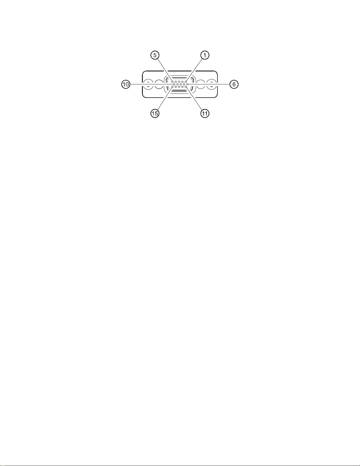
DSUB 15-pin Accessory Connector
Pin 1: AF IN (ANALOG INPUT
External Microphone Input. Nominal input level is
4 mV (or -10 dBm; programmed via the CE115 programmer) at 600-ohm.
Pin 2: AF OUT (ANALOG OUTPUT
Low-level receiver output. Peak signal level is -10 dBm
at 600-ohm.
)
)
Pin 3: AF GND
Ground for all logic levels and power supply return.
Pin 4: DC OUT (13.6 V DC OUTPUT
Switched 13.6V output for supplying power to an accessory.
Maximum output current is 1 A.
Pin 5: RSSI (ANALOG OUTPUT
A DC voltage proportional to the strength of the signal currently being received (Receiver Signal Strength
Indicator) is provided on this pin. This low impedance
output is gererated by the receiver IF sub-system and
bufferd by an internal op-amp. Typical output voltages are 1 V (@No Signal Input) through 2.5 V (@50 dB
Signal Input).
)
)
Pin 6: EXT PTT
Shorting this port to ground causes the transceiver to
be placed in the Transmit mode, while opening the
connection to this port returns the transceiver to the
Receive mode. Opening voltage is 5 V, closed current
approx. 5 mA.
Pin 7: TRX
This port is intended for controlling an external TX/
RX switching circuit. When the transceiver is placed
in the Receiver mode, this port is 5 V. When the transceiver is placed in the Transmit mode, this port reduce
to 0 V.
This port is open drain output which can sink approx.
50 mA when active.
Pin 8: ING (IGNITION SENSE FEATURE
The VX-4500/-4600 may be automatically be switched
to the STND-BY mode when the vehicle's ignition key
is turned on. Maximum current is 20 mA.
)
Pin 9 - 12: ACC1 - ACC4 (ACCESSORY POR T)
These output port features can be programmed via the
CE115 programmer. Each port is open drain output
which can sink approx. 50 mA when active.
Pin 13: Not Used
Pin 14: Not Used
Pin 15: GND
Chassis ground
3VX-4500/-4600 Series VHF FM Transceiver Service Manual
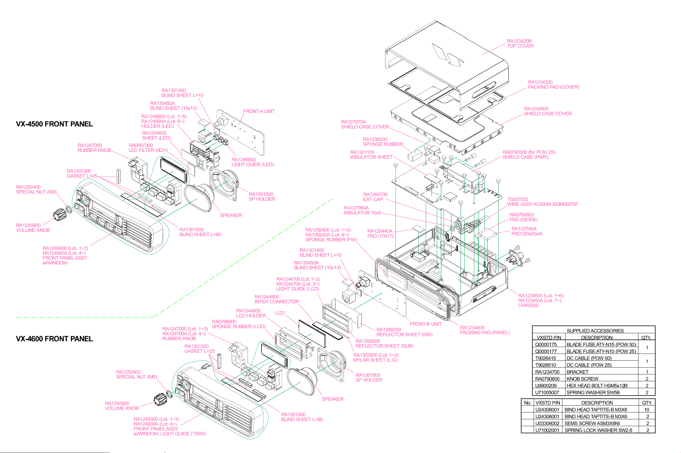
Exploded View & Miscellaneous Parts
Non-designated parts are available only as
part of a designated assembly.
4VX-4500/-4600 Series VHF FM Transceiver Service Manual
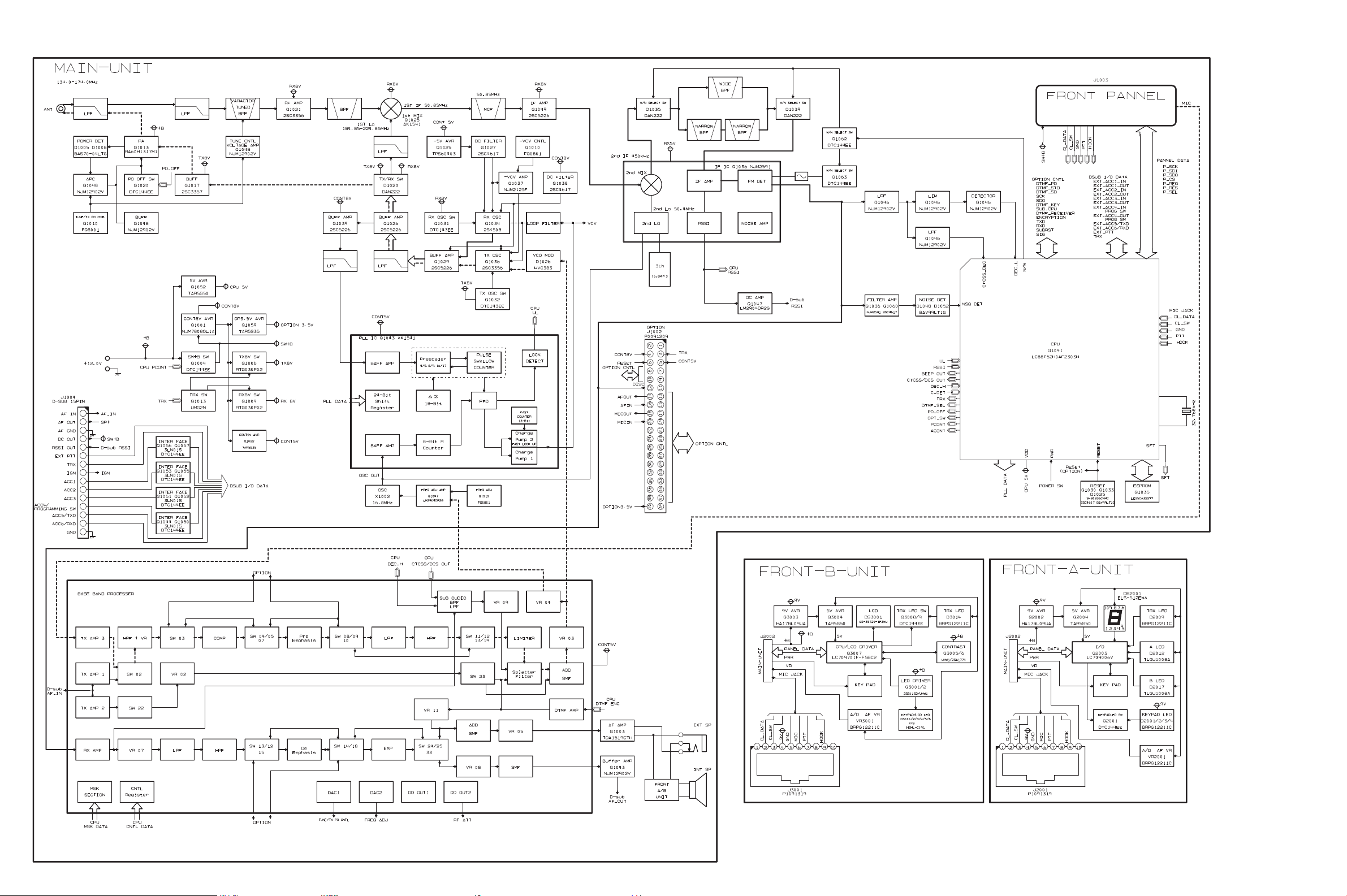
Block Diagram
VX-4500/-4600 Series VHF FM Transceiver Service Manual
5

Circuit Description
1. Circuit Configuration by Frequency
The receiver is a double-conversion superheterodyne with a first
intermediate frequency (IF) of 50.85 MHz and a second IF of
450 kHz. Incoming signal from the antenna is mixed with the
local signal from the VCO/PLL to produce the first IF of 50.85
MHz. This is then mixed with the 50.4 MHz second local oscillator output to produce the 450 kHz second IF. This is detected
to give the demodulated signal. The transmit signal frequency
is generated by the PLL VCO and modulated by the signal from
the microphone. It is then amplified and sent to the antenna.
2. Receiver System
2-1. Front-end RF amplifier
Incoming RF signal from the antenna is delivered to the RF
Unit and passes through the Low-pass filter, Undesired frequencies are removed by the varactor diode tuned band-pass filter
consisting of diodes D1013, D1015, D1022, & D1023 (all
HVC327C) and Coils L1012 & L1013, and capacitors C1090,
C1095, C1105, C1107, C1116, & C1117. The passed signal is
amplified by Q1021 (2SC3356) and moreover cuts animage
frequency with the band pass filter consisting of Coils L1012,
L1015, L1018, & L1033, and capacitors C1130, C1135, C1 151,
C1156, C1 173, C1181, C1 182, C1 197, C1205, C1217, & C1233.
The filtered RF signal is then delivered to the first Mixer.
2-2. First Mixer
The 1st mixer consists of Q1040 (AK1220). Buffered output
from the VCO is amplified by Q1026 (2SC5226) to provide a
pure first local signal between 184.85 and 224.85 MHz for injection to the first mixer. The output IF signal is sent to the
crystal filter. The IF signal then passes through monolithic crystal
filter XF1001 (± 5.5 kHz BW) to strip away all but the desired
signal.
2-3. IF Amplifier
The first IF signal is amplified by Q1049 (2SC5226). The
amplified first IF signal is applied to FM IF subsystem IC Q1054
(NJM2591V) which contains the second mixer, second local
oscillator, limiter amplifier, noise amplifier, and S-meter amplifier. The signal from reference oscillator X1002 is multiplied
3 times in Q1054 (NJM2591V). It is mixed with the first IF
signal and becomes the second IF signal of 450 kHz. The second IF then passes through the ceramic filter CF1002 (for wide
channels) or CF1001 and CF1003 (for narrow channels) to strip
away unwanted mixer products and remove amplitude variations in the 450 kHz IF before detection of the speech by the
ceramic discriminator CD1001.
2-4. Audio amplifier
Detected signal from Q1054 (NJM2591V) is delivered to
Q1010 (FQ0801) and is output by Q1010 (FQ0801) pin 17
through the band pass filter. When the optional unit is installed,
Q1010 (FQ0801) is made "OFF" and the AF signal from Q1010
(FQ0801) pin 21 goes to the optional unit and returns to Q1010
(FQ0801) pin 20 from the optional unit. When the optional
unit is not installed, Q1010 (FQ0801) is made "ON" and the
signal goes through Q1010 (FQ0801) pin 20/21. The signal is
stored in the AF volume via AF mute and the de-emphasis inside Q1010 (FQ0801). The AF volume is controlling Q1010
(FQ0801) by the CPU. After that, it enters AF power amplifier
Q1003 (TDA1519CTH) after passing AF volume. The output
of Q1003 (TDA1519CTH) drives a speaker (it chooses the
external SP or internal SP in J1001).
2-5. Squelch Circuit
There are 16 levels of squelch setting from 0 to 15. The level 0
means open squelch. The level 1 means the threshold setting
Level and level 15 means tight squelch. From 1 to 14 is established in the middle of threshold and tight. The bigger figure is
nearer the tight setting. The level 16 becomes setting of carrier
squelch.
2-5-1. Noise Squelch
The noise squelch circuit is composed of the band pass filter of
Q1054 (NJM2591V), noise amplifier Q1060 (2SC4617), and
noise detector D1048, D1052 (both DA221). When a carrier
isn't received, the noise ingredient which goes out of the demodulator Q1054 (NJM2591V) is amplified in Q1060
(2SC4617) through the band pass filter Q1054 (NJM2591V),
is detected to DC voltage with D1048 and D1052 (both DA221),
and is inputted to pin 15 the A/D port of the Q1041
(LC88F52H0A) CPU. When a carrier is received, the DC voltage becomes "LOW" because the noise is compressed. When
the detected voltage to CPU is "HIGH", the CPU stops AF output with Q1010 (FQ0801) "OFF". When the detected voltage
is low, the CPU makes Q1010 (FQ0801) "ON" and the AF
signal is output.
2-5-2. Carrier Squelch
Pin 14 (A/D port) of Q1047 (NJM2904V) CPU detects RSSI
voltage output from pin 12 of Q1054 (NJM2591V), and con-
trols AF output. The RSSI output voltage changes according to
the signal strength of carrier. The stronger signal causes the
RSSI voltage to be higher voltage. The process of the AF signal
control is the same as Noise Squelch. The shipping data is adjusted 3 dB higher than squelch tight sensitivity.
6VX-4500/-4600 Series VHF FM Transceiver Service Manual

Circuit Description
3. Transmitter System
3-1. Mic Amplifier
The AF signal from microphone jack J2001 (VX-4500) or J3001
(VX-4600) is amplified with microphone amplifier in Q1010
(FQ0801), is amplified a second time after microphone selection switch Q1010 (FQ0801), and passes through microphone
gain volume in Q1010 (FQ0801). The control from the CPU
passes output and it passes a pre-emphasis circuit. When an
option unit is installed, the AF signal from Q1010 (FQ0801)
pin 38 goes through the option unit, and returns to Q1010
(FQ0801) pin 39. When an option unit isn't installed, Q1010
(FQ0801) is inputted to the pre-emphasis circuit. The signal
passes the limiter and splatter filter of Q1010 (FQ0801), and
is adjusted by maximum deviation adjustment volume. The adjusted low frequency signal ingredient is amplified by Q1047
(NJM2904V), added modulation terminal of TCXO (X1002),
the FM modulation is made by reference oscillator.
The high frequency signal ingredient is amplified, and adjusted
the level by volume Q1010 (FQ0801) to make frequency bal-
ance between low frequency. After that, it is made FM modulation to transmit carrier by the modulator D1026 (HVC383B)
of VCO.
3-2. Drive and Final amplifier
The modulated signal from the VCO Q1034 (2SK508) is buff-
ered by Q1026 (2SC5226) and amplified by Q1017
(2SC3356). The low-level transmit signal is then applied to
the Power Module Q1013 (RA60H1317M1A: for 50 W,
RA30H1317M1: for 25 W) for final amplification up to 50 or
25 watts output power. The transmit signal is then low-pass
filtered to suppress away harmonic spurious radiation before
delivery to the antenna.
3-3. Automatic Transmit Power Control
The output power of Power Module is detected by CM coupler,
it is detected by D1005 & D1008 (both HSM88AS) and is in-
put to comparator Q1048 (NJM12902V). The comparator com-
pares two different voltages and makes output power stable by
controlling the bias voltage of the Power Module. There are 4
levels of output power (Hi, Lo3, Lo2 and Lo1) it is switched by
the Voltage of Q1010 (FQ0801) pin 44.
3-4. PLL Frequency Synthesizer
The frequency synthesizer consists of PLL IC Q1043
(AK1541), VCO, TCXO (X1002) and buffer amplifier. The
output frequency from TCXO is 16.8 MHz and the tolerance is
± 2.5 ppm (in the temperature range –22 °F to +140 °F [–30 °C
to +60 °C]).
3-4-1. VCO
While the radio is receiving, the RX oscillator Q1034 (2SK508)
in VCO generates a programmed frequency between 184.85
and 224.85 MHz as 1st local signal. While the radio is transmitting, the TX oscillator Q1036 (2SC3356) in VCO generates a
frequency between 134 and 174 MHz. The output from the oscillator is amplified by buffer amplifier Q1029 (2SC5226) and
becomes output of VCO. The output from the VCO is divided,
one is amplified by Q1039 (2SC5226) and feed back to pin 17
of the PLL IC Q1043 (AK1541). It is amplified about the RF
signal Q1029 (2SC5226) which was made by VCO. RF
changes with the carrier signal of the transmitter and the mixer
local signal of the receiver with D1020 (DAN222).
3-4-2. VCV CNTL
Tuning voltage (VCV) of the VCO is expanding the lock range
of VCO by controlling of the varactor diode at the voltage and
the control voltage from PLL IC Q1043 (AK1541). As for the
control voltage adjustment by the varactor diode, it controls the
negative voltage to make with Q1025 (TPS60303) with the
D/A converter inside Q1010 (FQ0801) and Q1037
(NJM2125F), it has the anode potential of the varactor diode
variably.
3-4-3. PLL
The PLL IC Q1043 (AK1541) consists of reference divider,
main divider, phase detector, charge pumps and delta sigmafractional accumulator. The reference frequency from TCXO is
inputted to pin 10 of PLL IC Q1043 (AK1541) and is divided
by reference divider. This IC is decimal point dividing PLL IC
Q1043 (AK1541) and the dividing ratio becomes 1/8 of usual
PLL frequency step. Therefore, the output of the reference divider is 8 times the frequency of the channel step. For example
when the channel stepping is 5 kHz, the output of reference
divider becomes 40 kHz. On the other hand, inputted feed back
signal to pin 17 of PLL IC Q1043 (AK1541 ) from VCO is
divided with the dividing ratio which becomes the same frequency as the output of reference divider. These two signals are
compared by the phase detector, and the phase difference pulse
is generated. The phase difference pulse and the pulse from
fractional accumulator pass through the charge pumps and LPF.
It becomes the DC voltage (VCV) to control the VCO. The
oscillation frequency of VCO is locked by the control of this
DC voltage. The PLL serial data from CPU Q1041
(LC88F52H0A) is sent with three lines of SDO (pin 20), SCK
(pin 22) and PSTB (pin 45). The lock condition of PLL is output from the UL (pin 18) terminal and UL becomes "H" at the
time of the lock condition and becomes "L" at the time of the
unlocked condition. The CPU Q1041 (LC88F52H0A) always
watches over the UL condition, and when it becomes "L" unlocked condition, the CPU Q1041 (LC88F52H0A) prohibits
transmitting and receiving.
7VX-4500/-4600 Series VHF FM Transceiver Service Manual

Alignment
Introduction
The VX-4500/-4600 series has been aligned at the factory
for the specified performance across the entire frequency
range specified. Realignment should therefore not be necessary except in the event of a component failure. All component replacement and service should be performed only
by an authorized Vertex Standard representative, or the
warranty policy may be voided.
The following procedures cover the sometimes critical and
tedious adjustments that are not normally required once
the transceiver has left the factory. However, if damage
occurs and some parts are replaced, realignment may be
required. If a sudden problem occurs during normal operation, it is likely due to component failure; realignment
should not be done until after the faulty component has
been replaced.
We recommend that servicing be performed only by authorized Vertex Standard service technicians who are experienced with the circuitry and fully equipped for repair
and alignment. Therefore, if a fault is suspected, contact
the dealer from whom the transceiver was purchased for
instructions regarding repair. Authorized Vertex Standard
service technicians realign all circuits and make complete
performance checks to ensure compliance with factory
specifications after replacing any faulty components.
Those who do undertake any of the following alignments
are cautioned to proceed at their own risk. Problems
caused by unauthorized attempts at realignment are not
covered by the warranty policy. Also, Vertex Standard
must reserve the right to change circuits and alignment
procedures in the interest of improved performance, without notifying owners. Under no circumstances should any
alignment be attempted unless the normal function and
operation of the transceiver are clearly understood, the
cause of the malfunction has been clearly pinpointed and
any faulty components replaced, and the need for realignment determined to be absolutely necessary. The following test equipment (and thorough familiarity with its correct use) is necessary for complete realignment. Correction of problems caused by misalignment resulting from
use of improper test equipment is not covered under the
warranty policy. While most steps do not require all of
the equipment listed, the interactions of some adjustments
may require that more complex adjustments be performed
afterwards. Do not attempt to perform only a single step
unless it is clearly isolated electrically from all other steps.
Have all test equipment ready before beginning, and follow all of the steps in a section in the order presented.
Required Test Equipment
Radio Tester with calibrated output level at 200 MHz
In-line Wattmeter with 5% accuracy at 200 MHz
50-ohm, 50-W RF Dummy Load
Regulated DC Power Supply (standard 13.6V DC, 15A)
Frequency Counter: ±0.2 ppm accuracy at 200 MHz
AF Signal Generator
AC Voltmeter
DC Voltmeter
VHF Sampling Coupler
Microsoft® Windows® 2000, XP, Vista or Windows7
Vertex Standard FIF-10A USB Programming Interface
and CT-104A PC Programming Cable or VPL-1 cable.
Vertex Standard CE115 PC Programming Software
Alignment Preparation & Precautions
A 50-ohm RF Dummy load and in-line wattmeter must
be connected to the main antenna jack in all procedures
that call for transmission, except where specified otherwise. Correct alignment is not possible with an antenna.
Beacuse of the BTL (Bridged Trans Less) Amplifier circuit used in the VX-4500/-4600, do not connect either side
of the speaker leads to chassis "ground."
After completing one step, read the following step to determine whether the same test equipment will be required.
If not, remove the test equipment (except dummy load
and wattmeter, if connected) before proceeding.
Correct alignment requires that the ambient temperature
be the same as that of the transceiver and test equipment,
and that this temperature be held constant between 20 °C
and 30 °C (68 °F ~ 86 °F). When the transceiver is brought
into the shop from hot or cold air, it should be allowed
time to come to room temperature before alignment.
Whenever possible, alignments should be made with oscillator shields and circuit boards firmly affixed in place.
Also, the test equipment must be thoroughly warmed up
before beginning.
Note: Signal levels in dB referred to in this procedure are
based on 0 dBμ EMF = 1.0 μV.
8VX-4500/-4600 Series VHF FM Transceiver Service Manual
Alignment
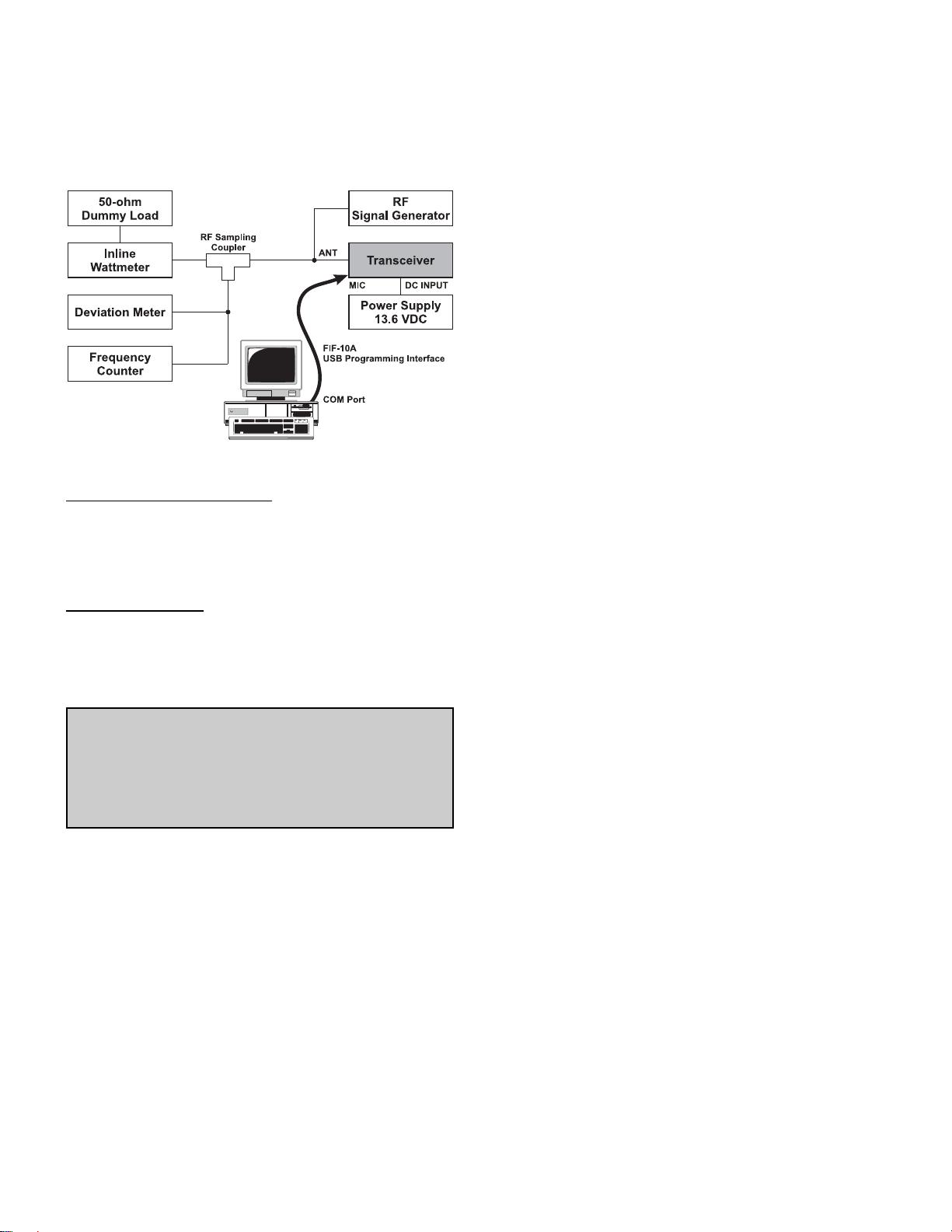
Test Setup
Setup the test equipment as shown for transceiver alignment, apply 13.6V DC power to the transceiver. Refer to
the drawings below for Alignment Points.
The Alignment T ool Outline
Installation of the alignment tool
Install the CE115 (PC Programming Software) to your
PC.
“Alignment“ function in the “Radio“ menu tab of
CE115.
Action of the switches
When the transceiver is in the “Alignment mode,“ the
action of the PTT and all PF KEYS are ignored. All of the
action is controlled by the PC.
Caution!
Please never turn off the power supply during
alignment. If the power supply is turned off during alignment, the alignment data will be corrupted.
9VX-4500/-4600 Series VHF FM Transceiver Service Manual

Alignment
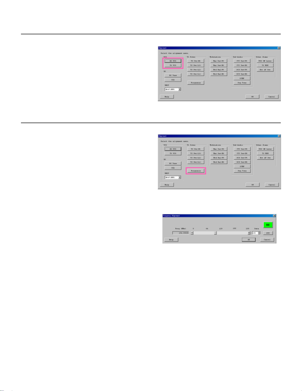
Alignment Mode
The Alignment mode allows you to align the entire radio.
The value of each parameter can be changed to the desired value by use of the “” / “” and up/down arrow
keys, along with direct number input and dragging of the
PC mouse.
To enter the Alignment Mode, select “Alignment” in the
main “Radio” menu. It will start to “Upload” the alignment data from the radio to the PC. Pressing the “OK”
button will then "Download" the alignment data to the
radio and exit the Alignment Mode.
Note: when all items are to be aligned, it is strongly recommended to align them according to the following sequence. Detailed information for each step may be found
in the “Help” file within CE115 (PC Programming Software).
1. VCO (Please do not adjust it)
2. PLL Reference Frequency (Frequency)
3. RX Sensitivity (RX Tune)
4. Squelch (SQL/RSSI)
5. TX Power <High/Low3/Low2/Low1>
6. Maximum Deviation <Wide/Narrow>
Please adjust the following items when needed.
Modulation Balance <Wide/Narrow>
CTCSS Deviation <Wide/Narrow>
DCS Deviation <Wide/Narrow>
DTMF Alignment
Seq Tone
VOX ON Level
TX MSK
Ext AF Out
Unit
During alignment, you may select the value among
dBμV,μV (EMF or PD), or dBm.
When performing the “RX Tune” and “SQL” alignment, the RF level shows this unit according to this
setting.
10VX-4500/-4600 Series VHF FM Transceiver Service Manual
Alignment
1. VCO (RX VCO/TX VCO) - Normally there is no need to adjust this parameter -
This parameter is to align the VCO Voltage adjustment.
2. PLL Reference Frequency (Frequency
This parameter is to align the reference frequency for PLL.
1. Press the “Frequency” button to start the alignment.
The Frequency Alignment window will appear.
2. Click the “PTT” button or press the “SPACE” bar, and
the radio will start to transmit on the center frequency
channel.
3. Set the value to get the desired frequency by dragging
the slide bar, clicking the up-down button, pressing
the left or right arrow key, or entering the value in the
entry box.
4. After getting the desired frequency click the “PTT”
button or press the “SPACE” bar to stop transmitting.
5. Click the “OK” button to finish the frequency alignment and save the data.
)
11VX-4500/-4600 Series VHF FM Transceiver Service Manual
Alignment
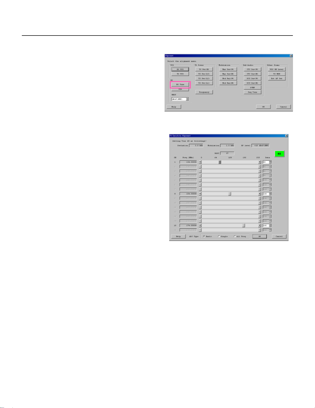
3. RX Sensitivity (RX Tune)
This parameter is to align the RX BPF (Band Pass Filter) for Receive (RX) sensitivity. The PLL Reference Frequency
(Frequency) alignment must be done before this alignment is performed.
1. Press the “RX Tune” button to start the alignment. The
RX Sensitivity Alignment window will appear.
2. Click the left mouse button on the slide bar or press
the Up / Down arrow keys, to switch to the desired
channel for alignment.
3. Set the Signal Generator according to the indication at
the top of the screen (Setting Your SG as followings).
4. Drag the slide bar, click the up-down buttons, press
the left or right arrow key, or enter the value in the
entry box to get the best RX sensitivity (Highest RSSI
value) on the selected channel.
5. Click the “OK” button to finish the RX Sensitivity alignment and save the data.
ADJ Type
Basic: “Low-edge / band center / high-edge“ and
select the channel for alignment (Default).
Single : Alignment value changes only on the se-
lected channel.
All Freq : Alignment value changes on all channels.
12VX-4500/-4600 Series VHF FM Transceiver Service Manual
Alignment
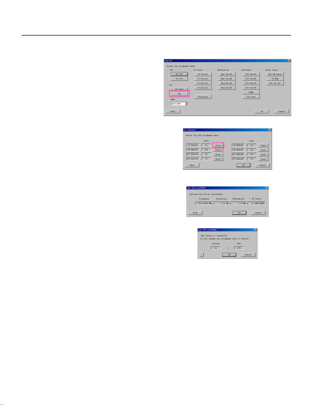
4. Squelch (SQL)
This parameter is to align the SQL (Squelch) Sensitivity.
There are several alignments as follows in the Squelch Sensitivity.
Tight SQL Level (TI NSQ W/N)
The Alignment for the Noise SQL Tight level at Wide (5k/
4k) or Narrow (2.5k).
Threshold SQL Level (TH NSQ W/N)
The Alignment for the Noise SQL Threshold level at Wide
(5k/4k) or Narrow (2.5k).
Tight SQL RSSI Level (TI RSSI W/N)
The Alignment for the “level 14” of the RSSI SQL level at
Wide (5k/4k) or Narrow (2.5k).
TX Save RSSI Level (TX SAVE W/N)
The Alignment for the TX Save RSSI level at Wide (5k/4k)
or Narrow (2.5k).
The procedure for all the alignments is as follows.
1. Click the “Start” button to open the alignment window in the SQL/RSSI Alignment menu.
2. The Alignment window will appear, Set the Signal
Generator according to the indication, then click the
“Start” button.
3. The automatic alignment will start to get the SQL or
RSSI level.
4. It will show the alignment result in the “New” box.
5. Click the “OK” button, then the data will be saved and
the alignment is finished.
13VX-4500/-4600 Series VHF FM Transceiver Service Manual
Alignment
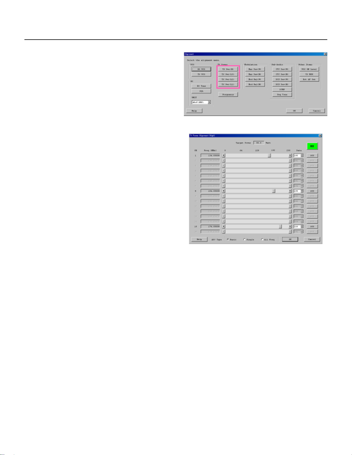
5. TX Power
This parameter is to align the “Power High”, “Power Low3”, “Power Low2” or “Power Low1” for the selected channel.
1. Press the “TX Pwr(H / L3 / L2 / L1)” button to start the
alignment. The TX Power Alignment window will
appear.
2. Click the left mouse button on the slide bar or press
the Up / Down arrow key, to select the desired channel.
3. Click the “PTT” button or press the “SPACE” bar at
the desired channel, then the radio starts to transmit
on the selected channel.
4. Set the value to get desired output power on the Power Meter by dragging the slide bar, clicking the updown button, pressing the left or right arrow key, or
entering the value in the entry box on the selected channel.
5. After getting the desired output power click the “PTT”
button or press the “SPACE” bar to stop transmitting.
6. Click the “OK” button to finish the TX Power alignment and save the data.
ADJ Type
Basic: “Low-edge / band center / high-edge“ and
select the channel for alignment (Default).
Single : Alignment value changes only on the se-
lected channel.
All Freq : Alignment value changes on all channels.
14VX-4500/-4600 Series VHF FM Transceiver Service Manual
 Loading...