

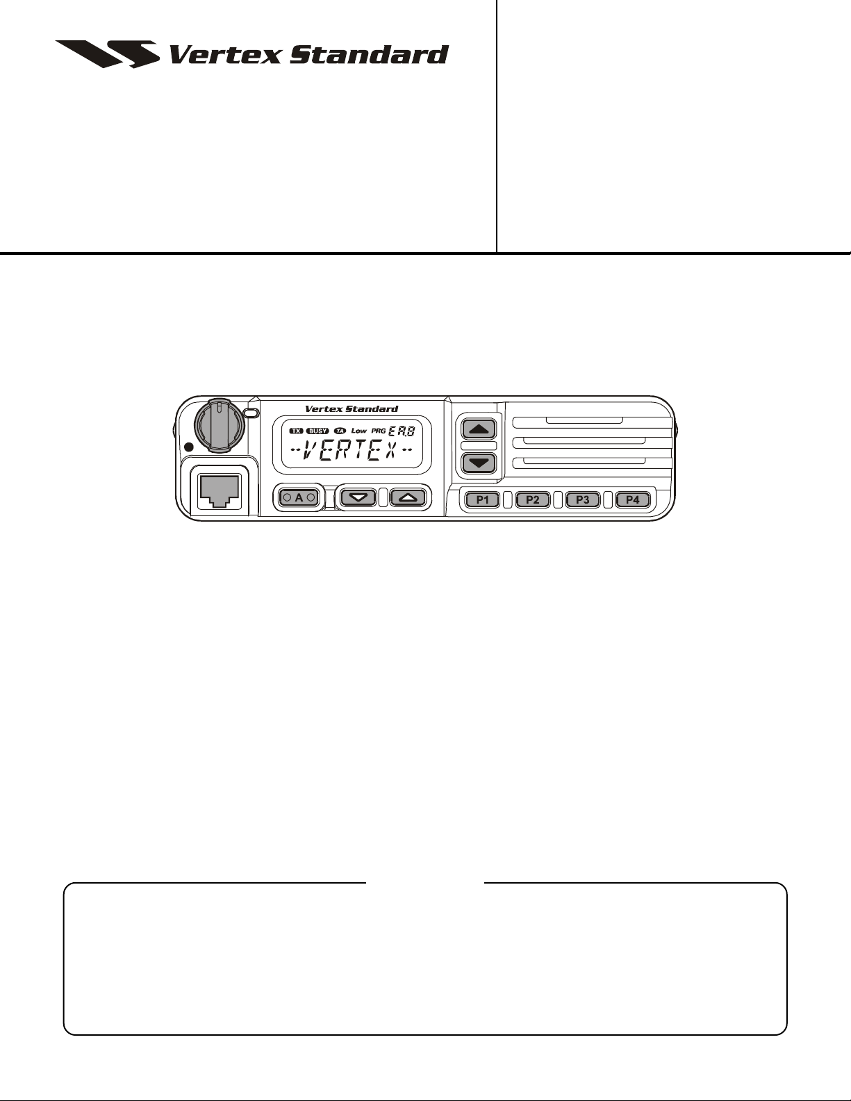
UHF FM Transceiver
VX-3200U
Service Manual
2003 VERTEX STANDARD CO., LTD. (EC039U90A)
©
VERTEX STANDARD CO., LTD.
4-8-8 Nakameguro, Meguro-Ku, Tokyo 153-8644, Japan
VERTEX STANDARD
US Headquarters
10900 Walker Street, Cypress, CA 90630, U.S.A.
YAESU EUROPE B.V.
P.O. Box 75525, 1118 ZN Schiphol, The Netherlands
YAESU UK LTD.
Unit 12, Sun Valley Business Park, Winnall Close
Winchester, Hampshire, SO23 0LB, U.K.
VERTEX STANDARD HK LTD.
Unit 5, 20/F., Seaview Centre, 139-141 Hoi Bun Road,
Kwun Tong, Kowloon, Hong Kong
Introduction
This manual provides technical information necessary for servicing the VX-3200U Transceiver.
Servicing this equipment requires expertise in handling surface-mount chip components. Attempts by non-qualified
persons to service this equipment may result in permanent damage not covered by the warranty, and may be illegal in
some countries.
Two PCB layout diagrams are provided for each double-sided circuit board in the transceiver. Each side of thr board is
referred to by the type of the majority of components installed on that side (“leaded” or “chip-only”). In most cases one
side has only chip components, and the other has either a mixture of both chip and leaded components (trimmers, coils,
electrolytic capacitors, ICs, etc.), or leaded components only.
While we believe the technical information in this manual to be correct, Vertex Standard assumes no liability for damage
that may occur as a result of typographical or other errors that may be present. Your cooperation in pointing out any
inconsistencies in the technical information would be appreciated.
Contents
Specifications ..................................................... 2
DSUB 9-pin Accessory Connector.................. 3
Exploded View & Miscellaneous Parts ......... 4
Block Diagram ................................................... 5
Interconnection Diagram .................................7
Circuit Description .........................................9
Alignment ......................................................11
Board Unit (Schematics, Layouts & Parts)
RF Unit .......................................................................... 17
Panel Unit ..................................................................... 31
1

Specifications
General
Frequency range: 400-430 MHz (Version A)
450-490 MHz (Version D)
480-512 MHz (Version F)
Number of Groups: 10
Number of Channels : 128 channels
PLL Steps: 5.0 kHz/6.25kHz
Power Supply Voltage: 13.6V DC ±15 %
Channel Spacing: 12.5 / 25.0 kHz
Current Consumption (Approx.): TX: 10 A
RX: 700 mA
STBY: 250 mA
Operating Temperature range: –22 °F to 140 °F (–30 °C to +60 °C)
Frequency Stability: Better than ±2.5 ppm
RF Input-Output Impedance: 50 ohms
Audio Output Impedance: 4 ohms
Dimensions: 6.3 x 1.6 x 6.7 inch (160 x 40 x 170 mm)
Weight (Approx.): 1.87 lb (0.85 kg)
Receiver (Typical Values)
Circuit type: Double conversion Super-heterodyne
Sensitivity: 0.25 uV (12 dB SINAD)
Adjacent Channel Selectivity: 80/67 dB
Intermodulation: 80 dB
Spurious and Image Rejection: 90 dB
Audio Output: 4 W @ 4 ohms 5% THD
Audio Distortion: <3 % @1 kHz
Transmitter (Typical Values)
Power Output: 45 W (low: 10W)
Modulation: 16K0F3E, 11K0F3E
Max Deviation: 5.0/2.5 kHz
Conducted Spurious Emission: 70 dB below carrier
Audio Distortion: <3 % @ 1 kHz
Microphone type: Dynamic
Microphone impedance: 600 ohms
2

DSUB 9-pin Accessory Connector
Pin 1: Output Logic squelch (Will be effective this output during Data transmission – Inputting logic Low
level signal to the Pin #4 as the DTR signal)
High: Radio receiving the signal with the correct CTCSS or DCS.
Low: Radio not receiving the signal with the correct CTCSS or DCS.
Pin 2: Output Rx discriminator (Need to set the solder short on the PCB)
JP3 (JP1503) - Flat: 10 Hz to 3.0 kHz (140 mVrms / STD deviation with 600 ohm termination)
or
JP4 (JP1504) - Filtered 300 Hz to 3.0 kHz (70 mVrms / STD deviation with 600 ohm termination)
* Both JP3 and JP4 are not closed from the factory.
Pin 3: Input TX data to the radio modulator. (Flat: 10 Hz to 3.0 kHz)
(40 mVrms / STD deviation)
Pin 4: Input DTR (to switch the radio operation between dispatch operation and Data mode)
[DTR Low: Turn on the Data transmission, less than 0.5 V]
[DTR High: Turn off the Data transmission, more than 4.0 V]
Pin 5: Ground
Pin 6: Output Horn alert signal (Open collector with maximum 16.0 V, 100 mA sink).
Pin 7: Input external PTT (effective when in the Data mode)
[Low: Request the transmission]
[High: Request the Receiving]
Pin 8: Output supply voltage (Need to set the solder short on the PCB)
JP1 (JP1501) Output 5.0 V (Maximum 100 mA output)
or
JP2(JP1502) Output 13.6 V (Maximum 100 mA output)
* Both JP1 and JP2 are not closed from the factory.
Pin 9: Input the ignition signal of the CAR.
This signal is for the following operation,
(1) Disable the Horn alert during the ignition is turned on.
(2) Turn on and off the radio. This function requires the solder short JP8 (JP1508).
3
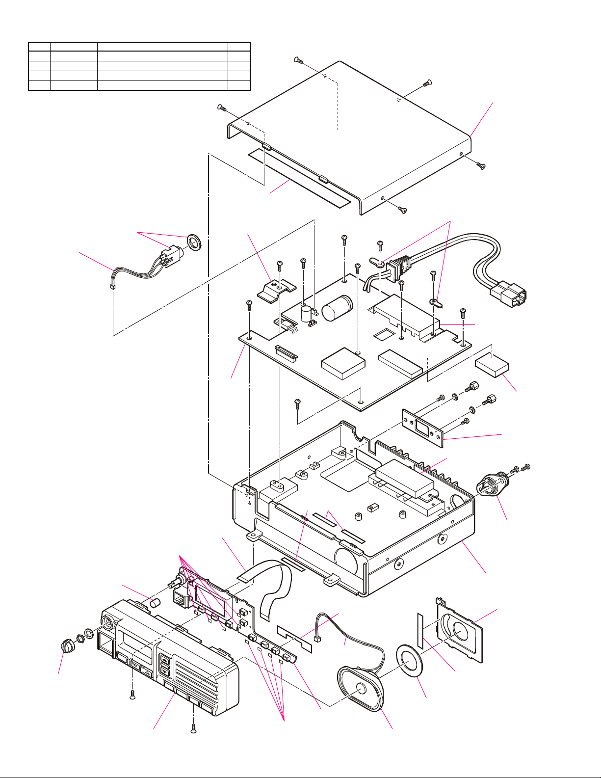
Exploded View & Miscellaneous Parts
REF.
VXSTD P/N
U20308002
•
U24306002
‚
U24308002
ƒ
U31206007
„
WIRE ASSY
T9206634A
BINDING HEAD SCREW M3 x 8 NI
DESCRIPTION
TAPTITE SCREW M3 x 6 NI
TAPTITE SCREW M3 x 8 NI
OVAL HEAD SCREW M2.6 x 6 B
CONNECTOR
P1090654
QTY.
2
10
2
7
„
BLIND SEET (130 x 10)
RA0424000
LEAF SPRING
RA0014700
‚
‚
„
‚
‚
‚
•
‚
„
„
CASE
RA0015100
„
TERMINAL STRIP
Q6000114
•
‚
SHIELD PLATE PA
R0124501
TUBE
RA0438500
BLIND SEET (4 x 2.5)
RA0405200
WIRE ASSY
BLIND SEET (4 x 3)
RA0405200
RF UNIT
RA0014700
‚
BLIND SEET (4 x 25)
RA0425500
BLIND SEET (34 x 8)
RA0404900
WIRE ASSY
T9206633
‚
‚
IC (POWER MODULE)
G1093631
CHASSIS
RA0152700
GAP PAD
S6000379
HOLDER
RA0014400
ƒ
ƒ
CONNECTOR
P1090984
SP HOLDER
RA0378300
VOLUME KNOB
RA0377000
4
4
„
PANEL ASSY
RA0376000
„
PANEL UNIT
BLIND SEET (4 x 3)
RA0405200
BLIND SEET (35 x 4)
RA0405000
SPONGE RUBBER
RA0383600
SPEAKER
M4090133
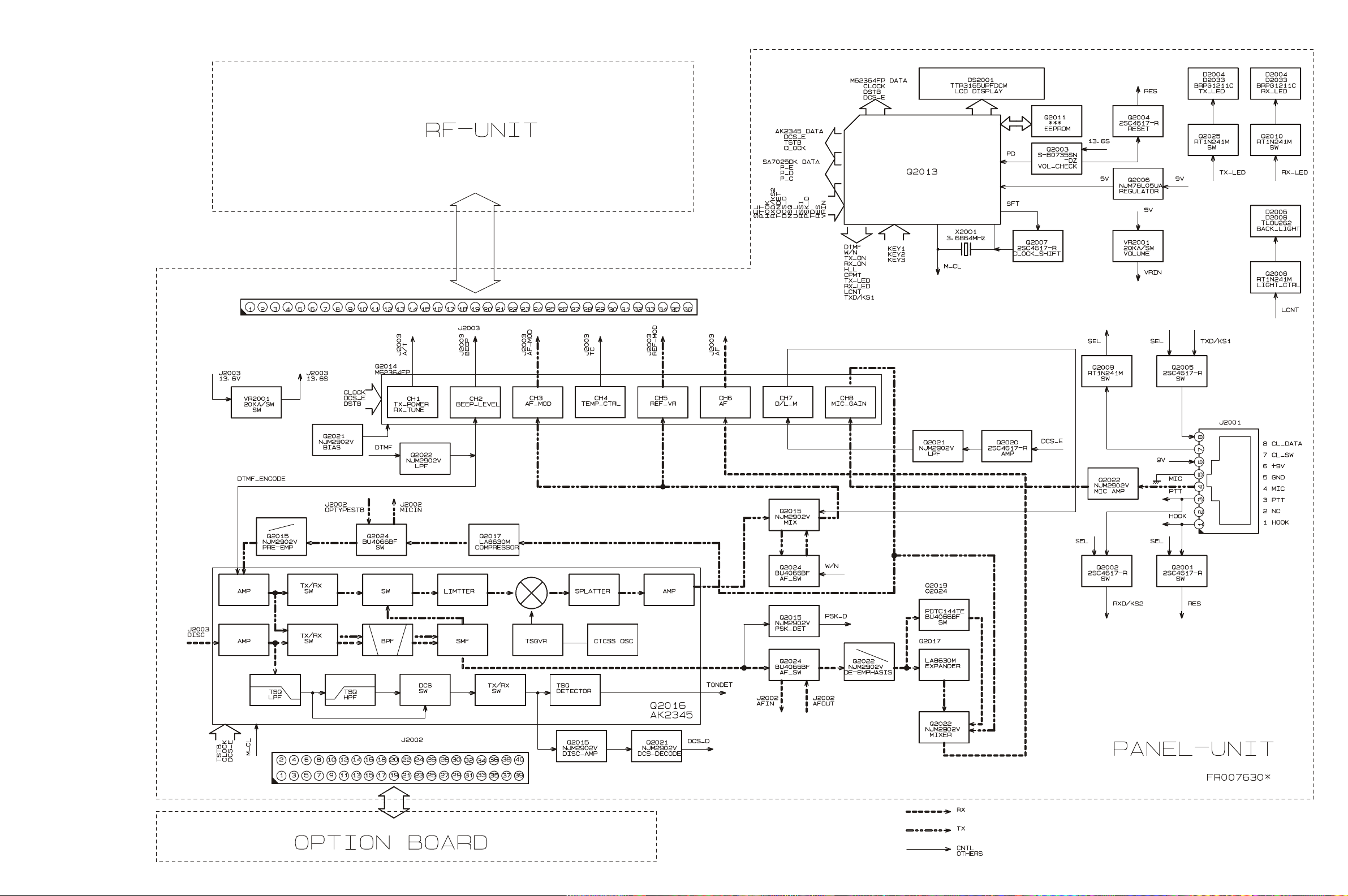
Block Diagram (1)
5
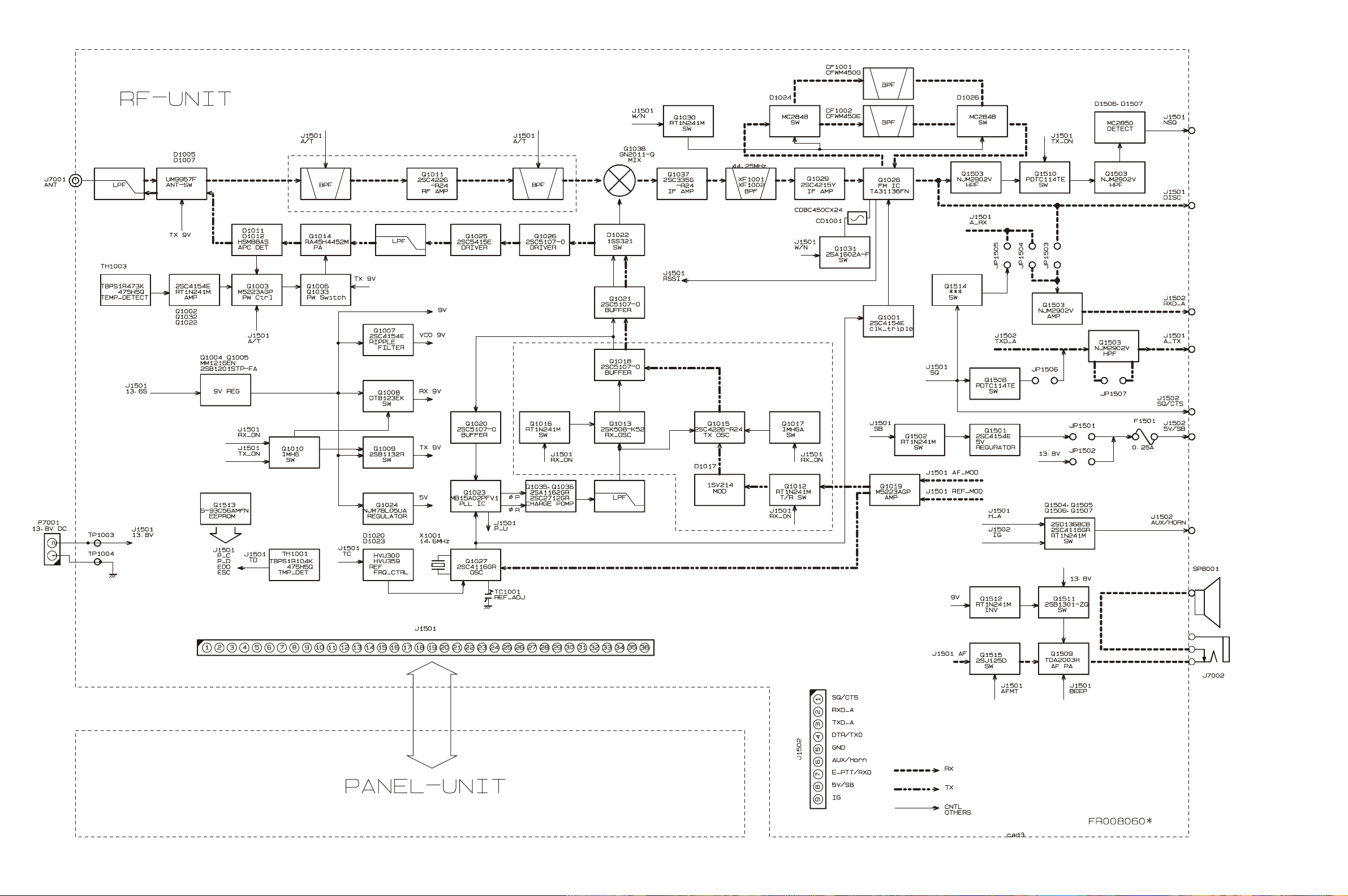
Block Diagram (2)
6
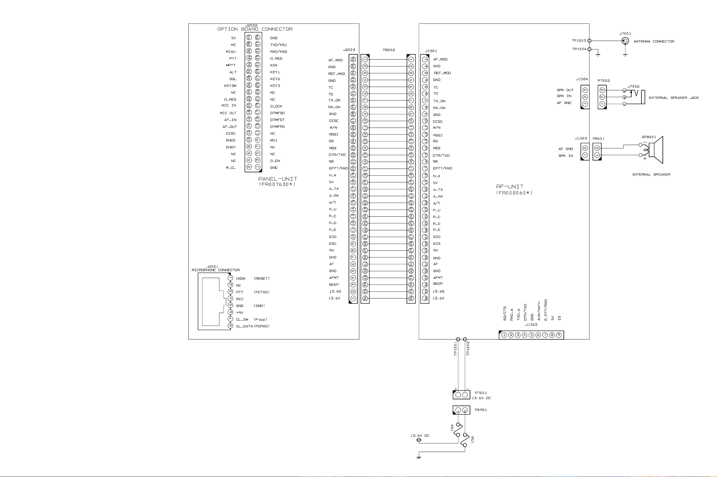
Interconnection Diagram
7

Note
8

Circuit Description
1. Overview
The VX-3200U is a UHF FM mobile transceiver designed
to operate in the frequency range of 400 to 512MHz.
2. Circuit Configuration by Frequency
The receiver is a double-conversion superheterodyne with
a first intermediate frequency (IF) of 44.25MHz and a second IF of 450kHz. Incoming signals from the antenna are
mixed with the local signal from PLL to produce the first
IF of 44.25MHz.
This is then mixed with the 43.8MHz second local oscillator (using the 14.6MHz reference crystal) output to produce the 450kHz second IF. This is detected to give the
demodulated signal.
The transmit signal frequency is generated by PLL VCO,
and modulated by the signal from the microphone. It is
then amplified and sent to the antenna.
3. Receive Signal Path
Incoming RF signals from the antenna connector are delivered to the RF Unit, and pass through a low-pass filter
(LPF) antenna switching network consisting of coils L1001,
L1002, L1003, L1004, and L1005, capacitors C1004, C1008,
C1009, C1011, and C1014, and antenna switching diodes
D1005 and D1007 (both UM9957F) for delivery to the re-
ceiver front end.
Signals within the frequency range of the transceiver are
then passed through a varactor-tuned bandpass filter consisting of L1008, L1009 before RF amplification by Q1011
(2SC4226).
The amplified RF is then band-pass filtered again by varactor-tuned resonators L1019, L1023 to ensure pure inband input to 1st mixer Q1038 (GN2011).
Buffered output from the VCO Unit is amplified by Q1021
(2SC5107) and low-pass filtered by L1030/L1031 and
C1184/C1188/C1192, to provide a pure 1st local signal
between 355.75 and 467.75MHz to the 1st mixer.
The 44.25MHz 1st mixer product then passes through dual
monolithic crystal filters XF1001 and XF1002, and is amplified by Q1029 (2SC4215Y) and delivered to the input
of the FM IF subsystem IC Q1028 (TA31136FN).
This IC contains the 2nd mixer, 2nd local oscillator, limiter amplifier, FM detector, noise amplifier, and squelch
gates.
The 2nd LO in the IF-IC is produced from crystal X1001
(14.600MHz), and the 1st IF is converted to 450kHz by the
2nd mixer and stripped of unwanted components by ceramic filter CF1001 or CF1002. After passing through a
limiter amplifier, the signal is demodulated by the FM
detector CD1001 (CDBC450CX24).
Detected audio from Q1028 (TA31136FN) is applied to
Q2016 (AK2345) and audio low-pass filter. After volume
adjustment by Q2014 (M62364FP), the audio signal is amplified by the AF power amplifier Q1509 (TDA2003H) and
passed to speaker jack.
4. Transmit Signal Path
Voice audio from the microphone is delivered via the MIC
(Jack) Unit to the PANEL Unit, after passing through
amplifier Q2022(NJM2902V), Mic gain-volume Q2014
(M62364FP) pre-emphasis Q2015 (NJM2902V), and limiter Q2016 (IDC instantaneous deviation control), is adjusted for optimum deviation level and delivered to the
next stage.
Voice input from the microphone and CTCSS are FMmodulated to the VCO of the synthesizer, while DCS audio is modulated by the reference frequency oscillator of
the synthesizer.
Synthesizer output, after passing through diode switch
D1022 (1SS321), is amplified by driver Q1025
(2SC5415E), Q1026 (2SC5107) and power module Q1039
(RA45H4452M) to obtain full RF output. The RF energy
then passes through antenna switch D1005/D1007 and a
low-pass filter circuit and finally to the antenna connector.
RF output power from the final amplifier is sampled by
CM coupler and is rectified by D1011, D1012 (both
HSM88AS). The resulting DC is fed through Automatic
Power Controller Q1003 (M5223AGP), Q1002
(RT1N241M), Q1032 (RT1N241M), Q1022 (RT1N241M),
and TH1003 to transmitter RF amplifier and thus the power output.
Generation of spurious products by the transmitter is minimized by the fundamental carrier frequency being equal
to the final transmitting frequency, modulated directly in
the transmit VCO. Additional harmonic suppression is
provided by a low-pass filter consisting of coils L1001,
L1003, L1004, capacitors C1004, C1008, C1009, C1011, and
C1014, resulting in more than 70dB of harmonic suppression prior to delivery to the RF energy to the antenna.
5. PLL Frequency Synthesizer
PLL frequency synthesizer consists of the VCO Q1013
(2SK508-K52: RX) and Q1015 (2SC4226-R24: TX), VCO
buffers Q1018, Q1020, Q1021 (all 2SC5107-0), PLL subsystem IC Q1023 (MB15A02PFV) and 14.6MHz reference
crystal X1001.
The frequency stability is ±2.5ppm within temperature
range of –30 to +60 degree. The output of the 14.6MHz
reference is applied to pin 8 of the PLL IC.
While receiving, VCO Q1013 oscillates between 355.75 and
467.75MHz according to the transceiver version and the
programmed receiving frequency. The VCO generates
355.75 to 467.75MHz for providing to the first local signal. In TX, the VCO generates 400 to 512MHz.
9

Circuit Description
The output of the VCO is amplified by the Q1020 and routed to the pin 5 of the PLL IC. Also the output of the VCO
is amplified by the Q1021 and routed first local/Power
Module according to D1022.
The PLL IC consists of a prescaler, fractional divider, reference divider and phase comparator and charge pump.
This PLL IC is fractional-N type synthesizer and performs
in the 40 or 50 kHz reference signal, which is eighth of the
channel step (5 or 6.25 kHz). The input signal from pin 5
and 8 of the PLL IC is divided down to the 20 kHz and
compared at phase comparator. The pulsed output signal
of the phase comparator is applied to the charge pump
and transformed into DC signal in the loop filter. The DC
signal is applied to the VCO and locked to keep the VCO
frequency constant.
PLL data is output from "DCS_E" (pin100), "CLOCK"
(pin2) and "PLL_E" (pin98) of the microprocessor Q2013.
The data are input to PLL IC when the channel is changed
or when transmission is changed to reception and vice
versa. A PLL lock condition is always monitored by the
pin20 of the Q2013. When the PLL is unlocked, the UL
goes low.
6. Miscellaneous Circuits
6-1 DCS Demodulator
DCS signals are demodulated on the PANEL-UNIT. It is
demodulated by Q2116 (AK2345), amplifier Q2015, and
comparator Q2021. This signal is provided to pin 25 of
Q2013 (MPU IC-LC87F72C8A) for its decording.
6-2 CTCSS encoder/decoder
The CTCSS code is generation and encoding by CTCSS
encoder/decoder IC Q2016 (AK2345).
7. Power Supply Circuits
7-1 All 13.6V
13.8V is always supplied to Power AMP Q1039
(RA45H4452M). Switched 13.6V is supplied to AF Power
AMP Q1509 (TDA2003H) and 9V Regulator Q1004
(MM1216EN) and Q1005 (2SB1201STP).
7-2 All 9V
9V regulated from 13.6V by Q1004 (MM1216EN) and
Q1005 (2SB1201STP).
7-3 VCO 9V
9V is filtered by Ripple Filter and is supplied to VCO Oscillator Q1013 (2SK508-K52), Q1015 (2SC5107-O), and
VCO BUFFER AMP Q1015 (2SC5107-O).
7-4 5V (RF-UNIT)
5V in RF-UNIT is regulated by REGULATOR IC Q1024
(NJM78L05UA). 5V is supplied to PLL IC Q1023
(MB15A02PFV), FM IC Q1028 (TA31136FN), and Reference Oscillator Q1027 (23C4116GR).
7-5 TX 9V
TX 9V is active on transmit. TX 9V is supplied to ANT SW
D1005, D1007 (UM9957F) and TX DRIVER Q1022
(2SC5415E), Q1025 (2SC5107-O).
7-6 RX 9V
RX 9V is active on receive. RX 9V is supplied to RX RF
AMP Q1026 (3SK228) and MIXER Q1011 (2SC4226-R34).
7-7 5V (RF-UNIT)
9V from RF-UNIT is regulated to 5V by REGULATOR IC
Q2006 (NJM78L05UA) in PANEL-UNIT.
6-3 MPU
Operation is controlled by 8-bit MPU IC Q2013. The system clock uses a 3.6864MHz crystal for a time base. IC
Q2003 (S-80735SN) resets the MPU when the power is
on, and monitors the voltage of the regulated 5V power
supply line.
6-4 DCS Encorder
The DCS code is generation and encoding by MPU IC
Q2013. It is filtered by Q2021 (NJM2902V) and adjusted
the level by Q2014 (M62364FP).
6-5 Compandor
The Compandor is active when pin90 of Q2013
(LC87F72C8A) is “High”. When the Compandor is active, MIC Audio is compressed, and detected audio is expanded by Q2017 (LA8630M).
6-6 2-Tone Decoder
A 2-Tone signal is demodulated on the PANEL-UNIT. It
is demodulated by Q2116 and comparator Q2021 . This
signal is provided to pin 26 of Q2013 (MPU IC-
LC87F72C8A) for its decording.
10

Alignment
Introduction
The VX-3200U is carefully aligned at the factory for the
specified performance across the frequency range specified for each version. Realignment should therefore not
be necessary except in the event of a component failure,
or altering version type. All component replacement and
service should be performed only by an authorized Vertex Standard representative,or the warranty policy may
be void.
The following procedures cover the sometimes critical and
tedious adjustments that are not normally required once
the transceiver has left the factory. However, if damage
occurs and some parts subsequently are placed, realignment may be required. If a sudden problem occurs during normal operation, it is likely due to component failure; realignment should not be done until after the faulty
component has been replaced.
We recommend that servicing be performed only by authorized Vertex Standard service technicians who are experienced with the circuitry and fully equipped for repair
and alignment. Therefore, if a fault is suspected, contact
the dealer from whom the transceiver was purchased for
instructions regarding repair. Authorized Vertex Standard
service technicians realign all circuits and make complete
performance checks to ensure compliance with factory
specifications after replacing any faulty components.
Those who do undertake any of the following alignments
are cautioned to proceed at their own risk. Problems
caused by unauthorized attempts at realignment are not
covered by the warranty policy. Also, Vertex Standard
reserves the right to change circuits and alignment procedures in the interest of improved performance, without
notifying owners.
Under no circumstances should any alignment be attempted unless the normal function and operation of the transceiver are clearly understood, the cause of the malfunction has been clearly pinpointed and any faulty components replaced, and realignment determined to be absolutely necessary.
The following test equipment (and thorough familiarity
with its correct use) is necessary for complete realignment.
Correction of problems caused by misalignment resulting from use of improper test equipment is not covered
under the warranty policy. While most steps do not require all of the equipment listed, the interactions of some
adjustments may require that more complex adjustments
be performed afterwards.
Required Test Equipment
r RF Signal Generator with calibrated output level
at 1000MHz
r Deviation Meter (linear detector)
r In-line Wattmeter with 5% accuracy at 1000MHz
r 50W RF Dummy Load with power rating 100W
at 1000MHz
r 4W AF Dummy Load
r Regulated DC Power Supply (standard 13.6V
DC, 15A)
r Frequency Counter with 0.1ppm accuracy at
1000MHz
r AC Voltmeter
r DC Voltmeter
r UHF Sampling Coupler
r IBM PC/compatible Computer
r Oscilloscope
r Vertex Standard VPL-1 Connection Cable &
Alignment program
Alignment Preparation & Precautions
A 50W RF Dummy Load and in-line wattmeter must be
connected to the main antenna jack in all procedures that
call for transmission, except where specified otherwise.
Correct alignment is not possible with an antenna.
After completing one step, read the following step to determine whether the same test equipment will be required.
If not, remove the test equipment (except dummy load
and wattmeter, in connected) before proceeding.
Correct alignment requires that the ambient temperature
be the same as that of the transceiver and test equipment,
and that this temperature be held constant between 68°F
and 86°F (20°C ~ 30°C). When the transceiver is brought
into the shop from hot or cold air, it should be allowed
time to come to room temperature before alignment.
Whenever possible, alignments should be made with oscillator shields and circuit boards firmly affixed in place.
Also, the test equipment must be thoroughly warmed up
before beginning.
Note: Signal levels in dB referred to in the alignment procedure are based on 0dBm EMF = 0.5mV.
Do not attempt to perform only a single step unless it is
clearly isolated electrically from all other steps. Have all
test equipment ready before beginning, and follow all of
the steps in a section in the order presented.
11
Alignment
Transceiver
Setup the test equipment as shown below, apply 13.6V
DC power to the transceiver.
The transceiver must be programmed for use in the intended system before alignment is attempted. The RF parameters are loaded from the file during the alignment
process.
Important
In order to facilitate alignment over the complete switching range of the equipment it is recommended that the
channel data in the transceiver is preset as the chart below.
CHANNEL
CH 1
CH 2
CH 3
CH 4
CHANNEL
SPACE
Wide
Narrow
Wide
Narrow
Version A
415.100 MHz
415.100 MHz
400.100 MHz
429.900 MHz
FREQUENCY (SIMPLEX
Version D
470.100 MHz
470.100 MHz
450.100 MHz
489.900 MHz
)
Version F
496.100 MHz
496.100 MHz
480.100 MHz
511.900 MHz
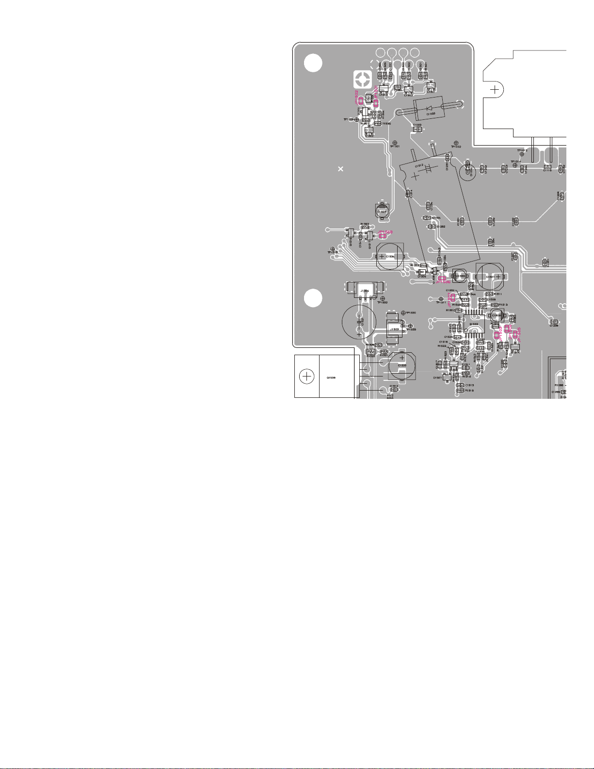
PLL VCV
Connect the positive lead of the DC voltmeter to
¦
the test point TP1007 (VCV) on the RF-Unit, as
indicated in the figure, and the negative lead to
chassis ground.
Set the transceiver to the high band edge fre-
¦
quency channel, then adjust coil L1016 on the
Unit for 7.45V on the voltmeter.
Key the transmitter, and adjust coil L1017 on the
¦
Unit for 7.25V on the voltmeter.
Next select to the low edge frequency channel
¦
and confirm above 2.00V to 3.00V on the voltmeter.
Key the transmitter, and confirm above 1.80V to
¦
2.50V on the voltmeter.
PLL Reference Frequency
With the wattmeter, dummy load and frequency counter
connected to the antenna jack, and select band center frequency channel, key the transmitter and adjust TC1001
on the RF-Unit, if necessary, so the counter frequency is
within 100 Hz of the channel center frequency for the transceiver version.
The alignment mode is accessed by “Alignment mode”
command from the computer whilst switching on. And it
is operated by the alignment tool automatically.
During the alignment mode, normal operation is suspended. Use the alignment tool program running on PC.
L1017
L1016
TC1001
TP1007
12
RF Unit Test & Alignment Points

Alignment
The alignment tool outline
Installation the tool
This alignment tool consists, MS-DOS based, only one execute file “svc52.exe.“ You make a directly as you think
fit, and copy this file. That is all of the installation process.
Boot the tool
Change directly and input in command line, “svc52 [enter],“ and boot the alignment tool.
Preparation
Setup the test equipment as “Alignment Preparation &
Precautions.”
Set the Ch. List to Table 1 on the CE52 Clone editor software.
Enter to the alignment mode
To enter the alignment mode, press “[0] Alignment Mode”
on the personal computer Key board. You turn off the
power of the transceiver, and turn on the transceiver. If
entry succeed,the alignment tool display as follows.
[0]Common TX
[1]Common RX
Action of the switches
When the transceiver is in alignment mode, the action of
[PTT], [MON], [UP], and [DOWN] is ignored. All of the
action is remote controlled by PC.
Menu of the tool
[0] Common TX
- [0] Tx Power High
This parameter is used to align TX High power (45 W).
Press [Enter] on “[0] Tx Power High” to align
¦
TX High power.
Select the Channel “1“ in alignment range.
¦
Press the [Space] key on the keyboard to acti-
¦
vate the transmitter.
Press the [UP] or [DWN] key, as needed, to set
¦
the power output to the following specification,
as indicated on the external wattmeter.
Tx Power High: 45 W (±1.0 W)
When the 45 Watt level is attained, press [Enter]
¦
to lock in the new data.
- [1] Tx Power Low
This parameter is used to align TX Low power (10 W).
Press [Enter] on “[1] Tx Power Low” to align TX
¦
Low power.
Select the Channel “1“ in alignment range.
¦
Press the [Space] key on the keyboard to acti-
¦
vate the transmitter.
Press the [UP] or [DWN] key, as needed, to set
¦
the power output to the following specification,
as indicated on the external wattmeter.
Tx Power Low: 10 W (±0.5 W)
When the 10 Watt level is attained, press [Enter]
¦
to lock in the new data.
- [2] VCO Deviation
This parameter is used to align the VCO Deviation.
Press [Enter] on “[2] VCO Deviation” to align
¦
VCO Deviation.
Select the Channel “1“ in alignment range.
¦
Adjust the AF generator output level to
¦
388mVrms (6dBm) at 1 kHz to the pin 3 of the
J1502 (D-sub 9pin ).
Press the [Space] key on the keyboard to acti-
¦
vate the transmitter.
Press the [UP] or [DWN] key, as needed, to set
¦
the VCO Deviation (Wide) to the following specification, as indicated on the deviation meter.
When the desired deviation level is attained,
¦
press [Enter] to lock in the new data.
Select the Channel 2, and set the VCO Deviation
¦
(Narrow), same as Channel “1.“
VCO Deviation (Wide): 4.0 kHz (±0.1 kHz)
VCO Deviation (Narrow): 2.0 kHz (±0.1 kHz)
13

Alignment
- [3] REF Deviation
This parameter is used to align the REF Deviation.
Press [Enter] on “[3] REF Deviation” to align REF
¦
Deviation.
Select the Channel “1“ in alignment range.
¦
Adjust the AF generator output level to
¦
388mVrms(–6dBm) at 100Hz to the pin 3 of the
J1502.
Press the [Space] key on the keyboard to acti-
¦
vate the transmitter.
Press the [UP] or [DWN] key, as needed, to set
¦
the modulation wave as follows.
Press [Enter] to lock in the new data.
¦
Select the Channel “2,“ and set the modulation
¦
wave, same as Channel “1.“
OK NG NG
- [4] CTCSS Deviation
This parameter is used to align the CTCSS deviation.
Press [Enter] on “[4] CTCSS Deviation” to align
¦
CTCSS Deviation.
Select the Channel “1“ in alignment range.
¦
Press the [Space] on the keyboard to activate the
¦
transmitter, and injects a CTCSS test tone.
Press the [UP]/[DWN] key, as need, to set the
¦
CTCSS Deviation (Wide) to the following specification.
Press [Enter] to lock in the new data.
¦
Select the Channel “2,“ and set the CTCSS De-
¦
viation (Narrow), same as Channel “1.“
CTCSS Deviation (Wide): 0.70 kHz (±0.1 kHz)
CTCSS Deviation (Narrow): 0.35 kHz (±0.1 kHz)
[1] Common RX
- [0] Tight NSQL
This parameter is used to align the noise level in squelch
Tight. It adjusts this alignment RX Tuning after ending.
Select the MID frequency channel in alignment
¦
range.
Set the SG output level to 0dBm EMF, and obey
¦
the message.
- [1] Threshold NSQL
This parameter is used to align the noise level in squelch
Threshold. It adjusts this alignment RX Tuning after ending.
Select the MID frequency channel in alignment
¦
range.
Set the SG output level to –7dBm EMF, and obey
¦
the message.
- [2] RX Tune
This parameter is used to align RX Tune.
Select the MID frequency channel in alignment
¦
range.
Set the SG output level to –6dBm EMF.
¦
Pressing the [DWN] key, reduce the RX Tune
¦
Level and set the SINAD above 12dB.
- [5] DCS Deviation
This parameter is used to align the DCS deviation.
Press [Enter] on “[5] DCS Deviation” to align
¦
DCS Deviation.
Select the Channel “1“ in alignment range.
¦
Press the [Space] key on the keyboard to acti-
¦
vate the transmitter, and injects a DCS test tone.
Press the [UP] or [DWN] key, as needed, to set
¦
the DCS deviation (Wide) to the following specification.
Press [Enter] to lock in the new data.
¦
Select the Channel “2,“ and set the DCS devia-
¦
tion (Narrow), same as Channel “1.“
DCS Deviation (Wide): 0.60 kHz (±0.1 kHz)
DCS Deviation (Narrow): 0.30 kHz (±0.1kHz)
The actual DCS deviation will increase around
¦
20% based on the above alignment as follows,
Actual DCS Deviation (Wide): 0.70 kHz
Actual DCS Deviation (Narrow): 0.35 kHz
14
JP1501 (JP1): Determine the output supply
voltage at pin 8 of DSUB 9-pin Accessory Connector.
Close: +5.0 V (Maximum 100 mA)
Open: No Action
JP1502 (JP2): Determine the output supply volt-
age at pin 8 of DSUB 9-pin Accessory Connector.
Close: +13.6 V (Maximum 100 mA)
Open: No Action
JP1503 (JP3): Determine the Rx discriminator
output characteristic at pin 2 of
DSUB 9-pin Accessory Connector.
Close: Flat 10 Hz to 3.0 kHz (140
mVrms / STD deviation with 600
ohm termination)
Open: No Action
JP1504 (JP4): Determine the Rx discriminator
output characteristic at pin 2 of
DSUB 9-pin Accessory Connector.
Close: Filtered 300 Hz to 3.0 kHz
(70 mVrms / STD deviation with
600 ohm termination)
Open: No Action
RF Unit Jumper Information
JP1505 (JP5): No Action (Spare Jumper).
JP1506 (JP6): Define whether the TX Data Input
at pin 3 of DSUB 9-pin Accessory
Connector shall be "on" or "off" according to the external PTT Input signal signal (pin 7 of DSUB
9-pin Accessory Connector).
Close: on (Enabled)
Open: off (Disabled)
JP1507 (JP7): Determine the TX Data Input level at pin 3 of DSUB 9-pin Accessory Connector.
Close: 400 mVrms / STD deviation with 600 ohm termination
Open: 40 mVrms / STD deviation with 600 ohm termination
JP1508 (JP8): Define whether the Transceiver's power shall be "on" or "off" according to the Ignition Signal
Input (pin 9 of DSUB 9-pin Accessory Connector).
Close: Turn the transceiver on when the Ignition Signal Input (pin 9 of DSUB 9-pin Accessory
Connector) is turned to "High" while the VOL/PWR knob is set to the "ON" position (out
of the click-stop position).
Open: No Action
15

Note
16
 Loading...