

UTMC 5962R-9865103VYX, 5962R-9865103VYC, 5962R-9865103QYX, 5962H-9865102VYX, 5962H-9865102VYC Datasheet
...
1
+FEATURES
q >400.0 Mbps (200 MHz) switching rates
q +340mV nominal differential signaling
q 3.3 V power supply
q TTL compatible inputs
q Cold sparing all pins
q Ultra low power CMOS technology
q 3.0ns maximum, propagation delay
q 0.4ns maximum, differential skew
q Radiation-hardened design; total dose irradiation testing to
MIL-STD-883 Method 1019
- Total-dose: 300 krad(Si) and 1Mrad(Si)
- Latchup immune (LET > 100 MeV-cm2/mg)
q Packaging options:
- 16-lead flatpack (dual in-line)
q Standard Microcircuit Drawing 5962-98651
- QML Q and V compliant part
INTRODUCTION
The UT54LVDS031LV Quad Driver is a quad CMOS
differential line driver designed for applications requiring ultra
low power dissipation and high data rates. The device is
designed to support data rates in excess of 400.0 Mbps (200
MHz) utilizing Low Voltage Differential Signaling (LVDS)
technology.
The UT54LVDS031LV accepts low voltage TTL input levels
and translates them to low voltage (340mV) differential output
signals. In addition, the driver supports a three-state function
that may be used to disable the output stage, disabling the load
current, and thus dropping the device to an ultra low idle power
state.
The UT54LVDS031LV and companion quad line receiver
UT54LVDS032LV provide new alternatives to high power
pseudo-ECL devices for high speed point-to-point interface
applications.
All pins have Cold Spare buffers. These buffers will be high
impedance when VDD is tied to VSS.
Standard Products
UT54LVDS031LV Low Voltage Quad Driver
Data Sheet
January 8, 2003
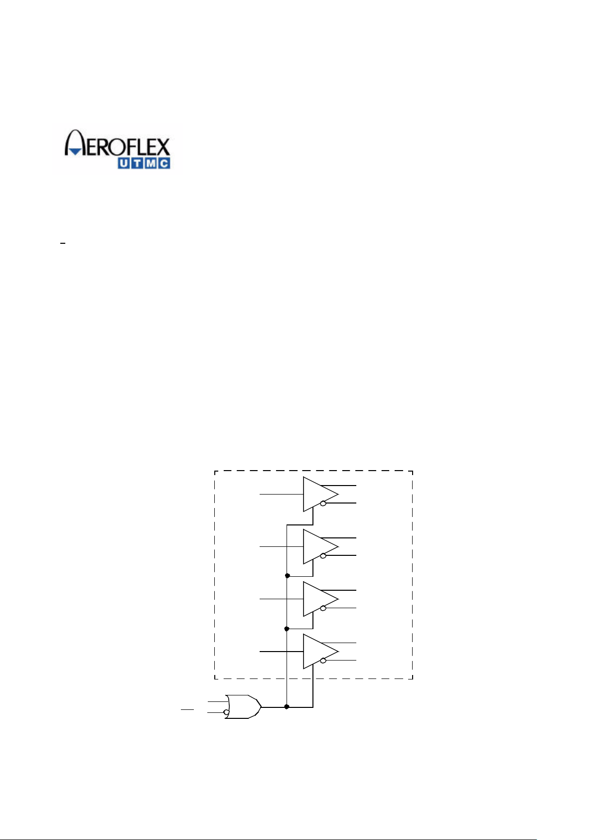
Figure 1. UT54LVDS031LV Quad Driver Block Diagram
D1
D2
D3
D4
D
OUT1+
D
OUT1-
D
OUT2+
D
OUT2-
D
OUT3+
D
OUT3-
D
OUT4+
D
OUT4-
D
IN1
D
IN2
D
IN4
D
IN3
EN
EN
2
TRUTH TABLE
PIN DESCRIPTION
APPLICATIONS INFORMATION
The UT54LVDS031LV driver’s intended use is primarily in an
uncomplicated point-to-point configuration as is shown in
Figure 3. This configuration provides a clean signaling
environment for quick edge rates of the drivers. The receiver is
connected to the driver through a balanced media such as a
standard twisted pair cable, a parallel pair cable, or simply PCB
traces. Typically, the characteristic impedance of the media is
in the range of 100Ω. A termination resistor of 100Ω should be
selected to match the media and is located as close to the receiver
input pins as possible. The termination resistor converts the
current sourced by the driver into voltages that are detected by
the receiver. Other configurations are possible such as a multireceiver configuration, but the effects of a mid-stream
connector(s), cable stub(s), and other impedance discontinuities,
as well as ground shifting, noise margin limits, and total
termination loading must be taken into account.
The UT54LVDS031LV differential line driver is a balanced
current source design. A current mode driver, has a high output
impedance and supplies a constant current for a range of loads
(a voltage mode driver on the other hand supplies a constant
voltage for a range of loads). Current is switched through the
load in one direction to produce a logic state and in the other
direction to produce the other logic state. The current mode
requires (as discussed above) that a resistive termination be
employed to terminate the signal and to complete the loop as
shown in Figure 3. AC or unterminated configurations are not
allowed. The 3.4mA loop current will develop a differential
voltage of 340mV across the 100 Ω termination resistor which
the receiver detects with a 240mV minimum differential noise
margin neglecting resistive line losses (driven signal minus
receiver threshold (340mV - 100mV = 240mV)). The signal is
centered around +1.2V (Driver Offset, VOS) with respect to
ground as shown in Figure 4. Note: The steady-state voltage
(VSS) peak-to-peak swing is twice the differential voltage (VOD)
and is typically 680mV.
Enables Input Output
EN EN D
IN
D
OUT+
D
OUT-
L H X Z Z
All other combinations
of ENABLE inputs
L L H
H H L
Pin No. Name Description
1, 7, 9, 15 D
IN
Driver input pin, TTL/CMOS
compatible
2, 6, 10, 14 D
OUT+
Non-inverting driver output pin,
LVDS levels
3, 5, 11, 13 D
OUT-
Inverting driver output pin,
LVDS levels
4 EN Active high enable pin, OR-ed
with EN
12 EN Active low enable pin, OR-ed
with EN
16 V
DD
Power supply pin, +3.3V + 0.3V
8 V
SS
Ground pin
Figure 2. UT54LVDS031LV Pinout
UT54LVDS031LV
Driver
16
15
14
13
12
11
10
9
V
DD
D
IN4
D
OUT4+
D
OUT4-
EN
D
OUT3-
D
OUT3+
D
IN3
1
D
IN1
2
D
OUT1+
3
D
OUT1-
4EN
5
D
OUT2-
6
D
OUT2+
7
D
IN2
8
V
SS
ENABLE
DATA
INPUT
1/4 UT54LVDS031LV
1/4 UT54LVDS032LV
+
-
DATA
OUTPUT
Figure 3. Point-to-Point Application
RT 100 Ω
3
The current mode driver provides substantial benefits over
voltage mode drivers, such as an RS-422 driver. Its quiescent
current remains relatively flat versus switching frequency.
Whereas the RS-422 voltage mode driver increases
exponentially in most cases between 20 MHz - 50 MHz. This
is due to the overlap current that flows between the rails of the
device when the internal gates switch. Whereas the current
mode driver switches a fixed current between its output without
any substantial overlap current. This is similar to some ECL
and PECL devices, but without the heavy static ICC
requirements of the ECL/PECL design. LVDS requires 80%
less current than similar PECL devices. AC specifications for
the driver are a tenfold improvement over other existing RS422 drivers.
The Three-State function allows the driver outputs to be
disabled, thus obtaining an even lower power state when the
transmission of data is not required.
D
IN
D
OUT-
D
OUT+
SINGLE-ENDED
D
OUT+
- D
OUT-
DIFFERENTIAL OUTPUT
V
0D
3V
0V
V
OH
V
OS
V
OL
+V
OD
-V
OD
0V
0V (DIFF.)
V
SS
Figure 4. Driver Output Levels
Note: The footprint of the UT54LVDS031LV is the same as the
industry standard Quad Differential (RS-422) Driver.
4
ABSOLUTE MAXIMUM RATINGS
1
(Referenced to VSS)
Notes:
1. Stresses outside the listed absolute maximum ratings may cause permanent damage to the device. This is a stress rating only, and functional operation of the device
at these or any other conditions beyond limits indicated in the operational sections of this specification is not recommended. E xposure to absolute maximum rating
conditions for extended periods may affect device reliability and performance.
2. Maximum junction temperature may be increased to +175°C during burn-in and life test.
3. Test per MIL-STD-883, Method 1012.
RECOMMENDED OPERATING CONDITIONS
SYMBOL PARAMETER LIMITS
V
DD
DC supply voltage -0.3 to 4.0V
V
I/O
Voltage on any pin during operation -0.3 to (VDD + 0.3V)
Voltage on any pin during cold spare -.3 to 4.0V
T
STG
Storage temperature -65 to +150 °C
P
D
Maximum power dissipation 1.25 W
T
J Maximum junction temperature
2
+150°C
Θ
JC
Thermal resistance, junction-to-case
3
10°C/W
I
I
DC input current
±10mA
SYMBOL PARAMETER LIMITS
V
DD
Positive supply voltage 3.0 to 3.6V
T
C
Case temperature range -55 to +125 °C
V
IN
DC input voltage 0V to V
DD
 Loading...