

UTMC 5962R-0153402VXX, 5962R-0153402VXC, 5962R-0153402VXA, 5962R-0153402QXX, 5962R-0153402QXC Datasheet
...
1
FEATURES
q 15 to 75 MHz shift clock support
q Low power consumption
q Power-down mode <216µW (max)
q Cold sparing all pins
q Narrow bus reduces cable size and cost
q Up to 1.575 Gbps throughput
q Up to 197 Megabytes/sec bandwidth
q 325 mV (typ) swing LVDS devices for low EMI
q PLL requires no external components
q Rising edge strobe
q Radiation-hardened design; total dose irradiation testing to
MIL-STD-883 Method 1019
- Total-dose: 300 krad(Si) and 1 Mrad(Si)
- Latchup immune (LET > 100 MeV-cm2/mg)
q Packaging options:
- 48-lead flatpack
q Standard Microcircuit Drawing 5962-01534
- QML Q and V compliant part
q Compatible with TIA/EIA-644 LVDS standard
INTRODUCTION
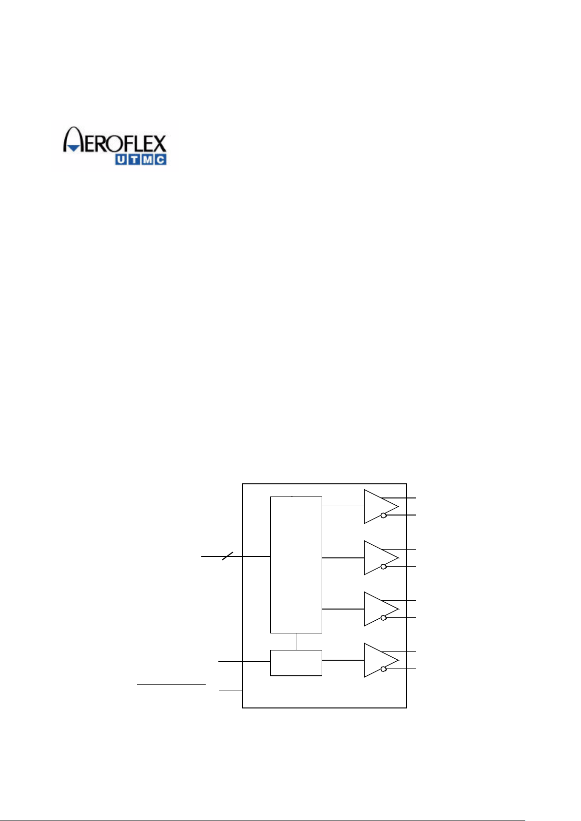
The UT54LVDS217 Serializer converts 21 bits of CMOS/TTL
data into three LVDS (Low Voltage Differential Signaling) data
streams. A phase-locked transmit clock is transmitted in parallel
with the data streams over a fourth LVDS link. Every cycle of
the transmit clock 21 bits of input data are sampled and
transmitted.
At a transmit clock frequency of 75MHz, 21 bits of TTL data
are transmitted at a rate of 525 Mbps per LVDS data channel.
Using a 75MHz clock, the data throughput is 1.575 Gbit/s (197
Mbytes/sec).
The UT54LVDS217 Serializer allows the use of wide, high
speed TTL interfaces while reducing overall EMI and cable size.
All pins have Cold Spare buffers. These buffers will be high
impedance when VDD is tied to VSS.
Standard Products
UT54LVDS217 Serializer
Data Sheet
June, 2003
TTL PARALLEL-TO-LVDS
PLL
POWER DOWN
TRANSMIT CLOCK IN
CMOS/TTL INPUTS
21
DATA (LVDS)
CLOCK (LVDS)
TTL PARALLEL -TO-
Figure 1. UT54LVDS217 Serializer Block Diagram
2
PIN DESCRIPTION
Figure 2. UT54LVDS217 Pinout
UT54LVDS217
48
47
46
45
44
43
42
41
N/C
LVDS GND
1TxIN4
2V
DD
3
4
5GND
6
7
8V
DD
9
10
11
12
13
14
15
16
TxIN6
TxIN5
TxIN7
TxIN8
TxIN9
TxIN10
GND
TxIN11
TxIN12
V
DD
TxIN13
TxIN14
17
18
19
20
21
22
23
24
TxIN15
TxIN17
TxIN16
V
DD
TxIN19
TxIN18
GND
GND
TxIN3
TxIN2
GND
TxIN1
TxIN0
TxOUT0-
40
39
38
37
36
35
34
33
TxOUT0+
TxOUT1-
LVDS GND
TxCLK OUT-
TxOUT1+
TxOUT2-
LVDS V
DD
TxOUT2+
32
31
30
29
28
27
26
25
PWR DWN
TxCLK IN
TxIN20
TxCLK OUT+
LVDS GND
PLL GND
PLL V
DD
PLL GND
Pin Name I/O No.
Description
TxIN I 21
TTL level input
TxOUT+ O 3
Positive LVDS differential data output
TxOUT- O 3
Negative LVDS differential data output
TxCLK IN I 1
TTL level clock input. The rising edge acts
as data strobe. Pin name TxCLK IN
TxCLK
OUT+
O 1
Positive LVDS differential clock output
TxCLK OUT- O 1
Negative LVDS differential clock output
PWR DWN I 1
TTL level input. Assertion (low input) TRISTATEs the clock and data outputs, ensuring low current at power down.
V
DD
I 4
Power supply pins for TTL inputs and logic
GND I 5
Ground pins for TTL inputs and logic
PLL V
DD
I 1
Power supply pins for PLL
PLL GND I 2
Ground pins for PPL
LVDS V
DD
I 1
Power supply pin for LVDS output
LVDS GND I 3
Ground pins for LVDS outputs
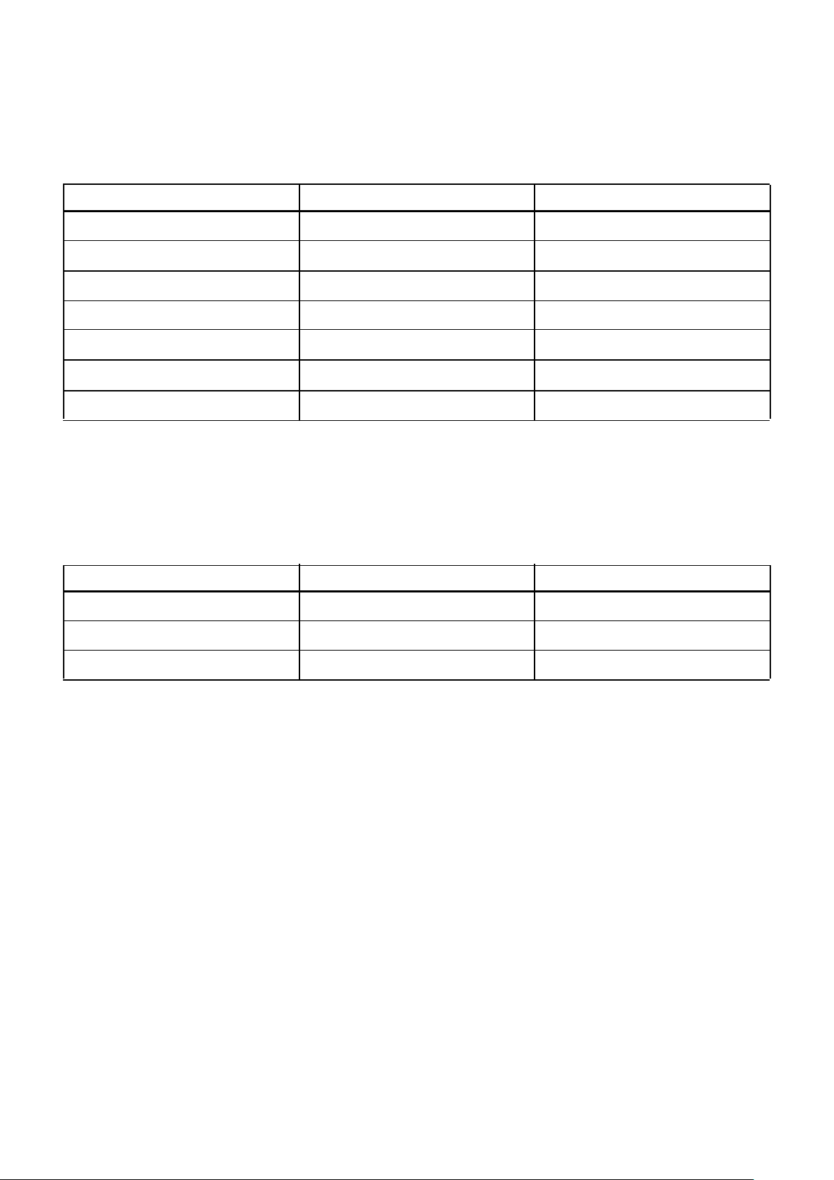
TxIN
UT54LVDS217
0
1
2
CMOS/
TTL
18
19
20
TxCLK
PCB
RxOUT
UT54LVDS218
0
1
2
18
19
20
RxCLK
PCB
SHIELD
GND
CLOCK
(LVDS)
DATA
(LVDS)
LVDS CABLE
MEDIA DEPENDENT
Figure 3. UT54LVDS217 Typical Application
3
ABSOLUTE MAXIMUM RATINGS
1
(Referenced to VSS)
Notes:
1. Stresses outside the listed absolute maximum ratings may cause permanent damage to the device. This is a stress rating only, and functional operation of the device
at these or any other conditions beyond limits indicated in the operational sections of this specification is not recommended. Exposure to absolute maximum rating
conditions for extended periods may affect device reliability and performance.
2. Maximum junction temperature may be increased to +175°C during burn-in and lifetest.
3. Test per MIL-STD-883, Method 1012.
4. For cold spare mode (VDD = VSS), V
I/O
may be 0.3V to the maximum recommended operating VDD + 0.3V.
RECOMMENDED OPERATING CONDITIONS
SYMBOL PARAMETER LIMITS
V
DD
DC supply voltage -0.3 to 4.0V
V
I/O Voltage on any pin
4
-0.3 to (VDD + 0.3V)
T
STG
Storage temperature -65 to +150°C
P
D
Maximum power dissipation 2 W
T
J Maximum junction temperature
2
+150°C
Θ
JC Thermal resistance, junction-to-case
3
10°C/W
I
I
DC input current
±10mA
SYMBOL PARAMETER LIMITS
V
DD, PLLVDD,
LVDS V
DD
Positive supply voltage 3.0 to 3.6V
T
C
Case temperature range -55 to +125°C
V
IN
DC input voltage 0V to V
DD
4
DC ELECTRICAL CHARACTERISTICS
1
(VDD = 3.3V-0.3V; -55°C < TC < +125°C)
Notes:
1. Current into device pins is defined as positive. Current out of device pins is defined as negative. All voltages are referenc ed to ground.
2. Output short circuit current (IOS) is specified as magnitude only, minus sign indicates direction only. Only one output should be shorted at a time, do not exceed
maximum junction temperature specification.
3. Guaranteed by characterization.
4. Devices are tested @ 3.6V only.
5. Clock outputs guaranteed by design.
6. Post 100Krad and 300Krad, I
CCZ
= 200µA.
SYMBOL PARAMETER CONDITION MIN MAX UNIT
CMOS/TTL DC SPECIFICATIONS
V
IH
High-level input voltage 2.0 V
DD
V
V
IL
Low-level input voltage GND 0.8 V
I
IH
High-level input current VIN = 3.6V; VDD = 3.6V -10 +10 µA
I
IL
Low-level input current
VIN = 0V; VDD = 3.6V
-10 +10 µA
V
CL
Input clamp voltage ICL = -18mA -1.5 V
I
CS
Cold Spare Leakage current VIN = 3.6V; VDD = V
SS
-20 +20 µA
LVDS OUTPUT DC SPECIFICATIONS (OUT+, OUT-)
V
OD
5
Differential Output Voltage RL = 100Ω (See Figure 14)
250
400 mV
∆V
OD
5
Change in VOD between
complimentary output states
RL = 100Ω (See Figure 14) 35 mV
V
OS
5
Offset Voltage
RL = 100Ω,
1.120
1.410 V
∆V
OS
5
Change in VOS between
complimentary output states
RL = 100Ω 35 mV
I
OZ
4
Output Three-State Current PWR DWN = 0V
V
OUT
= 0V or V
DD
-10 +10 µΑ
I
CSOUT
Cold Spare Leakage Current VIN=3.6V, VDD = V
SS
-20 +20 µΑ
I
OS
2,3
Output Short Circuit Current
V
OUT
+ or V
OUT
-
= 0V
5mA mA
Supply Current
I
CCL
4
Transmitter supply current with
loads
RL = 100Ω all channels
(figure 4)
CL = 5pF, f = 50MHz
65.0 mA
I
CCZ
4,6
Power down current DIN = V
SS
PWR DWN = 0V, f = 0Hz
60.0 µA
Vos
Voh Vol
+
2
---------------------------
=
 Loading...