

UTMC 5962R0150202VYC, 5962R0150202VXC, 5962R0150202QYC, 5962R0150202QXC, 5962R0150201VYC Datasheet
...
Standard Products
UT1750AR RadHard RISC Microprocessor
Data Sheet
May 2003
FEATURES
q Operates in either RISC (Reduced Instruction Set
Computer) mode or MIL-STD-1750A mode
q Supports MIL-STD-1750A 32-bit floating-point
operations and 48-bit extended-precision floating-point
operations on chip
q Built-in 9600 baud UART
q Supports defined MIL-STD-1750A Console Mode of Operation
q Full 64K-word address space. Expandable to 1M words with
optional MMU (operand port)
q Register-oriented architecture has 21 user-accessible registers
q Registers may be in 16-bit word or 32-bit double-word
configurations
q Built-in multiprocessor bus arbitration and Direct Memory Access
support (DMA)
q TTL-compatible I/O
q Stable 1.5-micron CMOS technology
q Full military operating range, -55°C to +125°C, in accordance
with MIL-PRF-38535 for Class Q and V
q Typical radiation performance
- Total dose: 1.0E6 rads(Si)
- SEL Immune . 100 MeV-cm2/mg
- LETTH(0.25) = 60 MeV-cm2/mg
- Saturated Cross Section (cm2) per bit, 1.2E-7
- 2.3E-11 errors/bit-day, Adams to 90% geosynchronous heavy ion
q Standard Military Drawing 5962-01502
PROCES-
SOR
STATUS
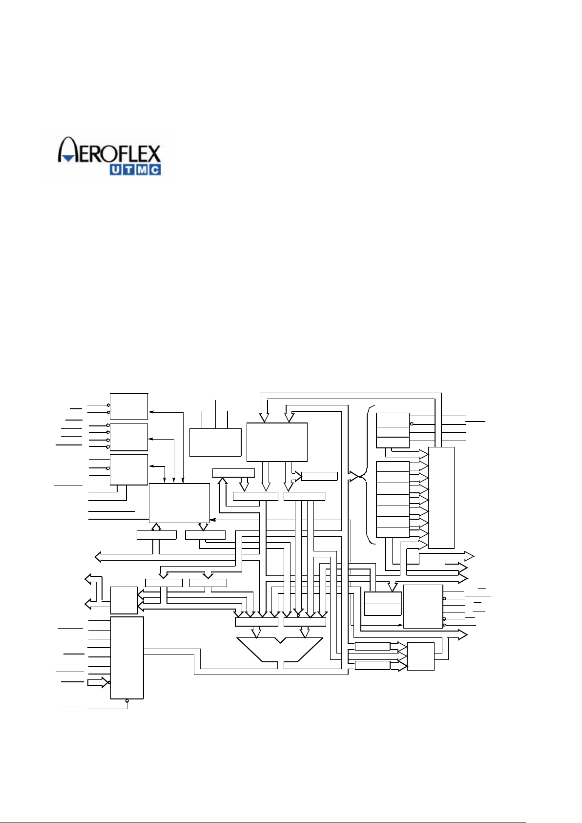
Figure 1. UT1750AR Functional Block Diagram
OE
WE
BRQ
BGNT
BUSY
BGACK
NUI1
NUI2
M1750
STATE1
MME
CONSOLE
RISC DATA
RISC
ADDRESS
SYSFL
BTERR
MPAR
MPROT
PFAIL
IOLINT1
IOLINT0
INT0-5
MRST
16
RISC
ADD
MUX
RISC
MEMORY
CONTROL
BUS
ARBITRA-
TION
PROCESSOR
CONTROL
LOGIC
OSCILLATOR
/CLOCK
GENERAL
PURPOSE
REGISTERS
OSCIN
OSCOUT
SYSCLK
IR
IC/ICs ACC
SHIFT REG
TEMP DEST16TEMP SRC
BIT REG
A MUX B MUX
32-BIT ALU
16
16
ADDR
MUX
BUS
CONTROL
UART
TBR
RBR
TIMCLK
TEST
UARTOUT
UARTIN
TR
TB
IM
FR
PI
ST
SW
16
8
AS0-3
OPERAND
DATA
DTACK
M/IO
R/WR
DS
OPERAND
ADDRESS
I/O
MUX
16
6
32
32
32
323232
32
32
NUO3
PIPELINE
PR
OP/IN
AS
1750 PC
32
1750 SP
RISC MAP
4
4
PS0-3
16
16
16
16
16
16
16
I
N
T
E
R
R
U
P
T
S
16
RISC
ADDRESS
2
DS
AS
R/WR
M/IO
DTACK
OP/IN
BGACK
BUSY
BGNT
BRQ
SYSFLT
WE
OE
MRST
IOLINT1
IOLINT0
PFAIL
INT0
INT1
INT2
INT3
INT4
INT5
TEST
EXCEPTIONS
INTERRUPTS/
RISC DATA PORT
OSCIN
OSCOUT
UARTIN
UARTOUT
TIMCLK
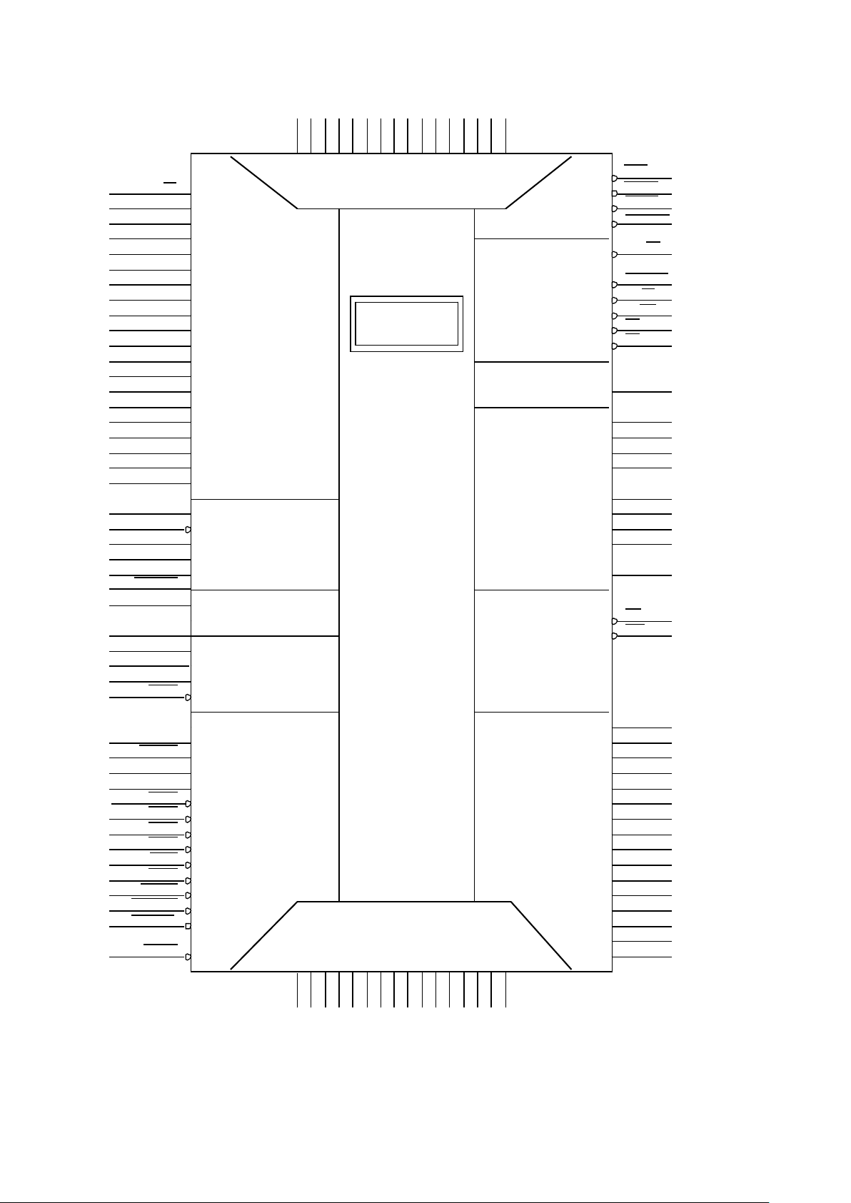
UT1750AR
RA19/CS
RA18/OD1
RA17/OD2
RA16/OD3
RA15
RA14
RA13
RA12
RA11
RA10
RA9
RA8
RA7
RA6
RA5
RA4
RA3
RA2
RA1
RA0
NUI1
M1750
BTERR
MPAR
MPROT
A0
A1
A2
A3
A4
A5
A6
A7
A8
A9
A10
A11
A12
A13
A14
A15
NUO3
PS3
PS2
PS1
PS0
AS3
AS2
AS1
SYSCLK
RISC
ADDRESS
BUS
PROCESSOR
STATUS
OSCILLATOR
UART
DATA BUS
MEMORY
ADDRESS
BUS
CLOCK
MODE
BUS
CONTROL
BUS
ARBITRATION
AS0
Figure 2. UT1750AR Pin Function Diagram
MME
CONSOLE
STATE1
RD0 - RD15
D0 - D15
OPERAND
OPERAND
NUI2
3
GENERAL DESCRIPTION
The UT1750AR (figures 1 and 2) is a high performance
monolithic CMOS 16-bit RISC microprocessor that supports
the complete MIL-STD-1750A Instruction Set Architecture
(ISA). Underlying the MIL-STD-1750A support is a highperformance RISC that provides MIL-STD-1750A emulation
capability. Developed to provide effective real-time avionics
processing, the high performance of the native RISC machine
is available to the MIL-STD-1750A systems designer through
the MIL-STD-1750A Built-In-Function (BIF) opcode.
The UT1750AR is the first member of a family of highperformance MIL-STD-1750 processors and support
peripherals from UTMC.
PRODUCT DESCRIPTION
The UTMC UT1750AR operates in its native RISC language
mode or MIL-STD-1750A ISA mode. As a MIL-STD-1750A
microprocessor, the UT1750AR requires 8K x 16 of ROM to
map the MIL-STD-1750A instruction set into the native RISC
machine language instructions. Each MIL-STD-1750A opcode
has a unique RISC code macro in the external ROM. The
UT1750AR executes the corresponding resident RISC code
macro to perform the MIL-STD-1750A instruction
requirements. When in this mode and operating with a 12 MHz
clock, the UT1750AR can throughput 600 KIPS using the DAIS
mix (800 KIPS @ 16 MHz).
The native RISC language mode is available to the user when
the UT1750AR is operating as MIL-STD-1750A processor
through MIL- STD-1750A’s Built-In Function (BIF) opcode.
When operating as a RISC processor, the UT1750AR executes
most RISC instructions in two clock cycles. Thus, a 12 MHz
operating clock frequency provides up to 6 MIPS of RISC
throughput (8 MIPS @16 MHz). This high execution rate, along
with its efficient architecture, make the RISC mode especially
effective in applications requiring real-time processing.
The architecture of the UT1750AR is based around 20 useraccessible, 16-bit general purpose registers providing the
programmer with extensive register support. The UT1750AR’s
flexibility is enhanced by its ability to concatenate the 16-bit
registers into ten 32-bit registers. In addition, all registers are
available for use as either the source or the destination for any
register operation.
The UT1750AR fully supports multiprocessor, DMA, and
complex bus arbitration for managing the system bus and
preventing bus contention. Bus control passes among bus
masters operating on the same bus. The bus masters can be
several UT1750ARs or any other device requiring Direct
Memory Access, such as a MIL-STD-1553B interface.
The UT1750AR supports 16 levels of vectored interrupts. Ten
of these are external interrupts, eight of which are userdefinable. All 16 interrupt levels are prioritized and serviced in
order of priority.
When used as a MIL-STD-1750A microprocessor, the
UT1750AR’s instruction set supports 16-bit fixed-point singleprecision and 32-bit fixed-point double-precision data formats.
Also, the UT1750AR can emulate 32-bit floating-point and 48bit floating-point extended-precision data in two’s complement
representation.
In its native RISC mode, the UT1750AR’s three basic
instruction formats support 16-bit and 32-bit instructions. The
formats are Register-to-Register, Register-to-Literal, and
Register-to-Long-Immediate instructions.
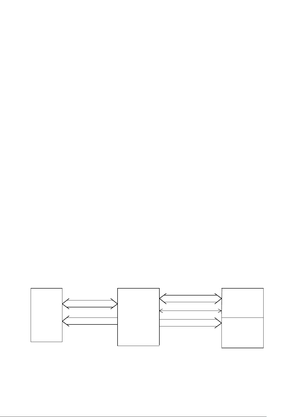
Figure 3 shows the UT1750AR’s general system architecture,
its emulation ROM, instruction and data memory, and the
system interface. The emulation ROM is isolated from the
system; only the UT1750AR microprocessor accesses it.
MEMORY
MIL-STD-1750A
16
16
16
16
ADDRESSOPERAND
Figure 3. UT1750AR MIL-STD-1750A General System Architecture
CONTROL
DATAOPERAND
(8K X 16)
ROM
EMULATION
RISC ADDRESS
RISC DATA
UT1750AR
INSTRUCTIONS
DATA
4
FUNCTIONAL PINOUT
Legend for TYPE and ACTIVE fields:
TO = TTL output
TI = TTL input
TUI = TTL input (pull-up)
TDI = TTL input (pull-down)
TTO = Three-state TTL output
TTB = Three-state TTL bidirectional
CO = CMOS output
OSC = Oscillator input to a Pierce Oscillator inverter
AH = Active High
AL = Active Low
OSCIN 50 P14 OSC
OSCILLATOR AND CLOCK SIGNALS
PIN NAME
PIN NUMBER
FLTPK PGA
TYPE ACTIVE DESCRIPTION
OSCOUT
SYSCLK
51
52
P15
M14
CO
TO
Oscillator Input. A 50% duty cycle crystal-drive input for
driving the UT1750AR.
Oscillator Output. A 50% duty cycle, single-phase clock
output at the same frequency as the OSCIN input.
System Output. The buffered equivalent of the OSCOUT
signal.
NUI1 129 H2 TI
PROCESSOR STATUS
PIN NAME
PIN NUMBER
FLTPK PGA
TYPE ACTIVE DESCRIPTION
NUI2
NUO3
44
126
P12
G3
TUI
TTO
Not used input 1. Internal UTMC use only. Tie either high
or low.
Not used input 2. Internal UTMC use only. Tie low.
Not used output 3. Internal UTMC use only. NUO3 enter
high impedance state when the UT1750AR is in the test
mode (TEST=0)
--
--
--
M1750 45 N11 TDI
AH
STATE1
Mode Select RISC/1750. A high on M1750 places the
UT1750AR into the MIL-STD-1750A emulation mode.
A low on M1750 places the UT1750AR into the RISC
mode. It is tied to an internal pull-down resistor.
54 N15 TTO
Processor State. This signal indicates the internal state of
the UT1750AR. A low on STATE1 indicates the
UT1750AR is executing a new RISC instruction. A high
on STATE1 indicates the UT1750AR is fetching a RISC
instruction. STATE1 enters a high-impedance state when
the UT1750AR is in the test mode (TEST=0).
--
--
--
--
5
Operand/Instruction. This indicates whether the
UT1750AR’s current bus cycle is for Data (high) or
Instruction (low) acquisition. OP/IN remains in a high
state whenever a bus cycle (Memory or I/O) is not an
instruction fetch.
BRQ 118 D2 TTO
OPERAND DATA BUS ARBITRATION
PIN NAME
PIN NUMBER
FLTPK PGA
TYPE ACTIVE DESCRIPTION
BGNT
BUSY
119
120
E3
C1
TUI
TUI
Bus Request. The UT1750AR asserts this signal to indicate
it is requesting control of the Operand data bus (D0 - D15).
BRQ enters a high-impedance state when the UT1750AR is
in the test mode (TEST = 0).
Bus Grant. When asserted, this signal indicates the
UT1750AR may take control of the Operand data bus. It is
tied to an internal pull-up resistor.
Bus Busy. A bus master asserts this input to inform the
UT1750AR that another bus master is using the Operand
data bus. It is tied to an internal pull-up resistor.
OP/IN 113 A2 TTO
OPERAND DATA BUS CONTROL
PIN NAME
PIN NUMBER
FLTPK PGA
TYPE ACTIVE DESCRIPTION
DTACK
M/IO
121
112
E2
B3
TUI
TTO
Data Transfer Acknowledge. This signal tells the
UT1750AR that a data transfer has been acknowledged
and the UT1750AR can complete the bus cycle. To assure
the UT1750AR operates with no wait states, DTACK can
be tied low. DTACK is tied to an internal pull-up resistor.
Memory or I/O. Indicates whether the current bus cycle
is for memory (high) or I/O (low). It remains in the highimpedance state during bus cycles when the UT1750AR
does not control the Operand busses.
AL
BGACK 117 B1 TTO
AL
AL
AL
AL
Bus Grant Acknowledge Output. The UT1750AR asserts
this signal to indicate it is the current bus master. When low,
BGACK inhibits other devices from becoming the bus
master. When the UT1750AR relinquishes control of the
bus, BGACK enters a high-impedance state.
R/WR 114 C4 TTO
Read/Write. Indicates the direction of data flow with
respect to the UT1750AR. R/WR high means the
UT1750AR is attempting to read data from an external
device, and R/WR low means the UT1750AR is
attempting to write data to an external device. R/WR
remains in a high-impedance state when the UT1750AR
does not control the Operand busses.
Continued on page 6.
--
--
--
6
Output Enable RISC Memory. This signal
allows RISC memory to place data on the RISC instruction
data bus. The Store Register to Instruction Memory (STRI)
instruction removes OE during the CK2 internal clock
cycle. OE enters a high-impedance state when the
UT1750AR is in the test mode (TEST = 0).
AS 115 C3 TTO
OPERAND DATA BUS CONTROL
PIN NAME
PIN NUMBER
FLTPK PGA
TYPE ACTIVE DESCRIPTION
DS 116 B2 TTO
Address Strobe. Indicates a valid address on the Operand
Address bus. UT1750AR places AS in a high-impedance
state when it does not control the Operand busses.
Data Strobe. Indicates valid data is on the Operand Data bus.
The UT1750AR places DS in a high-impedance state when
it does not control the Operand busses.
OE 42 R12 TTO
RISC MEMORY CONTROL
PIN NAME
PIN NUMBER
FLTPK PGA
TYPE ACTIVE DESCRIPTION
WE 43 R13 TTO
Write Enable RISC Memory. This signal allows the
UT1750AR to write to RISC instruction memory. The
Store Register to Instruction Memory (STRI) instruction
asserts WE during the CK2 internal clock cycle. WE
enters a high-impedance state when the UT1750AR is in
the test mode (TEST = 0).
AL
AL
AL
Continued from page 5.
AL
UART CONTROL/TIMER CLOCK
UARTIN 127 F1 TUI
PIN NAME
PIN NUMBER
FLTPK PGA
TYPE ACTIVE DESCRIPTION
UARTOUT 128 G1 TTO
AH
AH
UART Input. The UT1750AR receives serial data
through this input. The serial data is stored in the
UT1750AR’s Receiver Buffer Register (RCVR). It is tied
to an internal pull-up resistor.
UART Output. The serial data stored in the UT1750AR’s
Transmitter Buffer Register (TXMT) is transmitted
through this output. The UART output is fixed at 9600
baud, with eight data bits, odd-parity, and one stop bit.
UARTOUT enters a high-impedance state when the
UT1750AR is in the test mode (TEST=0). (9600 baud @
TIMCLK = 12MHz)
Continued on page 7.
7
Test (Input). Asserting this input places the UT1750AR
into a test mode. In this mode, all the UT1750AR’s
outputs, except OSCOUT and SYSCLK, enter a highimpedance state. When using TEST, the UT1750AR
must have a MRST. MRST must be held active for at
least one SYSCLK period after TEST is
deasserted to assure proper operation (see figure 42b).
TEST is tied to an internal pull-up resistor.
TIMCLK 53 L13 TI
UART CONTROL/TIMER CLOCK
PIN NAME
PIN NUMBER
FLTPK PGA
TYPE ACTIVE DESCRIPTION
CONSOLE 48 N12 TDI
Timer Clock. This 12 MHz clock input generates the baud
rate for the UT1750AR’s internal UART. The input also
provides the clock for the UT1750AR’s two internal MILSTD-1750A timers (TIMER A and TIMER B).
Console (Command). Asserting this input sets bit 3 in the
System Status Register. Bit 3 is read with the Input Register
Instruction (INR). When the UT1750AR is operating in the
MIL-STD-1750 mode, asserting CONSOLE during a
Master Reset invokes the maintenance console option. Tied
to an internal pull-down resistor.
TEST 46 P13 TUI
MME 49 N13 TDI
AH
Memory Management Enable. This signal indicates to
the UT1750AR that a Memory Management Unit
(MMU) is present and that the memory management
option is enabled. MME is tied to an internal pull-down
resistor.
AH
AL
PROCESSOR MODE
AS0 104 B7 TTO
PIN NAME
PIN NUMBER
FLTPK PGA
TYPE ACTIVE DESCRIPTION
PS0 108 A4 TTO
AH
AH
Address State. These outputs indicate the current address
state of the UT1750AR. Using these outputs with a
Memory Management Unit (MMU) allows selecting the
MMU’s page register group. These outputs enter a
high-impedance state when the UT1750AR is placed in
the test mode (TEST=0) or during bus cycles not assigned
to this processor.
Processor State. These outputs indicate the current state
of the processor. These outputs enter a high-impedance
state when the UT1750AR is in the test mode (TEST=0)
or during bus cycles not assigned to this processor.
AS1
AS2
AS3
105
106
107
B6
C6
A5
PS1
PS2
PS3
109
110
111
A3
B4
C5
--
Continued from page 6
8
Memory Parity (Error). Asserting this input indicates a MIL-STD1750 memory parity error. Bit 13 of the UT1750AR’s Fault
Register, Memory Parity Fault, is set when MPAR is active. Under
no circumstances should MPAR be tied in its active state. It is tied
to an internal pull-down resistor. Interrupt is not cleared via
software until the negation of the input signal.
SYSFLT 125 G2 TUI
INTERRUPTS/EXCEPTIONS
PIN NAME
PIN NUMBER
FLTPK PGA
TYPE ACTIVE DESCRIPTION
BTERR 122 D1 TUI
System Fault. This positive edge-triggered input sets bit 8
(SYSFLT) in the UT1750AR’s Fault Register. Under no
circumstances should SYSFLT be tied in its active state. It
is tied to an internal pull-up resistor.
MPAR
Bus Time Error. It is asserted when a bus error or a timeout occurs.
During I/O bus cycles, an active BTERR sets bit 10 of the Fault
Register. During Memory bus cycles, an active BTERR sets bit 7
of the Fault Register. Under no circumstances should BTERR be
tied in its active state. It is tied to an internal pull-up resistor.
Interrupt is not cleared via software until the negation of the input
signal.
124 F2 TDI
MPROT 123 F3 TUI
AH
Memory Protect Fault. When asserted, it informs the UT1750AR that
a memory-protect fault has occurred on the Operand Data Bus. An
access fault, a write-protect fault, or an execute-protect fault causes a
memory-protect fault. If the UT1750AR is using the bus and MPROT
is asserted, bit 15 of the Fault Register (CPU Fault) is set. If the
UT1750AR is not using the bus and MPROT is asserted, bit 14 of the
Fault Register (DMA Error) is set. It is tied to an internal pull-up
resistor. Interrupt is not cleared via software until the negation of the
input signal.
AL
AH
INT0 56 M15 TUI
IOLINT0 62 J15 TUI
User Interrupts. These interrupts are active on a negativegoing edge and each will set, when active, its associated bit
in the Pending Interrupt Register. The interrupts are maskable
by setting the associated bits in the Interrupt Mask Register.
Asserting MRST resets all interrupts. They are tied to an
internal pull-up resistor.
I/O Level Interrupts. These inputs are active on a negativegoing edge and each sets, when active, its associated bit in
the Pending Interrupt Register. The interrupts are maskable
by setting the associated bits in the Interrupt Mask Register.
Asserting MRST resets all interrupts. They are tied to an
internal pull-up resistor.
INT1
INT2
INT3
INT4
INT5
57
58
59
60
61
K13
K14
J14
J13
K15
IOLINT1 63 H14
PFAIL 55 L14 TUI AL Power Fail (Interrupt). Asserting this input informs the
UT1750AR that a power failure has occurred and the present
process will be interrupted. This input sets bit 15 in the Pending
Interrupt Register. A Power Fail Interrupt (bit 15) cannot be
disabled. When operating in the RISC mode, the UT1750AR
must be reset after a PFAIL to assure normal operation. It is
tied to an internal pull-up resistor.
MRST 47 R14 TUI AL
Master Reset. This input initializes the UT1750AR to a
reset state. The UT1750AR must be reset after power
(Vcc) is within specification and stable to ensure proper
operation. The system must hold MRST active for at least
one period of SYSCLK to assure the UT1750AR will be
reset. It is tied to an internal pull-up resistor.
AH
AL
AL
9
A0 84 A14 TTO
OPERAND BUSSES
PIN NAME
PIN NUMBER
FLTPK PGA
TYPE ACTIVE DESCRIPTION
Address Bus - Operand. When asserted, this bus is
unidirectional and represents the Operand Address. The bus
is in the high-impedance state when the UT1750AR does
not control the bus. A15 is the most significant bit. The
Operand Address enters a high-impedance state when the
UT1750AR is in the test mode (TEST = 0).
D0 64 H15 TTB
Data Bus - Operand. This bidirectional data bus remains
in a high-impedance state when the UT1750AR does not
control the bus. D15 is the most significant bit. The
Operand Data Bus enters a high-impedance state when
the UT1750AR is in the test mode (TEST = 0).
--
RA0 18 R2 TTO
RISC (Instruction) Address Bus. This unidirectional bus
represents the address of the data in RISC memory. With the
MIL-STD-1750A mode of operation selected (M1750 = 1),
the data from RISC memory is from the emulation ROMs. This
data is the RISC instructions that the UT1750AR executes to
emulate MIL-STD-1750A instructions. RA15 is the most
significant bit. The RISC address enters a high-impedance
state when the UT1750AR is in the test mode (TEST = 0).
A1
A2
A3
A4
A5
A6
A7
A8
A9
A10
A11
A12
A13
A14
A15
85
86
87
88
89
90
91
92
93
94
95
96
97
102
103
B12
C11
A13
B11
A12
C10
B10
B9
C9
A10
A9
B8
A8
A7
A6
D1
D2
D3
D4
D5
D6
D7
D8
D9
D10
D11
D12
D13
D14
D15
69
70
71
72
73
74
75
76
77
78
79
80
81
82
83
G15
F15
G14
F14
F13
E15
D15
C15
D14
E13
C14
B15
D13
C13
B14
--
RISC BUSSES
PIN NAME
PIN NUMBER
FLTPK PGA
TYPE ACTIVE DESCRIPTION
RA1
RA2
RA3
RA4
RA5
RA6
RA7
RA8
RA9
RA10
RA11
RA12
RA13
RA14
RA15
19
20
21
22
23
24
25
26
27
28
29
30
31
36
37
P4
N5
R3
P5
R4
N6
P6
P7
N7
R6
R7
P8
R8
R9
R10
--
Continued on page 10.
10
RA16/OD3 38 P9 TTO
PIN NAME
PIN NUMBER
FLTPK PGA
TYPE ACTIVE DESCRIPTION
RD0
RISC Instruction Address Bus/Output Discretes. When the
UT1750AR is operating in the RISC mode (M1750 = 0)
these four bits represent the four most significant address
bits. In the MIL- STD-1750A mode (M1750 = 1) these four
bits are user-programmable output discretes defined as
follows:
RA19/CS = Chip Select (AL)
RA18/OD1 = Output Discrete 1
RA17/OD2 = Output Discrete 2
RA16/OD3 = Output Discrete 3
These output discretes are programmed with the Output
Register (OTR) RISC opcode. These signals enter a highimpedance state when the UT1750AR is in the test mode
(TEST = 0).
130 H1 TTB
--
RISC Instruction Data Bus. This bidirectional data bus is
the interface with the RISC memory. When the
UT1750AR is in the MIL-STD-1750A mode of
operation, the data comes from the emulation ROMs.
This data is executed to emulate the MIL-STD-1750A
Instruction Set. RD15 is the most significant bit. The
RISC Data Bus enters a high-impedance state only when
the UT1750AR is in the test mode (TEST = 0).
V 34 H3
+5 VDC Power. Power supply input.
--
RISC BUSSES
PIN NAME
PIN NUMBER
FLTPK PGA
TYPE ACTIVE DESCRIPTION
RA17/OD2
Continued from page 9.
RA18/OD1
RA19/CS
39
40
41
P10
N10
R11
RD1
RD2
RD3
RD4
RD5
RD6
RD7
RD8
RD9
RD10
RD11
RD12
RD13
RD14
RD15
3
4
5
6
7
8
9
10
11
12
13
14
15
16
17
J1
K1
J2
K2
K3
L1
M1
N1
M2
L3
N2
P1
M3
N3
P2
67
100
132
N9
G13
C7
J3
N8
H13
C8
POWER AND GROUND
V 1
33
66
99
Reference Ground. Zero VDC logic ground.
--
-- --
--
DD
SS

11
GENERAL OPERATION
The UT1750AR can operate in two modes. The first operating
mode is the Reduced Instruction Set Computer (RISC) mode;
the second is the MIL-STD-1750A Instruction Set Architecture
(ISA) emulation mode. The mode-select input pin (M1750)
determines the UT1750AR’s operating mode. M1750 must be
tied high to enable the MIL-STD-1750A ISAemulation mode
of operation; otherwise, an internal pull-down resistor pulls
M1750 low, selecting the RISC mode.
The UT1750AR has a Harvard architecture when it operates in
the RISC mode (M1750 = 0). A processor with a Harvard
architecture has two sets of address and data busses; one set
interfaces with instruction memory and the other set interfaces
with operand memory. This architecture allows the UT1750AR
to perform overlapping instruction fetch-and-execute bus cycles
that enhance processor throughput.
The UT1750AR’s reduced instruction set consists of 30 separate
instructions. The UT1750AR executes most of these
instructions in two clock cycles providing fast execution of
RISC-coded programs. All the UT1750AR’s processing
capabilities in the RISC mode are available to the system
programmer by using the companion RISC Assembler
(RASM)/Linker (RLNK), RISC Interactive Software Simulator
(IRSIM), and hardware development debug tools.
In the MIL-STD-1750A mode of operation (M1750 = 1), the
UT1750AR has a Von Neumann architecture. A processor with
a Von Neumann architecture has a common set of address and
data busses that make instructions and operand data available
to the processor.
The UT1750AR emulates the MIL-STD-1750A instruction set
when it has a specially programmed set of RISC PROMs. These
PROMs contain RISC-coded macros that correspond to each
MIL-STD-1750 instruction. When the UT1750AR fetches a
1750 instruction from memory, it decodes this instruction’s
opcode and generates an address for the RISC PROMs. This
address points to a RISC macro that, when executed, performs
the operation the 1750 instruction requires.
The high execution rate of the UT1750AR’s native RISC
language is also available when the UT1750AR is in the MILSTD-1750 mode of operation by using the MIL-STD-1750
Built-in-Function (BIF) opcode. The system designer can
develop a RISC macro for a specific function, such as poweron self-test routines, built-in-test routines, signal-processing
routines, or any routine that requires real-time processing. The
UT1750AR executes this function when it encounters the BIF
in the MIL-STD-1750 program flow.
The RISC Mode of Operation
The configuration for the UT1750AR in the RISC mode of
operation is shown in figure 4. RISC is the default mode of
operation for the UT1750AR since the M1750 input is tied to
an internal pull-down resistor.
When the UT1750AR operates in the RISC mode, the system
designer stores the executable RISC program in RISC memory.
The UTMC RISC Assembler generates this executable RISC
program. All 20 of the RISC address lines can access a userdefined program in RISC memory. This means the maximum
length of any RISC program is 1 mega- word.
Although the executable RISC program is all that is stored in
RISC memory, two RISC instructions allow the programmer to
manipulate the data in RISC memory. These instructions are the
Load Register from (RISC) Instruction Memory (LRI) and the
Store Register to (RISC) Instruction Memory (STRI).
When operating in the RISC mode, the UT1750AR first
generates an address on the RISC address bus for the instruction
it stores in the Primary Instruction Register (PIR). After the
UT1750AR stores the RISC instruction in the PIR, the
UT1750AR begins executing the instruction in the Instruction
Register (IR). If the present instruction in the IR requires only
internal processing, the UT1750AR does not exercise the
Operand Address and data busses. If, on the other hand, the
instruction in the IR requires some type of Operand Data, the
UT1750AR begins an Operand bus arbitration cycle midway
through the next processor clock cycle.
The Operand bus arbitration cycle begins with the UT1750AR
asserting the Bus Request (BRQ) signal. The UT1750AR
samples the Bus Grant ( BGNT) and the Bus Busy (BUSY)
signals on every falling edge of the processor clock. When the
UT1750AR detects that the previous bus controller has
relinquished control of the bus, the UT1750AR generates the
Bus Grant Acknowledge (BGACK) signal signifying that it has
taken control of the bus.
After the UT1750AR has taken control of the bus, it generates
the Operand address and data. The Address Strobe (AS) and
Data Strobe (DS) signals indicate when the Operand address
and data are valid. If the UT1750AR is interfacing to slow
memory or other peripheral devices that require long memoryaccess times, the Data Transfer Acknowledge (DTACK) signal
extends the memory cycle time. By holding off the assertion of
DTACK, the slow memory device lengthens the memory cycle
until it can provide data for the UT1750AR.
12
All user-definable interrupts are available when the UT1750AR
is operating as a RISC. In addition, the system programmer can
read or write to virtually all of the UT1750AR’s internal
registers, either general purpose or specialized, when the
UT1750AR is in the RISC mode by using the Internal I/O
command (INR) or the Output Register command (OTR),
respectively.
The 1750A Mode of Operation
The configuration for the UT1750AR in the MIL-STD-1750A
mode of operation is shown in figure 5. The UT1750AR enters
the 1750 mode of operation when the mode input, M1750, is
pulled high.
The functional operation of the UT1750AR in the MIL-STD1750 mode is similar to the RISC mode of operation, although
it has two important differences. The first difference is that when
the system designer selects the MIL-STD-1750 mode, the
UT1750AR requires a specific set of RISC PROMs specially
programmed to allow the UT1750AR to emulate the 1750 ISA.
This special set of RISC PROMs contains a set of RISC-coded
macros that allow the UT1750AR to serve as a full-feature MILSTD-1750A microprocessor. In this respect, the RISC PROMs
hold external microcode, or “Mili”-code. This “Mili”-code tells
the UT1750AR how to function as a 1750 processor and, if
necessary, the user can change the “Mili”-code if the application
requires additional capability for real-time processing.
The second difference between the operation of the UT1750AR
in the 1750 mode and the RISC mode is that in the 1750 mode
the RISC address bus is limited to 16 address lines or 64K words
instead of the UT1750AR’s 20-bit RISC address bus in the RISC
mode. When in the 1750 mode, the UT1750AR uses the four
most significant bits of the RISC address bus for output
discretes. The output discrete that replaces the most significant
address bit (RA19) is a dedicated chip select.
RISC
DATA
RISC
ADD
16
20
M1750
USERDEFINED
SYSTEM
INTERRUPTS
8
UART
I/F
X
C
V
R
GENERAL
PURPOSE
MEMORY
I/O
DEVICE #1
I/O
DEVICE #2
BUS
ARBITER
DMA
DEVICE
#1
1553
I/F
DMA
DEVICE
#2
OP ADD
OP DATA
CONTROL
BRQ
BGNT
BUSY
BGACK
16
16
6
Figure 4. The UT1750AR in the RISC Mode of Operation
4
UT1750AR
RISC INSTRUCTION MEMORY
CAN ONLY BE ACCESSED
BY THE UT1750AR
OE
WE
RISC
MEMORY
1M X 16
(MAX)
INTERNALLY
PULLED LOW
SERIAL I/O
13
The next three RISC address bits (RA16-RA18) are userdefinable discrete outputs. These outputs are defined as:
RA16/OD3 DMA enable (DMAEN)
RA17/OD2 power-up ( GOOD)
RA18/OD1 start-up ROM enable (SUREN)
After reset these signals will be in the following states:
RA16 1, RA17 0, RA18 0.
When the UT1750AR operates in the MIL-STD-1750 mode, it
generates an address on the Operand address bus for the next
1750 instruction. If the UT1750AR has just been initialized or
has just been reset, the first memory location placed on the
Operand Address Bus is 0000H; this instruction is the first one
fetched from the 1750 memory. After this instruction is fetched
and entered into the UT1750AR, the UT1750AR uses the
opcode to “map” or point to a specific address in the RISC
memory. Since the RISC PROM programming provides 1750
emulation capability, this address in RISC memory contains a
specific RISC-coded macro allowing the UT1750AR to perform
the requisite 1750 function.
When the UT1750AR begins executing this RISC macro for
1750 emulation, the UT1750AR begins to operate as if it were
in the RISC mode (see the previous section on RISC mode of
operation). The processor cycles of all the RISC instructions
that make up the particular macro are executed as if the
UT1750AR were operating purely as a RISC.
During RISC macro execution for the MIL-STD-1750
instruction, the internal registers of the UT1750AR hold the
intermediate results from the execution of the RISC instructions.
When the macro is complete, the UT1750AR’s registers contain
the data the MIL-STD-1750A instruction requires.
If the UT1750AR receives an interrupt during RISC macro
execution, the RISC macro completes execution before the
UT1750AR recognizes the interrupt. This is similar to
completing a single 1750 instruction rather than allowing its
interruption. The only exception is with the multiple-word
MOV 1750 instruction. For this instruction, the UT1750AR
interrupts macro execution after transferring the current word.
After the RISC macro is complete, all the UT1750AR’s internal
registers, including the status registers and/or memory locations,
contain the results of the MIL-STD-1750A instruction that has
just completed execution. The UT1750AR now fetches the next
1750 instruction from Operand memory and the process repeats.
RISC
DATA
RISC
ADD
16
16
M1750
USERDEFINED
SYSTEM
INTERRUPTS
8
UART
I/F
X
C
V
R
1750
PROGRAM/DATA
MEMORY
I/O
DEVICE #1
I/O
DEVICE #2
BUS
ARBITER
DMA
DEVICE
#1
1553
I/F
DMA
DEVICE
#2
OP ADD
OP DATA
CONTROL
BRQ
BGNT
BUSY
BGACK
16
16
6
Figure 5. The UT1750AR in the MIL-STD-1750 Mode of Operation
4
UT1750AR
CONTAINS RISC MACROS TO
1750
MIL-STD-1750
EMULATE THE MIL-STD-1750A
ISA
EMULATION
ROM
(8K X 16)
+5V
PROGRAMMER’S
CONSOLE
14
The advanced architecture of the UT1750AR allows the system
designer to define RISC macros accessible through the MILSTD-1750A Built-In Function (BIF) opcode. These userdefined RISC macros can be any regularly-used function
requiring the UT1750AR’s high-speed, real-time processing
capabilities. The UT1750AR fetches the BIF instruction from
Operand memory just like any other 1750 instruction; it then
decodes the BIF. The resulting UT1750AR-generated RISC
address points to the location of the user-defined macro in RISC
memory. RISC macro execution proceeds just as it would for
any other 1750 instruction. MIL-STD-1750A permits the
system designer to define up to 256 BIF variations.
REGISTER ARCHITECTURE
The UT1750AR has a register-oriented architecture (figure 1).
The registers within the UT1750AR fall into two categories:
general purpose registers, and specialized registers. All the
UT1750AR’s registers are accessible to the programmer
through the RISC instruction set. The programmer uses data
from these registers to perform arithmetic and logical functions,
alter program flow, detect various system and processor faults,
determine processor status, provide control for UART and timer
functions, and provide interrupt processing and exceptionhandling control.
General Purpose Registers
Figure 6 shows the UT1750AR’s 20 general purpose registers.
All RISC instructions use these registers; any register or register
pair can be either the source or the destination for any RISC
instruction. The UT1750AR normally accesses these registers
as single-word 16-bit registers although the UT1750AR can
concatenate these registers into 32-bit double-word register
pairs. When the programmer uses the general purpose registers
as a double-word register pair, the most significant 16 bits of
the 32-bit words are stored in the even-numbered register of the
register pair. For instance, if a 32-bit word is stored in Register
Pair XR6, the most significant word is stored in register R6 and
the least significant word is stored in register R7.
In addition to the 20 general purpose registers, the UT1750AR
has a 32-bit Accumulator (ACC). The ACC is normally a
destination register, although under certain circumstances it can
be the source register. The Accumulator retains the most
significant half of the product during a multiply instruction or
the remainder during a divide operation.
Specialized Registers
The UT1750AR has 16 special purpose registers (figures 7
through 24). The values in the brackets indicate the power-up
condition. They are:
1. Stack Pointer Register (SP) [XXXX16]
2. System Status Register (STATUS)
3. UART Receiver Buffer Register (RCVR)
[XX0016]
4. UART Transmitter Buffer Register (TXMT)
[XX0016]
5. Pending Interrupt Register (PI) [000016]
6. Fault Register (FT) [000016]
7. Interrupt Mask Register (MK) [XXXX16]
8. 1750 Status Register (SW) [0000 16]
9. RISC Instruction Counter Register (IC)
[0000016]
10. RISC Instruction Counter Save Register (ICS)
[XXXXX16]
11. RISC Instruction Register (IR) [000016]
12. 1750 Pipeline Register (PIPE) [XXXX16]
13. 1750 Program Register (PR) [XXXX16]
14. 1750 Program Counter (PC) [XXXX16]
15. 1750 Timer A Register (TA) [000016]
16. 1750 Timer B Register (TB) [000016]
The RISC instruction set provides access to most of the special
purpose registers.
The Stack Pointer Register
Figure 7. The UT1750AR uses the 16-bit Stack Pointer Register
as an address pointer on Push and
Figure 6. General Register Set
CONCATENATED 32-BIT
ACC
XR18
XR16
XR14
XR12
XR10
XR8
XR6
XR4
XR2
XR0
R19
R17
R15
R13
R11
R9
R7
R5
R3
R1
ACCUMULATOR
R6
R18
R16
R14
R12
R10
R8
R4
R2
R0
REGISTER PAIR
16 BITS16 BITS
15 14 13 12 11 10 9 8 7 5 4 3 2 1 0
S
P
1
5
S
P
1
4
S
P
1
3
S
P
1
2
S
P
1
1
S
P
1
0
S
P
9
S
P
8
6
S
P
6
S
P
7
S
P
5
S
P
4
S
P
3
S
P
2
S
P
1
S
P
0
MSB LSB
Figure 7. The Stack Pointer Register (SP)

15
Pop instructions. When the UT1750AR is operating in the RISC
mode, it pre-increments (pops) and post-decrements (pushes)
the SP. In the 1750 mode, the UT1750AR pre-increments (pops)
and post-increments (pushes) the SP.
The programmer accesses the SP by using local I/O commands
to Load and Store the Stack Pointer.
The System Status Register
Figure 8. The System Status Register provides additional status
information on the UT1750AR’s internal signals, including the
status of the internal UART. The bit definitions for STATUS
are given below.
Bit Definitions
All bits in the System Status Register are active high. The values
in the brackets indicate the power-up state.
BIT
NUMBER MNEMONIC DESCRIPTION
15 C Carry. This conditional
status is set if a carry
generated. [0]
14 P Positive. This conditional
status is set if the result of
operation is positive. [0]
13 Z Zero. This conditional status
is
set if the result of an operation
is equal to zero. [0]
12 N Negative. This conditional
status is set if the result of an
operation is negative. [0]
11 V Overflow. This conditional
status is set when an overflow
condition occurs. [0]
10 J Normalized. Thisconditional
status is set as the result of a
long instruction. [0]
9 IE Interrupts enabled. [0]
8 MME Memory Management
enabled. [0]
7 RE Receiver Error. This bit is the
logical OR combination of the
OE, FE, and PE status bits.
[0]
6 OE Overrun Error. When active,
this bit indicates that at least
one data word was lost because
the Data Ready (DR is bit 0
of
the STATUS) signal was
active twice consecutively
without an RBR read. [0]
5 FE Framing Error. When active,
this bit indicates a stop bit was
missing from the serial
transmission. [0]
4 PE Parity Error. When active,
this
bit indicates the serial
transmission was received
with
the incorrect parity. [0]
3 CN MIL-STD-1750A Console
Enabled. When active, this bit
indicates the CONSOLE
discrete input is active.
CONSOLE active sets bit 3 in
the
System Status Register.
2 TBE UART Transmitter Buffer
Empty. This bit indicates the
Transmitter Buffer Register is
empty and ready for data. [0]
1 TE UART Transmitter Empty.
This bit is low while the
UART is transmitting data and
goes high when the
transmission is complete. [0]
0 DR UART Data Ready. This
active-high signal indicates
the
UART received a serial data
word and this data is
available. [0]
151413121110987543210
C P Z N V J
I
M
M
E
6
O
E
R
E
FEPEC
N
T
B
E
TED
R
MSB LSB
Figure 8. The System Status Register (STATUS)
E
16
UART Receiver Register (RCVR)
The UART Receiver Buffer Register (see figure 9) receives
9600-baud asynchronous serial data through the UARTIN input
pin on the UT1750AR. Each serial data string contains an activelow Start bit, eight Data bits, an odd Parity bit, and an activehigh Stop bit. Figure 10 shows a single serial data string.
While receiving a serial data string, the UT1750AR generates
four status flags: Data Ready (DR); Overrun Error (OE);
Framing Error (FE); and Parity Error (PE). The UT1750AR
stores these status bits in the System Status Register (STATUS).
Receiver buffer register bits 15-8 are always low. Bit numbers
7-0 (RCD7-RCD0) contain data the UT1750AR receives via the
serial data port. RCD7 is the MSB; RCD0 is the LSB.
UART Transmitter Buffer Register (TXMT)
The UT1750AR’s internal UART forms an 11-bit serial data
string by combining a Start bit, the eight Data bits from the
Transmitter Buffer Register (TXMT), an odd Parity bit, and a
Stop bit. Figure 11 shows the composition of the serial data
string.
The UT1750AR transmits this serial data string through the
UARTOUT pin at a rate of 9600 baud.
Two status signals are associated with transmitting serial data.
These signals are the UART Transmitter Buffer Empty (TBE)
and UART Transmitter Register Empty (TE). TBE and TE are
both active high and provide information on the status of double
buffering the UART’s transmitted data. TBE and TE are read
from the System Status Register as bits 2 and 1, respectively.
The UT1750AR’s internal UART has a double-buffered data
transmission scheme (figure 12). The UT1750AR first loads the
data for transmission into the Transmitter Buffer Register. If the
UART Transmitter Register is empty, data from the TXMT
automatically transfers to the UART Transmitter Register. At
this time, the TBE bit goes active indicating more data may be
loaded into the TXMT. This double-buffering scheme allows
contiguous transmission of serial data streams and also
decreases the UT1750AR’s required overhead for the UART
interface.
15 14 13 12 11 10 9 8 7 5 4 3 2 1 0
0 50 40 30 20 10 070 60
6
R
C
D
R
C
D
R
C
D
R
C
D
R
C
D
R
C
D
R
C
D
R
C
D
MSB LSB
Figure 9. The UART Receiver
54T 3R20 1
S
T
D
7
R
C
D
R
C
D
R
C
6
R
C
D
R
C
D
R
C
D
R
C
D
R
CDP
A
S
T
O
Figure 10. UART Receiver Data String
PR
DATA
FLOW
54T 3R20 1
S
T
D
7
T
X
D
T
X
D
T
X
6
T
X
D
T
X
D
T
X
D
T
X
D
T
XDP
A
S
T
O
Figure 11. UART Transmitter Data String
PR
DIRECTION
OF DATA
FLOW OUT
OF THE
UT1750AR
Figure 12. The UT1750AR UART Double-Buffered Transmitter Register
REGISTER (OTR) INSTRUCTION
TBR WITH AN OUTPUT
DATA IS LOADED INTO THE
OF THE SYSTEM STATUS
READ FROM BIT 1
TRANSMITTER REGISTER IS
STATUS OF THE UART
8
REGISTER
UART TRANSMITTER
REGISTER (TBR)
UART TRANSMITTER BUFFER
16
DATA BUS
THE UT1750AR’S INTERNAL
FROM BIT 2
TBR IS READ
STATUS OF THE
DATA FLOW
DIRECTION OF
T
R
T
S
01234567
X
T
X
T
X
T
X
T
X
T
X
T
X
T
X
T
R
A
P
P
O
T
S
0123456
D
X
T
D
X
T
D
X
T
D
X
T
D
X
T
D
X
T
D
X
T
7
D
X
T
D
C
D
C
D
C
D
C
D
C
D
C
D
C
D
C
OF THE SYSTEM
REGISTER
STATUS REGISTER
17
The UT1750AR loads the eight bits of serial data into the lower
eight bits of the TXMT (figure 13).
The Pending Interrupt Register (PI)
The Pending Interrupt Register (PI) contains information on
pending interrupts attempting to vector the Instruction Counter
Register (IC) to a new location. Software or hardware controls
the PI. Any system interrupt, when active, sets the
corresponding bit in the PI. RISC I/O instructions can also set,
clear, and read the PI (figure 14).
The Fault Register (FT)
The UT1750AR uses the Fault Register (FT) (figure 15) to
indicate the occurrence of a machine-error fault. A machineerror fault cannot be disabled. The UT1750AR uses the logical
OR combination of the 16 FT bits to generate the Machine Error
interrupt, bit 14 of the PI. Any bits in the FT the UT1750AR
does not use are set to a logic zero. The UT1750AR reads, loads,
and clears the FT with RISC I/O instructions. The configuration
of the FT is shown in figure 15.
Bit Definitions
All bits in the Fault Register are active when high.
BIT
NUMBER MNEMONIC DESCRIPTION
15 CMPF CPU Memory Protect Fault.
This bit indicates the
UT1750AR has detected an
access fault, write-protect
fault, or an execute-protect
fault. [0]
14 DMPF DMA Memory Protect Fault.
This bit indicates a DMA
device has detected an access
fault or a write-protect fault.
[0]
13 MPF Memory Parity Fault. [0]
12 PCPF Parallel I/O (PIO) Channel
Parity Fault. [0] No user
access.
11 DCPF DMA Channel Parity Fault.
[0] No user access.
10 ICF Illegal Command Fault. This
bit indicates an attempt to
execute an unimplemented or
reserved I/O command. [0]
9 PTF PIO Transmission Fault. Can
wire-OR I/O error-checking
devices together and feed
them
into this input to indicate an
error. [0] No user access.
8 SYSFLT System Fault. [0]
7 IAF Illegal Address Fault. This bit
indicates addressing a memory
location not physically
present. [0]
6 IIF Illegal Instruction Fault. This
bit indicates an attempt to
15 14 13 12 11 10 9 8 7 5 4 3 2 1 0
D
C
0
D
C
5
D
C
4
D
C
3
D
C
2
D
C
1
DCD
C
6
T
X
D
T
X
D
T
X
D
T
X
D
T
X
D
T
X
D
T
X
D
T
X
D
MSB LSB
Figure 13. The UART Transmitter
67
DC = Don’t Care
15 14 13 12 11 10 9 8 7 5 4 3 2 1 0
P
W
D
N
M
C
H
E
I
N
T
O
F
L
P
O
F
I
P
O
E
X
C
L
F
L
P
T
I
M
6
T
I
M
I
N
T
I
N
T
I
N
T
I
O
L
I
N
T
I
O
L
I
N
T
MSB LSB
Figure 14. The Pending Interrupt Register (PI)
U A 1 B 2 3 1 4 2 5
151413121110987543210
MEM PARITY I/OSY
F
6
ILLEGALTR
E
S
BUILT-
MSB LSB
Figure 15. The Fault Register (FT)
PROT
INSTRUCTION AND
ADD FAULT
IN-
TEST
 Loading...