

Page 1
Chapter 1 General System Description
UNIWILL COMPUTER CORP.
No. 24 Pei Yuan Road
Chung Li Industrial Park, Chung Li City
Tao Yuan Hsien, Taiwan
R.O.C.
TEL: 886-3-461-6000
FAX: 886-3-461-6317
URL: http:// www.uniwill.com.tw/
340S2 1 Rev : B
Page 2
Chapter 1 General System Description
UNIWILL TECHNOLOGY CORP.
14F, 67 & 69, Section 1, Chung San RD.,
Hsin Chuang City, Taipei Hsien, Taiwan,
R.O.C.
TEL: 886-2-8991-6888
FAX: 886-2-8991-5666
URL: http:// uniwill.com.tw/
1.1 System features
1.1.1 General features
a. Support cost efficient CPU,
- Celeron -128K 500~700 MHz in PPGA type
- Pentium III 500~850 MHz in FC-PGA type
b. Superior portability with all in one design
c. Support high quality audio include 2 internal high power speaker
d. Fully Support ACPI 1.0, meet PC98/PC99 requirement
e. Built-in 56K modem for Data/Fax/Voice modem or Internet (optional)
f. Support high performance hardware 2D/3D graphic engine
g. Support high capacity memory up to 512 MB
h. Support one most flexibility of 32-bit Cardbus slot and PCMCIA card
1.1.2 Hardware specification
A. CPU:
Celeron-128K 500MHz to 700MHz
• System bus frequency at 66 MHz
• Dynamic execution microarchitecture
• MMX technology capability
• Optimized for 32 bits AP and OS
• Power Management capability
• Integrated 32KB instruction and data L1 cache
• Integrated 128 KB instruction and data L2 cache
Pentium III 500MHz and 850MHz
• System bus frequency at 100MHz
• On-die 256KB L2 advanced transfer cache with ECC
• Dual independent bus architecture
• SIMD extensions for enhanced video, sound and 3D performance
340S2 2 Rev : B
Page 3

Chapter 1 General System Description
• Dynamic execution micro architecture
• Power management capability
• Optimized for 32bits AP and OS
• Integrated 16KB instruction and 16KB data L1 cache
• 256bit cache data bus
• 8-way cache associatively
• ECC for system bus data
B. Core Logic
SIS 630
• Support 66/100 MHz FSB
• Power management capability
• Integrated AGP bus 2D/3D video processor
• Direct DVD MPEG-2 and AC-3 playback
• Accelerator for Direct 3D API
• Frame buffer share system memory up to 32MB
• Support PC100 VCM SDRAM
• Full support of ACPI and OS directed power management
• Integrated IDE controller support 2 channel ultra DMA transfers up to 66
MB/sec
• Integrated USB root hub
• Integrated audio controller with 64-voices Direct Sound channel support
• Integrated HSP modem
• Forwards PCI I/O and memory cycles into LPC bus
C. PCMCIA Controller
O2 Micro OZ6812
• ACPI-PCI bus power management interface specification Rev.1.0 compliant
• Compliant with PCI specification V2.1S, 1995 PC Card Standard and JEIDA
4.1
• Supports PCMCIA ATA specification
• Supports 5V/3.3V PC Cards and 3.3V Cardbus Cards
• Supports single PC card or Cardbus slot with hot insertion and removal
• Supports multiple FIFOs for PCI/CB data transfer
• Supports Direct memory access for PC/PCI and PC/Way on PC Card socket
• Win98IRQ and PC-97/98 compliant
• Integrated PC98 Subsystem Vendor ID support with auto lock bit
D. Embedded Controller / Keyboard Controller
NS PC87570
• Hot key for brightness, volume control
• ACPI controller
• SMB bus for smart battery
• Support Win-95 defined 3 new keys and down load-able key-matrix
E. Super I/O Controller
NS PC87393
• LPC System Interface with synchronous cycles, up to 33 MHz bus clock
• PC99 and ACPI Compliant
340S2 3 Rev : B
Page 4
CPU CORE
AMP.
AC LINK
SB3060P
AS1582T
TL594
HOME NET WORKING
RJ-11 CONNECTOR
LCD
13.0" DSTN LCD
14.1" TFT LCD
Chapter 1 General System Description
• Floppy Disk Controller (FDC)
• Support SPP, EPP and ECP Parallel port
• Software compatible with the 16550A and the 16450 serial port
• HP-IR, ASK-IR, Fast-IR support
F. Clock Generator
Realtek W83194R-630
• Multiple CPU clocks for SDRAM architecture
• Provide power down mode in slowing down CPU clock
• Spectrum modulation reduce EMI
• Provide programmable clocks
G. DSTN Encoder
NS CS9211
• Support 18 bits color digital pixel input
• Support SVGA DSTN and VESA FPDI SPEC.
• Programmable dither up to 64 levels
• Built in memory controller support both SDRAM and EDO RAM
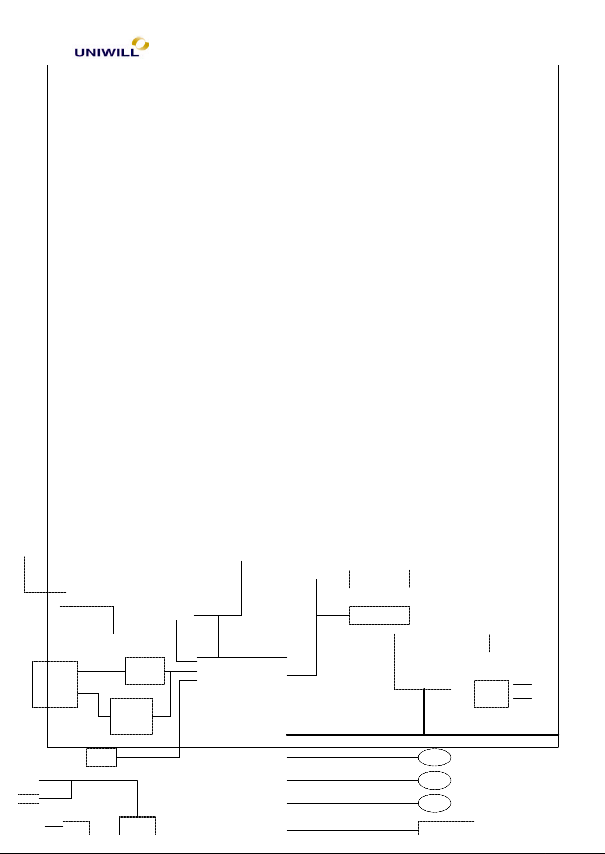
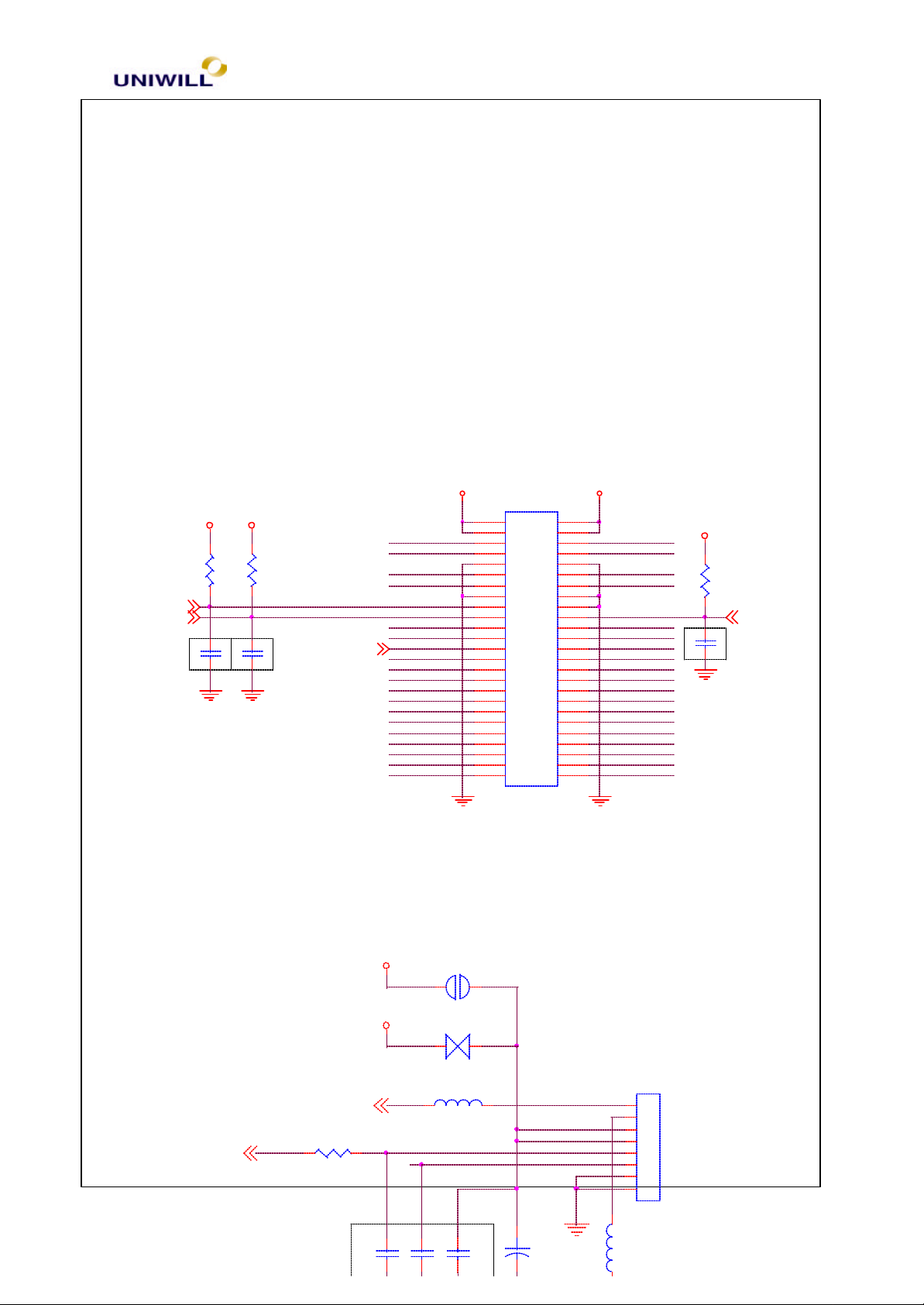
1.2 System Specification
1.2.1 System Board
The major components of the computer include the system board, XGA color LCD
display, FDD module,CD-ROM module (24X rotational speed max) / DVD
module, keyboard, built-in glide pad with 2 click buttons, Lithium-ION battery
pack, and AC adapter.
The system board incorporates CPU module, system memory, system and VGA
BIOS, audio controller, CPU/ PCI bus controller, PCI / ISA bus controller. The
System Block Diagram shows how these components are integrated as shown in
the next page.
CPU_CORE
2.5V
1.5V
VCC_CMOS
CPU
Celeron PPGA
Pentium !!! FC-PGA
LVDS
TRANSCEIVER
THC63LVDF63
DSTN ENCODER
NS CS9211
CORE LOGIC
CRT PORT
340S2 4 Rev : B
AC97 CODECAUDIO
SIS630
SO-DIMM1
SO-DIMM2
PCI BUS
CARDBUS
OZ6812
CD-ROM
HDD
USB
RJ-45 CONNECTOR
CARDBUS SOCKET
SOCKET
POWER
MIC2562A
VCCSKT
VPPSKT
Page 5

Chapter 1 General System Description
1.2.2 LCD Display
14.1” TFT
13.3” TFT
12.1” TFT
13.0” HPA
12.1” HPA
1.2.3 Power Plans
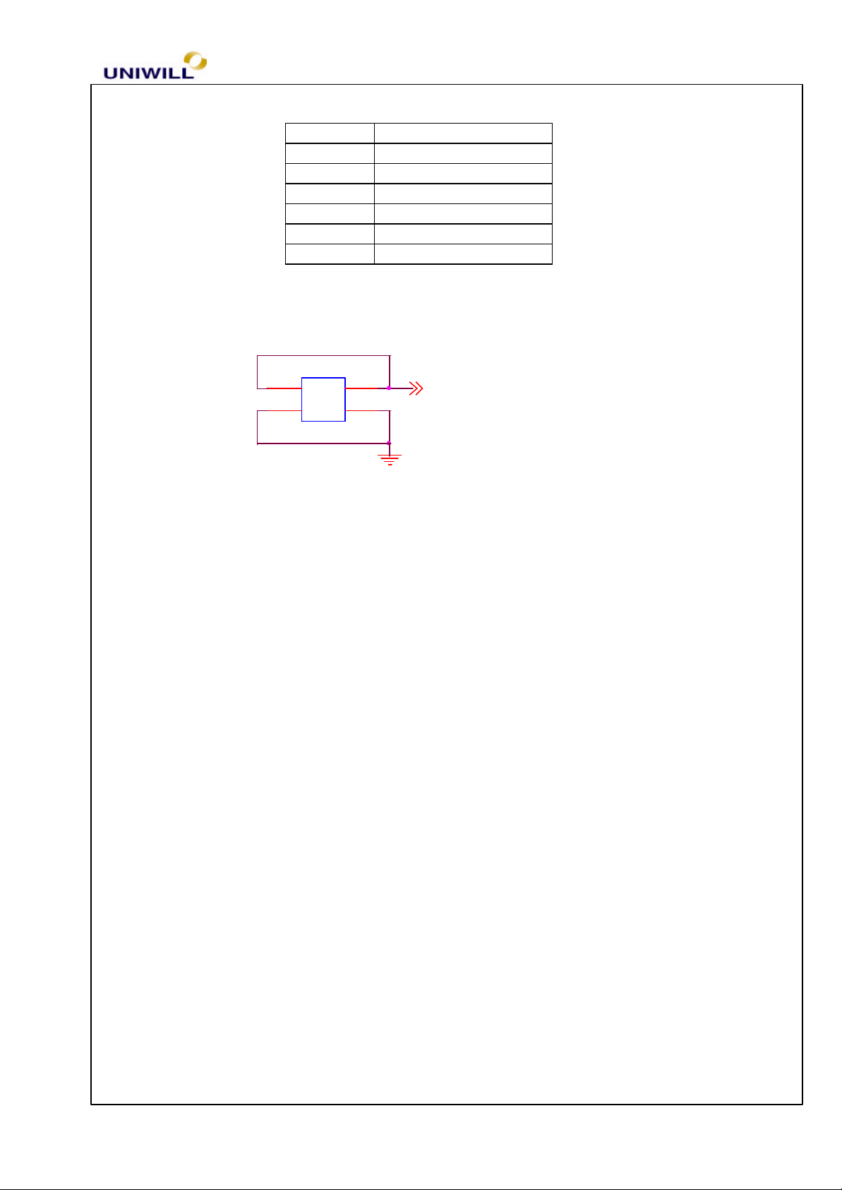
Power Source Descriptions
+5V : 5V power source
+3V : 3.3V power source
+12V : 12V power source
CPU_Core : CPU Core power source.
For Celeron, the voltage is 2.0V.
For Pentium III, it is 1.8V.
+1.5V : CPU AGTL+ termination power source
VCC_CMOS : CPU CMOS pull up voltage.
For Celeron, the voltage is 2.5V.
For Pentium III, it is 1.5V.
+2.5V : 2.5V power source
+1.8V : 1.8V power source for SIS630
KBVCC : KBC 3.3V power source
KBVCCA : KBC AD/DA 3.3V reference voltage
VCCRTC : Real time clock power source
+5V_AUX : LAN 5V always power source
+3V_AUX : LAN 3.3V always power source
+3V_RX_TR : LAN 3.3V analog power source
+3V_TX_TR : LAN 3.3V analog power source
LCDVCC : LCD display 3.3V power source
VIN : Inverter 12~20V power source
ADAP+ : 20V Power supply from AC adapter
AMPVDD : 5V analog power for audio
340S2 5 Rev : B
Page 6

Chapter 1 General System Description
340S2 6 Rev : B
Page 7
Chapter 1 General System Description
1.2.4 Power Source Status
5V 3.3V 12V CPU
_core
FULL-ON ON ON ON ON ON ON ON ON
SLEEP ON ON ON ON ON ON ON ON
STD OFF OFF OFF OFF OFF OFF OFF OFF
SOFT-OFF OFF OFF OFF OFF OFF OFF OFF OFF
1.2.5 DC/DC Board
The DC/DC (system power) can support +3.3V, +5V, +12V for the main system.
The DC/DC (CPU power) can support +1.3V~2.05V, +1.8V, +2.5V for the CPU.
VCC_
CMOS
2.5V 1.5V 1.8V
1.2.6 AC-DC Adapter
Input Voltage : 100 ~ 240 ±10% AC
Input Frequency : 50 ~ 60 Hz ±3Hz
Input AC current : 1.5 @ 90 VAC
Efficiency : Better than 80%
Inrush Current : 50A @ 115VAC, 100A @ 230VAC
Holdup Time : 5mS (minimum)
Output Voltage/Current : 20V / 3.0A
Output Load Regulation : ±5%
1.2.7 Inverter
Input Voltage : 9-22 VDC
Output Voltage : 620 Vrms @ 50-60KHz
Start Up Voltage : 1400 Vrms (min.)
Brightness Adjust Range (tube current) : 2.5mA rms – 5mA rms
Protection : Open circuit protect, current limit protect
1.2.8 Battery Pack
A. Lithium – Ion Battery packs
• Battery type : Li-Ion
• Battery cells : 8 cells
340S2 7 Rev : B
Page 8
Chapter 1 General System Description
• Battery Spec : 14.8V, 3200 mAH
• Battery power : 53 watts (total)
• Battery protection : over charge protect, over discharge protect, over
temperature protect, short protect, over current protect
B. Ni-MH battery packs
• Battery type : Ni MH
• Battery cells : 10 cells
• Battery specs : 12V, 4500 mAh
• Battery power : 54 watts (total)
• Battery protection : over charge protect, over discharge protect, over
temperature protect, short protect, over current protect
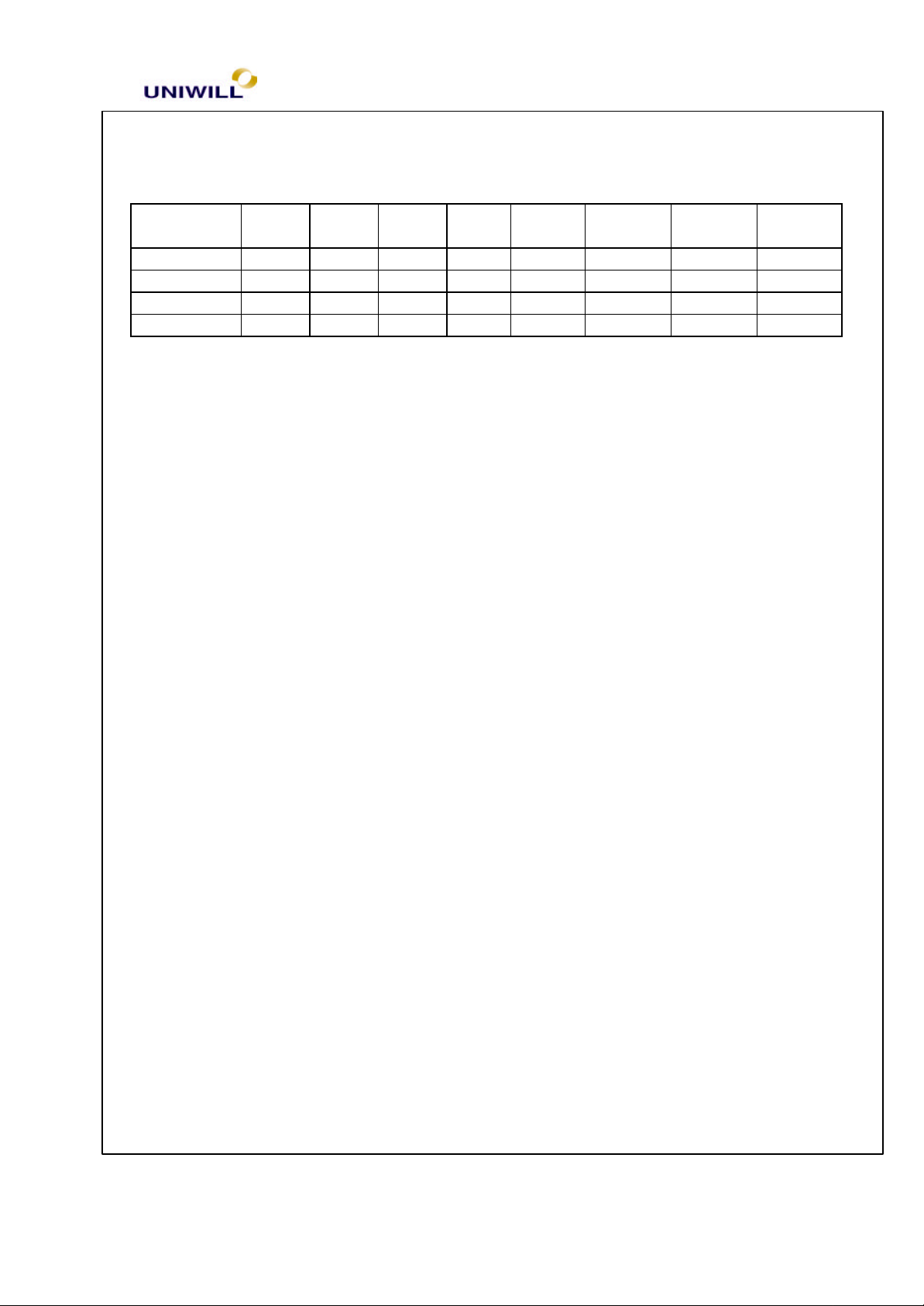
1.2.9 Memory Module
144 pins SO-DIMM, 3.3V, SDRAM
memory type = 1Mx16, 4Mx16, 16Mx16, 2Mx8, 8Mx8, 16Mx8
memory size = 16M, 32M, 64M, 128M,
memory clock = 66 MHz / 100MHz
Memory Configuration Table
DIMM 1 DIMM 2 Total
16M 0 16M
32M 0 32M
64M 0 64M
128M 0 128M
16M 16M 32M
16M 32M 48M
32M 32M 64M
16M 64M 80M
32M 64M 96M
64M 64M 128M
64M 128M 192M
128M 128M 256M
340S2 8 Rev : B
Page 9
Chapter 1 General System Description
1.2.10 Interrupt Request Channel
Setting Hardware using the setting
00 System timer
01 Standard 101/102-Key Microsoft Natural Keyboard
02 Programmable Interrupt Controller
03 IrDA V3.0 Fast Infrared Port
04 Communications Port (Com1)
06 Stan dard Floppy Disk Controller
07 ECP Printer Port (LPT1)
08 System CMOS/ Real Time Clock (RTC)
09 ACPI IRQ Holder for PCI IRQ Steering
09 SiS 900 PCI Fast Ethernet Adapter
10 ACPI IRQ Holder for PCI IRQ Steering
10 HAMR 5600 Voice Modem
10 O2Micro OZ6812 CardBus Controller
10 SIS 7018 Audio Driver
11 ACPI IRQ Holder for PCI IRQ Steering
11 SIS 7001 PCI to USB Open Host Controller
11 SIS 7001 PCI to USB Open Host Controller
11 SCI IRQ used by ACPI bus
12 Microsoft PS/2 Port Mouse
13 Numeric data processor
14 SIS 5513 Dual PCI IDE Controller
14 Primary IDE Controller (dual FIFO)
15 Intel 82371AB/EB PCI Bus Master IDE Controller
15 Secondary IDE Controller (dual FIFO)
1.2.11 DMA Channel
Setting Hardware using the setting
01 IrDA V3.0 Fast Infrared Port
02 Standard Floppy Disk Controller
03 ECP Printer Port (LPT1)
04 Direct memory access controller
340S2 9 Rev : B
Page 10
Chapter 2 Connectors & Switches
Rev : B
1.2.12 System LED Indicator
4 Num-lock (on/off)
4 Cap-lock (on/off)
4 Scroll-Lock (on/off)
4 FDD (on/off)
4 HDD (on/off)
4 CDROM (on/off)
4 Power (on/off)
When the system is powered on, the Power LED will be lighted on.
When ‘Battery Low Warning’ occurs, the Power LED will flash at a rate of
1 time every 16 second.
When ‘Battery Very Low Warning’ occurs, the Power LED will flash at a
rate of 1 time every 4 seconds if there is no ‘Suspend to Disk’ partition in
the hard disk.
4 Charge (flash/off): Will be flashing when the battery pack is being charged.
1.2.13 Hot Key:
Key combination Function
Fn + F1 Standby Mode
Fn + F3 Mute battery warning beep
Fn + F4 Toggle LCD / CRT display
Fn + F5 Volume increase
Fn + F6 Volume decrease
Fn + F7 Brightness up
Fn + F8 Brightness down
Fn + F9 Contrast up (for DSTN LCD)
Fn + F10 Contrast down(for DSTN LCD)
340S2 10
Page 11

Chapter 2 Connectors & Switches
Rev : B
UNIWILL COMPUTER CORP.
No. 24 Pei Yuan Road
Chung Li Industrial Park, Chung Li City
Tao Yuan Hsien, Taiwan,
R.O.C.
TEL: 886-3-461-6000
FAX: 886-3-461-6317
URL: http:// www.uniwill.com.tw/
340S2 11
Page 12
Chapter 2 Connectors & Switches
Rev : B
DIMM144
DIMM144-REV
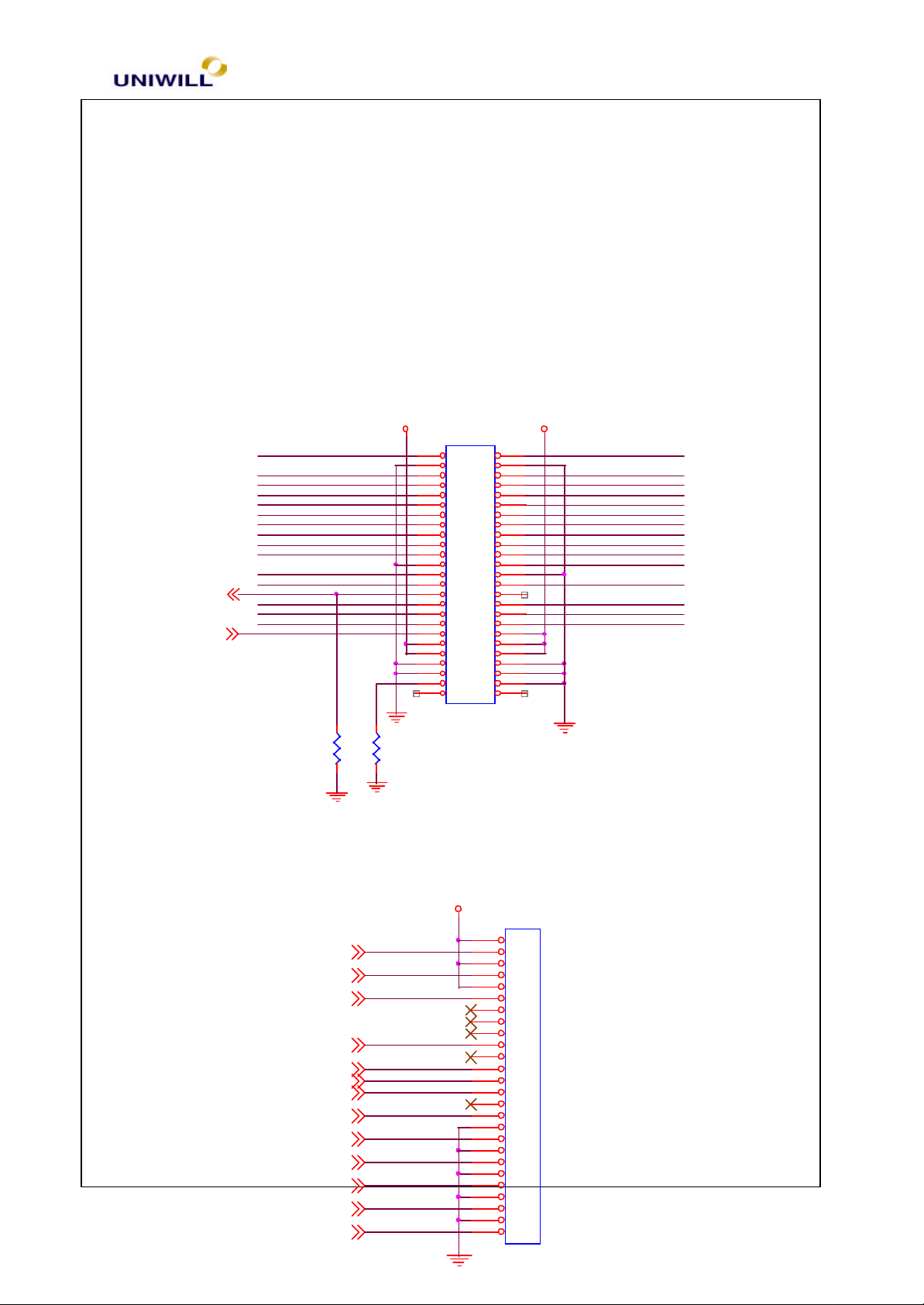
2.1 Connector Definitions
2.1.1 Memory DIMM144 Connector (CN7 and CN6)
2.1.2 Modem/B Connector (CN29)
340S2 12
121
123
125
127
131
133
135
137
115
117
116
118
141
142
101
102
113
114
129
130
143
144
3
5
7
9
13
15
17
19
37
39
41
43
47
49
51
53
83
85
87
89
93
95
97
99
23
25
24
26
69
71
67
73
11
12
27
28
45
46
63
64
81
82
61
74
62
68
65
66
T9
CN7
DQ0
DQ1
DQ2
DQ3
DQ4
DQ5
DQ6
DQ7
DQ8
DQ9
DQ10
DQ11
DQ12
DQ13
DQ14
DQ15
DQ16
DQ17
DQ18
DQ19
DQ20
DQ21
DQ22
DQ23
DQ24
DQ25
DQ26
DQ27
DQ28
DQ29
DQ30
DQ31
DQMB0/CAS0#
DQMB1/CAS1#
DQMB2/CAS2#
DQMB3/CAS3#
DQMB4/CAS4#
DQMB5/CAS5#
DQMB6/CAS6#
DQMB7/CAS7#
S0#/RAS0#
S1#/RAS1#
WE#
NU/OE#
SDA
SCL
VCC
VCC
VCC
VCC
VCC
VCC
VCC
VCC
VCC
VCC
VCC
VCC
VCC
VCC
VCC
VCC
VCC
VCC
CLK0
CLK1/RFU
CKE0/RFU
CKE1/RFU
SRAS#/RFU
SCAS#/RFU
AD0
AD1
AD2
AD3
AD4
AD5
AD6
AD7
AD8
DQ32
DQ33
DQ34
DQ35
DQ36
DQ37
DQ38
DQ39
DQ40
DQ41
DQ42
DQ43
DQ44
DQ45
DQ46
DQ47
DQ48
DQ49
DQ50
DQ51
DQ52
DQ53
DQ54
DQ55
DQ56
DQ57
DQ58
DQ59
DQ60
DQ61
DQ62
DQ63
A0
A1
A2
A3
A4
A5
A6
A7
A8
A9
A10
A11/BA0
A12/BA1
A13/A11
RFU/A12
RFU/A13
NC/CB0
NC/CB1
NC/CB2
NC/CB3
NC/CB4
NC/CB5
NC/CB6
NC/CB7
VSS
VSS
VSS
VSS
VSS
VSS
VSS
VSS
VSS
VSS
VSS
VSS
VSS
VSS
VSS
VSS
VSS
VSS
CN29
1 2
3 4
5 6
7 8
9 10
11 12
13 14
15 16
17 18
19 20
21 22
23 24
25 26
100
122
124
126
128
132
134
136
138
103
104
105
109
111
106
110
112
107
108
119
120
139
140
CN6
4
6
8
10
14
16
18
20
38
40
42
44
48
50
52
54
84
86
88
90
94
96
98
29
31
33
30
32
34
70
72
57
59
77
79
58
60
78
80
1
2
21
22
35
36
55
56
75
76
91
92
PERR#
SERR#
FRAME#
IRDY#
TRDY#
DEVSEL#
AD16
STOP#
PAR
INT#A
3
5
7
9
13
15
17
19
37
39
41
43
47
49
51
53
83
85
87
89
93
95
97
99
121
123
125
127
131
133
135
137
23
25
115
117
24
26
116
118
69
71
67
73
141
142
11
12
27
28
45
46
63
64
81
82
101
102
113
114
129
130
143
144
61
74
62
68
65
+5V+3V KBVCC
66
PERR# 13
DQ0
DQ1
DQ2
DQ3
DQ4
DQ5
DQ6
DQ7
DQ8
DQ9
DQ10
DQ11
DQ12
DQ13
DQ14
DQ15
DQ16
DQ17
DQ18
DQ19
DQ20
DQ21
DQ22
DQ23
DQ24
DQ25
DQ26
DQ27
DQ28
DQ29
DQ30
DQ31
DQMB0/CAS0#
DQMB1/CAS1#
DQMB2/CAS2#
DQMB3/CAS3#
DQMB4/CAS4#
DQMB5/CAS5#
DQMB6/CAS6#
DQMB7/CAS7#
S0#/RAS0#
S1#/RAS1#
WE#
NU/OE#
SDA
SCL
VCC
VCC
VCC
VCC
VCC
VCC
VCC
VCC
VCC
VCC
VCC
VCC
VCC
VCC
VCC
VCC
VCC
VCC
CLK0
CLK1/RFU
CKE0/RFU
CKE1/RFU
SRAS#/RFU
SCAS#/RFU
DQ32
DQ33
DQ34
DQ35
DQ36
DQ37
DQ38
DQ39
DQ40
DQ41
DQ42
DQ43
DQ44
DQ45
DQ46
DQ47
DQ48
DQ49
DQ50
DQ51
DQ52
DQ53
DQ54
DQ55
DQ56
DQ57
DQ58
DQ59
DQ60
DQ61
DQ62
DQ63
A0
A1
A2
A3
A4
A5
A6
A7
A8
A9
A10
A11/BA0
A12/BA1
A13/A11
RFU/A12
RFU/A13
NC/CB0
NC/CB1
NC/CB2
NC/CB3
NC/CB4
NC/CB5
NC/CB6
NC/CB7
VSS
VSS
VSS
VSS
VSS
VSS
VSS
VSS
VSS
VSS
VSS
VSS
VSS
VSS
VSS
VSS
VSS
VSS
100
122
124
126
128
132
134
136
138
103
104
105
109
111
106
110
112
107
108
119
120
139
140
4
6
8
10
14
16
18
20
38
40
42
44
48
50
52
54
84
86
88
90
94
96
98
29
31
33
30
32
34
70
72
57
59
77
79
58
60
78
80
1
2
21
22
35
36
55
56
75
76
91
92
Page 13
Chapter 2 Connectors & Switches
Rev : B
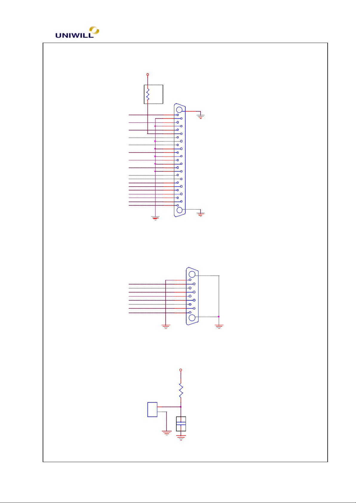
2.1.3 LCD Connector (CN4)
R302
10K
C363
C
+3V+3V
R297
10K
C344
CONTRAST18
C
PNLSW05
PNLSW15
2.1.4 Inverter Connector (CN3)
+5V
VIN
INT_MIC12
BLTADJ18
R281 0
340S2 13
C325
LCDVCC LCDVCC
Y0+ Y1+
Y2-
Y2+
FFPHSYNC
LLD10
UUD0
UUD4
LLD8
LLD0
LLD2
LLD4
LLD6
UUD2
UUD6
UUD8
UUD10
1 2
OPEN_S
J4
1 2
CLOSE_S
L55 0
DISPON
C321
C
C
J3
C328
C
CN4
1
3
5
7
9
10
11
12
13
14
15
16
17
18
19
20
21
22
23
24
25
26
27
28
29
30
31
32
33
34
35
36
37
38
39
40
41
42
43
44
45
46
47
48
49
50
LCD CONN
12
+ C23
1u/25V_0805
2
4
6
8
Y1-Y0-
CLKCLK+
FFPSHFCLK
FFPVSYNCENBLT
FFPDE
LLD11
UUD1
UUD5
LLD9
LLD1
LLD3
LLD5
LLD7
UUD3
UUD7
UUD9
UUD11
CN3
1
2
3
4
5
6
7
8
L54
BLM11P600S
INVERTER
+3V
R13
10K
PNLSW2 5
C27
C
Page 14
Chapter 2 Connectors & Switches
Rev : B
RJ45
2.1.5 CRT Connector (CN20)
Pin Description Pin Description
1 RED 9 +5V
2 GREEN 10 GND
3 BLUE 11 NC4 NC 12 DDCCLK
5 GND 13 HSYNC
6 DACGND 14 VSYNC
7 DACGND 15 DDCDATA
8 DACGND
2.1.6 USB Connector (CN21)
Pin Description
1 +5V
2 USBP03 USBP0+
4 GND
2.1.7 RJ45 (CN15)
8
7
6
5
4
3
2
1
CN15
NC4
NC3
RONC2
NC1
RO+
TDTD+
GND
GND
10
2.1.8 RJ11 (CN16)
Pin Description
1 HRTXRXN
2 HRTXRXP
9
340S2 14
Page 15
Chapter 2 Connectors & Switches
Rev : B
MICGND
2.1.9 Modem Phone (CN17) and Modem Connector (CN23)
CN17
1
2
MODEM-PHONE
2.1.10 MDC Connector (CN26)
SDATO5,12
AC_RESET#5,12
PCIRST#4,9,12,13,14,15
MDCLK12
R204 0
R203 R
2.1.11 MIC Jack (CN13)
INT_MIC8
2.1.12 Speaker Jack (CN12)
340S2 15
1
1
RV1
2
2
DSSA P3100SBRP
+3V
AMPVDD
AMPVDD
1000p/2KV_1808
1
MONO_OUT
3
GND
5
AUXR
7
AUXL
9
CDGND
11
CD_R
13
CD_L
15
GND
17
3.3V
19
GND
21
3.3V
23
SDATA_O
25
RESET#
27
GND
29
MCLK
VREFOUT
R266
100K
EXTSPKR
EXTSPKHP
EXTSPKL
R276
100K
R268
10K
R269
10K
R279
10K
R278
10K
C327
CN26
AUDIO_PD
MONO_PHONE
R_D
GND
VCC
R_D
R_D
P_DN
VCC
GND
SYNC
SDATA_INB
SDATA_INA
GND
BCLK
MDC CON.
C315
0.1u
C308
680p
CN12
5
4
3
2
1
SPKR JACK
L30
BLM11P600S
C317
1000p/2KV_1808
+5V
2
4
6
8
10
12
14
16
18
20
22
24
26
28
30
CN13
5
4
3
2
1
MIC JACK
L26
BLM11P600S
MODEM CONN
R198 R
R195 0
R194 0
CN23
1
2
PHONE 12
MODEMRI# 17
SYNC 5,12
SDATIN1 5
SDATIN0 5,12
BIT_CLK 5,12
+3V
R196
R
R197
0
Page 16
Chapter 2 Connectors & Switches
Rev : B
PCMCIA CONN
2.1.13 R/L Speaker Connector (CN5)
2.1.14 PCMCIA Connector (CN28)
2.1.15 HDD Connector (CN27)
340S2 16
L61 BLM21300S_0805
L60 BLM21300S_0805
L58 BLM21300S_0805
L57 BLM21300S_0805
CN28
51
VCC
17
VCC
52
VPP
18
VPP
19
CCLK (A16)
54
CFRAME# (A23)
20
CIRDY# (A15)
53
CTRDY# (A22)
50
CDEVSEL# (A21)
49
CSTOP# (A20)
13
CPAR (A13)
14
CPERR# (A14)
59
CSERR# (WAIT*)
60
CREQ# (INPACK*)
15
CGNT# (WE*)
16
CINT# (IRQ*)
48
CBLOCK# (A19)
33
CCLKRUN# (IO16*)
58
CRESET# (RESET)
32
RFU (R2_D2)
40
RFU (R2_D14)
47
RFU (R2_A18)
43
CVS1
57
CVS2
36
CCD1# (CD1*)
67
CCD2# (CD2*)
62
CAUDIO (BVD2/SPKR*)
63
CSTSCHG (BVD1/RI*)
61
CC/BE3# (REG*)
21
CC/BE2# (A12)
12
CC/BE1# (A8)
7
CC/BE0# (CE1*)
HDDRST#
PIDED7
PIDED6
PIDED5
PIDED4
PIDED3
PIDED2
PIDED1
PIDED0
PIDEDREQ
PIDEIOW#
CN27
1 2
3 4
5 6
7 8
9 10
11 12
13 14
15 16
17 18
19 20
21 22
23 24
(D10) CAD31
(A25) CAD19
(A24) CAD17
(A17) CAD16
(IOWR*) CAD15
(IORD*) CAD13
(A11) CAD12
(OE*) CAD11
(CE2*) CAD10
RR+
L+
L-
(D9) CAD30
(D1) CAD29
(D8) CAD28
(D0) CAD27
(A0) CAD26
(A1) CAD25
(A2) CAD24
(A3) CAD23
(A4) CAD22
(A5) CAD21
(A6) CAD20
(A7) CAD18
(A9) CAD14
(A10) CAD9
(D15) CAD8
(D7) CAD7
(D13) CAD6
(D6) CAD5
(D12) CAD4
(D5) CAD3
(D11) CAD2
(D4) CAD1
(D3) CAD0
GND
GND
GND
GND
V_HDDV_HDD
CN5
4
3
2
1
R/L SPKR CONN
66
65
31
64
30
29
28
27
26
25
24
23
56
22
55
46
45
11
44
10
9
42
8
41
6
39
5
38
4
37
3
2
68
35
34
1
PIDED8
PIDED9
PIDED10
PIDED11
PIDED12
PIDED13
PIDED14
PIDED15
Page 17
Chapter 2 Connectors & Switches
Rev : B
FDD CONN
2.1.16 CDROM Connector
IRQ154
CD-ROMLED#17
SIDECDL
CDRST#
SIDED7
SIDED6
SIDED5 SIDED11
SIDED4
SIDED3 SIDED13
SIDED2 SIDED14
SIDED1
SIDED0
SIDEIOW#
SIORDY
SIDEA1
SIDEA0
SIDECS1#
2.1.17 FDD Connector (CN10)
INDEX#15
DRV0#15,17
DSKCHG#15
340S2 17
MTR0#15
FDIR#15
3MODE#5,15
STEP#15
WDATA#15
WGATE#15
TRK0#15
WRPRT#15
RDATA#15
HDSEL#15
V_CDROM V_CDROM
R498
10K
R57
0
INDEX#
DSKCHG#
TRK0#
WRPRT#
RDATA#
CDROM CONN
Secondary
Drive(Master)
V_FDD
CN24
1 2
3 4
5 6
7 8
9 10
11 12
13 14
15 16
17 18
19 20
21 22
23 24
25 26
27 28
29 30
31 32
33 34
35 36
37 38
39 40
41 42
43 44
45
47
49
SIDECDR
SIDED8
SIDED9
SIDED10
SIDED12
SIDED15
SIDEDREQ
SIDEIOR#
SIDEDACK#
S66CBLIDB
SIDEA2
SIDECS3#
46
48
50
CN10
1
2
3
4
5
6
7
8
9
10
11
12
13
14
15
16
17
18
19
20
21
22
23
24
25
26
Page 18

Chapter 2 Connectors & Switches
Rev : B
340S2 18
Page 19
Chapter 2 Connectors & Switches
Rev : B
PARALLEL CONN
2.1.18 Parallel Connector (CN18)
+5V
LPTSLCT
LPTPE
LPTBUSY
LPTACK#
LPTD7
LPTD6
LPTD5
LPTD4
LPTD3
LPTSLCTIN#
LPTD2
LPTINIT#
LPTD1
LPTERR#
LPTD0
LPTAFD#
LPTSTB#
R253
R
CN18
13
25
12
24
11
23
10
22
9
21
8
20
7
19
6
18
5
17
4
16
3
15
2
14
1
2.1.19 Serial Connector (CN19)
COMRI1
COMDTR1#
COMCTS1#
COMTXD1
COMRTS1#
COMRXD1
COMDSR1#
COMDCD1#
CN19
5
9
4
8
3
7
2
6
1
SERIAL CONN
26
27
10
11
2.1.20 LID Connector (CN1)
340S2 19
CN1
LID CONN
+3V
R12
100K
LID
1
2
C22
C
Page 20
Chapter 4 System Disassembly
Rev : B
INT KB CONN
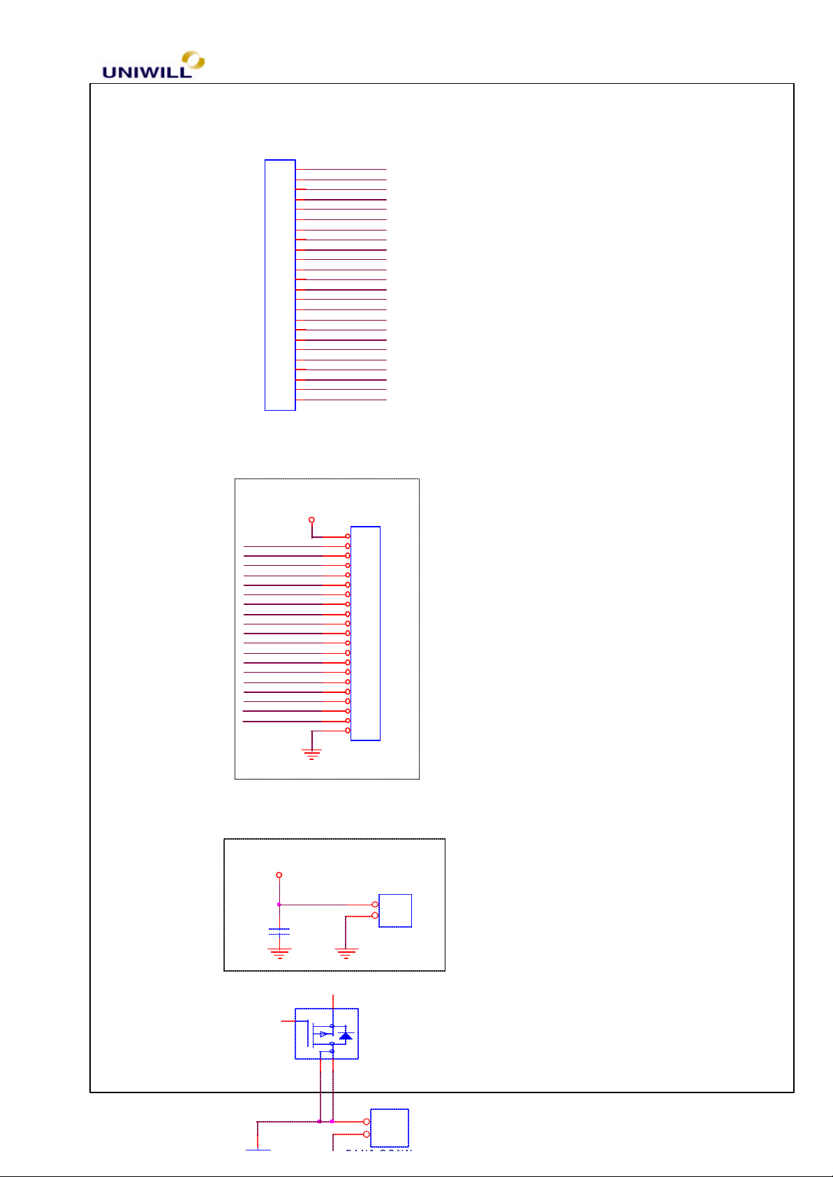
2.1.21 Internal KB Connector (CN9)
2.1.22 Test Connector (CN8)
2.1.23 Fan2 Connecto r (CN2)
2.1.24 Fan1 Connector (CN25)
CN9
ROMA0
ROMA1
ROMA2
ROMA3
ROMA4
ROMA5
ROMA6
ROMA7
ROMD0
ROMD1
ROMD2
ROMD3
ROMD4
ROMD5
ROMD6
ROMD7
TEST
ROMRD#
ROMWR#
+5V
24
23
22
21
20
19
18
17
16
15
14
13
12
11
10
9
8
7
6
5
4
3
2
1
2
KBVCC
C303
C
SCANIN0
SCANIN1
SCANOUT1
SCANOUT2
SCANIN4
SCANIN5
SCANIN6
SCANOUT0
SCANIN7
SCANIN2
SCANIN3
SCANOUT3
SCANOUT4
SCANOUT5
SCANOUT6
SCANOUT7
SCANOUT8
SCANOUT9
SCANOUT10
SCANOUT11
SCANOUT12
SCANOUT13
SCANOUT14
SCANOUT15
CN8
1
2
3
4
5
6
7
8
9
10
11
12
13
14
15
16
17
18
19
20
21
TEST CONN
FAN2 CONN
1
7
8
2
1
Q41A
SI9953
CN2
340S2 20
C476
CN25
2
1
Page 21
Chapter 4 System Disassembly
Rev : B
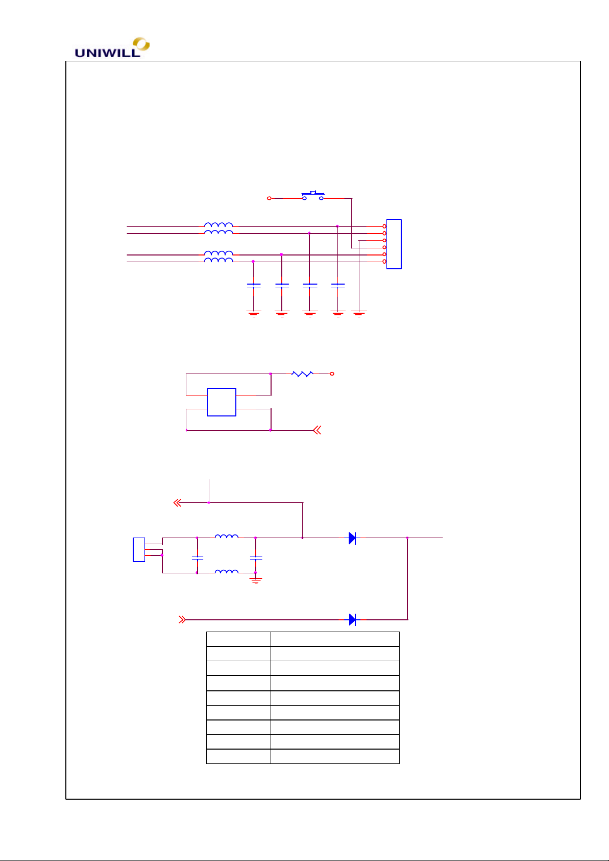
2.1.25 PS2 Connector (CN14)
KBDATA
PS2DATA
KBCLK
PS2CLK
L50 BLM11P600S
L24 BLM11P600S
L52 BLM11P600S
L1
BLM11P600S C304
2.1.26 Power Switch (SW2)
SW2
1 2
3 4
POWER SW
2.1.27 AC Connector (CN22)
CN22
1
2
3
AC CONN
ADAP_IN18,23
L53
BLM21300S_0805
C306
10u/25V_1210
BLM21300S_0805
L74
2.1.28 Battery Connector (CN30)
BATT+21,23
Pin No. Pin Name
2.1.29 Touch Pad Connector (CN11)
+5V
POLY SW_1812
C14
270p
270p
ADAP+
C331
10u/25V_1210
1 BATT+
2 SMBCLK
3 SMBDATA
4 TEMP
5 +5V_AUX
6 GND
7 NC
8 NC
R18
10K
S2
C305
C316
270p
270p
+5V_AUX
PWRSW 22
D25
SR34
A C
D26
SR54
ANODECATHODE
CN14
1
2
3
4
5
6
PS2 CONN
340S2 21
Page 22
Chapter 4 System Disassembly
Rev : B
Pin No. Pin Name
1 PSCLK3
2 PSDAT3
3 GND
4 NC
5 +5V
6 NC
2.1.30 But_SW_0 (SW1)
2.2 Mechanical Buttons and Switch Definition
2.2.1 Power on/off button
1. If the system is in S0, S1 or S2 state, pressing the power button will transit the
system to S4 (Suspend to Disk), S5 (Soft-off) state depending on the “Power button
function” setting in the BIOS Setup menu.
2. If the system is in S4 or S5 state, pressing the power button will awaken the system
into S0 state.
3. If the power button is pressed for more than four seconds, a power button over-ride
event is generated and the system will be put into S5 (Soft-off) state.
2.2.2 Cover (Lid) Switch
When LCD cover is closed, this Lid switch is triggered and an SMI/SCI is generated to
put the system into ‘Suspend to RAM’ or ‘Suspend to Disk’ mode depending on the
“Cover Switch” setting in the BIOS Setup menu.
2.2.3 WWW function button
SW1
1 2
3 4
BUT-SW_0
FUNCSW# 18
340S2 22
Page 23

Chapter 4 System Disassembly
Rev : B
When this button is pressed, the system will launch Microsoft Internet Explorer and
connect to default setting of Internet Explorer.
2.2.4 CPU DIP Switch Settings (SW7 – near CPU socket)
SW7 (For Celeron and Pentium III)
1 2 3 4 CPU SDRAM
ON OFF OFF OFF 66M 66M
OFF OFF OFF OFF 66M 100M
OFF OFF OFF ON 100M 100M
Note: SW7-5, 6, 7, 8: Always OFF
Celeron
Processor System Bus Frequency(MHz) L2 Cache Size(Kbytes)
500 66 128
533 66 128
566 66 128
600 66 128
Pentium III
Processor System Bus Frequency(MHz) L2 Cache Size(Kbytes)
500 100 256
550E 100 256
600E 100 256
650 100 256
700 100 256
750 100 256
800 100 256
850 100 256
340S2 23
Page 24
Chapter 4 System Disassembly
Rev : B
U10
U33
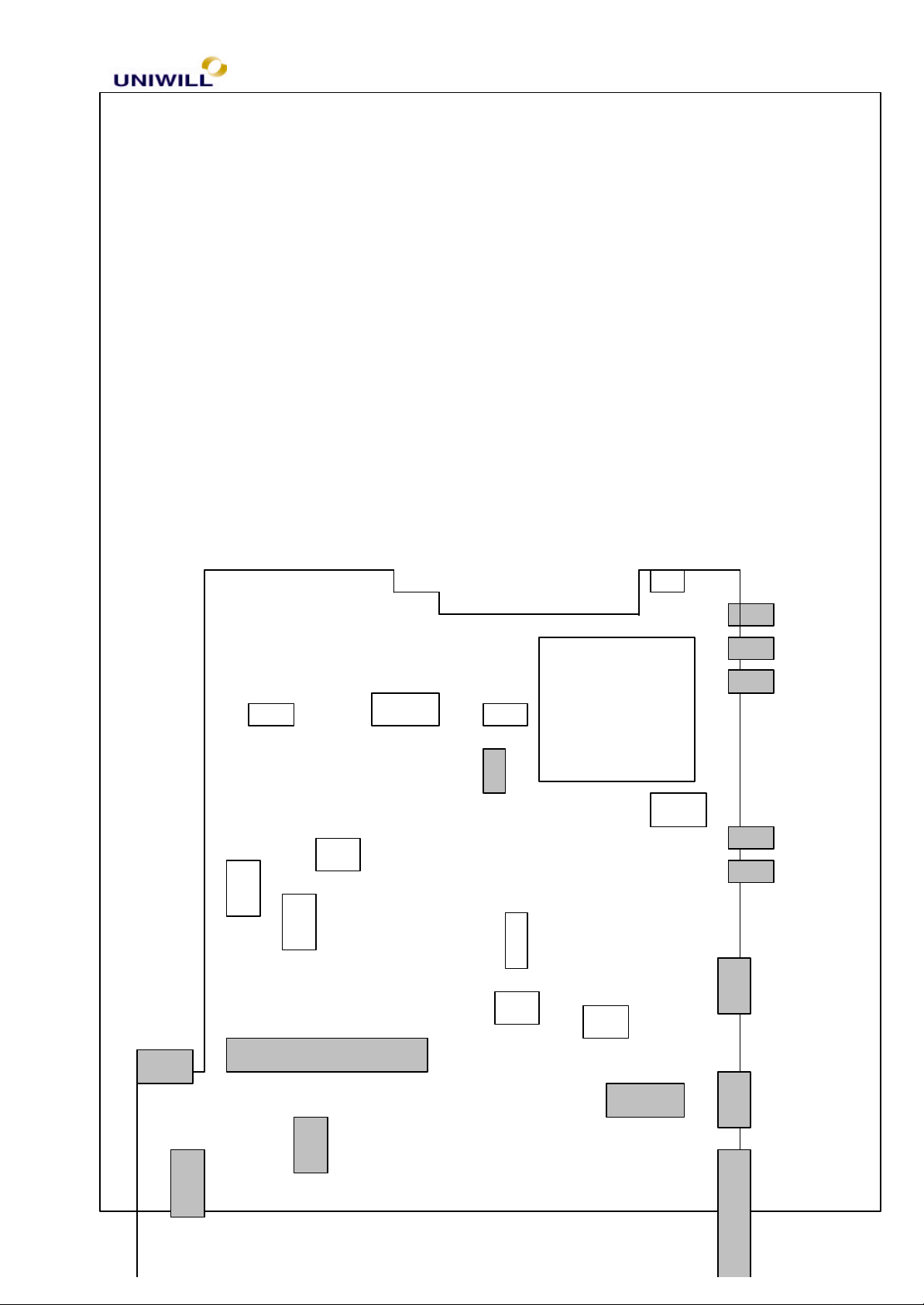
2.3. Major Components and Connectors Location
2.3.1 Bottom Side
U47
U42
U37
U43
CN30
CN27
CN29
CN26
U45
CN25
SW 7
U36
U13
U35
CN24
IR1
CN21
CN17
CN14
CN13
CN12
CN20
CN19
340S2 24
CN18
Page 25
Chapter 4 System Disassembly
Rev : B
U19
U20
U2
U3
U4 U9
2.3.2 Top Side
CN1
U1
CN3
CN28
CN5
SW2
U7 U6
SW1
CN4
U15
CN7
U8
U12 U17
U25
CN6
U26
CN15
U44
U21
CN10
U31
U29
U28
CN9
U32
CN11
340S2 25
Page 26
Chapter 4 System Disassembly
Rev : B
U11
U14
U18
UNIWILL COMPUTER CORP.
No. 24 Pei Yuan Road
Chung Li Industrial Park, Chung Li City
Tao Yuan Hsien, Taiwan,
R.O.C.
TEL: 886-3-461-6000
FAX: 886-3-461-6317
URL: http:// www.uniwill.com.tw/
340S2 26
Page 27
Chapter 4 System Disassembly
Rev : B
3.1 Major Component List
Reference
U1 RS-232 TRANSCEIVER ANALOG ADM213
U2 P-MOSFET FOR LCD VCC CET 9424 SO -8
U3 1MX16 VRAM - NT56V1616A0T
U4 LVDS PANEL TRANSMITTER TI SN75LVDS84
U6 NOT GATE TI 74LVC14
U7 AND GATE PHILIPS 74LVC08
U8 OR GATE - 74LVC32
U9 4MX16 VRAM HYUNDAI M12L1616A_7T
U10 CLOCK GENERATOR WINBOND
U11 SUPER I/O CONTROLLER NS PC87393
U12 DSTN CONTROLLER NS CS9211
U13 SERIAL ROM FOR LAN ATMEL 93C46
U14 SWITCH TI 74LVC373
U15 CORE LOGIC SIS SIS630
U17 BIOS EEPROM SOCKET UNICORN 29LV020(PLCC-32)
U18 KB CONTROLLER NS PC87570
U19 PWM CONTROL TI TL594-SOP16
U20 STEP DOWN DC-DC CONVERTER TOYOTA SB3060P-SSOP24
U21 LOW DROPOUT REGULATOR ALPHA AS2951
U24 ZENER SHUNT REGULATOR ZETEX ZR431
U25 AC’97 AUDIO CODEC AVANCE AVANCE_ALC100
U26 AUDIO AMPLIFIER NS LM4835
U28 RAM SWITCH PHILIPS 74HCT4066
U29 PCMCIA POWER CONTROLLER MICREL MIC2562A
U31 PCMCIA CONTROLLER O2Micro OZ6812
U32 OP AMP. NS LM358
U33 TEMPERATURE SENSOR AD ADM1021
U35 PPGA CPU SOCKET SKT SOCKET 370
U36 OCTAL BUFFER PHILIPS 74VLC244
U37 PWM CONTROL TI TL594
U42 LINEAR REGULATOR NS 78L12
U43 STEP DOWN DC-DC CONVERTER SMD SB3052P
U44 PWM CONTROL TI TL594
U45 LOW DROPOUT REGULATOR OMA AME8800DEFT
U47 LOW DROPOUT REGULATOR OMA AME8800AEFT
IR1 IR TRANSCEIVER MODULE STANLEY HRM230S
3.2 Major Components Pin Assignment
Description Vendor Component Name
ICS9248-126
340S2 27
Page 28

Rev : B
Y33
GND/CLKREF
C37
CPUPRES#
AL31
THERMDP
AL29
THERMDN
AH28
THERMTRIP#
W37
BCLK
AK20
LOCK#
AN19
DEFER#
AN25
TRDY#
AH4
RESERVED/RESET#
X4
RESET#/RESET2#
AN17
BPRI#
AN29
BREQ0#
AK28
RS#[2]
AH22
RS#[1]
AH26
RS#[0]
AN31
ADS#
AL23
HITM#
AL25
HIT#
AN27
DRDY#
AL27
DBSY#
AH14
BNR#
AL17
REQ#[4]
AL19
REQ#[3]
AH18
REQ#[2]
AH16
REQ#[1]
AK18
REQ#[0]
AF4
RESERVED/A#[35]
W3
RESERVED/A#[34]
AC1
RESERVED/A#[33]
X6
RESERVED/A#[32]
AD4
A#[31]
AA3
A#[30]
Z4
A#[29]
AK6
A#[28]
AA1
A#[27]
Y3
A#[26]
AF6
A#[25]
AB4
A#[24]
AB6
A#[23]
AE3
A#[22]
AJ1
A#[21]
AC3
A#[20]
AG3
A#[19]
Z6
A#[18]
AE1
A#[17]
AN7
A#[16]
AL5
A#[15]
AK14
A#[14]
AL7
A#[13]
AN5
A#[12]
AK10
A#[11]
AH6
A#[10]
AL9
A#[9]
AH10
A#[8]
AL15
A#[7]
AN9
A#[6]
AH8
A#[5]
AH12
A#[4]
AK8
A#[3]
Chapter 4 System Disassembly
1.1.1.1.1.SOCKET 370 _A
AK24
AN23
B36
W35
AM2
TESTHI
RESERVED/RP#
GND/RESERVED
RESERVED/AERR#
AC37
AL11
AN13
C31
C33
V4
RESERVED/BINIT#
RESERVED/BERR#
A33
RESERVED/AP0#
RESERVED/AP1#
RESERVED/RSP#
RESERVED/DEP1#
RESERVED/DEP0#
RESERVED/DEP2#
AK16
C29
E29
E31
A29
A31
RESERVED/DEP3#
AA33
RESERVED/VTT
RESERVED/DEP5#
RESERVED/DEP6#
RESERVED/DEP4#
RESERVED/DEP7#
AL13
AL21
AN11
AH20
AA35
RESERVED/VTT
RESERVED/VTT
RESERVED/VTT
RESERVED/VTT
RESERVED/VTT
RESERVED/VTT
AN15
AN21
E23
G35
S33
RESERVED/VTT
RESERVED/VTT
RESERVED/VTT
RESERVED/VTT
RESERVED/VTT
AK30
F10
S37
U35
U37
RESERVED
RESERVED
RESERVED/VTT
RESERVED/VTT
RESERVED/VTT
G37
L33
N33
N35
RESERVED
RESERVED
RESERVED
N37
Q33
Q35
Q37
RESERVED
RESERVED
RESERVED
RESERVED
Y1
E27
R2
S35
RESERVED
RESERVED
RESERVED
RESERVED
E21
X2
VCC_CMOS
RESERVED
RESERVED
VCORE-DET
BSEL1/GND
LINT[0]/INTR
LINT[1]/NMI
PWRGOOD
EDGCTRL/VRSEL
VCC_1.5V
VCC_2.5V
BPM#[0]
BPM#[1]
FLUSH#
IGNNE#
STPCLK#
PICCLK
BP#[2]
BP#[3]
BSEL#
A20M#
FERR#
IERR#
INIT#
SLP#
SMI#
PICD[0]
PICD[1]
PRDY#
PREQ#
TCK
TDI
TDO
TMS
TRST#
VID[3]
VID[2]
VID[1]
VID[0]
VREF7
VREF6
VREF5
VREF4
VREF3
VREF2
VREF1
VREF0
PLL1
PLL2
U35A
AD36
Z36
AB36
G33
E37
C35
E35
AJ33
AJ31
AE33
AC35
AE37
AE35
AG37
AG33
M36
L37
AH30
AJ35
AG35
J33
J35
L35
AK26
A35
J37
AL33
AN35
AN37
AK32
AN33
AJ37
AL37
AM36
AL35
AK22
AK12
AD6
F18
E33
AG1
W33
U33
V6
R6
K4
D#62
D#63
D#61
D#60
D#59
E25
F16
A27
A25
C17
C23
340S2 28
D#58
A19
D#57
C27
D#56
C19
D#55
C21
D#54
A23
D#53
D16
D#52
A13
D#51
C25
D#50
C13
D#49
A17
D#48
A15
D#47
A21
D#46
C11
D#45
A11
D#44
D#43A7D#42
D#41
D#40
D#39
D#38D8D#37A9D#36C9D#35B2D#34C7D#33C1D#32F6D#31C5D#30J3D#29A3D#28A5D#27
D12
D14
C15
D10
D#26E1D#25E3D#24K6D#23G3D#22F8D#21G1D#20L3D#19H6D#18P4D#17R4D#16H4D#15U3D#14N3D#13L1D#12Q1D#11M4D#10Q3D#9P6D#8S1D#7J1D#6T6D#5S3D#4U1D#3M6D#2N1D#1T4D#0
F12
W1
SOCKET_370
Page 29

Chapter 4 System Disassembly
Rev : B
SOCKET_370
1.1.1.1.2. SOCKET 370 B
GND
GND
GND
GND
GND
GND
GND
GND
GND
GND
GND
GND
GND
GND
GND
GND
GND
GND
GND
GND
GND
GND
GND
GND
GND
GND
GND
GND
GND
GND
GND
GND
GND
GND
GND
GND
GND
GND
GND
GND
GND
GND
GND
GND
GND
GND
GND
GND
GND
GND
GND
GND
GND
GND
GND
GND
GND
GND
GND
GND
GND
GND
GND
GND
GND
GND
GND
GND
GND
GND
GND
GND
GND
GND
GND
GND
GND
U35B
AC33
AD34
AH34
AM10
AM14
AM18
AM22
AM26
AM30
AM34
A37
AB32
AC5
AD2
AF32
AF36
AG5
AH2
AJ11
AJ15
AJ19
AJ23
AJ27
AJ3
AJ7
AK36
AK4
AL1
AL3
AM6
AN3
B12
B16
B20
B24
B28
B32
B4
B8
D18
D2
D22
D26
D30
D34
D4
E11
E15
E19
E7
F20
F24
F28
F32
F36
G5
H2
H34
K36
M2
M34
P32
P36
Q5
R34
T32
T36
U5
V2
V34
X32
X36
Y37
Y5
Z2
Z34
L5
AA37
AA5
AB2
AB34
AD32
AE5
AF2
AF34
AH24
AH32
AH36
AJ13
AJ17
AJ21
AJ25
AJ29
AJ5
AJ9
AK2
AK34
AM12
AM16
AM20
AM24
AM28
AM32
AM4
AM8
B10
B14
B18
B22
B26
B30
B34
B6
C3
D20
D24
D28
D32
D36
D6
E13
E17
E5
E9
F14
F2
F22
F26
F30
F34
F4
H32
H36
K2
K32
K34
M32
N5
P2
P34
R32
R36
S5
T34
V32
V36
W5
X34
Y35
Z32
J5
T2
VCC_CORE
VCC_CORE
VCC_CORE
VCC_CORE
VCC_CORE
VCC_CORE
VCC_CORE
VCC_CORE
VCC_CORE
VCC_CORE
VCC_CORE
VCC_CORE
VCC_CORE
VCC_CORE
VCC_CORE
VCC_CORE
VCC_CORE
VCC_CORE
VCC_CORE
VCC_CORE
VCC_CORE
VCC_CORE
VCC_CORE
VCC_CORE
VCC_CORE
VCC_CORE
VCC_CORE
VCC_CORE
VCC_CORE
VCC_CORE
VCC_CORE
VCC_CORE
VCC_CORE
VCC_CORE
VCC_CORE
VCC_CORE
VCC_CORE
VCC_CORE
VCC_CORE
VCC_CORE
VCC_CORE
VCC_CORE
VCC_CORE
VCC_CORE
VCC_CORE
VCC_CORE
VCC_CORE
VCC_CORE
VCC_CORE
VCC_CORE
VCC_CORE
VCC_CORE
VCC_CORE
VCC_CORE
VCC_CORE
VCC_CORE
VCC_CORE
VCC_CORE
VCC_CORE
VCC_CORE
VCC_CORE
VCC_CORE
VCC_CORE
VCC_CORE
VCC_CORE
VCC_CORE
VCC_CORE
VCC_CORE
VCC_CORE
VCC_CORE
VCC_CORE
VCC_CORE
VCC_CORE
VCC_CORE
VCC_CORE
340S2 29
Page 30

Rev : B
A18
DRAM Controller Interface
Host Bus Interface
SiS-630
T26
R26
T27
J26
M24
V27
V26
U27
V25
U26
V28
R28
U28
V29
T24
F18
D18
B19
C20
E18
A20
B20
C19
D19
T28
U25
U29
T29
R27
K25
J28
J27
K27
K26
J29
L26
M25
K29
N25
P24
K28
L27
L29
M26
P25
L28
R25
M28
M29
M27
R24
P26
N26
N27
P27
N28
P28
T25
CPUCLK
HLOCK#
BPRI#
DEFER#
BREQ0#
CPURST#
RS#[2]
RS#[1]
RS#[0]
HIT#
HITM#
ADS#
BNR#
DRDY#
DBSY#
HTRDY#
NMI
SMI#
INIT#
INTR
A20M#
FERR#
IGNNE#
STPCLK#
CPUSLP#
HREQ#[4]
HREQ#[3]
HREQ#[2]
HREQ#[1]
HREQ#[0]
HA#[31]
HA#[30]
HA#[29]
HA#[28]
HA#[27]
HA#[26]
HA#[25]
HA#[24]
HA#[23]
HA#[22]
HA#[21]
HA#[20]
HA#[19]
HA#[18]
HA#[17]
HA#[16]
HA#[15]
HA#[14]
HA#[13]
HA#[12]
HA#[11]
HA#[10]
HA#[9]
HA#[8]
HA#[7]
HA#[6]
HA#[5]
HA#[4]
HA#[3]
HD#63
E19
R29
VSSQ
HD#62
D20
P29
A21
Chapter 4 System Disassembly
SIS 630 Host and Memory (U15A)
N29
W28
V24
Y29
Y27
Y25
W25
AA27
Y24
AB28
AA25
AB25
AC28
AC26
AD28
AD26
AB24
AH22
AD20
AG21
AJ21
AF20
AE19
AJ20
AD18
AH19
AE18
AG18
AJ18
AG17
AE17
AF16
AH16
W29
W27
W26
Y28
Y26
AA29
AA28
AA26
AB29
AB27
AB26
AC29
AC27
AD29
AD27
AD25
AG22
AJ22
VTTA
MD63
MD62
MD61
MD60
MD59
MD58
MD57
MD56
MD55
MD54
MD53
MD52
MD51
MD50
MD49
MD48
MD47
MD46
MD45
MD44
MD43
MD42
MD41
MD40
MD39
MD38
MD37
MD36
MD35
MD34
MD33
MD32
MD31
MD30
MD29
MD28
MD27
MD26
MD25
MD24
MD23
MD22
MD21
MD20
MD19
MD18
MD17
MD16
MD15
HD#11
F28
HD#10
G25
G28
HD#9
HD#8
H25
G27
MD14
HD#7
HD#6
G29
GTLREFA
HD#61
HD#60
HD#59
F20
E20
C22
HD#58
HD#57
B22
C21
HD#56
HD#55
B21
E21
HD#54
HD#53
A22
F22
HD#52
HD#51
C23
HD#50
D21
HD#49
B23
HD#48
E22
HD#47
C24
HD#46
D22
HD#45
D24
HD#44
E24
HD#43
C25
HD#42
E23
HD#41
D23
HD#40
B25
HD#39
F24
HD#38
A26
HD#37
E25
HD#36
A25
HD#35
D26
HD#34
D25
HD#33
B26
HD#32
C26
HD#31
B27
HD#30
B28
HD#29
C27
HD#28
A27
HD#27
C29
HD#26
C28
HD#25
D27
HD#24
D28
HD#23
E26
HD#22
D29
HD#21
E28
HD#20
H24
HD#19
E27
HD#18
E29
HD#17
F27
HD#16
F25
HD#15
F29
HD#14
G26
HD#13
F26
HD#12
J25
AF21
MD13
HD#5
H26
AH21
MD12
HD#4
K24
AE20
MD11
HD#3
L25
AG20
MD10
HD#2
H27
AH20
MD9
HD#1
H29
AF19
MD8
HD#0
H28
AG19
MD7
AJ19
MD6
AF18
MD5
AH18
MD4
VSSQ
B24
AF17
A24
AH17
AJ17
AG16
MD3
MD2
MD1
CPUAVDD
GTLREFB
VTTB
A23
MD0
CSA#[5]
CSA#[4]
CSA#[3]
CSA#[2]
CSA#[1]
CSA#[0]
CSB#[5]
CSB#[4]
CSB#[3]
CSB#[2]
CSB#[1]
CSB#[0]
MA[14]
MA[13]
MA[12]
MA[11]
MA[10]
MA[9]
MA[8]
MA[7]
MA[6]
MA[5]
MA[4]
MA[3]
MA[2]
MA[1]
MA[0]
DQM[7]
DQM[6]
DQM[5]
DQM[4]
DQM[3]
DQM[2]
DQM[1]
DQM[0]
SDCLK
WE#
SRAS#
SCAS#
SDVADD
CKE
U15A
AE23
AD22
AJ24
AH24
AG24
AF24
AF27
AF28
AC25
AF29
AE25
AE26
AF26
AG29
AG28
AG27
AH28
AH27
AJ27
AG26
AH26
AJ26
AF25
AG25
AH25
AJ25
AE24
AE29
AE27
AH23
AE22
AD24
AE28
AG23
AJ23
AJ15
AF22
F6
AF23
AE21
AJ16
A19
SIS-630
340S2 30
Page 31

Chapter 4 System Disassembly
Rev : B
AH15
PCI Interface
SiS-630
IDE Interface
SiS-630 POWER
SIS 630 PCI and IDE
B17
A17
D16
E16
C16
B16
A16
F15
C15
B15
E15
A15
A14
B14
E14
C14
C12
D12
A11
E12
B18
E17
C18
F16
C17
D17
PREQ#[2]
PREQ#[1]
PREQ#[0]
PGNT#[2]
PGNT#[1]
PGNT#[0]
AD31
AD29
AD30
AD28
AD26
AD27
AD25
AD23
AD24
AD21
AD22
AD19
AD20
AD18
AD16
AD17
AD14
AD15
AD13
B11
AD11
AD12
C11
D11
AD9
AD10
F12
B10
AD8
C10
AD7
E11
AD6
D10
AD5
E10
AD4
AD3
AD2A9AD1B9AD0
C9
IDEAVDD
D15
C/BE#[3]
D14
C/BE#[2]
E13
A10
B12
F14
B13
A12
A13
C13
D13
AJ14
K5
J5
J4
J3
L5
E6
C/BE#[1]
C/BE#[0]
INTA#
INTB#
INTC#
INTD#
PAR
IRDY#
TRDY#
STOP#
SERR#
FRAME#
DEVSEL#
PLOCK#
PCICLK
PCIRST#
IDB0
AF12
AG12
IDB1
AH11
IDB2
AG11
IDB3
AJ10
IDB4
AH10
IDB5
AF10
IDB6
AE10
IDB7
AE13
IDB8
AG10
IDB9
AD14
IDB10
IDB11
AF11
AE14
IDB12
IDB13
AJ11
IDB14
AH12
AD15
IDB15
AH7
IDA0
AG7
IDA1
AJ6
IDA2
AG6
IDA3
AE6
IDA4
AD6
IDA5
AF5
IDA6
AE5
IDA7
AE7
IDA8
AG5
IDA9
AF7
IDA11
IDA10
AF6
IDA12
AD8
IDA13
AE9
IDA14
AJ7
AD10
IDA15
SIS 630 Power Interface
J13
J14
J15
J16
J17
J18
M9
M21
N9
N21
P9
P21
R9
R21
T21
U9
U21
V9
V21
AA12
AA13
AA14
AA15
AA16
AA17
AA18
OVDD
OVDD
OVDD
OVDD
OVDD
OVDD
OVDD
OVDD
OVDD
OVDD
OVDD
OVDD
OVDD
OVDD
T9
OVDD
OVDD
OVDD
OVDD
OVDD
OVDD
OVDD
OVDD
OVDD
OVDD
OVDD
OVDD
OVDD
AB16
PVDD
AB15
PVDD
T22
AB14
PVDD
PVDD
RXAVSS
TXAVSS
M12
M13
R22
T8
PVDD
PVDD
OSC25AVSS
VSS
M14
M15
R8
PVDD
VSS
M16
P22
PVDD
VSS
M17
P8
PVDD
VSS
M18
N8
PVDD
VSS
N12
H16
PVDD
VSS
N13
H15
PVDD
VSS
N14
H14
PVDD
VSS
N15
N16
VSS
N17
Y9
VSS
N18
AA21
IVDD
IVDD
VSS
VSS
P12
AA20
IVDD
VSS
P13
AA19
IVDD
VSS
P14
AA11
IVDD
VSS
P15
AA10
IVDD
VSS
P16
AA9
IVDD
VSS
P17
L21
IVDD
VSS
P18
K21
IVDD
VSS
R12
J21
IVDD
VSS
R13
J20
IVDD
VSS
R14
J19
IVDD
VSS
R15
W21
IVDD
W9
Y21
IVDD
SIS-630
IVDD
VSS
VSS
VSS
VSS
VSS
VSS
VSS
VSS
VSS
VSS
VSS
VSS
VSS
VSS
VSS
VSS
VSS
VSS
VSS
VSS
VSS
VSS
VSS
VSS
U15C
SIS 630 VGA/South Bridge
U15B
ICHRDYA
IDREQ[A]
IIRQA
CBLIDA
IIOR#[A]
IIOW#[A]
IDACK#[A]
IDSAA[2]
IDSAA[1]
IDSAA[0]
IDECSA#[1]
IDECSA#[0]
ICHRDYB
IDREQ[B]
IIRQB
CBLIDB
IIOR#[B]
IIOW#[B]
IDACK#[B]
IDSAB[2]
IDSAB[1]
IDSAB[0]
IDECSB#[1]
IDECSB#[0]
SIS-630
V18
V17
V16
V15
V14
V13
V12
U18
U17
U16
U15
U14
U13
U12
T18
T17
T16
T15
T14
T13
T12
R18
R17
R16
AF8
AE11
AD12
AE12
AG8
AE8
AH8
AG9
AJ8
AF9
AJ9
AH9
AG13
AE15
AF15
AD16
AF13
AJ12
AH13
AE16
AJ13
AF14
AH14
AG14
340S2 31
Page 32

Chapter 4 System Disassembly
Rev : B
SiS-630
PCICLK3
T3
R5
T4
U1
U2
T5
U3
U4
V1
V2
V3
V4
W1
T6
U5
Y1
Y2
Y3
V5
Y4
Y5
AA1
W5
AB1
AB2
AB3
AB4
AB5
AC1
AC2
Y6
AC3
AC4
AC5
AD1
AD2
AD3
AD4
AA5
AD5
AE1
AE2
AE3
AE4
AF1
AF2
VMD4
VMD3
VMD2
VMD1
AA4
AA3
AA2
F10
N1
N2
M6
M5
D2
C8
D1
D3
D4
C1
C2
C3
D9
C4
H5
G3
H6
G4
G5
V6
P3
P4
K1
L4
K2
L3
L2
E3
E4
E5
K3
A3
B3
A8
B8
J1
F3
E2
F1
F4
F5
VDQM0
VDQM1
VDQM2
VDQM3
VDQM4
VDQM5
VDQM6
VDQM7
LAD0
LAD1
LAD2
LAD3
LDRQ#
LFRAME#
SIRQ
ACPILED
EXTSMI#
PWRBTN#
RING
PME#
THERM#
PSON#
KBDAT/GP10
KBCLK/GP11
PMDAT/GP12
PMCLK/GP13
KLOCK#/GP14
SPK
AC_SDIN[0]
AC_SDIN[1]
AC_SDOUT
AC_SYNC
AC_RESET#
AC_BIT_CLK
CLK48M
UV0-
UV0+
UV1UV1+
UV2UV2+
UV3UV3+
UV4UV4+
VMD0
USBVDDE1USBVDDF2PHYVDD0B4PHYVDD1A4IVDDAUXL9OVDDAUX
340S2 32
VMD6
VMD5
VMD8
VMD7
VMD9
VMD10
VMD12
VMD11
VMD14
VMD13
VMD16
VMD15
K9
VMD27
VMD26
VMD25
VMD24
VMD23
VMD22
VMD21
VMD20
VMD19
VMD18
VMD17
VBCAD/VMD32
VBCTL0/VMD34
VBCTL1/VMD33
VBVSYNC/VMD30
DDC2CLK/VMD29
VBHSYNC/VMD31
DDC2DATA/VMD28
OSC32KHIH2OSC32KHO
H1
Clock Generator (U10)
1
VDDREF
15
VDDSDR
19
VDDSDR
27
VDDSDR
30
VDDSDR
36
VDDSDR
42
VDDSDR
G1/VMD41
G0/VMD40
G5/VMD39
G4/VMD38
G6/VMD37
G7/VMD36
VBBLANKN/VMD35
RTCVDD
RTCVSS
G1
H4
G2
CPUCLK0
CPUCLK1
CPUCLK2
FS1/PCICLK0
FS2/PCICLK1
PCICLK2
R6/VMD45
R7/VMD44
G2/VMD43
G3/VMD42
BATOK
AUXOK
PWROK
K6
H3
U10
R2
R1
R6
T1
T2
R0/VMD49
R3/VMD48
R4/VMD47
R5/VMD46
GP0/PREQ#3/OC0#
GP1/PGNT#3/OC1#
A7
E8
D8
46
45
43
7
8
9
11
P1
R4
R3
B1/VMD53
B0/VMD52
R2/VMD51
R1/VMD50
GP6B7GP5C7GP4D7GP2/LDRQ1#/OC3#
N4
N3
P2
P5
B4/VMD56
B3/VMD55
B2/VMD54
GP7/SPDIF
E9
AG15
M1
M4
M3
M2
N5
VMD62
VMD61
VMD60
B6/VMD58
B5/VMD57
B7/VMD59
DCLKAVDD
ECLKAVDD
VMA10/VBHCLK
VMA11/VGCLK
VBA1/VBCLK
OC2#/PLED0/GP8
OC4#/PLED1/GP9
OSC25MHI/CLK25M
GP15/SMBALT#
ENTEST
U15D
L1
VMD63
DACAVDD
DDCCLK
DDCDATA
OSCI
HSYNC
VSYNC
SSYNC
BOUT
GOUT
ROUT
COMP
VREF
RSET
VCS#
EECS
EESK
EEDI
GP3/EEDO
TPI-
TPI+
TPO-
TPO+
HRTXRXN
HRTXRXP
REXT
SMCLK
SMBDAT
SIS-630
AH6
AH3
AJ3
AH2
AG3
AG1
AG2
AF3
AB6
AJ4
AJ5
AH5
AF4
AH4
AG4
P6
W2
W3
W4
D6
C6
F8
E7
D5
C5
J9
J10
J11
J12
A6
B6
B5
A5
J2
K4
B2
Page 33

Chapter 4 System Disassembly
Rev : B
SN75LVDS84
ENALCDIN
UD1
SN75LVDS84
17
36
73
144
VDD
VDD
VDD
SCLK
SDIN
SDO
SCS
40
41
42
43
340S2 33
101
VDDIO1VDDIO
VDDIO37VDDIO55VDDIO
72
91
108
VDDIO
125
VDDIO
VDDIO
NC50NC51NC52NC53NC56NC57NC58NC59NC60NC61NC62NC
U4
44
D0/R0
45
D1/R1
47
D2/R2
48
D3/R3
1
D4/R4
3
D5/R5
4
D6/G0
6
D7/G1
7
D8/G2
9
D9/G3
10
D10/G4
12
D11/G5
13
D12/B0
15
D13/B1
16
D14/B2
18
D15/B3
19
D16/B4
20
D17/B5
22
D18/HSYNC
23
D19/VSYNC
25
D20/ENABLE
26
CLKIN
27
SHUTN#
14
NC
43
NC
CS9211 (U12)
74
PLLVCC
LVDSVCC
CLKOUT-
CLKOUT+
PLLGND
LVDSGND
LVDSGND
LVDSGND
PLLGND
65
64
63
GPIO5
GPIO6
GPIO7
VCC
VCC
VCC
Y0-
Y0+
Y1-
Y1+
Y2-
Y2+
GND
GND
GND
GND
GND
67
66
GPIO4
69
68
GPIO2
GPIO3
21
29
37
41
40
39
38
35
34
33
32
28
31
42
36
30
11
17
24
46
70
GPIO0
GPIO1
2
8
5
49
48
XTALIN
XTALOUT
U12
14
UD0
13
Page 34

Chapter 4 System Disassembly
Rev : B
D8
A10
11
33
NT56V1616A0T M12L1616A_7T
SSM2165_SO8
U3
21
A0
22
A1
23
A2
24
A3
27
A4
28
A5
29
A6
30
A7
340S2 34
31
A8
32
A9
20
25
38
13
7
1
VCC
VCC
VCC
VCC
VCC
44
VCC
D0
D1
D2
D3
D4
D5
D6
D7
U9
49
2
3
5
6
8
9
11
12
39
23
24
25
26
29
30
31
32
VDD11VDD23VDD39VDD414VDD527VDD643VDD7
A0
A1
A2
A3
A4
A5
A6
A7
D0
D1
D2
D3
D4
D5
2
4
5
7
8
10
2
VCAIN
4
IN
GND
1
U34
SSM2165_SO8
3
8
V+
BUFOUT
OUT
AVG5COMP
6
7
Page 35

Chapter 4 System Disassembly
Rev : B
CAD28
AD28
20VZ11 (U27)
CODEC (U25)
LM4835 (U26)
2
3
11
6
10
5
8
12
13
14
15
16
17
18
20
21
22
23
24
XTL-IN
XTL-OUT
RESET#
BITCLK
SYNC
SDOUT
SDIN
PC-BEEP
PHONE
AUX-L
AUX-R
VIDEO-L
VIDEO-R
CD-L
CD-R
MIC1
MIC2
LINE-L
LINE-R
9
38
VDD1VDD
AVDD25AVDD
M-VREF/CAP3
M-AFILT/CAP4
HPOUT-L/CAP11
HPOUT-C/CAP12
HPOUT-R/CAP13
LINEOUT-L
LINEOUT-R
MONO-OUT
VREFOUT
AFILT1
AFILT2
AFILT3/CAP1
HXAN/CAP5
HXAP/CAP6
TXAN/CAP7
TXAP/CAP8
RXAN/CAP9
RXAP/CAP10
VREF
CAP2
U25
35
36
37
27
28
29
30
31
32
33
34
43
44
45
46
47
48
39
40
41
10
9
11
13
12
2
5
4
U26
R_IN
R_DOCK
B_IN
L_DOCK
L_IN
SHUTDOWN
MUTE
MODE
LM4835
CD-GND
GND4GND7AGND26AGND
42
19
AVANCE_ALC100_SQFP-48
PCMCIA Controller O2Micro OZ6812
MIC2562A (U29)
18
30
44
50
14
66
86
102
122
138
637374
PCI_VCC
PCI_VCC
PCI_VCC
3
AD31
340S2 35
4
AD30
5
AD29
7
PCI_VCC
CORE_VCC
CORE_VCC
CORE_VCC
CORE_VCC
CORE_VCC
CORE_VCC
AUX_VCC
71
72
SKT_VCC
SKT_VCC
VPPD1/VPP_VCC
U31
CAD31
CAD30
CAD29
126
144
142
141
140
90
1
2
3
9
13
6
1
U27
VIN
VC
20VZ11
7
VDD6VDD16VDD
G_SEL
DC_VOL
GND1GND8GND14GND20GND
23
5
27
R_GAIN124R_GAIN2
L_GAIN1
BYPASS
19
22
U29
V3IN
VCCOUT
VCCOUT
V5IN11VCCOUT
V5IN
VPPOUT
VPPIN
FLAG#
GND
VO
VADJ
25
R_OUT+
HP_SENSE
L_GAIN2
18
R_OUT-
L_OUT+
L_OUT-
8
10
12
7
5
3
4
26
28
21
15
17
Page 36

Chapter 4 System Disassembly
Rev : B
74LVC373
74LVC373 (U14)
Super I/O Controller (PC87393) IR
(HRM230S)
88
15
LAD0
16
LAD1
17
LAD2
18
LAD3
340S2 36
8
LCLK
9
VDD14VDD39VDD63VDD
PD0/INDEX#
PD3/RDATA#
PD4/DSKCHG#
U11
PD1/TRK0#
PD2/WP#
PD5/MSEN0
52
50
48
46
45
44
43
13
14
17
18
11
U14
D0
D1
D2
D3
D4
D5
D6
D7
OC
G
GND
RXGND
RXVCC
TXVCC
VCC
GND
VCC
PSD
3
4
7
8
1
12
Q0
Q1
Q2
Q3
Q4
Q5
Q6
Q7
20
2
5
6
9
12
15
16
19
10
1
2
3
4
5
Page 37

Chapter 4 System Disassembly
Rev : B
KBSOUT0
A8
ADM213 (U1)
Keyboard Controller PC87570
36
KBSN0
35
KBSN1
34
KBSN2
33
KBSN3
32
KBSN4
31
KBSN5
340S2 37
30
KBSN6
29
KBSN7
56
166
167
HA0
168
HA1
169
HA2
170
HA3
171
HA4
172
HA5
173
HA6
174
3
HA7
HA8
HA9
HA104HA115HA126HA137HA148HA15
9
10
HA16/PA3
11
12
HD015HD116HD217HD318HD419HD520HD621HD7
HA17/PA4
HA18/PE0
22
12
14
15
16
7
6
20
21
8
5
26
22
19
25
108
161
VCC23VCC67VCC
U1
C1+
C1C2+
C2T1IN
T2IN
T3IN
T4IN
R1OUT
R2OUT
R3OUT
R4OUT
R5OUT
SHDN#
VCC
91
AVCC
80
AVREF
11
VCC
10
T1OUT
T2OUT
T3OUT
T4OUT
GND
V+
V-
R1IN
R2IN
R3IN
R4IN
R5IN
EN
ADM213
A0
A1
A2
A3
A4
A5
A6
A7
U18
114
115
116
117
118
119
120
121
122
13
17
2
3
1
28
9
4
27
23
18
24
Page 38

Chapter 4 System Disassembly
Rev : B
SB3052P
TL594 29LV020
340S2 38
Page 39

Rev : B
22
23
29LV020 (PLCC-32)
TL594-SOP16
1
5
6
21
18
17
16
15
14
7
2
4
19
25
27
26
24
1
28
2
12
13
11
10
Chapter 4 System Disassembly
23
VCC
RT
-IN
FB
PWRGD
VD4
VD3
VD2
VD1
VD0
ENB
RS
CS
CTRL
SGND
3
SB3052P L5971 78L12
VIN
BOOST3
VU3
LCNX3
VL3
RS3
OUT3
SS3
PWON
PWON33CMPI1
PWON5
FSYN
VREF
BOOST5
CMPO1
CMPO2
U20
13
VB
20
VSEN
10
CB
8
OUT1
9
VS
11
VOUT2
12
PGND
22
CSCP
VREF
24
SB3060P-SSOP24
14
1
2
3
16
15
U19
TL594-SOP16
REF
1IN+
1IN-
FB
2IN+
2IN-
12
VCC
C1
C2
DTC
CT
RT
OUT-CTRL
GND
7
13
E1
E2
11
10
12
11
10
8
9
4
5
6
9
8
7
6
5
27
26
23
25
4
28
29
3
2
30
1
U43
SB3052P-SSOP28
V5
VU5
LCNX5
VL5
RS5
OUT5
SS5
CMPV
CMPI2
18
16
17
19
15
21
14
6
4
5
8
7
U16
L5971-SO16W
11
VCC
4
OSC
3
SS
OUT
12
OUT
COMP13GND2BOOT
FB
14
5
6
U17
A0
A1
A2
A3
A4
A5
A6
A7
A8
A9
A10
A11
A12
A13
A14
A15
A16
A17
A18
78L12-SO8
8
Vin
7
GND
6
GND
N.C5N.C
U42
VCC
WE#
VSS
Vout
GND
GND
O0
O1
O2
O3
O4
O5
O6
O7
OE
CE
32
13
14
15
17
18
19
20
21
31
24
22
16
1
2
3
4
SGND
PGND
9
20
TL594 (U37) TL594 (U44) AME8800AEFT
14
16
15
12
VCC
8
DTC
OUT-CTRL
GND
7
13
C1
E1
C2
E2
CT
RT
9
11
10
4
5
6
REF
1
1IN+
2
1IN-
3
FB
2IN+
2IN-
14
16
15
REF
1
1IN+
2
1IN-
3
FB
2IN+
2IN-
U44
TL594-SOP16
U37
12
VCC
DTC
OUT-CTRL
GND
7
13
C1
E1
C2
E2
CT
RT
11
10
U47
8
9
4
5
6
AME8800AEFT-SOT89
3
IN
AS2951 (U23) AS2951 (U21) U46
OUT
GND
1
2
340S2 39
Page 40

Chapter 4 System Disassembly
Rev : B
AS2951_SO8
AS2951_SO8
93C46 (CMOS_SERIALE2)
74HCT4066
14
5
6
3
8
Vin
ERROR
TAP
SHDN
SENSE
Vout
GND
4
FB
2
1
7
U23
5
6
3
LM358 LM358 ADM1021
84
3
2
+
-
LM358-SO8
1
U32A
ERROR
TAP
SHDN
5
6
8
Vin
SENSE
Vout
GND
4
84
+
-
LM358-SO8
FB
U32B
2
1
7
U21
U46
U
3
IN
U33
1
NC
2
VCC
3
DXP
7
4
5
6
7
8
ADM1021
DXN
NC
ADD1
GND
GND
SMBCLK
SMBDATA
ALERT#
OUT
GND
1
STBY#
ADD0
NC
NC
NC
2
16
15
14
13
12
11
10
9
93C46 74HCT4066 74LVC244
U13
1
EEPROM_CS
2
CLK_625K
3
EEPROM_DI
EEPROM_DO4GND
VCC
NC
NC
8
7
6
5
U28
1
1Y
13
1E
4
2Y
5
2E
8
3Y
6
3E
11
4Y
12
4E
7
GND
VCC
2
1Z
3
2Z
9
3Z
10
4Z
14
1
2
4
6
8
19
17
15
13
11
74LVC14 74LVC14 74LVC14
U6A
147
1 2
74LVC14
3 4
147
74LVC14
U6B
U6C
74LVC32 74LVC32 74LVC32
U8C
74LVC32
147
8
9
10
147
U8A
1
2
3
U36
OE1#
I-0
I-1
I-2
I-3
OE2#
I-4
I-5
I-6
I-7
VCC
O-0
O-1
O-2
O-3
GND
O-4
O-5
O-6
O-7
74LVC244
5 6
7
74LVC14
147
U8B
4
5
20
18
16
14
12
10
3
5
7
9
6
74LVC08 9424 MAX708
340S2 40
74LVC32
74LVC32
Page 41

Chapter 4 System Disassembly
Rev : B
14
SO-8
14
14
14
U7A
1
2
7
3
74LVC08
321
4
5
U2
9424
786
74LVC08 74LVC08 74LVC08
U7B
4
5
7
6
74LVC08
10
U7C
9
7
8
74LVC08
74LVC14 AME8800DEFT
U6D
147
9 8
74LVC14
3
U45
AME8800DEFT
IN
OUT
GND
1
2
U22
1
MR#
2
VCC
3
GND
PF14PF0#
MAX708-3.3V
U7D
12
13
7
RST
RST#
NC
74LVC08
8
7
6
5
11
340S2 41
Page 42

Chapter 4 System Disassembly
Rev : B
Latches
Left Hinge
Right Hinge
321
4
UNIWILL COMPUTER CORP.
No. 24., Pei Yuan Road,
Chung Li Industrial Park, Chung Li City
Taiwan, R.O.C.
TEL: 886-3-461-6000
FAX: 886-3-461-8000
URL: http:// uniwill.com.tw/
System Disassembly
1. Remove LEFT HINGE and RIGHT HINGE COVERS.
2. To remove K/B, unlock the latches of the K/B.
Cover
3. Remove SCREW (#1) of HDD COVER (#2) and CPU DOOR (#3).
4. Disassemble BATTERY by unlocking the BATTERY KNOB (#4)
Cover
KB
Battery
340S2 42
Page 43

Chapter 4 System Disassembly
Rev : B
5678
5. Unfasten SCREWS (#5) of HDD and remove HDD.
HDD
6. Unfasten the SCREWS (#6) and remove the CPU THERMAL MODULE (#7)
7. Unscrew the SCREWS *5 (#8) of the bottom cabinet.
340S2 43
Page 44

Chapter 4 System Disassembly
Rev : B
9 11 12
8. Remove SCREWS and disassemble TOP Cabinet Assembly (#9).
SCREWS
9. Unscrew the HEX*6 (#10) from the I/O bracket.
10. Unscrew SCREW (#11) of the LCD ground cable.
11. Disconnect LCD CABLE and INVERTER CABLE.
12. Unfasten SCREWS*4 (#12) of the HINGES and disassemble LCD MODULE.
10
340S2 44
Page 45

Chapter 4 System Disassembly
Rev : B
14 13 FDDFPC
16
17 15
LCD Cable
Inverter Cable
13. Disassemble the RAM Module from the RAM socket (#13)
14. Disconnect the FDD FPC from the M/B.
15. Disassemble the CDROM after removing the SCREW (#14)
16. Unscrew SCREWS*4 (#16) and SCREW*1 (#17) of the case.
17. Disassemble COVER HINGE FRAME (#15).
340S2 45
Page 46

Chapter 4 System Disassembly
Rev : B
18
19 20
21
22
18. Disassemble the M/B assembly from the bottom cabinet.
19. Disconnect HDD CABLE (#18).
20. Disconnect MODEM CABLE.
Modem Cable
21. Unscrew SCREW (#19) of MODEM BOARD (#20).
22. Disassemble MODEM BOARD and MODEM CABLE (#21).
23. Unscrew HEX*2 (#22).
M/B
340S2 46
Page 47

Chapter 4 System Disassembly
Rev : B
24. Disconnect T/P FPC (#23) from the M/B.
25. Unfasten the SCREW (#24) and disassemble M/B.
TOP HOUSING Disassembly:
1. Unscrew SCREW (#1) and disassemble SPEAKER SPRING (#2).
2. Disassemble SPEAKER(#3).
3. Disassemble FPC (#4) from the TOUCH PAD (#5).
3
23
24
2
1
340S2 47
Page 48

Chapter 4 System Disassembly
Rev : B
4
5
340S2 48
Page 49

Chapter 5 Troubleshooting Guidelines
4. Unscrew and disassemble SWITCH CABLE (#6).
5. Disassemble K/B SPRING (#7)
6. Disassemble LATCH and SPRING (#8) from the TOP HOUSING (#9).
9
7 7
LCD PANEL DISASSEMBLY (14” CHIMEI)
1. Unfasten SCREWS*4 (#1, #2) of the FRONT CABINET (#3).
2. Disassemble FRONT CABINET.
3
6
8
2
340S2 49 Rev : B
Page 50

Chapter 5 Troubleshooting Guidelines
3. Unscrew SCREWS*4 (#4) from the BACK CABINET.
4
4. Remove SHIELDING (#5) from the back side of the LCD.
5
5. Disconnect LCD CABLE (#6) from the LCD (#7)
340S2 50 Rev : B
7
1
6
Page 51

Chapter 5 Troubleshooting Guidelines
12 16
6. Unscrew SCREW*2 (#8) and disassemble BRACKET_R(#9)
7. Unscrew SCREW*2 (#10) and disassemble BRACKET_L (#11).
8. Unfasten SCREWS (#12) from the HINGE.
9. Disassemble HINGE_L (#13) and HINGE_R(#14).
10. Disassemble HINGE BRACKET_L (#15) and HINGE BRACKET_R (#16).
15
11. Disconnect INVERTER CABLE (#17) from the INVERTER (#18).
9
8
13 14
11
10
340S2 51 Rev : B
Page 52

Chapter 5 Troubleshooting Guidelines
12. Unfasten SCREWS*2 (#19) of the INVERTER.
13. Remove INVERTER MYLAR (#20)
17
20
14. Disassemble MIC (INVERTER CABLE) (#21).
15. Disassemble KNOB (#22).
16. Disassemble HOOK_L(#23) and HOOK_R(#24)cand SPRING from the BACK
CABINET (#25).
23
22
25
21
19
18
24
340S2 52 Rev : B
Page 53

Chapter 5 Troubleshooting Guidelines
UNIWILL COMPUTER CORP.
No. 24 Pei Yuan Road
Chung Li Industrial Park, Chung Li City
Tao Yuan Hsien, Taiwan
R.O.C.
TEL: 886-3-461-6000
FAX: 886-3-461-6317
URL: http:// www.uniwill.com.tw/
340S2 53 Rev : B
Page 54

Chapter 5 Troubleshooting Guidelines
Trouble Shooting List
5.1 No display
5.2 VGA controller failure
5.3 LCD no display / Invalid picture
5.4 External monitor has no display or color incorrect
5.5 Memory test error
5.6 Keyboard test error
5.7 Touch pad test error
5.8 Diskette drive test error
5.9 Hard disk drive test error
5.10 CMOS test error
5.11 SIO port test error
5.12 PIO port test error
5.13 Audio failure
5.14 No power symptom
5.15 CDROM drive test error
5.16 Stopping in LCD screen while booting
5.17 PCMCIA Card Bus failure
5.18 IR Port cannot transfer data
5.19 Modem Failure
340S2 54 Rev : B
Page 55

Chapter 5 Troubleshooting Guidelines
Yes
5.1 No display (system failure)
Symptom: There is no display on both LCD and Monitor after power on although
the LCD and Monitor are known-good.
No Display
No
Monitor or LCD module ok?
Replace monitor or LCD
Set up Display type in
Yes
Display Ok?
Yes
Setup the display mode
No
Remove all of I/O device & cables from M/B except LCD or Monitor
Display ok
Correct the I/O device & cables to the
M/B one at a time to find out which
No
Replace motherboard
Board level troubleshooting
Check SIS Chipset for
any cold solder?
Yes
Re-solder
No
Check system clock and reset circuit
340S2 55 Rev : B
Page 56

Chapter 5 Troubleshooting Guidelines
time to find out which part is causing the problem
for cold solder?
Re-solder
5.2 VGA controller failure
Symptom: There is no display on both LCD and Monitor although Power-OnSelf-Test is passed
VGA Controller Failure
Try another good monitor or LCD module
Yes
Display OK
No
Remove all of I/O devices and cables from M/B except LCD or Monitor
Yes
Display OK
No
Replace faulty LCD or monitor
Connect the I/O device & cables to the M/B one per
Replace Motherboard
Board level troubleshooting
340S2 56 Rev : B
Replace the parts one at a time and test after each replacement: VGA controller
Check SIS 630 controller
No
Yes
Page 57

Chapter 5 Troubleshooting Guidelines
after each replacement
5.3 LCD no display or Invalid Picture
Symptom: The LCD shows nothing or abnormal picture, but it is ok for external
monitor.
Try another known good LCD module
LCD No Display
Yes
Display
OK?
No
LCD Type in
Yes
Replace each parts of LCD
module / cables and test
No
Correct it
Check LCD module and SIS630 controller, replace the parts one at a time and test
340S2 57 Rev : B
Replace motherboard
Board level troubleshooting
Check LCD module
No
Yes
Re-soldering
Page 58

Chapter 5 Troubleshooting Guidelines
Yes
No
Chipset
5.4 External monitor has no display or color abnormal
Symptom: The CRT monitor shows nothing or abnormal color, but it is ok for
LCD
Monitor No Display
Try another known good monitor
Display Ok?
Yes
Replace faulty monitor
Setup Ok?
Yes
No
Correct it
Replace motherboard
Board level Troubleshooting
Yes
Check VGA port signal
using oscilloscope
End
No
Replace SIS 630
340S2 58 Rev : B
Page 59

Chapter 5 Troubleshooting Guidelines
module
Installed?
and socket OK?
5.5 Memory test error
Memory test error
Try another known good DRAM module
With External
DRAM Module
Yes
Install External
DRAM module
Yes
No
No
Correct it
Test OK?
No
Replace motherboard
Yes
Replace the
faulty DRAM
340S2 59 Rev : B
Page 60

Chapter 5 Troubleshooting Guidelines
Ok?
1.K
/B Controller PC87570
5.6 Keyboard test error (including external K/B & PS/2 mouse)
Symptom: error message of keyboard failure is shown or any key doesn’t work
Keyboard test error
Is K/B cable connected to
Try another good keyboard
KB Test
No
Correct it
M/B properly?
Yes
Yes
Replace the faulty keyboard
No
Replace motherboard
Board level troubleshooting
Check for cold
solder?
Re-soldering
One of the following parts or signals on the other
board may be defective, use an oscilloscope to check
340S2 60 Rev : B
Yes
Page 61

Chapter 5 Troubleshooting Guidelines
5.7 Touch Pad test error
Symptom: An error message is shown when the Touch Pad point is enabled
Touch pad error
Is Touch pad cable
connected properly ?
Yes
Try another known good touch pad module and
cabl e
Test Ok ?
No
Correct it
Yes
Replace the faulty parts
Replace motherboard
No
Board level troubleshooting
Check KB controller
PC87570 for cold solder?
Yes
Re-solder
No
Check one of the following parts or signals on the motherboard maybe
defective, use an oscilloscope and replace it.
340S2 61 Rev : B
Page 62

Chapter 5 Troubleshooting Guidelines
Reboot OK?
Try another known good FDD module
Reboot OK?
Replace motherboard
Yes No Yes
2. Check setup for correct settings
5.8 Diskette drive test error
Symptom: An error message is shown while loading data from FDD to system
Diskette Drive test error
1. Try another known good boot diskette
Correct it
Yes
Correct it
No
Board level troubleshooting
One of the following parts on the M/B may be defective or
poor contact. Replace the parts one at a time and test after
each replacement
1. FDD Connector 2.FDD Controller (PC87393)
Check FDD connector,
Super I/O controller
Re-solder
No
340S2 62 Rev : B
Page 63

Chapter 5 Troubleshooting Guidelines
for cold solder?
Re-solder
Correct it
5.9 Hard disk drive test error
Symptom: Either an error message is shown, or the drive motor spins non-stop,
while reading data from or writing data to Hard disk
Hard disk test error
Yes
Check BIOS
HDD Setup OK?
No
Try another working HDD
Re-boot ok?
No
Replace motherboard
Board level troubleshooting
Check HDD
connector, PCI-
IDE controller
Yes
Yes
Replace the faulty parts
340S2 63 Rev : B
One of the following parts on the M/B may be detective, replace the
parts one at a time and test after each replacement.1. HDD
No
Page 64

Chapter 5 Troubleshooting Guidelines
5.10 CMOS test error
1. CMOS data lost, or inaccurate system time & data
1. Plug in AC adapter, power on the system and set correct data in BIOS setup
2. Keep the system power on for 8 hrs. to fully charge the RTC battery
3. Turn off power for 1 hour then turn on again
CMOS test error
Re-boot OK?
Replace motherboard
No
END
Yes
One of the following parts on the motherboard
maybe defective, replace the parts one a time and
test after each replacement:
1.CMOS RAM 2. CMOS battery
Board level troubleshooting
Check CMOS RAM,
CMOS battery for
cold solders
No
Yes
Re-solder
340S2 64 Rev : B
Page 65

Chapter 5 Troubleshooting Guidelines
SIO test error
Correct it
Correct it
Replace Motherboard
Yes
2. Try another working mouse of I/O device
5.11 SIO port test error
Symptom: An error display occurs when a mouse or other I/O device is installed
1. Check whether mouse or other I/O device are properly
installed (including driver)
Re-test Ok?
No
Setup OK?
Yes
Board level troubleshooting
Check SIO
controller for
No
Yes
Re-solder
One of the following parts on the motherboard maybe defective, plug SIO
loopback at SIO port and run SIO test program. If error, replace SIO controller
340S2 65 Rev : B
No
Page 66

Chapter 5 Troubleshooting Guidelines
Correct it
Correct it
cold solder?
5.12 PIO port test error
Symptom: When a print command is issued, printer prints nothing or garbage.
1. check whether cables, printer & printer driver are installed properly
2. try another working printer and cable
PIO test error
Re-test OK?
No
Setup OK?
Replace motherboard
Yes
No
Yes
Board level troubleshooting
Check PIO
controller, for
No
One of the following parts on the motherboard maybe defective, plug
PIO loopback at PIO port one a time and test, if error replace PIO
controller
Yes
Re-solder
340S2 66 Rev : B
Page 67

Chapter 5 Troubleshooting Guidelines
Audio test error
Correct it
Replace motherboard
the audio controller chip
No No
5.13 Audio failure
Symptom: No sound from speaker after audio drive is installed.
1. check whether cables, speakers & audio drivers are installed properly
2. try another working speaker & cable
Board-level troubleshooting
Re-test ok?
Setup ok?
Check SIS 630
Chipset for cold
Yes
Correct it
Yes
Yes
Re-soldering
Solder
340S2 67 Rev : B
One of the following parts on the motherboard may be defective, replace
No
Page 68

Chapter 5 Troubleshooting Guidelines
5.14 No power symptom:
Symptom: When the power button is pressed, nothing happens, power indicator
is not light up.
No Power
Check Fuse on DC/DC
Board if open
No
Check DC/DC Board
Signal or replace each
parts.
No
Press Power on button again
Yes
Replace it
Yes
Correct it
Check system LED lit on
340S2 68 Rev : B
Page 69

Chapter 5 Troubleshooting Guidelines
for cold solder?
5.15 CD-ROM drive test error
An error message is shown when reading data from CD-ROM drive
CDROM Failure
Check drive is install
OK?
Yes
Check cable & Door is
closed
Yes
Replace Motherboard
Board Level Troubleshooting
No
Correct it
No
Correct it
340S2 69 Rev : B
Check one of the following parts or signal on the M/B
may be defective, use an oscilloscope to check it.
Check SIS 630 Chipset
and CDROM connector
No
Yes
Re-soldering
Page 70

Chapter 5 Troubleshooting Guidelines
5.16 Stopping in LCD screen while booting
Stop in LCD Screen while
booting
Check Memory
Size is correct?
Yes
Check HDD detection
is OK?
Yes
Check CD-ROM
Detection is OK?
Yes
No
No
No
Record LCD message &
to Board–level
Troubleshooting
Make sure HDD is good
&Check BIOS setting
Make sure CD-ROM
Is good & Check BIOS
Settings
Check one of the following parts or signal on the M/B
may be defective, use an oscilloscope to check it.
Stop in LCD screen while booting
Check CPU &
SIS630 for cold
Yes
Re-soldering
No
340S2 70 Rev : B
Page 71

Chapter 5 Troubleshooting Guidelines
controller install OK?
solderin
g?
No
5.17 PCMCIA CardBus failure
Symptom : when insert PCMCIA card to PCMCIA slot, but system can’t
detect.
PCMCIA card failure
Insert PCMCIA card completely again,
make sure good connection.
Check drive &
Yes
Board-level Trouble shooting
Check PCMCIA slot
mounting in M/B is cold
Correct it
Yes
Re-soldering
340S2 71 Rev : B
Check O2Micro OZ
6812 Chipset for cold
Replace O2Micro OZ6812
No
Yes
Re-solder
No
chipset
Page 72

Chapter 5 Troubleshooting Guidelines
Check PC87393 for cold
device
No
No Yes
Yes
No
5.18 IR Port can’t transfer data.
IR failure & no response
Check BIOS setup
Yes
Check driver install OK
Check another one IR
device is meet IrDa 1.0
Correct it
Correct it
No
Try another IR
Board-level trouble shooting
Yes
Re-soldering
soldering
Replace Super I/O PC97393 Chipset
340S2 72 Rev : B
Page 73

Index
Modem Failure
Check Driver install &
Check IRQ, COM port
AT command
test
Replace another known good modem
Check modem DAA board is
5.19 Modem failure
Telephone Line is OK?
Yes
setting is OK?
modem function is OK
Yes
Board-level trouble shooting
connected properly and
wiring with the phone jack
Yes
No
No
No
Correct it
Correct it
Re-install Drivers
No
Connect it
340S2 Rev : B
DAA module.
Page 74

Index
UNIWILL COMPUTER CORP.
No. 24 Pei Yuan Road
Chung Li Industrial Park, Chung Li City
Tao Yuan Hsien, Taiwan
R.O.C.
TEL: 886-3-461-6000
FAX: 886-3-461-6317
URL: http:// www.uniwill.com.tw/
340S2 Rev : B
Page 75

Index
6.1 LCD
I. 14.1” TFT, XGA - Vendor – HYUNDAI, CHI MEI, CPY
II. 12.1” DSTN, SVGA – Vendor – SHARP
III. 13.3” TFT, XGA – Vendor – ACER, IMES
IV. 12.1” TFT SVGA – Vendor - Sanyo
6.2 FDD
External / Swappable FDD: 3.5” format
Capacity : 720KB / 1.44MB / 1.2MB (3 mode)
6.3 HDD
Dimension : 2.5”, 8.5 / 9.5 mm height
Vendor : Toshiba and Fujitsu
6.4 CD-ROM
Vendor : QMATE, TEAC
Dimension : 12.7-mm height, 12/8 cm CD-ROM disc
PIO Mode 4, 24X
Average 3.1W, Sleep 0.05W
ATAPI Interface
DVD
Vendor : TORISAN, TOSHIBA
Dimension : 12.7mm height, 12/8cm CD-ROM disc
PIO Mode 4
Average 3.1W, Sleep 0.05W
ATAPI Interface
6.5 BATTERY:
Li-ION
Vendor : PANASONIC , GS
Battery type : Li-Ion, 8 cells (4S2P)
Battery capacity : 14.8V, 3200mAH, (47.36Whrs)
1.1.2. Charge Voltage : 16.8V +2.5% -1.0%
Charge temperature : 0~45oC
Discharge temperature : -20~60oC
End of Discharge : 11V
Cycle life= 500 times
Overcharge protection : when battery voltage reach 17.2 ±0.2V
Over-discharge protection : when battery voltage decrease to 10 ± 1V
Pre-charge current: 0.2A
Charge current : When system is power off : 2A
When system is powered ON : 1A
Ni-MH
Vendor : PANASONIC, TOSHIBA
Battery Type : Ni-MH, 10 cells (10S)
Battery Capacity : 12.0V, 4500mAh (54.0 watts)
Charge voltage : 16.8V +2.5% -1.0%
Charge temperature : 0~45oC
340S2 Rev : B
Page 76

Index
Discharge temperature : -20~60oC
End of Discharge : 10V
Cycle life= 500 times
Pre-charge current: 0.2A
Charge current : When system is power off : 2A
When system is powered ON : 1A
6.6 TOUCH PAD
Synaptic
Capacitor sensor
Support edge motion
Support virtual scroll bar
Support 2 or 3 button mode
ESD withstand: 15KV
Power Consumption: 2.75mA / 5V
X/Y resolution: 500 points/inch
Interface: PS/2
6.7 KEYBOARD
Supplier : KC Matrix-290
Travel : 3.0 ±0.2mm
Support : 3 window keys
Key pitch : 19mm
Dimension : 249mm x 100.85mm x 7.8 mm
6.8 MODEM/FAX MODULE
Modem chip : LUCENT DSP1645 + CSP1034AH + CSP1027
Meet PC99 Window modem requirement
Support :
3.3V PCI bus / V.80 (for H.324) / DSVD( V.70) / half duplex speaker phone
V.34bis / AT command set / V.42 (LAPM) and MNP error correction
V.42bis and MNP5 data compression / 56Kflex protocol / V.17, V.29, V.27ter, V.21ch2
/ VI Group III fax / telephony answering machine / DTMF generation and
detection / V11. Local handset, telephone and microphone record / telephone
line and headset or VIII. Peaked playback / voice view / caller ID / host base
DSVD
Power : active=450mW idle=160mW sleep=10mW
340S2 Rev : B
Page 77

Index
UNIWILL COMPUTER CORP.
No. 24 Pei Yuan Road
Chung Li Industrial Park, Chung Li City
Tao Yuan Hsien, Taiwan
R.O.C.
TEL: 886-3-461-6000
FAX: 886-3-461-6317
URL: http:// www.uniwill.com.tw/
340S2 Rev : B
Page 78

Index
7.1 TOP CABINET ASSEMBLY
NO. PART NUMBER DESCRIPTION
1 71-002901-00 K/B US
2 50-352924-00 COVER HINGE (L) 340
3 40-102902-00 SPRING SPK 340
4 50-312927-00 TOP CAB. ASSY – ID2
5 74-08U204-00 T/P
6 41-720120-06 M2.0*6
7 7915034020 FPC T/P PAD
8 50-212904-00 ADHESIVE TAPE
9 40-102901-00 SPRING FOR K/B 340
10 41-720120-04 M2.0*4
11 50-312903-00 TOP HOUSING (MG) 340
12 41-720120-03 M2.0*3
13 22-300513-00 SPEAKER FG-36N081
14 50-352922-00 COVER HINGE (R ) 340
15 50-352921-00 COVER HINGE FRAME
16 41-720120-03 M2.0*3
17 50-352924-00 COVER CABLE FOR 340
18 50-432911-00 LATCH K/B FOR (BLACK)
7.2 PCB (MOTHERBOARD) ASSEMBLY
340S2 Rev : B
Page 79

Index
NO. PART NUMBER DESCRIPTION
1 7914129030 MYLAR CD-ROM 340
2 41-720120-08 SCREW M2.0*8
3 41-300002-04 HEX M2.0*3(HEX*3)CU
4 41-720120-04 M2.0*4
5 76-0U0137-00 MODEM CARD
6 581510385AP M/B ASSY
7 41-300002-21 HEX D4.8*10.2L
8 41-720120-06 SCREW M2.0*6
7.3 BASE CABINET ASSEMBLY
340S2 Rev : B
Page 80

Index
NO. PART NUMBER DESCRIPTION
1 50-322903-00 BOTTOM CAB ASSY W/OUT TV OUT
2 40-102904-00 SPRING PCMCIA DOOR
3 50-202907-00 DOOR PCMCIA (U) 340
4 50-202908-00 DOOR PCMCIA (L) 340
5 40-302913-00 BRACKET CDROM 340
6 5810503401P CD-ROM ASSY 24X QUANTA
7 HDD
8 50-212902-00 MYLAR HDD 340
9 50-502902-00 PLATE HDD 340
10 41-760230-03 SCREW M3.0*3
11 41-720120-04 SCREW M2.0*4
12 50-202906-00 DOOR HDD 340
13 41-720120-04 SCREW M2.0*4
14 29-102907-00 CABLE HDD 340
15 52-002901-00 RUBBER FOOT 340
16 50-202905-00 DOOR CPU 340
17 791C250452 SCREW M2.5*4.5 PAN
18 27-322911-00 THERMAL MODULE FOR 340S2
19 23-523200-21 BATTERY Li-Ion 3200mAH PAN.
20 5810603401P FDD ASSY MITSUMI
5810603402P FDD ASSY TEAC
21 29-163403-00 FFC FDD
22 40-302914-00 BRACKET FDD 340
23 41-720725-08 SCREW M2X0.45X8
7.4 LCD ASSEMBLY
340S2 Rev : B
Page 81

Index
NO. PART NUMBER DESCRIPTION
1 41-720525-06 SCREW M2.5*6
2 52-012919-00 RUBBER FOR DISPLAY (T) 340
3 40-302905-00 BRACKET (L) FOR LCD
4 40-152907-00 HINGE (L) A-TYPE 340
5 41-720525-06 SCREW M2.5*6
6 50-332921-00 FRONT CAB 14.1
7 52-012911-00 RUBBER FOR DISPLAY (B)
8 41-720120-04 SCREW M2.0*4
9 40-152909-00 HINGE ( R) A-TYPE 340
10 29-102901-00 CABLE FOR LCD INVERTER 14.1
11 76-030533-00 INVERTER FOR 14.1”
12 40-302906-00 BRACKET ( R) FOR LCD
NO. PART NUMBER DESCRIPTION
13 50-212900-00 MYLAR FOR INVERTER 340
14 50-242910-00 HOOK LCD (R ) 340
15 50-412906-00 KNOB LCD (340)
340S2 Rev : B
Page 82

Index
16 50-342961-00 BACK CABINET
17 40-101603-00 SPRING LCD GE-6200
18 50-412906-00 KNOB LCD 340
19 50-242910-00 HOOK LCD (L) 340
20 29-012900-30 CABLE FOR LCD
21 58103A55D1P LCD 14.1”T CHI
UNIWILL COMPUTER CORP.
No. 24 Pei Yuan Road
Chung Li Industrial Park, Chung Li City
Tao Yuan Hsien, Taiwan
R.O.C.
TEL: 886-3-461-6000
FAX: 886-3-461-6317
URL: http:// www.uniwill.com.tw/
340S2 Rev : B
Page 83

Index
Global Support
UNIWILL COMPUTER CORP.
Taiwan:
24, Pei-Yuan Rd., Chungli Industrial Park, Tao-Yuan Hsien, TAIWAN, R.O.C.
Tel: 886-3-4616000 Ext. 1542, Fax: 886-3-4616317
UNIWILL COMPUTER (EURO) B.V.
NetherLands:
Tarweweg 5, 6534 AM Nijmegen, The Netherlands
Tel: 31-24-388-3255, Fax: 31-24-356-5343
UNIWILL COMPUTER (US):
46716 Lakeview Blvd., Fremont, CA94538, USA
Tel: 1-510-580-6888, Fax: 1-510-580-5666
Remark: Any pertinent information you can provide us to expedite our response will be
greatly appreciated. When filling up information in the "failure symptoms" space, please note
the following: 1. Possibility of duplicating the problem for our study purposes. 2. Frequency
of problem occurrence 3. Any results from regenerating the problem on the other types of
system (e.g., IBM products, any other models of Uniwill machines, etc.) 4. Circumstances
that may cause this problem (e.g. making alternations in the system configuration such as
installing a video adapter, etc.)
340S2 Rev : B
Page 84

Index
UNIWILL COMPUTER CORP.
No. 24 Pei Yuan Road
Chung Li Industrial Park, Chung Li City
Tao Yuan Hsien, Taiwan
R.O.C.
TEL: 886-3-461-6000
FAX: 886-3-461-6317
URL: http:// www.uniwill.com.tw/
340S2 Rev : B
Page 85

t
2.1.6
Table of Contents
Chapter 1. General System Description
Contents :
1.1 System Features …………………………………………..…………. 1-2
1.1.1 General
Features………………………………………………
1.1.2 Hardware
Specifications..……………………………………..
1.2 System Specification
1.2.1 System
Board..…………….....………………………………..
1.2.1 System Block
Diagram………….…………………………….
1.2.2 LCD
Display….……………………………………………….
1.2.3 Power
Plans…..…….………………………………………...
1.2.4 Power Source
Status..…………………………………………
1.2.5 DC/DC
Board……..…………………………………………..
1.2.6 AC-DC
Adapter….……………………………………………
1.2.7 Inverter………………………………………………………... 1-7
1.2.8 Battery Pack
….……………………………………………….
1.2.9 Memory
Module….…………………………………………...
1.2.10 Interrupt Request Channel
.………………………………….
1.2.11 DMA Channel
…………....………………………………….
1.2.12 System LED
Indicator………..….……………………….…..
1.2.13 Hot
Key………………………………………………………
Chapter 2. Connector and Switch Definition
Contents :
2.1 Connector Definitions…..……………………………………………. 2-2
2.1.1 Memory DIMM144
…….…………...………………………...
2.1.2 Modem/B
.……..………………………………….…………..
2.1.3 LCD
……………….…………………………………………..
2.1.4 Inverter
……….….……………………………………………
2.1.5
CRT………..…….…………………………………………….
1-2
1-2
1-4
1-5
1-6
1-6
1-6
1-7
1-7
1-7
1-7
1-8
1-9
1-9
1-9
2-2
2-3
2-3
2-4
2-4
2-4
340S2 Rev : B
Page 86

t
USB…………….……………………………………………...
2.1.7
RJ45….………..………………………………………………
2.1.8
RJ11………….………….….………………………………….
2.1.9 Modem Phone and Modem
….………………………………..
2.1.10 MDC
………………..………………..………………………
2.1.11 MIC Jack
……………………………………………………..
2.1.12 Speaker
Jack....……………………………………………....
2.1.13 R/L Speaker
………………………….………………….….
2.1.14 PCMCIA
.….………..………………..……………………...
2.1.15
HDD………..………………..………………………………
2.1.16
CDROM…..…….………………..………………………….
2.1.17
FDD…………..………………….………………………..….
2.1.18 Parallel
………….……………………………………………
2.1.19 Serial…
…………..…….…………………………………….
2.1.20 LID………………………………………………………… 2-9
2.1.21 Internal KB…………………………………………………... 2-10
2.1.22 Test …….……………………………………………………. 2-10
2.1.23 Fan2 ….……….….……..…………………………………… 2-10
2.1.24 Fan1 …………..………..……………………………………. 2-11
2.1.25 PS/2 …….………..……..…………………………………… 2-11
2.1.26 Power Switch ...………..……………………………………. 2-11
2.1.27 AC .………..……..……..…………………………………… 2-11
2.1.28 Battery……..……..……..…………………………………… 2-12
2.1.29 Touch Pad....……..……..…………………………………… 2-12
2.1.30 But_SW_0..……..……..…………………………………… 2-12
2.2 Mechanical Buttons and Switch Definition..…………………………. 2-13
2.3 Major Components and Connectors Location..………………………. 2-15
Chapter 3. Major Components
Contents :
3.1 Major Component List (Mainboard)…..……………………………... 3-2
3.2 Major Component Pin Assignment…………………………………... 3-3
Chapter 4. System Disassembly
Contents:
4.1 System Disassembly……………………………………………..…… 4-2
4.2 Top Housing Disassembly…..……………………………………….. 4-9
4.3 LCD Panel Disassembly……..……………………………………… 4-10
2-5
2-5
2-5
2-5
2-6
2-6
2-6
2-7
2-7
2-8
2-8
2-9
2-9
340S2 Rev : B
Page 87

t
Chapter 5. Trouble Shooting
Contents :
Troubleshooting List ……………………………………………………... 5-2
5.1 No display (system failure) …………………………………………... 5-3
5.2 VGA controller failure ……………………………………………….. 5-4
5.3 LCD no display or invalid picture.…………………………………… 5-5
5.4 External monitor has no display or color abnormal …………………. 5-6
5.5 Memory test error …………………………………………………… 5-7
5.6 Keyboard test error ……………………………….…………………. 5-8
5.7 Touch pad test error ………………………………………………….. 5-9
5.8 Diskette drive test error …………………………………….………… 5-10
5.9 Hard disk drive test error …………………………………………..… 5-11
5.10 CMOS test error ………………………………………………….…. 5-12
5.11 SIO port test error …………………………………………………... 5-13
5.12 PIO port test error …………………………………………………... 5-14
5.13 Audio drive failure ………………………………………………….. 5-15
5.14 No power symptom …………………………………………………. 5-16
5.15 CDROM Drive test error………….……….…………………….…. 5-17
5.16 Stopping in LCD screen while booting……………………………... 5-18
5.17 PCMCIA Cardbus failure…………………………………………... 5-19
5.18 IR Port can’t transfer data….……………………………………….. 5-20
5.19 Modem failure………………………………………………………. 5-21
Chapter 6. Peripheral Devices
Contents :
6.1 LCD……..……………………………………………………………. 6-2
6.2 FDD……..……………………………………………………………. 6-2
6.3 HDD…………….……………………………………………………. 6-2
6.4 CD-ROM /DVD …….………………………………………………. 6-2
6.5 Battery….……………………………………………………………. 6-2
6.6 Touch Pad………….……………………………….………………… 6-3
6.7 Keyboard ………….…………………………………………………. 6-3
6.8 Modem/Fax Module.…………………………………………………. 6-3
6.10 AC Adapter……………………………………………………..…… 6-4
Chapter 7. Explosion Diagram
Contents :
7.1 Top Cabinet Assembly……...………………………………………… 7-2
7.2 PCB Motherboard Assembly……...………………………………… 7-3
7.3 Base Cabinet Assembly……………………………………………… 7-4
7.4 LCD Assembly……………..………………………………………… 7-5
Chapter 8. Global Support
Contents :
Chapter 8. Global Support Problem
Worksheet……………………………………
8-1
8-2
340S2 Rev : B
Page 88

t
340S2 Rev : B
 Loading...