


SLOTTED
PHOTOINTERRUPTER MIT-5A11B
Unit: mm ( inches )
(.276)
1
243
Description Package Dimensions
The MIT-5A11B consists of a Gallium Arsenide infrared emitting diode and a NPN silicon phototransistor built in a black plastic housing . It is a transmissive
subminiature photointerrupter.
Features
l Non -contact switching
l For- direct pc board
l Dual - in - line socket mounting
l Fast switching speed
l Choice of mounting configuration.
6.00
(.236)
2.54
(.100)
11.00
(.433)
7.00
2.00
(.079)
OPTICAL LINE
0.50
(.020)
1.58
(.062)
0.50
(.020)
4.00
(.157)
13.00
(.512)
9.50
(.370)
5.00
(.197)
6.00
(.236)
1.50
(.059)
2.85
(.112)
Absolute Maximum Ratings
Parameter Symbol Maximum Rating Unit
Continuous Forward Current
INPUT Reverse Voltage
Power Dissipation
Collector-emitter breakdown voltage
OUTPUT Emitter-Collector breakdown voltage
Collector power dissipation
Total power dissipation
Operating Temperature Range
Storage Temperature Range
7.27
(.286)
φ1.50
(.059)
1.38
(.054)
NOTE
1. Tolerance is ± 0.25 mm (.006") unless otherwise noted.
@TA =25oC
V
P
V
(BR)CEO
V
(BR)ECO
P
T
T
I
P
TOT
F
R
ad
C
opr
stg
50 mA
5 V
75 mW
30 V
5 V
75 mW
100
-25oC to + 85oC
-40oC to + 100oC
mW
Unity Opto Technology Co., Ltd.
04/01/2002
MIT-5A11B
Optical-Electrical Characteristics
Ambient Temperature
PD , P
C
10mA
4mA
Parameter symbol Min. Typ. Max. Unit. Test Conditions
@TA =25oC
Input Forward Voltage
Reverse Current
V
F
I
R
1.2 1.4 V
10
µA
Output Collector Dark Current Iceo 100 nA Vce =10V
Collector Emitter Saturation Voltage
V
CE(SAT)
0.4 V
Collector Current Ic (on) 1 10 mA
Transfer Cha- Response Time (RISE)
racteristics Response Time (FALL)
t
r
t
f
20 100
20 100
µS Ic=100µA, Vce =5V
µS
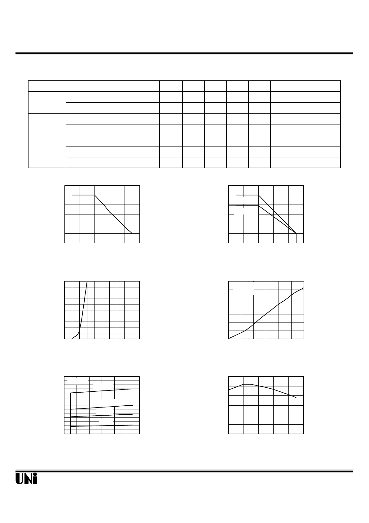
Typical Optical-Electrical Characteristic Curves
60
50
(mA)
F
40
30
20
10
Forward Current I
0
-25 0 25 50 75 100
Ambient Temperature T
Fig.1 forward Current VS
Ambient Temperature
100
(mA)
80
F
60
40
20
Forward Current I
0
0.8 1.2 1.6 2.0 2.4 2.8
Forward Voltage VF (V)
Fig.3 Forward Current VS
Forward Voltage
2.8
A)
µ
Collector Current Ic (
Ta=25℃
2.4
2.0
1.6
1.2
0.8
0.4
0.0
0 2 4 6 8 10 12
20mA
IF=15mA
Collector-Emitter Voltage Vce (V)
Fig.5 Collector Current vs. Vce
A
.
120
100
Power Dissipation (mW)
P
80
60
40
20
0
TOT
-25 0 25 50 75 100
Ambient Temperature TA ( oC )
Fig.2 Power Dissipation vs
2.8
Vce=2V
2.4
Ta=25℃
2.0
1.6
1.2
0.8
0.4
Collector Current Ic (mA)
0.0
0 5 10 15 20 25 30
Forward Current IF (mA)
Fig.4 Collector Current vs
Forward Current
120
100
80
60
40
20
0
Relative Collector Current (%)
-25 0 25 50 75 100
Ambient Temperature TA ( oC)
Fig.6 Relative Collector Current VS. T
IF =20mA
VR =5V
Ic=0.1mA,Ee=0.1mW/cm
IF =20mA, Vce =5V
RL =1k, d =1mm
A
2
Unity Opto Technology Co., Ltd.
04/01/2002
 Loading...