

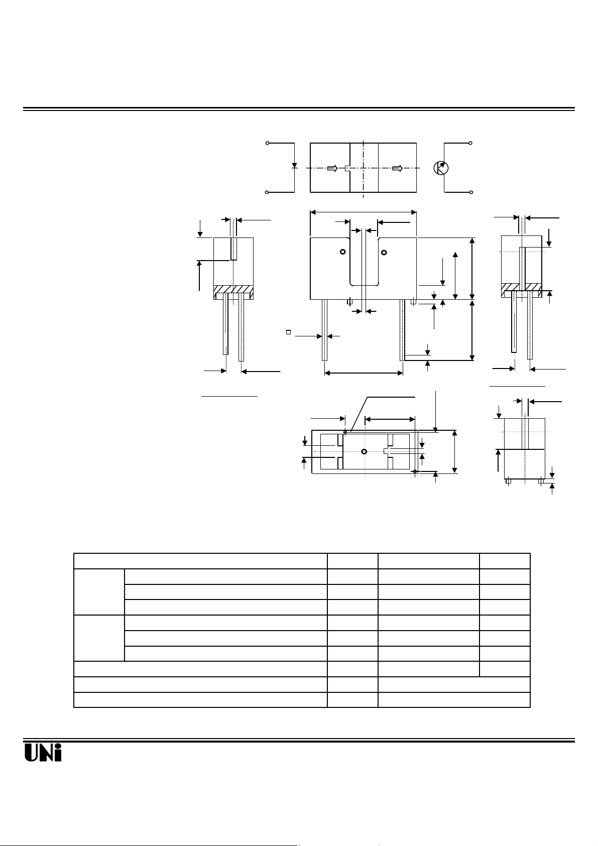
SLOTTED
PHOTOINTERRUPTER
MIT-5A116-U
(.406±.012)
5.20± 0.10
(.260±.004)
A'
(.020)
2.54 NOM
A-A' SECTION
B
B'
B-B' SECTION
(.100)
2
Description Package Dimensions
The MIT-5A116-U consists of a Gallium Arsenide
infrared emitting diode and a NPN silicon phototransistor built in a black plastic housing . It is a transmissive subminiature photointerrupter.
1
0.50 ± 0.10
(.020±.004)
14.00(.551)
5.00± 0.20
(.197±.008)
4
3
0.50± 0.10
(.020±.004)
Features
l Non -contact switching
l For- direct pc board
l Dual - in - line socket mounting
l Fast switching speed
l Choice of mounting configuration.
Absolute Maximum Ratings
Continuous Forward Current
INPUT Reverse Voltage
Power Dissipation
Collector-emitter breakdown voltage
OUTPUT Emitter-Collector breakdown voltage
Collector power dissipation
Total power dissipation
Operating Temperature Range
Storage Temperature Range
3.70± 0.20
(.146±.008)
(.100)
0.50TYP
1.70
(.067)
2.35 ± 0.10
(.038±.004)
9.00± 0.30
2-φ 0.70± 0.10
(.028±004)
6.60± 0.10
2.50(.098)
0.70(.028)
1.00(.040) MIN
0.90
(.035)
(.205±.004)
7.50 ± 0.30
6.00
(.295±.012)
10.00MIN
(.236)
10.00(.394)
(.394)
5.20(.205)
NOTE
1. Tolerance is ± 0.25 mm (.006") unless otherwise noted.
@TA =25oC
Parameter Symbol Maximum Rating Unit
V
P
V
(BR)CEO
V
(BR)ECO
P
T
T
I
P
TOT
opr
F
R
ad
C
stg
50 mA
5 V
75 mW
30 V
5 V
75 mW
100
o
C to + 85oC
o
C to + 100oC
mW
6.00 ± 0.10
1.50(.059)
(.236±.004)
0.70 (.027)
Unity Opto Technology Co., Ltd.
04/01/2002
MIT-5A116-U
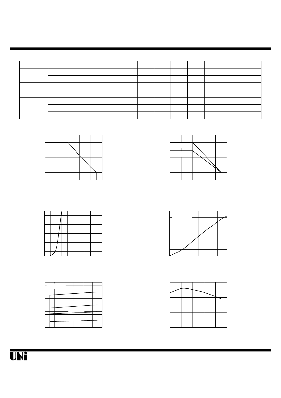
Optical-Electrical Characteristics
PD , P
C
A
Forward Current I
(mA)
Ta=25oC
4mA
Parameter symbol Min. Typ. Max. Unit. Test Conditions
Input Forward Voltage
Reverse Current
V
F
I
R
- 1.2 1.4 V
- - 10
µA
Output Collector Dark Current Iceo - - 100 nA Vce =10V
Collector Emitter Saturation Voltage
V
CE(SAT)
- - 0.4 V
Collector Current Ic (on) 0.4 - 4 mA
Transfer Cha- Response Time (RISE)
racteristics Response Time (FALL)
t
r
t
f
- 20 100
- 20 100
µS Ic=100µA, Vce =5V
µS
Typical Optical-Electrical Characteristic Curves
60
50
(mA)
F
40
30
20
10
Forward Current I
0
-25 0 25 50 75 100
Ambient Temperature T
Fig.1 forward Current VS
Ambient Temperature
A
.
120
100
80
60
40
20
Power Dissipation (mW)
P
TOT
0
-25 0 25 50 75 100
Ambient Temperature TA (oC )
Fig.2 Power Dissipation vs
Ambient Temperature
@TA =25oC
IF =20mA
VR =5V
Ic=0.1mA,Ee=0.1mW/cm
IF =20mA, Vce =5V
RL =1k, d =1mm
2
100
80
F
60
40
20
0
0.8 1.2 1.6 2.0 2.4 2.8
Forward Voltage VF (V)
Fig.3 Forward Current VS
Forward Voltage
700
A)
600
µ
500
400
300
200
100
Collector Current Ic (
0
0 2 4 6 8 10 12
20mA
IF=15mA
10mA
Collector-Emitter Voltage Vce (V)
Fig.5 Collector Current vs. Vce
700
A)
µ
Collector Current Ic (
Vce=2V
600
500
400
300
200
100
0
0 5 10 15 20 25 30
o
Forward Current IF (mA)
Fig.4 Collector Current vs
Forward Voltage
120
100
80
60
40
20
0
Relative Collector Current (%)
-25 0 25 50 75 100
Ambient Temperature TA ( oC )
Fig.6 Relative Collector Current VS. T
Unity Opto Technology Co., Ltd.
04/01/2002

MIT-5A116-U
Typical Optical-Electrical Characteristic Curves
tr
0
+
0
+
-6
10
CEO
Collector Dark Current I
10
10
10
10
VCE=20V
-7
-8
-9
-10
0 25 50 75 100
Ambient Temperature TA (o C )
Fig.7 Collector Dark Current vs.
Ambient Temperature
100
80
60
40
20
Relative Sensitivity (%)
0
700 800 900 1000 1100 1200
Wavelength (nm)
Fig.9 Spectral Sensitivity (Detecting side)
Ta=25 oC
1000
100
10
VCE=2V
IC=100mA
Ta=25oC
4
s)
µ
1
Response Time (
0.1
0.01 0.1 1 10 100
Load Resistance Rt (KΩ)
Fig.8 Response Time vs.
Load Resistance
Response Time Measurement Circuit
Input
90 %
Output
10 %
Input V
t
t
tf
IL
VR
Output
CC
Sensing Position Characteristics
(Typical)
IF=20mA
VCE=5V
(%)
L
100
o
50
Relative light current I
0
-2 -1 0 +1 +2 (mm) -2 -1 0 +1 +2 (mm)
Distance d (mm)
Unity Opto Technology Co., Ltd.
YX
IF=20mA
VCE=5V
o
(Center of optical axis)
X
Y
04/01/2002
 Loading...