

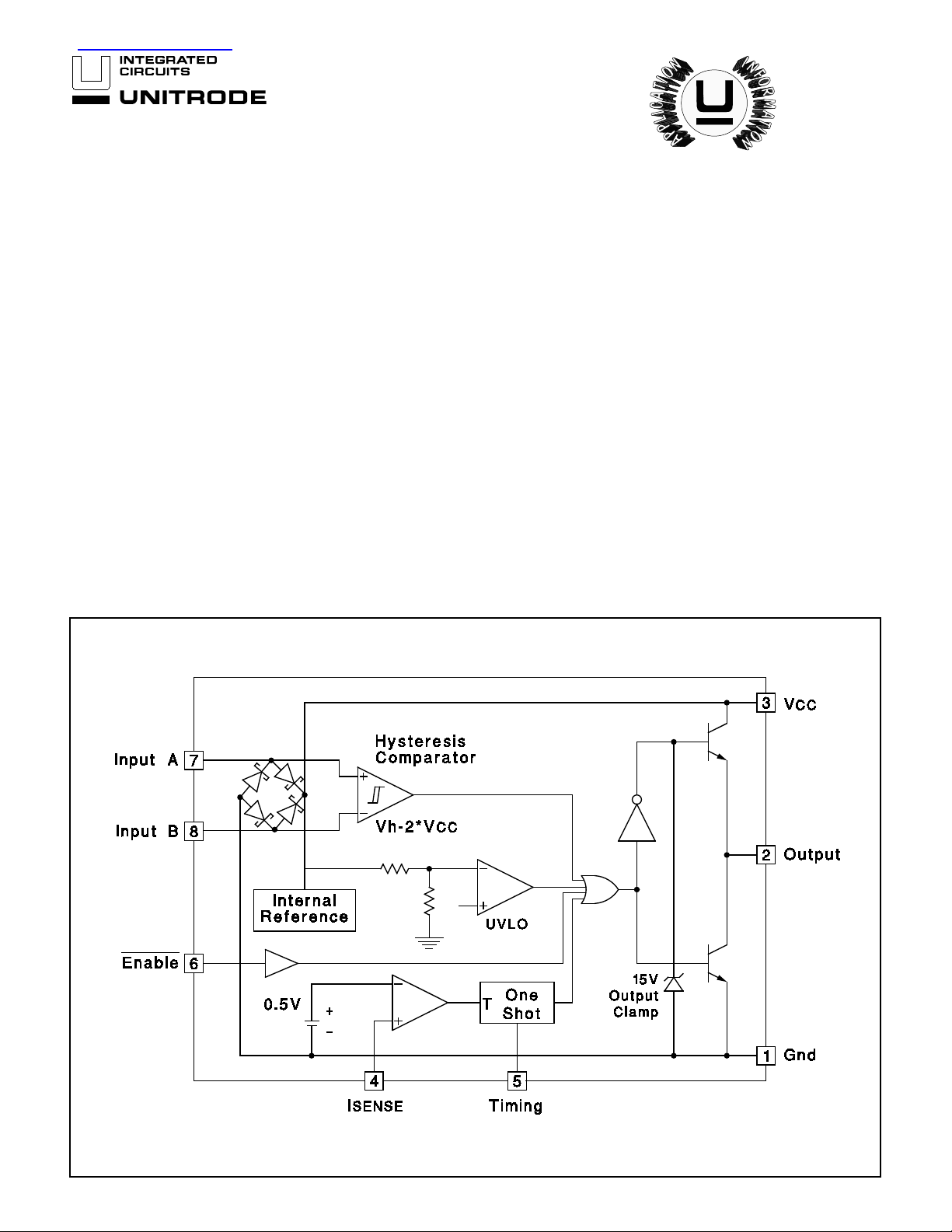
The UC1725 and its companion chip, the UC1724, provide all the necessary features to drive an isolated MOSFET transistor from a TTL input signal. A unique modulation scheme is used to transmit both power
and signals across an i solation boundary with a minimum of external
components.
Protection circui try, including under-voltage lockout, over-current shutdown, and gate voltage clamping provide fault protection for the MOSFET. High level gate drive is guaranteed to be greater than 9 volts and
less than 15 volts under all conditions.
Uses include isolated off-l ine full bri dge and half bridge drives for driving motors, switches, and any other load requi ring full el ectrical isolation.
The UC1725 is characterized for operation over the full military temperature range of -55°C to +125°C while the UC2725 and UC3725 are
characterized for -25°C to +85°C and 0°C to +70°C respectively.
查询UC1725供应商
Isolated High Side FET Driver
FEATURES DESCRIPTION
• Receives Both Power and Signal Across
the Isolation Boundary
• 9 to 15 Volt High Level Gate Drive
• Under-voltage Lockout
• Programmable Over-current Shutdown
and Restart
• Output Enable Function
UC1725
UC2725
UC3725
BLOCK DIAGRAM
1/94
UDG-92051-1
ABSOLUTE MAXIMUM RATINGS
(Unless otherwise st at ed, these specifications apply for -55°C≤TA≤+125°C fo r
UC1725; -25°C≤TA≤+85°C for UC2725; 0°C≤TA≤+70°C for UC3725; VCC (pin 3) =
0 to 15V, RT=10k, CT=2.2nf, T A =TJ, pin numbers refer to DIL-8 package. )
Supply Voltage (pin 3) . . . . . . . . . . . . . . . . . . . . . . . . . . . . . 30V
Power inputs (pins 7 & 8). . . . . . . . . . . . . . . . . . . . . . . . . . . 30V
Output curre nt , sourc e or sink (pin 2)
DC. . . . . . . . . . . . . . . . . . . . . . . . . . . . . . . . . . . . . . . . . . . . 0.5A
Pulse (0.5 us) . . . . . . . . . . . . . . . . . . . . . . . . . . . . . . . . . . . 2.0A
Enable and Current limit input s (pin s 4 & 6). . . . . . . . -0.3 to 6V
Power Dissipation at T
Power Dissipation at T
Lead Temperat ure (Solde ring, 10 Sec onds ) . . . . . . . . . . 300°C
Note 1: Unless otherwise indica te d, voltages ar e re feren ced t o
ground and curre nts are posit ive into , negat ive out of , the specified terminals (pin num ber s refer to DIL-8 pac kage ).
Note 2: See Unitrod e Inte gra ted C ircuit s datab ook f or
information regar ding t her m al specif icat ions an d limita tion s of
packages.
A ≤ 25°C (DIL-8). . . . . . . . . . . . . . . . 1W
A ≤ 25°C (SO-14 ) . . . . . . . . . . . . 725mW
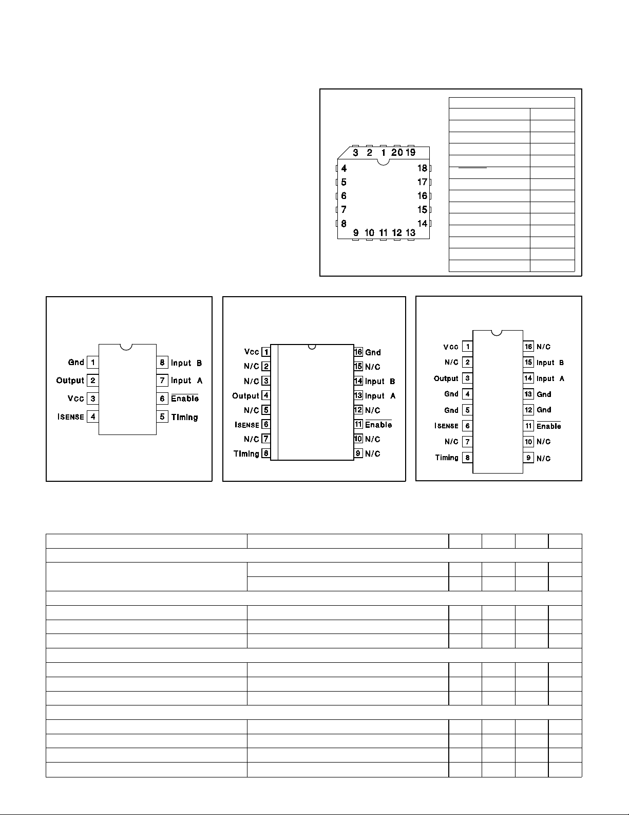
CONNECTION DIAGRAMS
PLCC-20 (Top View)
Q Package
UC1725
UC2725
UC3725
PACKAGE PIN FUNCTION
FUNCTION PIN
N/C 1
SENSE 2
I
N/C 3-5
Timing 6
Enable 7
N/C 8-9
Input A 11
N/C 12-14
Input B 15
Gnd 16
CC 17
V
N/C 18-19
Output 20
DIL-8 (Top View)
J Or N Package
SOIC-16 (Top View)
DW Package
ELECTRICAL CHARACTERISTICS:
PARAMETER TEST CONDITION S MIN TYP MAX UNITS
POWER INPUT SECTIO N (PINS 7 & 8)
Forward Diode Drop, Schottky Rect ifier I
CURRENT LIMIT SECTION (PIN 4)
Input bias current V
Threshold vo ltag e 0.4 0.5 0.6 V
Dela y to outp ut s V
TIMING SECTION (PIN 5)
Output Off Time 27 30 33 µs
Upper Mono Threshold 6.3 7.0 7.7 V
Lower Mono Threshold 1.9 2.0 2.3 V
HYSTERESIS AMPLIFIER (PINS 7 & 8)
Input Open Circu it Volt age Inputs (pins 7 & 8), Open C ircuited, T
Input Impedance T
Hystere s i s 26.5 2*Vcc 30.5 V
Dela y to Outp uts V
F = 50ma .55 .7 V
I
F = 500ma 1.1 1.5 V
PIN4 = OV -1 -10 µA
PIN4 = 0 to 1V 100 250 ns
A = 25°C 23 28 33 k Ω
PIN7 - VPIN8 = VCC + 1V 100 300 ns
2
DIL-16 (Top View)
JE Or NE Package
A= 25°C 7.0 Vcc/2 8.0 V
 Loading...