

查询UC3724N供应商
Isolated Drive Transmitter
UC1724
UC2724
UC3724
FEATURES
• 500mA Output Drive, Source or Sink
• 8 to 35V Operation
• Transmits Logic Signal Instantly
• Programmable Operating Frequency
• Under-Voltage Lockout
• Able To Pass DC Information Across
Transformer
• Up To 600kHz Operation
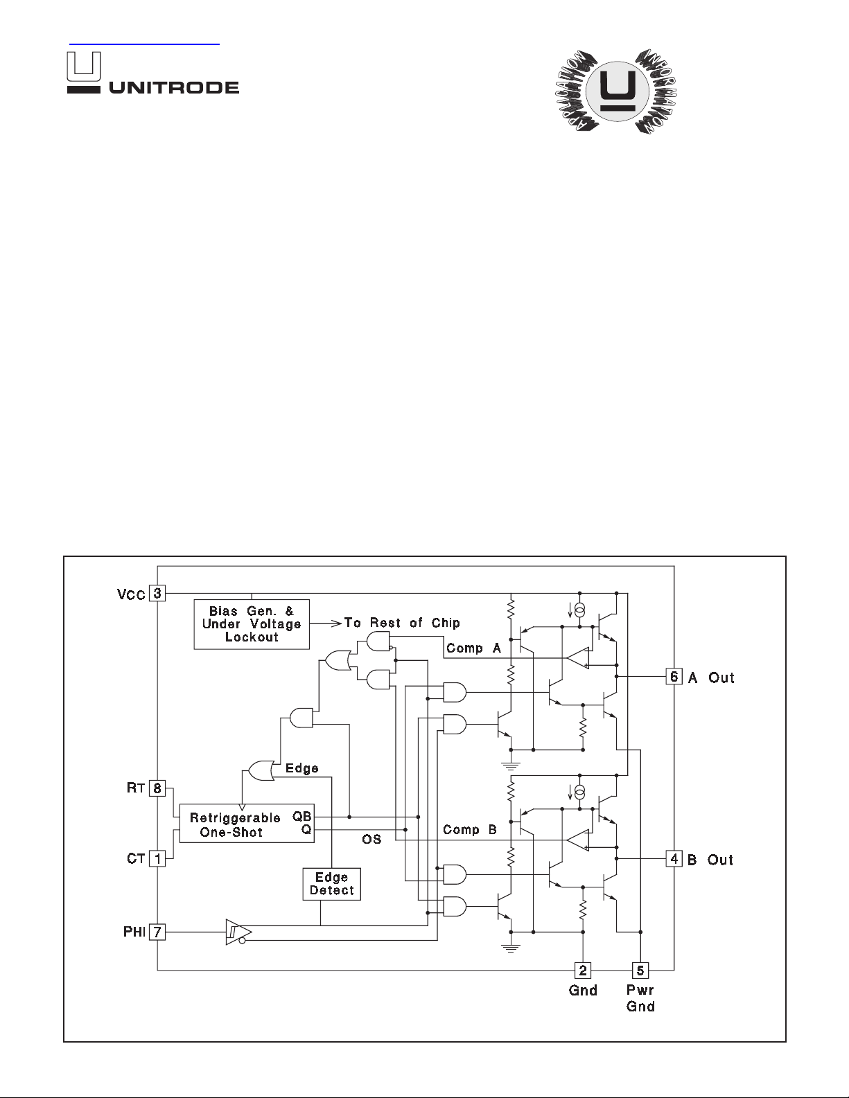
BLOCK DIAGRAM
DESCRIPTION
The UC1724 family of Isolated Drive Transmitters, along with the UC1725
Isolated Drivers, provide a unique solution to driving isolated power
MOSFET gates. They are particularly suited to drive the high-side devices
on a high-voltage H-bridge. The UC1724 devices transmit drive logic, and
drive power, to the isolated gate circuit using a low cost pulse transformer.
This drive system utilizes a duty-cycle modulation technique that gives instantaneous response to the drive control transistions, and reliably passes
steady-state, or DC, conditions. High frequency operation, up to 600kHz,
allows the cost and size of the coupling transformer to be minimized.
These devices will operate over an 8 to 35 Volt supply range.The dual high
current totem pole outputs are disabled by an uder-voltage lockout circuit to
prevent spurious responses during startup or low voltage conditions.
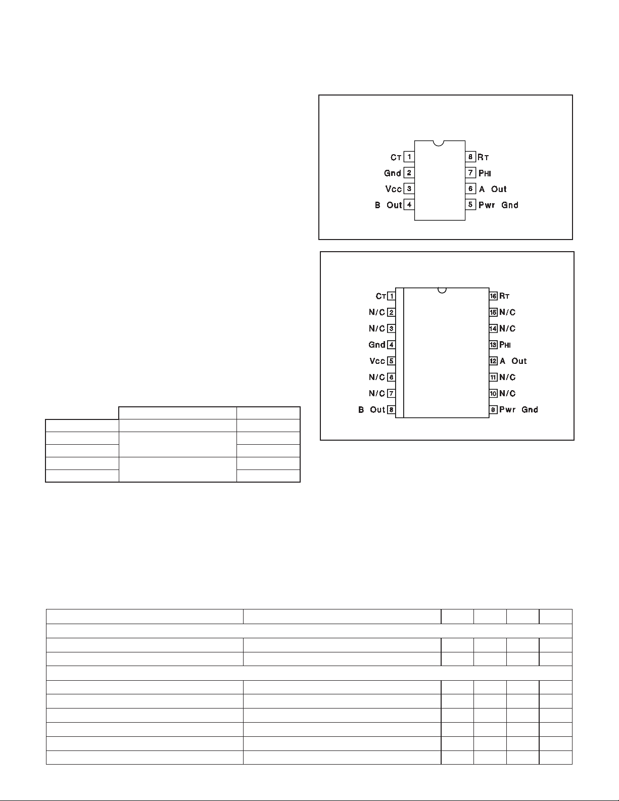
These devices are available in 8 pin plastic or ceramic dual-inline packages, as well as 16 pin SOIC package.
Note: Pin numbers refer to DIL-8 packages.
04/99
UDG-92037
ABSOLUTE MAXIMUM RATINGS
Supply Voltage VIN. . . . . . . . . . . . . . . . . . . . . . . . . . . . . . . 40V
Source/Sink Current (Pulsed) . . . . . . . . . . . . . . . . . . . . . . . . 1A
Source/Sink Current (Continuous) . . . . . . . . . . . . . . . . . . . 0.5A
+
Ouput Voltage (Pins 4, 6). . . . . . . . . . . . . . . –0.3 to (V
P
HI, RT, and CT inputs (Pins 1, 7, and 8) . . . . . . . . . –0.3 to 6V
Operating Junction Temperature (Note 2). . . . . . . . . . . .150°C
Storage Temperature Range . . . . . . . . . . . . . . –65°C to 150°C
Lead Temperature (Soldering, 10 Seconds) . . . . . . . . . . 300°C
0.3)V
IN
Note 1: All voltages are with respect to GND (Pin 2); all cur-
rents are positive into, negative out of part.
Note 2: Consult Unitrode Integrated Circuit Databook for ther-
mal limitations and considerations of package.
Note 3: Pin numbers refer to DIL-8 packages.
RECOMMENDED OPERATION CONDITIONS
Input Voltage . . . . . . . . . . . . . . . . . . . . . . . . . . . . . +9V to +35V
Sink/Source Load Current (each output). . . . . . . . . 0 to 500mA
Timing Resistor. . . . . . . . . . . . . . . . . . . . . . . . . . . 2kW to 10kW
Timing Capacitor . . . . . . . . . . . . . . . . . . . . . . . . . 300pF to 3nF
Operating Temperature Range (UC1724). . . –55°C<TA<125°C
Operating Temperature Range (UC3724). . . . . . 0°C<TA<70°C
Note 4: Range over which the device is functional and
parameter limits are guaranteed.
UC1724
UC2724
UC3724
CONNECTION DIAGRAMS
DIL-8 (Top View)
J Or N Package
SOIC-16 (Top View)
DW Package
ORDERING INFORMATION
TEMPERATURE RANGE PACKAGE
UC1724J –55°C to +125°C CDIP
UC2724DW –25°C to +85°C SOIC-Wide
UC2724N PDIP
UC3724DW 0°C to +70°C SOIC-Wide
UC3724N PDIP
ELECTRICAL CHARACTERISTICS: Unless otherwise stated, V
output and these specifications apply for: –55oC < TA< 125oC for the UC1724, –25oC < TA< 85oC for the UC2724, and
0oC < TA < 70oC for the UC3724. TA=TJ.
PARAMETER TEST CONDITIONS MIN TYP MAX UNITS
Under-Voltage Lockout
Start-Up Threshold V
Threshold Hysteresis 0.4 1.0 1.5 V
Retriggerable One-Shot
Initial Accuracy T
Temperature Stability Over Operating T
Voltage Stability V
Operating Frequency L
Minimum Pulse Width RT = 2k CT = 300pF 100 500 1200 ns
Operating Frequency RT = 2k C
Rising 7.75 9.5 V
IN
= 25°C 1.54 1.9 2.25 µs
J
J
= 10 to 35V 0.2 0.5 %/V
IN
= 1.4mH 100 150 200 kHz
LOAD
T = 300pF L
= 20V, RT= 4.3kΩ, CT= 1000pF, no load on any
CC
1.0 2.9 µs
= 1.4mH 500 750 1100 kHz
LOAD
2
 Loading...