

查询UC3717A供应商
Stepper Motor Drive Circuit
FEATURES DESCRIPTION
• Full-Step, Half-Step and Micro-Step
Capability
• Bipolar Output Current up to 1A
• Wide Range of Motor Supply Voltage
10-46V
• Low Saturation Voltage with Integrated
Bootstrap
• Built-In Fast Recovery Commutating
Diodes
• Current Levels Selected in Steps or Varied
Continuously
• Thermal Protection with Soft Intervention
ABSOLUTE MAXIMUM RATINGS (Note 1)
Voltage
Logic Supply, VCC. . . . . . . . . . . . . . . . . . . . . . . . . . . . . . . . . . . . . . 7V
Output Supply, Vm. . . . . . . . . . . . . . . . . . . . . . . . . . . . . . . . . . . . . 50V
Input Voltage
Logic Inputs (Pins 7, 8, 9) . . . . . . . . . . . . . . . . . . . . . . . . . . . . . . . . 6V
Analog Input (Pin 10). . . . . . . . . . . . . . . . . . . . . . . . . . . . . . . . . . . V
Reference Input (Pin 11) . . . . . . . . . . . . . . . . . . . . . . . . . . . . . . . . 15V
Input Current
Logic Inputs (Pins 7, 8, 9) . . . . . . . . . . . . . . . . . . . . . . . . . . . . . -10mA
Analog Inputs (Pins 10, 11). . . . . . . . . . . . . . . . . . . . . . . . . . . . -10mA
Output Current (Pins 1, 15) . . . . . . . . . . . . . . . . . . . . . . . . . . . . . . . ±1.2A
Junction Temperature, TJ. . . . . . . . . . . . . . . . . . . . . . . . . . . . . . . +150°C
Storage Temperature Range, TS. . . . . . . . . . . . . . . . . . -55°C to +150°C
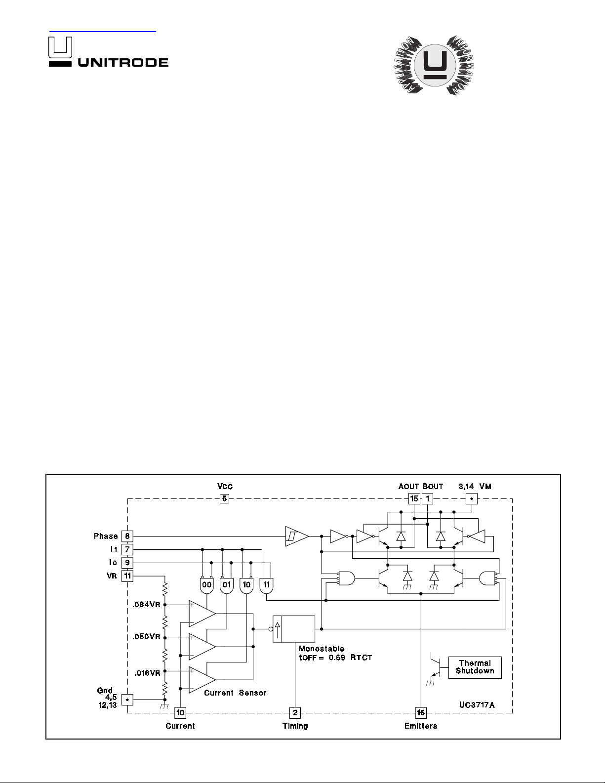
The UC3717A is an impro ved ver sion of the UC3717, us ed to switch
drive the current in one winding of a bipolar stepper motor. The
UC3717A has been modified to supply higher winding current, more
reliable thermal protection, and improved efficiency by providing integrated bootstrap circuitry to lower recirculation saturation voltages.
The diagram shown below presents the building blocks of the
UC3717A. Includ ed are an LS-TTL compatible l ogic input, a current
sensor, a monostable, a ther mal shutd ow n netw ork, and an H-bri dge
output stage. The output stage features built-in fast recovery commutating diodes and integrated bootstrap pull up. Two UC3717As
and a few external components form a complete control and drive
unit for LS-TTL or micro-processor controlled stepper motor systems.
The UC3717A is characterized for operation over the temperature
range of 0°C to +70°C.
CC
UC3717A
Note 1: All voltages are with respect to ground, Pins 4,
5, 12, 13. Currents are positive into, negative out of the
specified terminal. Pin numbers refer to DIL-16 package.
Consult Packaging Section of Databook for thermal limitations and considerations of package.
BLOCK DIAGRAM
4/97
1
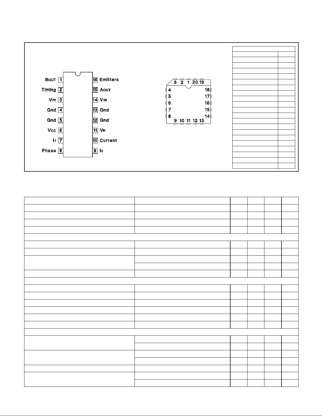
CONNECTION DIAGRAMS
UC3717A
DIL-16 (TOP VIEW)
J or N Package
ELECTRICAL CHARACTERISTICS
PLCC-20 (TOP VIEW)
Q Package
(Refer to the te st c irc ui t, F ig ure 6 . Vm = 36V, VCC = 5V, VR = 5V, TA = 0°C to 70°C,
PACKAGE PIN FUNCTION
FUNCTION PIN
N/C
B
OUT
Timing
m
V
Gnd
N/C
Gnd
V
CC
I
1
Phase
N/C
I
0
Current
V
R
Gnd
N/C
Gnd
m
V
A
OUT
Emitters
unless otherwis e stat ed , TA = TJ.)
PARAMETERS TEST CONDITIONS MIN TYP MAX UNITS
Supply Voltage, Vm (Pins 3, 14) 10 46 V
Logic Supply Voltage, V
Logic Supply Current, I
(Pin 6) 4.75 5.25 V
CC
(Pin 6) IO = I1 = 0 7 15 mA
CC
Thermal Shutdown Temperature +160 +180 °C
Logic Inputs
Input Low Voltage, (Pins 7, 8, 9) 0.8 V
Input High Voltage, (Pins 7, 8, 9) 2 V
Low Voltage Input Current, (Pins 7, 8, 9) V
High Voltage Input Current, (Pins 7, 8, 9) V
= 0.4V, Pin 8 -100
I
V
= 0.4V, Pins 7 and 9 -400 mA
I
= 2.4V 10
I
CC
Comparators
Comparator Low, Thres ho ld Volt ag e (Pin 10) V
Comparator Medium, Threshold Voltage (Pin 10) V
Comparator High, Thre sh ol d Vol tage (Pin 10) V
Comparator Input, Current (Pin 10)
Cutoff Time, t
Turn Off Dela y, t
OFF
D
= 5V; IO = L; I1 = H 668090mV
R
= 5V; IO = H; I1 = L 236 250 266 mV
R
= 5V; IO = L; I1 = L 396 420 436 mV
R
20
±
RT = 56kΩ, CT = 820pF 25 35
(See Figure 5) 2
Source Diode-Transistor Pair
Saturation Voltage, V
(See Figure 5) I
Saturation Voltage, V
(See Figure 5) I
Leakage Current V
Diode Forward Voltage, V
(Pins 1, 15) Im = -0.5A, Conduction Period 1.7 2.1 V
SAT
= -0.5A, Recirculation Period 1.1 1.35 V
m
(Pins 1, 15) Im = -1A, Conduction Period 2.1 2.8 V
SAT
= -1A, Recirculation Period 1.7 2.5 V
m
= 40V 300
m
F
Im = -0.5A 1 1.25 V
I
= -1A 1.3 1.7 V
m
10
11
12
13
14
15
16
17
18
19
20
1
2
3
4
5
6
7
8
9
V
A
µ
A
µ
A
µ
s
µ
s
µ
A
µ
2
UC3717A
ELECTRICAL
CHARACTERISTICS (cont.)
PARAMETERS TEST CONDITIONS MIN TYP MAX UNITS
Sink Diode-Transistor Pair
Saturation Voltage, V
Leakage Current V
Diode Forward Voltage, V
(Pins 1, 15) Im = 0.5A 0.8 1.1 1.35 V
SAT
F
(Refer to the te st c irc ui t, F ig ure 6 . VM = 36V, VCC = 5V, VR = 5V, TA = 0°C to 70°C, unless
otherwise stated, TA = TJ.)
I
= 1A 1.6 2.3 V
m
= 40V 300
m
Im = 0.5A 1.1 1.5 V
= 1A 1.4 2 V
I
m
µ
A
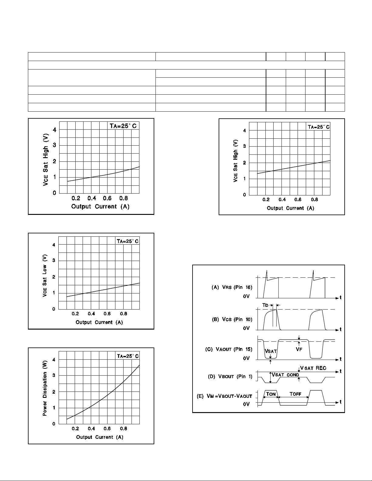
Figure 1. Typical Source Saturation Voltage
vs Output Current (Recirculation Period)
Figure 3. Typical Sink Saturation
Voltage vs Output Current
Figure 2. Typical Source Saturation Voltage
vs Output Current (Conduction Period)
Figure 4. Typical Power Dissipation
vs Output Current
Figure 5. Typical Waveforms with MA Regulating
(phase = 0)
3
 Loading...