

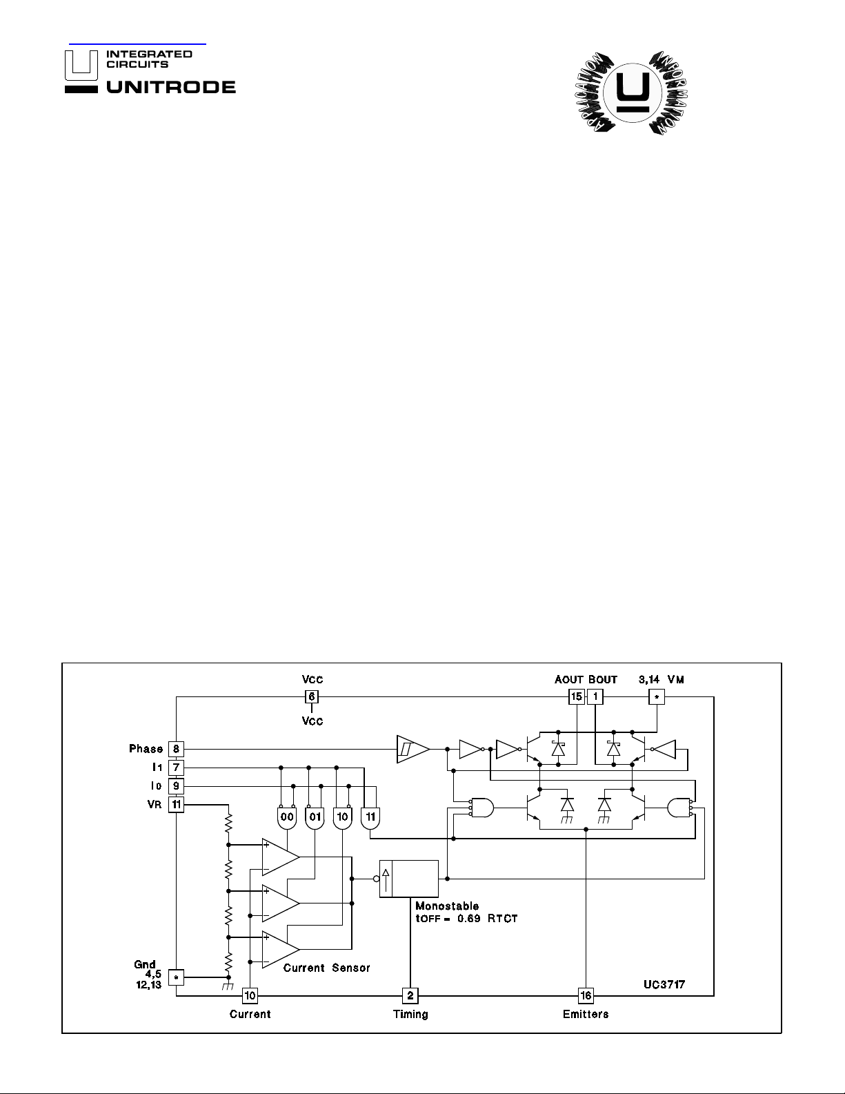
The UC3717 has been designed to control and drive the current in
one winding of a bipolar stepper motor . The circuit consists of an LSTTL-compatible logic input, a current senso r, a monostable and an
output stage with built-in protection diodes. Two UC3717s and a few
external components form a complete control and drive unit for LSTTL or micro-proces sor contr o lled stepper motor system s.
The UC1717 is characterized for operation over the full military temperature range of -55°C to +125°C, the UC2717 is characterized for
-25°C to +85°C, and the UC3717 is characterized for 0°C to +70°C.
查询UC1717供应商
Stepper Motor Drive Circuit
FEATURES DESCRIPTION
• Half-step and Full-step Capability
• Bipolar Constant Current Motor Drive
• Built-in Fast Recovery Schottky
Commutating Diodes
• Wide Range of Current Control 5-1000mA
• Wide Voltage Range 10-45V
• Designed for Unregulated Motor Supply
Voltage
• Current Levels can be Selected in Steps
or Varied Continuously
• Thermal Overload Protectio n
ABSOLUTE MAXIMUM RATINGS (Not e 1)
Voltage
Logic Supply, V
Output Supply, V
Input Voltage
Logic Inputs (Pins 7, 8, 9). . . . . . . . . . . . . . . . . . . . . . . . . . . . . . . . . . 6V
Analog Input (Pin 10) . . . . . . . . . . . . . . . . . . . . . . . . . . . . . . . . . . . . Vcc
Reference I nput (Pin 11) . . . . . . . . . . . . . . . . . . . . . . . . . . . . . . . . . 15V
Input Current
Logic Inputs (Pins 7, 8, 9) . . . . . . . . . . . . . . . . . . . . . . . . . . . . . . . -10mA
Analog Inputs (Pins 10, 11). . . . . . . . . . . . . . . . . . . . . . . . . . . . . . -10mA
Output Current (Pins 1, 15) . . . . . . . . . . . . . . . . . . . . . . . . . . . . . . . . ±1A
Junction Temperature, T
Storage Temperature Range, T
CC . . . . . . . . . . . . . . . . . . . . . . . . . . . . . . . . . . . . . . . 7V
M . . . . . . . . . . . . . . . . . . . . . . . . . . . . . . . . . . . . . . 45V
J. . . . . . . . . . . . . . . . . . . . . . . . . . . . . . . +150°C
S . . . . . . . . . . . . . . . . . . -55°C to +150°C
UC1717
UC2717
UC3717
Note 1: All voltages are with respect to ground, Pins
4,5, 12, 13. Pin num ber s refe r to DIL-16 packa ge. Currents are positive int o, negat ive ou t of the spe cified terminal.
Note 2: Consult Packaging Sect ion of Databook for information on thermal l imitat ions and considerations of
package.
BLOCK DIAGRAM
7/95
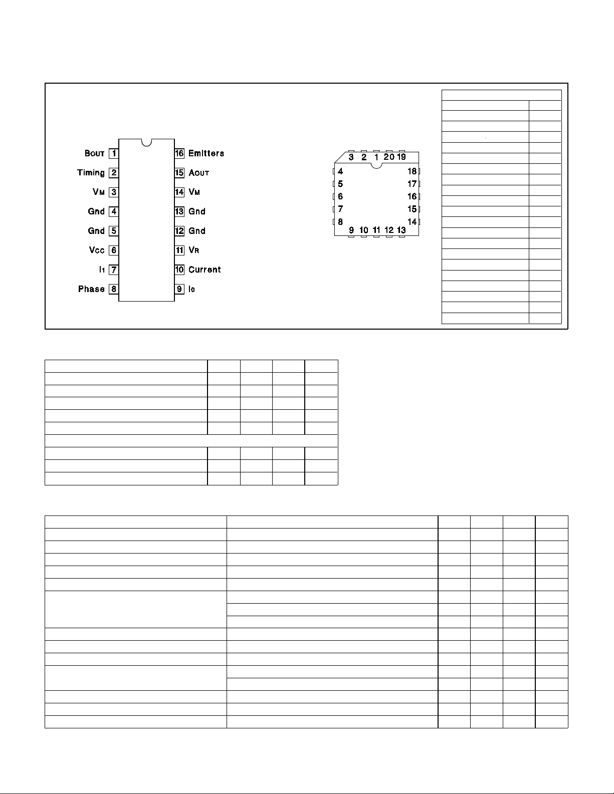
CONNECTION DIAG RAMS
Unless otherwise specified, these specifications apply for VCC = 5V, TA = TJ .
UC1717
UC2717
UC3717
DIL-16 (TOP VI EW)
J or N Package
RECOMMENDED OPERATING CONDITIONS
PARAMETER MIN TYP MAX UNITS
Supply Voltage, V
Supply Voltage, V
Output Current. I
Rise Time Logic Inputs, t
Fall Time Logic Inputs, t
Ambient Temperature, T
UC1717 -55 125 °C
UC2717 -25 85 °C
UC3717 0 70 °C
CC 4.75 5 5.25 V
M 10 40 V
M 20 800 mA
R 2 µs
F 2 µs
A
PLCC-20 (TOP VIEW)
Q Package
PACKAGE PIN FUNCTION
FUNCTION PIN
N/C
BOUT 2
Timing 3
VM 4
Gnd 5
N/C 6
Gnd 7
VCC 8
I1 9
Phase 10
N/C 11
I0 12
Current 13
VR 14
Gnd 15
N/C 16
Gnd 17
Vm 18
AOUT 19
Emitters 20
1
ELECTRICAL CHARACTERIST ICS
PARAMETER TEST CONDITIONS MIN TYP MAX UNITS
Supply Curren t, I
High-Level Input Voltage, Pins 7, 8, 9 2.0 V
Low-Level I nput Voltage, Pins 7, 8, 9 0.8 V
High-Level Input Current , Pins 7, 8, 9 V
Low Level Input Curre nt, Pins 7, 8, 9 V
Compara tor Thresh old Volta ge I
Compara to r Input Cur ren t -20 20 µA
Output Leakage Current I
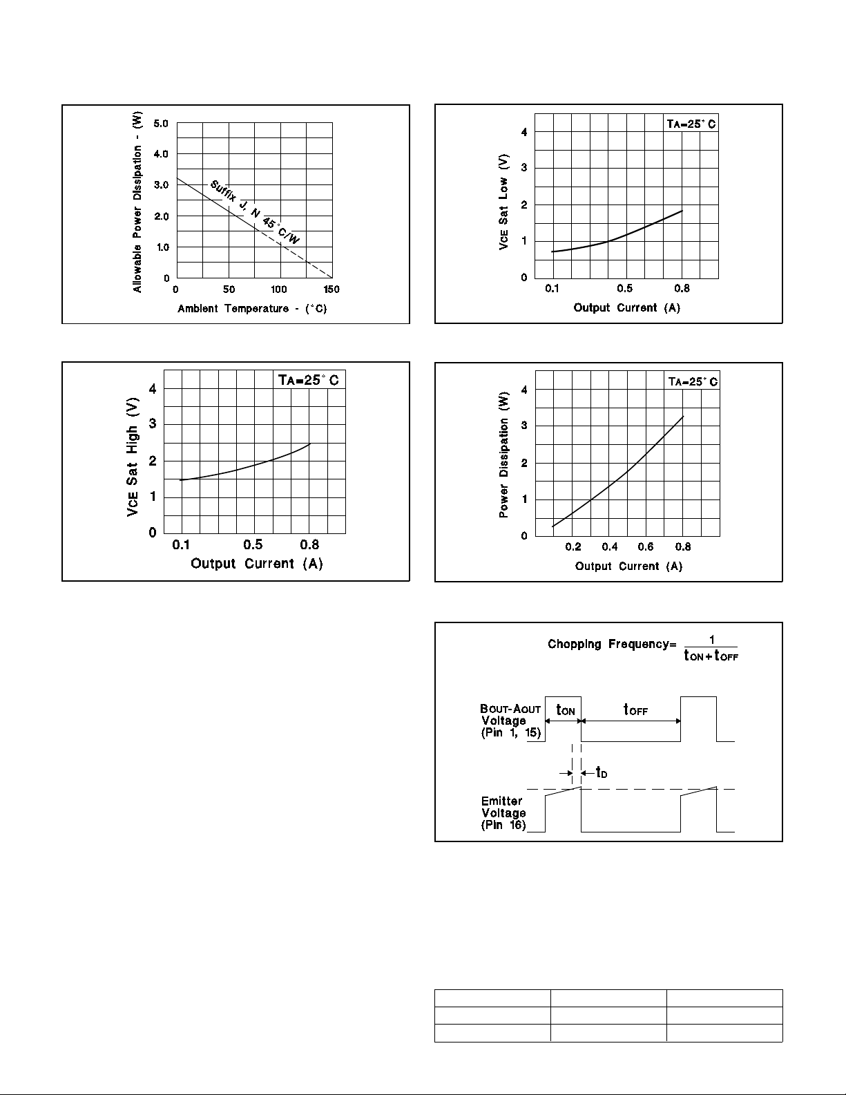
Total Saturation Voltage Drop I
Total Power Dissipation I
Cut Off Time, t
Turn Off Delay, t
Thermal Shutd own Jun ctio n Tem per atur e +160 +180 ° C
CC 25 mA
I = 2.4V 20 µA
I = 0.4V -0.4 mA
O = 0, I1 = 0, VR = 5.0V 390 420 440 mV
I
O = 1, I1 = 0, VR = 5.0V 230 250 270 mV
I
O = 0, I1 = 1, VR = 5.0V 65 80 90 mV
O = 1, I1 = 1, TA = +25°C 100 µA
M = 500mA 4.0 V
M = 500mA, fS = 30kHz 1.4 2.1 W
I
M = 800mA, fS = 30kHz 2.9 3.1 W
OFF VM = 10 V, tON≥ 5µs (See Figure 5 and 6) 25 30 35 µs
D TA = +25°C; dVc/dt ≥ 50mV/µs (See Figure 5 and 6) 1.6 2 .0 µs
2
UC1717
UC2717
UC3717
Figure 1
Figure 2: Ty pical Sour ce Satur at ion Voltage vs Outp ut Curr ent
FUNCTIONAL DESCRI PT IO N
The UC3717 drive circuit shown in the block diagram includes the following functions:
(1) Phase Logic and H-Bridge Output Stage
(2) V o ltag e D i v id er w i t h t h r e e C o m p a r a t ors f o r cur r e n t cont r o l
(3) Tw o Logic inputs for Digit al current lev el selec t
(4) Monostable for off time ge nerat ion
Figure 3: Ty pical Sink Sat ura tion Voltage vs Outpu t Cur rent
Figure 4: Typical Power Losse s vs Output Cur ren t
Input Logic: If any of the logic inputs are left open, the
circuit will treat it as a high level input.
Phase Input: The phase input terminal, pin 18, controls
the direction of the current through the motor winding.
The Schmidt-Trigger input coupled with a fixed time delay assures noise immunity and eliminates cross conduction in the output stage during phase changes. A low
level on the phase input will turn Q2 on and enable Q3
while a high level wi ll turn Q1 on and enable Q4. (See
Figure 7).
Output Stage: The output stage consists of four Darlington transistors and associated diodes connected in
an H-Bridge configuration. The diodes are needed to provide a current path when the transistors are being
switched. For fast recovery, Schottky diodes are used
Figure 5: Connections and Compone nt Values as in Figure 6.
across the source transistors. The Schottky diodes allow
the current to circulate through the winding while the sink
transistors are being switched off. The diodes across the
sink transistors in conjuncti on with the Schottkys provide
the path for the decaying current during phase reversal.
(See Figure 7).
PHASE INPUT Q1, Q4 Q2, Q3
Low Off On
High On Off
3
 Loading...