

Page 1
现货库存、技术资料、百科信息、热点资讯,精彩尽在鼎好!
UNISONIC TECHNOLOGIES CO., LTD
TL494
LINEAR INTEGRATED CIRCUIT
VOLTAGE MODE PWM
CONTROL CIRCUIT
DESCRIPTION
The UTC TL494 incorporates all the functions required in the
construction of a pulse-width modulation switching circuit.
Designed primarily for switching power supply control or DC-DC
convectors, it offers the systems engineer the flexibility to tailor
control circuitry to its own application.
FEATURES
*Complete PWM power control circuitry
*Uncommitted outputs for 200mA sink or source current
*Output control selects single ended or push pull operation
*Internal circuitry prohibits double pulses over total range
*Easy synchronization
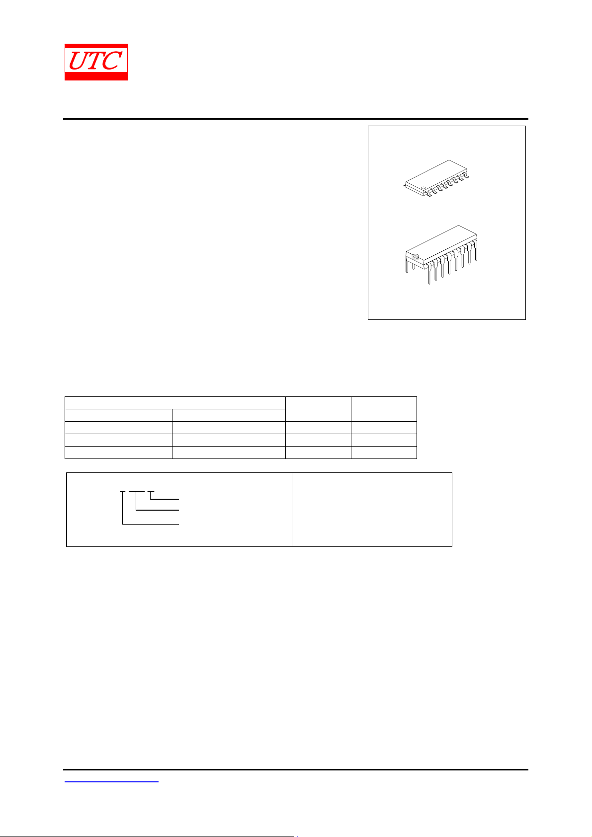
ORDERING INFORMATION
SOP-16
DIP-16
*Pb-free plating product number: TL494L
Order Number
Normal Lead Free Plating
TL494-D16-T TL494L-D16-T DIP-16 Tube
TL494-S16-R TL494L-S16-R SOP-16 Tape Reel
TL494-S16-T TL494L-S16-T SOP-16 Tube
TL494L-D16-T
(1)Packing Type
(2)Package Type
(3)Lead Plating
Package Packing
(1) R: Tape Reel, T: Tube
(2) D16: DIP-16, S16: SOP-16
(3) L: Lead Free Plating, Blank: Pb/Sn
www.unisonic.com.tw 1 of 7
Copyright © 2005 Unisonic Technologies Co., Ltd QW-R103-004,D
Page 2
TL494 LINEAR INTEGRATED CIRCUIT
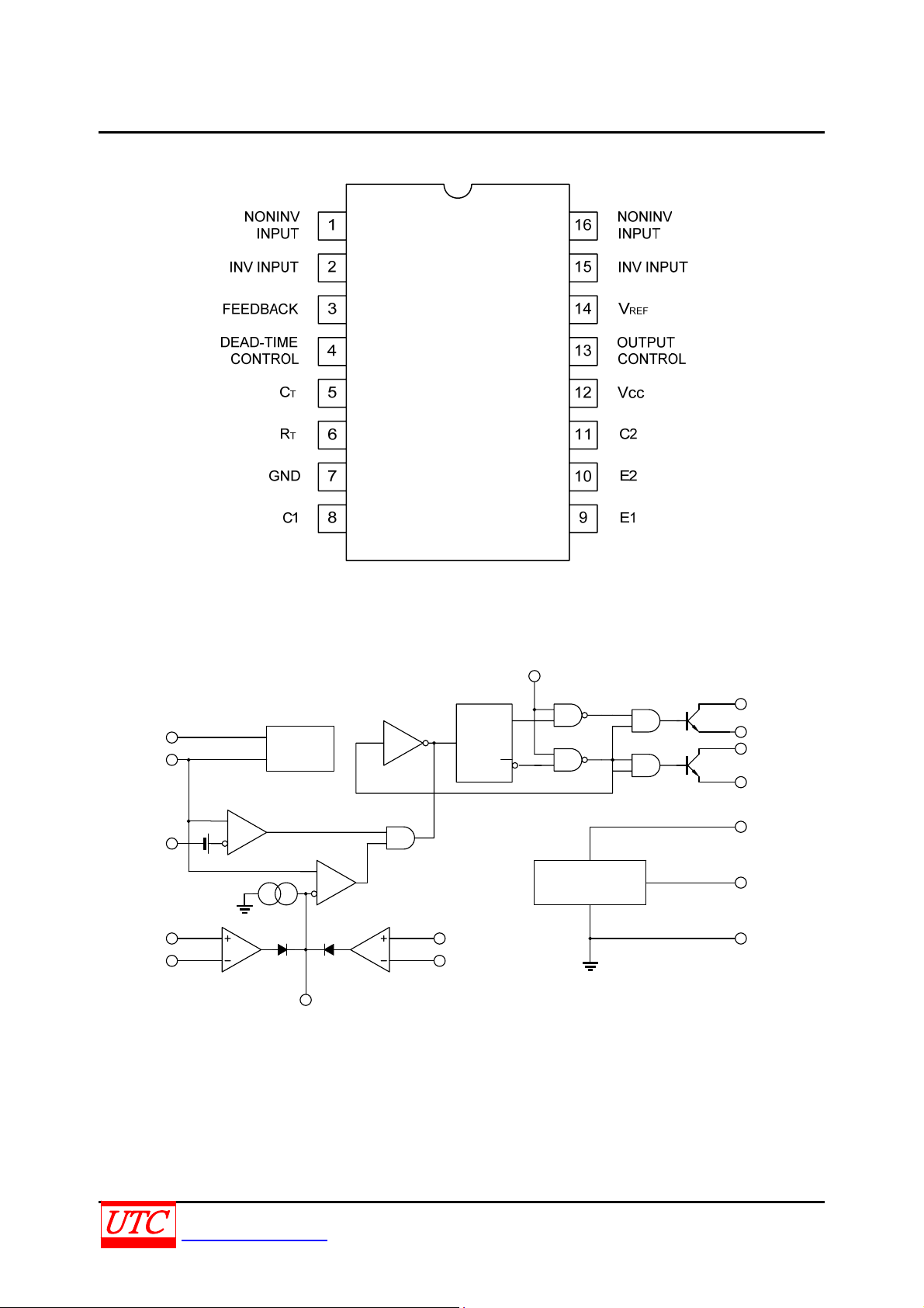
PIN CONFIGURATIONS
BLOCK DIAGRAM
RT
6
CT
5
dead time comparator
4
dead time
control
0.7mA
1
2
Error
Amplifier
oscillator
Pulse Steering
Flip-Flop
PWM comparator
Error
Amplifier
16
15
13
Input
control
C1
8
Q
T
Q
5V reference
regulation
Q1
Q2
V
Vcc
GND
REF
11
10
14
12
E1
9
C2
E2
7
UNISONIC TECHNOLOGIES CO., LTD 2 of 7
www.unisonic.com.tw QW-R103-004,D
Page 3
TL494 LINEAR INTEGRATED CIRCUIT
ABSOLUTE MAXIMUM RATINGS
(Unless otherwise noted all is over operating free air temperature range)
PARAMETER SYMBOL RATINGS UNIT
Supply Voltage(Note 3) VCC 41 V
Amplifier Input Voltage VIN V
Collector Output Voltage V
Collector Output Current ICO 250 mA
Continuous Total Dissipation
Junction Temperature TJ 125 °C
Operating Temperature T
Storage Temperature T
Note 1. Absolute maximum ratings are those values beyond which the device could be permanently damaged.
Absolute maximum ratings are stress ratings only and functional device operation is not implied.
2. All voltage values, except differential voltages are with respect to the network ground terminal.
Ta=25°C 1000 mW
Derate at Ta>25°C
41 V
OUT
PD
-25 ~ +85 °C
OPR
-40 ~ +150 °C
STG
RECOMMENDED OPERATING CONDITIONS
+0.3 V
CC
9.2 mW/°C
PARAMETER SYMBOL
Supply Voltage VCC 7 40 V
Amplifier Input Voltage VIN -0.3 Vcc-2 V
Collector Output Voltage V
Collector Output Current(each Transistor) Ic 200 mA
Current into Feedback If 0.3 mA
Timing Capacitor CT 0.47 10000 nF
Timing Resistor RT 1.8 500 kΩ
Oscillator Frequency fosc 1 300 kHz
Operating Free-Air Temperature Ta 0 70 °C
40 V
OUT
RATINGS
MIN MAX
UNIT
UNISONIC TECHNOLOGIES CO., LTD 3 of 7
www.unisonic.com.tw QW-R103-004,D
Page 4

TL494 LINEAR INTEGRATED CIRCUIT
ELECTRICAL CHARACTERISTICS
(Over recommended operating free-air temperature range, VCC=15V,f=1kHz,Unless otherwise specified)
PARAMETER SYMBOL TEST CONDITIONS MIN TYP MAX UNIT
Reference Section
Output Voltage V
Input Regulation VIN VCC=7V ~ 40V 2 25 mV
Output Regulation V
Output Voltage Change with Temperature
Short-Circuit Output Current I
Oscillator Section
Frequency F
Standard Deviation of Frequency
Frequency Change with Voltage
Frequency Change with Temperature
Amplifier Section
Input Offset Voltage Error V
Input Offset Current I
Input Bias Current I
Common-Mode Input Voltage Range Error VCC=7V ~ 40 V
Open-Loop Voltage Amplification
Unity-Gain Bandwidth GBW 800 kHz
Common-Mode Rejection Ratio Error CMRR
Output Sink Current(pin 3) I
Output source Current(pin 3) I
Output Section
Collector off-state current I
Emitter off-state Current I
Common-emitter VE=0, IC=200mA 1.1 1.3 V Collector -emitter
Saturation Voltage
Emitter-Follower V
Output Control Input Current VIN=V
Dead Time Control Section
Input bias (pin 4) I
Maximum duty cycle, each output VIN(pin 40=0 45 %
Input threshold Voltage(pin 4) V
Maximum duty cycle 0
PWM comparator Section
Input Threshold Voltage(pin 3) V
Input Sink Current (pin 3) I
Total Device
Standby Supply Current
VCC =15V
=40V
V
CC
Average supply current Vpin 4=2V 7.5 mA
Switching Characteristics, Ta=25°C
Output Voltage Rise Time tR 100 200 ns
Output Voltage Fall Time tF
Output Voltage Rise Time tR 100 200 ns
Output Voltage Fall Time tF
Note 1:All typical Values except for temperature coefficient are at Ta=25°C.
Note 2:For conditions shown as MIN or MAX, use appropriate value under recommended operating conditions.
Note 3:Duration of the short-circuit should not exceed one second.
Note 4:Standard deviation is a measure of the statistical distribution the mean as derived from the formula:
I
OUT
OUT
O(SC)
I(OFF)VOUT
I(OFF)
I(BIAS)
O(SINK)
O(SOURCE)VID
C(OFF)
E(OFF)
=1mA 4.75 5 5.25 V
OUT
I
=1 ~ 10mA 1 15 mV
OUT
ΔTa=MIN ~ MAX(note 2)
V
=0 35 mA
REF
=0.01μF, RT=120kΩ
C
T
All Values of VCC CT, RT, TA
constant
=7v ~ 40V,Ta=25°C
V
CC
=0.01μF, RT=12kΩ, ΔTa=MIN
C
T
~ MAX
0.2 1 %
10 kHz
10 %
0.1 %
12 %
(pin 3)=2.5V 2 10 mV
V
(pin 3)=2.5V 25 250 nA
OUT
V
(pin 3)=2.5V
OUT
=3V, V
ΔV
OUT
=40V,TA=25°C
V
CC
VID=-15mV ~ -5V
=0.5V ~ 3.5V
OUT
0.2 1
-0.3 ~
Vcc-2
70 95 dB
65 80 dB
0.3 0.7 mA
V(pin 3)=0.5V
=15mV ~ -5V, V(pin 3)=3.5V -2 mA
VCE=40V, VCC=40V
VCC=VC=40V, VE=0
=15V, IE=-200mA 1.5 2.5
C
3.5 mA
REF
2 100
-100
VIN=0 ~ 5.25V
I(BIAS)
Zero duty Cycle 3 3.3 V
THR
Zero Duty cycle 4 4.5 V
THR
Vpin 3= 0.7V 0.3 0.7 mA
I(SINK)
I
ST-BY
pin 6 at V
outputs open
, all other Inputs and
REF
Common-emitter configuration
Emitter-follower configuration
-2 -10
6 10 mA
9 15
25 100 ns
40 100 ns
μA
V
μA
μA
μA
UNISONIC TECHNOLOGIES CO., LTD 4 of 7
www.unisonic.com.tw QW-R103-004,D
Page 5

TL494 LINEAR INTEGRATED CIRCUIT
TEST CIRCUIT
Vcc=15V
VOLTAGE at C1
VOLTAGE at C2
TEST
INPUTS
50k
12k
0.01 F
4
DEAD-TIME
3
FEEDBACK
6
RT
5
CT
1
2
ERROR AMPLIFIER
16
15
13
OUTPUT CONTROL
12
Vcc
GND
7
2W 150 2W 150
REF OUTPUT
V
C1
E1
C2
E2
8
9
11
10
14
OUTPUT 1
OUTPUT 2
VOLTAGE at CT
DEAD-TIME
CONTROL INPUT
FEEDBACK
THRESHOLD VOLTAGE
THRESHOLD VOLTAGE
FIG 1. OPERATIONAL TEST CIRCUIT AND WAVEFORMS
UNISONIC TECHNOLOGIES CO., LTD 5 of 7
www.unisonic.com.tw QW-R103-004,D
Page 6

TL494 LINEAR INTEGRATED CIRCUIT
TEST CIRCUIT(Cont.)
ERROR
1
AMPLIFIER
Vin
2
16
Vref
15
AMPLIFIER
FIG 2. AMPLIFIER CHARACTERISTICS
FEEDBACK
TERMINAL
ERROR
UNISONIC TECHNOLOGIES CO., LTD 6 of 7
www.unisonic.com.tw QW-R103-004,D
Page 7

TL494 LINEAR INTEGRATED CIRCUIT
TYPICAL PERFORMANCE CHARACTERISTICS
UTC assumes no responsibility for equipment failures that result from using products at v alues that
exceed, even momentarily, rated values (such as maximum ratings, operating condition ranges, or
other paramet ers) listed i n products specif icat ions of any and al l UTC pr oducts described or contai ned
herein. UTC products are not designed f or use in life support appliances, dev ices or systems where
malf uncti on of t hese products can be reasonably expected t o result in personal inj ury. Reproduct ion in
whole or in part is prohi bited without t he prior written consent of the copyri ght owner. The inf ormati on
presented in thi s document does not form part of any quot ation or contract, is bel iev ed to be accurat e
and reliabl e and may be changed without notice.
UNISONIC TECHNOLOGIES CO., LTD 7 of 7
www.unisonic.com.tw QW-R103-004,D
 Loading...