


Table of Contents
1. Introduction....................................................................... 4
Overview..................................................................... 4
Icons........................................................................... 5
Hardware Specifications/Features................................. 6
Software Specifications.................................................8
Technical Support......................................................... 8
Returning Merchandise for Service................................ 9
2. Board Installation.............................................................. 10
Unpacking.................................................................... 10
Installation.................................................................... 11
Setting Jumpers............................................................ 11
3. Onboard Resource Settings.............................................. 12
Quick Reference for Jumpers........................................12
Map of Motherboard Jumpers....................................... 13
Soft Power Connector...................................................16
Sleep Button Connector.................................................16
Speaker Connector Installation...................................... 17
Hardware Reset Switch Connector Installation............... 17
CMOS RTC................................................................. 17
Flash EEPROM........................................................... 18
Hardware CMOS & Password Reset............................ 18
DRAM Installation....................................................... 18
Installing the CPU........................................................ 20
Peripheral Device Installation........................................ 25
Connecting the Power Supply........................................ 25
Frequently Asked Questions.......................................... 27
4. BIOS Configuration........................................................... 30
Standard Setup............................................................. 30
BIOS Features Setup.................................................... 32
Advanced Setup........................................................... 33
Chipset Setup............................................................... 38
Power Management Setup............................................ 47
PCI/PnP Setup............................................................. 50
Peripheral Setup........................................................... 53
Flash Writer Utility........................................................ 56

5. System Resources............................................................. 58
POST Checkpoint Codes.............................................. 58
Beep Codes................................................................. 66
Troubleshooting System Problems.................................. 67
Displayed Error Messages............................................ 68

Chapter 1
chapter 1
Introduction
Overview
The S1692S Tiger and S1692D Tiger 2 ATX are quality, high performance motherboards designed for Intel’s Pentium II microprocessors.
These motherboards utilize Intel’s 440LX AGP series chipset (also
called AGPset) and support Pentium II CPU speeds of 233MHz to
300MHz.
The S1692S/D mainboards with built-in AGP slot provide high performance capabilities that are ideal for a wide range of demanding applications such as CAD, CAM, CAE, desktop publishing, 3D animation,
and video production. The S1692S/D boards are suitable as powerful
workstations, and as internet, intranet, file, network, and database
servers. The Tiger 2 S1692D ATX’s superior dual processor technology
increases performance and productivity drastically for multi-processor
enabled operating systems such as Microsoft Windows NT, Novell
Netware SMP, and SCO Unix.
These integrated system boards achieve high reliability with numerous
features and yet are small enough to be supported in ATX form-factors.
Some of the features included are onboard dual channel PCI
4

UltraDMA 33, onboard floppy controller, and onboard high speed I/O.
The S1692S/D boards are built to be both flexible and expandable. With
I/O and drive controller support built onboard, the five 32-bit PCI BUS
Master and two ISA slots (one shared, seven usable) are available for
add-on expansion cards.
Icons
In order to help you navigate this manual and set up your system, we
have added several icons to our format.
This icon alerts you to particularly important details regarding
!
the setup or maintenance of your system. This icon often
appears next to information that may keep you from damaging
your board or system. While we will often point out the most vital
paragraphs in a chapter, you should always read every word in the text.
Failing to do so can lead to exasperation and expense.
Wherever possible, we have included step-by-step instructions for setting up your system, which are indicated by this
icon. However, it is in your best interest to read an entire
section (and perhaps the entire manual) before you begin to alter the
settings on your motherboard.
INTRO
While we have alerted you to potential dangers in several
places in this manual with this icon, these warnings should not
be regarded as the whole of your safety regimen. Never
forget that computers are electrical devices, and are capable of delivering a burn or shock. Prevent damage to yourself and to your board:
always ensure that your system is turned off and unplugged whenever
you are working with it, and that you are equipped with a static safety
device.
5

Chapter 1
Hardware Specifications/Features
Processor Information sPentium II 233-300 MHz.
sS1692D: Two SEC slots (Slot One).
sS1692S: One SEC slot (Slot One).
s2 VRM components installed
onboard.
s3 onboard CPU fan connectors.
sIntel MPS v1.4 compliant.
Chipset Information sIntel 440LX AGPset.
sIntel 82371AB (PIIX4).
sS1692D: Intel 82093 I/O APIC chip.
Voltage and Power sATX power supply connector.
Information s+12 V power source for DC fan
onboard.
s3.3V or 5.0V DRAM support.
sUtilizes GTL+ BUS, reducing power
consumption and EMI.
sPower recovery after interrupt.
sBulit-in overload protection that
automatically shuts down the system
in case of power surge.
Main Memory sUp to 1024MB (1GB) EDO onboard.
sUp to 512MB SDRAM support.
sFour 168-pin DIMM slots.
sEDO or SDRAM support.
sECC support.
System Management sWake-on LAN 3-pin connector for
remote booting by Network
Administrator.
sOnboard National LM75 chip for
CPU temperature sensing.
6

sOnboard National LM78 thermal
control chip for heat, fan, and voltage.
Reports to the operating system for
system monitoring. LANdesk
compatible.
sIntel LANDesk Client Manager
software, and/or Intel LANDesk
Server Manager software (with LM78
installed).
Expansion Slots sOne AGP slot for 3D graphics card.
sFive 32-bit PCI BUS Master slots
(PCI 2.1 compliant).
sTwo 16-bit ISA slots.
sOne shared, seven usable.
Physical Dimensions sIntel ATX design.
s9.5 x 12 inches.
sDouble-row ATX connectors.
BIOS Information sAMI Plug and Play flash BIOS.
sDeep Green and Energy Star
compliant.
sACPI, Year 2000, and PC97/98
ready; PCI 2.1 compliant.
sSoft power-down, multiple boot
options.
sWin98 Ready, DMI 2.0 compliant.
sSupport for easy BIOS upgrades with
flash EEPROM chip.
INTRO
IDE Disk Drive & sTwo PCI BUS Mastering EIDE
System I/O channels.
sSupports EIDE CD-ROMs.
sPIO Mode 3 & 4 (up to 17MB/sec
DTR).
7

Chapter 1
sUltraDMA 33 BUS Mastering Mode
(up to 33MB/sec DTR).
sTwo floppy drives (up to 2.88MB).
sTwo ATX serial ports (16550
UARTs).
sOne ATX ECP/EPP parallel port.
sOne IR (InfraRed) I/O interface
port.
sTwo USB rev 1.2 (universal serial
BUS) ports.
sOne ATX PS/2 mouse port.
sOne ATX PS/2 keyboard connector.
Software Specifications
Operating System sOperates with MS-DOS, Windows
3.x, Windows for WorkGroups 3.x,
Windows 95, Windows NT, OS/2,
Novell Netware, Solaris, and SCO
Unix.
Technical Support
If a problem arises with your system, you should first turn to your
dealer for help. Your system has most likely been configured by them,
and they should have the best idea of what hardware and software
your system contains. Hence, they should be able to be of the most
assistance. Further, if you purchased your system from a dealer near to
you, you can actually bring your system in to them to have it serviced,
instead of attempting to yourself (which can have expensive consequences).
If your dealer is unable to assist you:
try our web page – http:// www.tyan.com,
or user newsgroup – alt.comp.periphs.mainboard.tyan.
8

Returning Merchandise for Service
During the warranty period, contact your distributor or system vendor
FIRST for any product problems. This warranty only covers normal
customer use and does not cover damages incurred during shipping or
failure due to the alteration, misuse, abuse, or improper maintenance of
products.
For Resellers Only:
A receipt or copy of your invoice marked with the date of purchase is
required before any warranty service can be rendered. You can obtain
service by calling the manufacturer for a Return Merchandise Authorization (RMA) number. The RMA number should be prominently
displayed on the outside of the shipping carton and the package should
be mailed prepaid, or hand-carried to the manufacturer. Shipping and
handling charges will be applied for all orders that must be mailed when
service is complete.
Trademarks
AMI BIOS/Flash are trademarks of American Megatrend Inc.
Windows is a trademark of Microsoft Corporation.
IBM, PC, AT, PS/2 are trademarks of IBM Corporation.
INTEL, Pentium II are trademarks of Intel Corporation.
S1692S/D Tiger Series ATX is a trademark of TYAN Computer
Corporation.
All other trademarks are the property of their respective companies.
INTRO
Disclaimer
Information presented in this publication has been carefully checked for
reliability. However, no responsibility is assumed for inaccuracies. The
information contained in this document is subject to change without
notice.
9

Chapter 2
chapter 2
Board Installation
Unpacking
The mainboard package should contain the following:
S1692S/D mainboard
One IDE 40-pin cable
One 34-pin floppy cable
User’s manual
One retention module (S1692S)
or Two retention modules (S1692D)
The mainboard contains sensitive electric components which can be
easily damaged by static electricity, so the mainboard should be left in
its original packaging until it is ready to be installed.
With the power supply plugged in and turned off, touch an unpainted
area of the system chassis immediately before handling the mainboard
or any component. Doing so discharges any static charge your body
may have acquired.
10

After opening the mainboard carton, extract the system board–holding
it by its edges–and place it on a grounded anti-static surface, component side up. Inspect the board for damage. Press down on any of the
socket ICs if it appears that they are not properly seated (the board
should still be on an anti-static mat). Do not touch the bottom of the
board.
DO NOT APPLY POWER TO THE BOARD IF IT HAS BEEN
!
DAMAGED!
Installation
You are now ready to install your mainboard. The mounting hole pattern
of the S1692S/D matches the ATX system board specifications. Your
chassis should be that of a standard ATX mainboard form
factor.
Setting Jumpers
In this manual, the terms “closed” and “on” are used when referring to
jumpers (or jumper pins) that are active; “open” and “off” are used
when referring to jumpers (or jumper pins) that are not connected.
Jumpers and pins are connected by slipping the black plastic jumper
connector overtop of two adjacent jumper pins. The metal rod inside
the plastic shell bridges the gap between the two pins, completing the
circuit. See the pictures below for examples of “on” and “off” pins and
jumpers.
INSTALL
2 pin jumpers
off on
3 (or more) pin jumpers
1-2 2-3 open
1
2
3
11
1
2
3
1
2
3

Chapter 3
chapter 3
Onboard Resource Settings
Quick References for Jumpers
The following tables will help you set the jumpers for CPU speed, memory
voltage settings, and CMOS, among others. The miniature motherboard
maps will help you locate the jumpers on your board. A full-page map of
the motherboard can be found on the facing page.
12
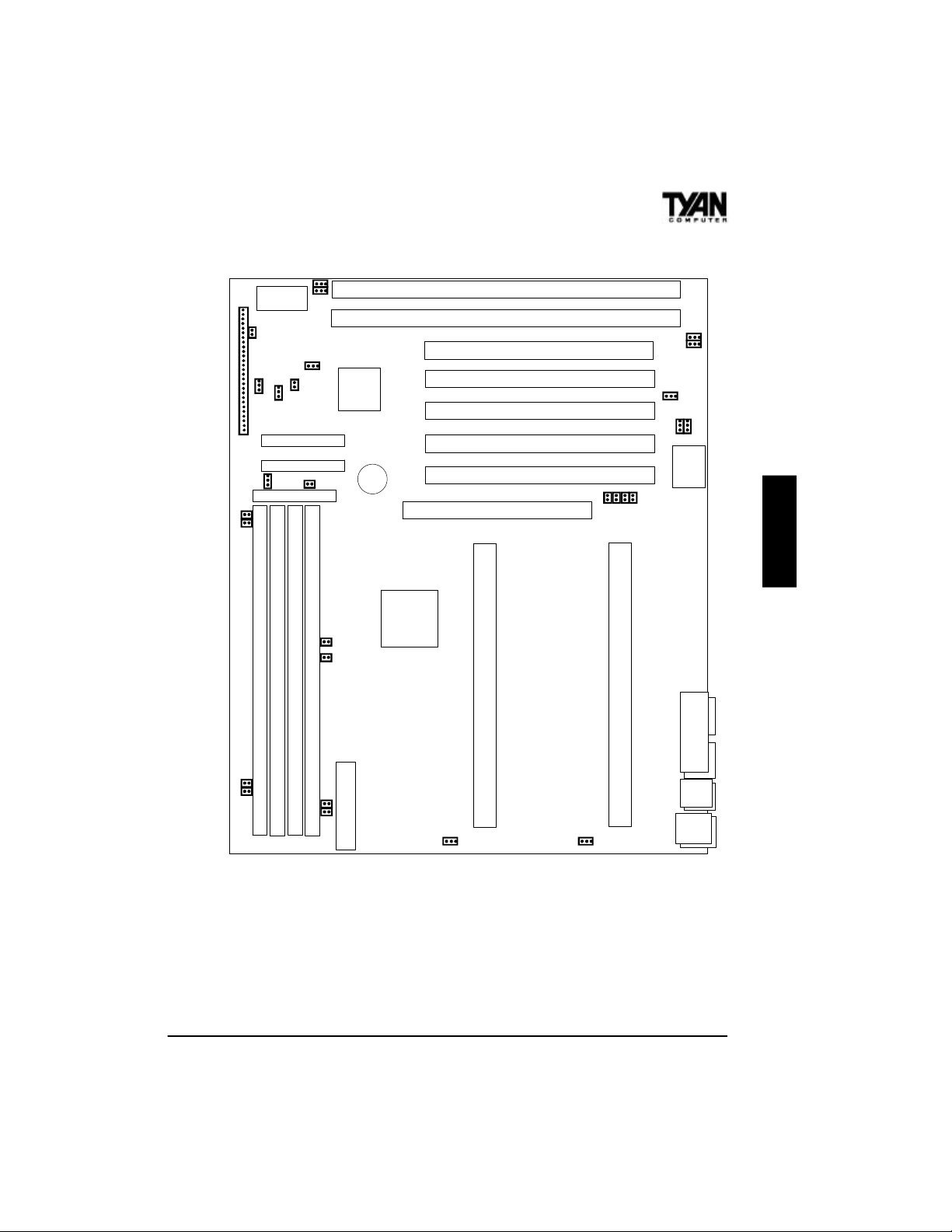
Map of Motherboard Jumpers
1
JP4
1
BIOS
J25
24
J20
22
18
13
CH FAN
10
1
8
3
1
JP3
JP22
JP21
JP5
JP2
JP44
1
JP6
Primary IDE
Secondary IDE
JP43
1
Floppy
1
82371AB
1
1
1
JP15
JP16
3 volt
battery
Intel
82443LX
chip
AGP (Accelerated Graphics Port)
ISA slot 2
ISA slot 1
PCI slot 5
PCI slot 4
PCI slot 3
PCI slot 2
PCI slot 1
1
J18
J19
1
1
JP23
JP41
JP42
1
1
Super I/O
National 309
JP8
JP10
JP7
JP9
ONBOARD
DIMM Bank 3
JP20
JP19
DIMM Bank 2
DIMM Bank 1
DIMM Bank 0
JP18
JP17
power connector
Pentium II CPU Slot 2 (S1692D only)
1 1
FAN
FAN
Pentium II CPU Slot 1
Printer Port
USB2
Mouse
The tiny “1”s next to jumpers of 3 pins or more indicate the position of
pin 1 for that jumper. Refer to pages 14-16 for the jumper and pin
assignments.
13
COM2 COM1
USB1
Keyboard
Chapter 3
Flash BIOS
SB82371AB (PIIX4)
Advanced Programmable Interrupt Controller
for Multiprocessor (S1692D only)
2 PnP ISA slots
PCI slots
National LM78
Accelerated
Graphics Port
National LM75
5 BUS Master
National 309 Super I/O
4 DIMM sockets
Pin Assignments
JP6 (Wake-on LAN)
FAN1-FAN3
(-- indicates pin is absent)
82443LX
Built-in dual VRM with
overload protection
1 2 3
Standby 5V GND Wake (Power-on Active High)
GND VCC Fan Monitor
14
CPU Clock Settings
JP7 JP8 JP9 JP10
233MHz
266MHz
300MHz
*333MHz
ON OFF OFF ON
ON ON ON OFF
ON OFF ON OFF
ON ON OFF OFF
*This speed has not been tested
due to the unavailability of the
CPU at the time of printing.
CMOS Discharge Settings
JP3 Pins
Normal (default)
Clear CMOS
1-2
2-3
Flash Memory Settings
JP4 Pins
5V (default)
12V
1-2
2-3
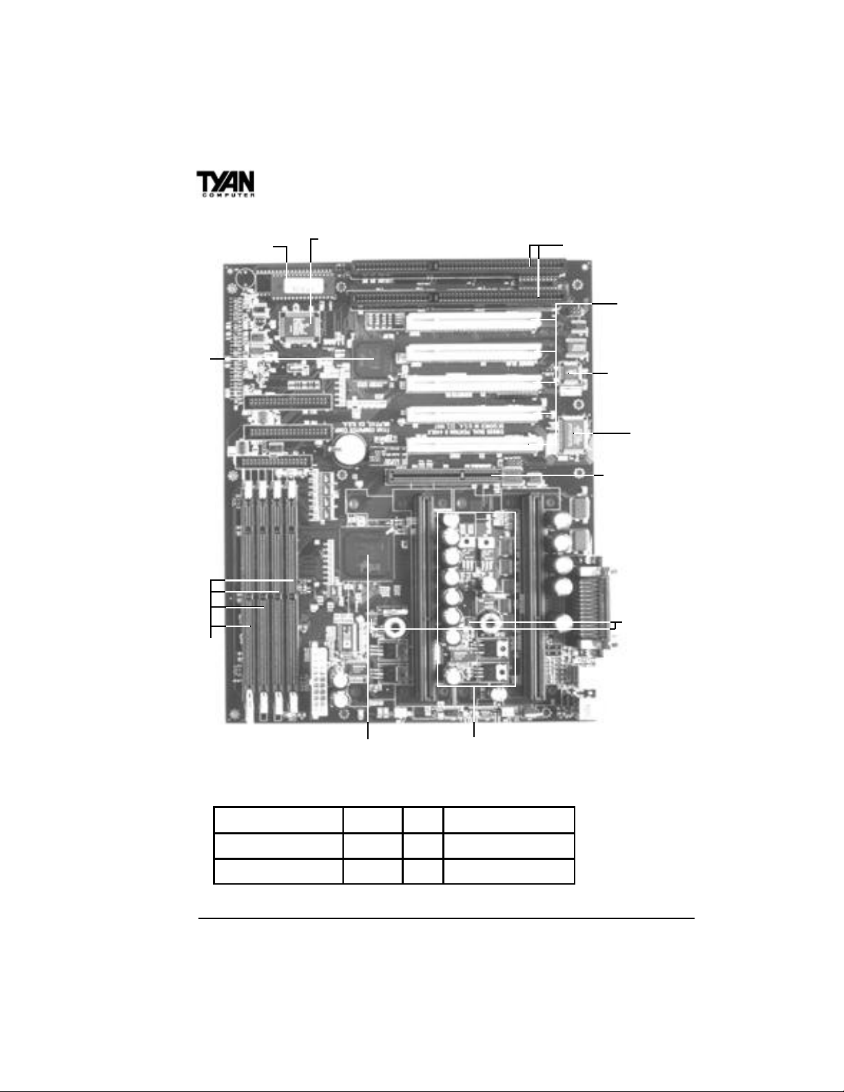
The speed of your CPU is printed on the edge of the
processor. It is a three digit number after “PX”. The
processor shown below is 233MHz.
JP4
JP3
JP21-JP22
JP15-JP16
JP19-JP20
JP17-JP18
JP7-JP10
ONBOARD
DRAM Voltage Settings
JP15 JP16 JP17 JP18 JP19 JP20 JP21 JP22
3.3V
(default)
CLOSED CLOSED CLOSED CLOSED OPEN OPEN OPEN OPEN
OPEN OPEN OPEN OPEN CLOSED CLOSED CLOSED CLOSED
5V
InfraRed Settings
JP41
JP42
JP43
JP44
2 FDD
(default)
1-2 2-3
1-2 2-3
Closed Open
Open Closed
InfraRed
JP44
15
JP43
JP41JP42
Chapter 3
J25 Settings
Pins 1-2 3-4 6-11 13-16 18-20 22-23 24-27
Function
Assignment
Soft Power
On/Off
1=Power
2=GND
Sleep IR Connector HDD LED Power LED Reset Speaker
6=VCC
3=GND
4=Sleep
7=NC
8=IR RX
9=GND
10=IR TX
11=MODE
13=VCC
14=NC
15=-
16=+
18=GND
19=NC
20=+
JP2
22=GND
23=Reset
Soft Power Connector
J25
The Soft Power Connector is
located on pins 1 and 2 of jumper
block J25. Pressing the Soft
Power Button will turn the system
on (and off).
Sleep Button Connector
24=GND
25=NC
26=INT-SPK
27=-
The sleep button connector is located on
pin 3 and pin 4 of jumper block J25. Pressing this button will put the
system in Sleep or Suspend mode. Pressing it once more will wake up the
system. The power LED will blink when the system is in Sleep mode.
A four second override feature is built into the motherboard according to
PC98 specifications. If you hold the sleep button for more than four seconds, the system will shut itself down. Use the four second override feature when the system hangs or crashes. This feature is not intended for
normal shutdown operation. Please use the regular soft power button for
a normal shutdown.
16

Speaker Connector Installation
The S1692S/D provides a 4-pin header to connect the speaker. The
speaker is connected to pins 24-27 of jumper block J25.
Hardware Reset Switch Connector
Installation
The Reset switch on your case’s display panel provides you with the
Hardware Reset function, which is the same as power on/off. The
system will do a cold start after the Reset button is pushed. The Reset
switch is a 2-pin connector and should be installed on pins 22 and 23 of
jumper block J25.
Windows 95 Users:
!
You may encounter problems with some of the devices in the Intel 82371AB
chipset. Neither the PCI Bridge nor the PCI Universal Serial BUS device
IDs for this chipset (also called PIIX4) are recognized by Windows 95.
This is a software problem, not a hardware problem, and can be easily
remedied by either upgrading to Windows 98 or downloading the 82371AB
patch found at http://www.tyan.com or at ftp://download.intel.com/design/pcisets/busmastr/setupex.exe. (Note: USB requires Windows 95 OSR
2.1 or above; please contact Microsoft for the USB update.)
ONBOARD
CMOS RTC
The 440LX AGPset includes an internal
battery and Real Time Clock circuit. The
RTC provides the date and time for the
system. If the battery is low, it will
prevent your system from POSTing, and
you will not get a display. Normally the
life span of an RTC internal battery is 10
years, but if yours is running low, you will
need to replace it with a new 3V lithium
battery (Duracell DL2032).
17
Battery

Chapter 3
Flash EEPROM
The S1692S/D uses flash memory to store BIOS programs. It can be
updated as new versions of the BIOS become available. You can
upgrade your BIOS easily using the flash utility (see page 56).
JP4 determines which type of EPROM is used. This jumper has been
set to match the onboard BIOS chip. The factory default for the
S1692S/D is on pins 1-2. Depending on the type of EPROM used,
some boards will have JP4 on pins 2-3.
Hardware CMOS & Password Reset
If you have been locked out of your system because you forgot your
password or set the CMOS incorrectly, follow the instructions below.
1. Power off the system
2. Set jumper JP3 to pins 2 and 3 (see previous page for
location of JP3).
3. Wait for 2 seconds, then return jumper JP3 to pins 1 and 2.
4. Power on the system again.
By following this procedure, you will erase your password and reset
the CMOS to the BIOS defaults.
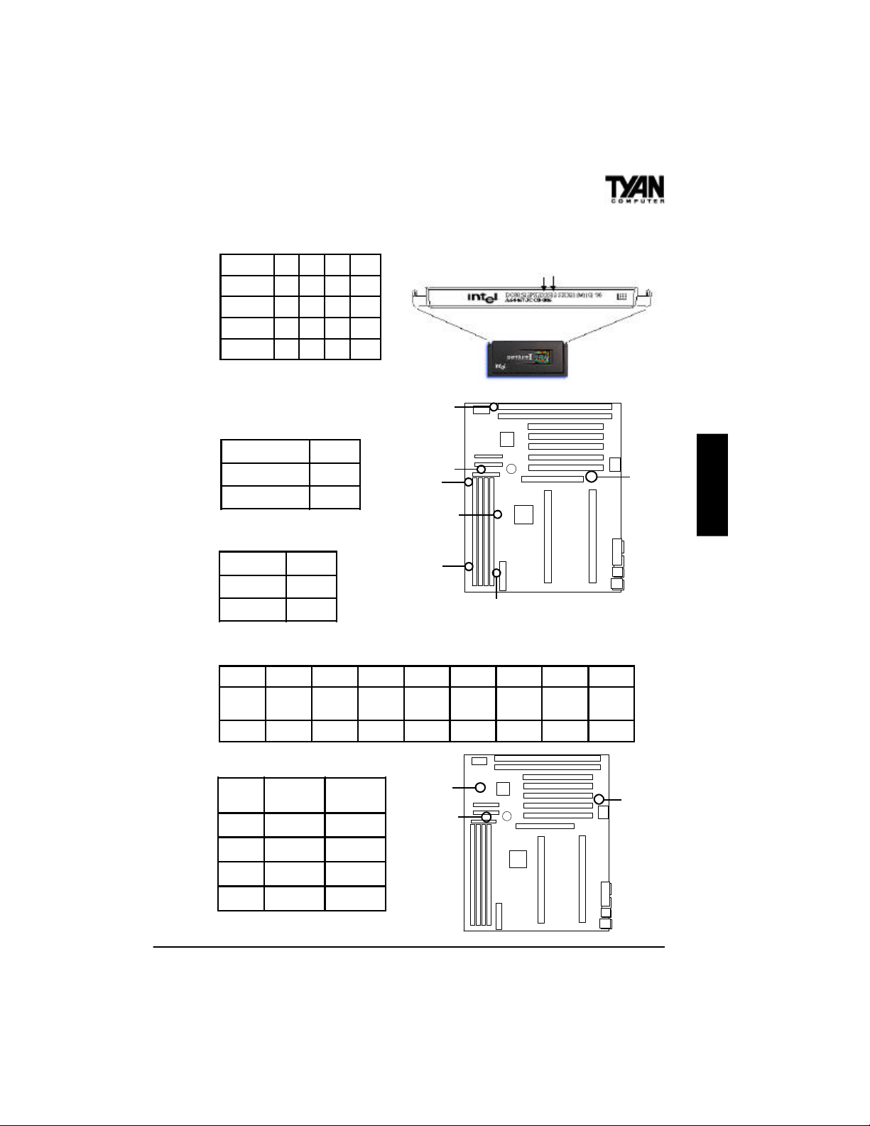
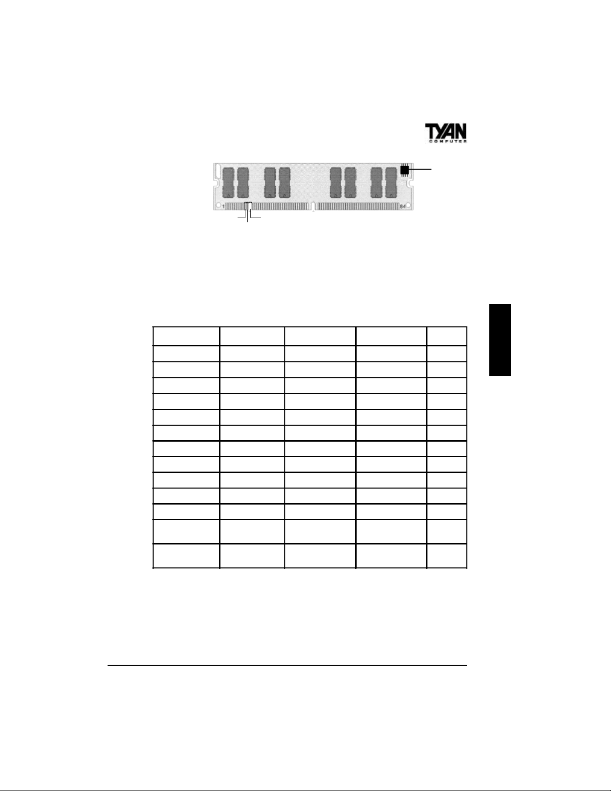
DRAM Installation
The S1692S/D uses a 64-bit data path from memory to CPU and can
accommodate up to 1024MB of EDO RAM and 512MB of SDRAM.
SDRAMs (Synchronous DRAMs) are supported in the DIMM slots.
DIMMs must be of the unbuffered variety. The position of the notch
in the DRAM Key Position will tell you whether or not a DIMM is
unbuffered (see figure on the next page). All installed memory will be
automatically detected, so there is no need to set jumpers. The 440LX
AGPset can cache up to 512MB of RAM.
18
EEPROM
Buffered
Unbuffered
168-pin DIMM
RFU
Some details of memory installation:
s One unbuffered DIMM must be installed for the system to POST.
s The mainboard supports 8MB, 16MB, 32MB, 64MB, 128MB, and
256MB DIMM modules. 256MB DIMM modules must be EDO.
The table below shows some of the possible memory configurations.
DIMM Bank 0 DIMM Bank 1
16MBx1 0 0 0 16MB
16MBx1 16MBx1 0 0 32MB
32MBx1 0 0 0 32MB
16MBx1 16MBx1 16MBx1 0 48MB
32MBx1 32MBx1 0 0 64MB
64MBx1 0 0 0 64MB
32MBx1 32MBx1 32MBx1 0 96MB
16MBx1 16MBx1 32MBx1 32MBx1 96MB
32MBx1 32MBx1 32MBx1 32MBx1 128MB
64MBx1 64MBx1 0 0 128MB
64MBx1 64MBx1 64MB 64MBx1 256MB
128MBx1 128MBx1 128MBx1 128MBx1
256MBx1 256MBx1MBx1 256MBx1 256MBx1
DIMM Bank 2 DIMM Bank 3
Total
512MB
(SDRAM)
1024MB
(EDO only)
ONBOARD
19

Chapter 3
Installing the CPU
Pentium II processors (233 through 333MHz) can be used on the S1692S/
D. Please refer to page 15 for the correct CPU jumper settings for your
board. Although the S1692DL motherboard is designed as a dual CPU
system, it will also function with a single CPU.
The S1692S/D board provides two slots for Pentium II processors, called
the Pentium II primary and secondary slots. If only one CPU is used, that
CPU should be plugged into the primary slot. When two CPUs are used,
they should be of the same speed and type.
Remember:
s The CPU is a sensitive electronic component and it can easily be
damaged by static electricity. Do not touch the CPU pins with your
!
fingers.
s When installing the CPU into the socket, match the CPU pins to
the socket pins. Note that one corner of the socket’s top is different
from the other three corners. Likewise, one corner of the CPU’s
bottom is different from the other three corners. Line the unique
socket corner up with the unique CPU corner.
s Before the CPU is installed, the mainboard must be placed on a
flat surface. You should be able to insert the CPU with minimal,
but firm, pressure. Do not press down hard on the CPU.
Active and Passive Processors
Currently, Intel produces two types of Pentium II processors: the active
(or boxed) processor and the passive processor (refer to the pictures on
the following page). These two types of processors are essentially the
same in design; the only difference lies in their cooling methods. The
active processor is equipped with a cooling fan and heat sink, while
the passive processor is equipped with a heat sink alone. Both types of
CPUs provide the user with the same performance, and both types can
be installed in the Pentium II slots on the S1692S/D board. Refer to
page 21 for instructions regarding the installation and removal of
Pentium II processors.
20
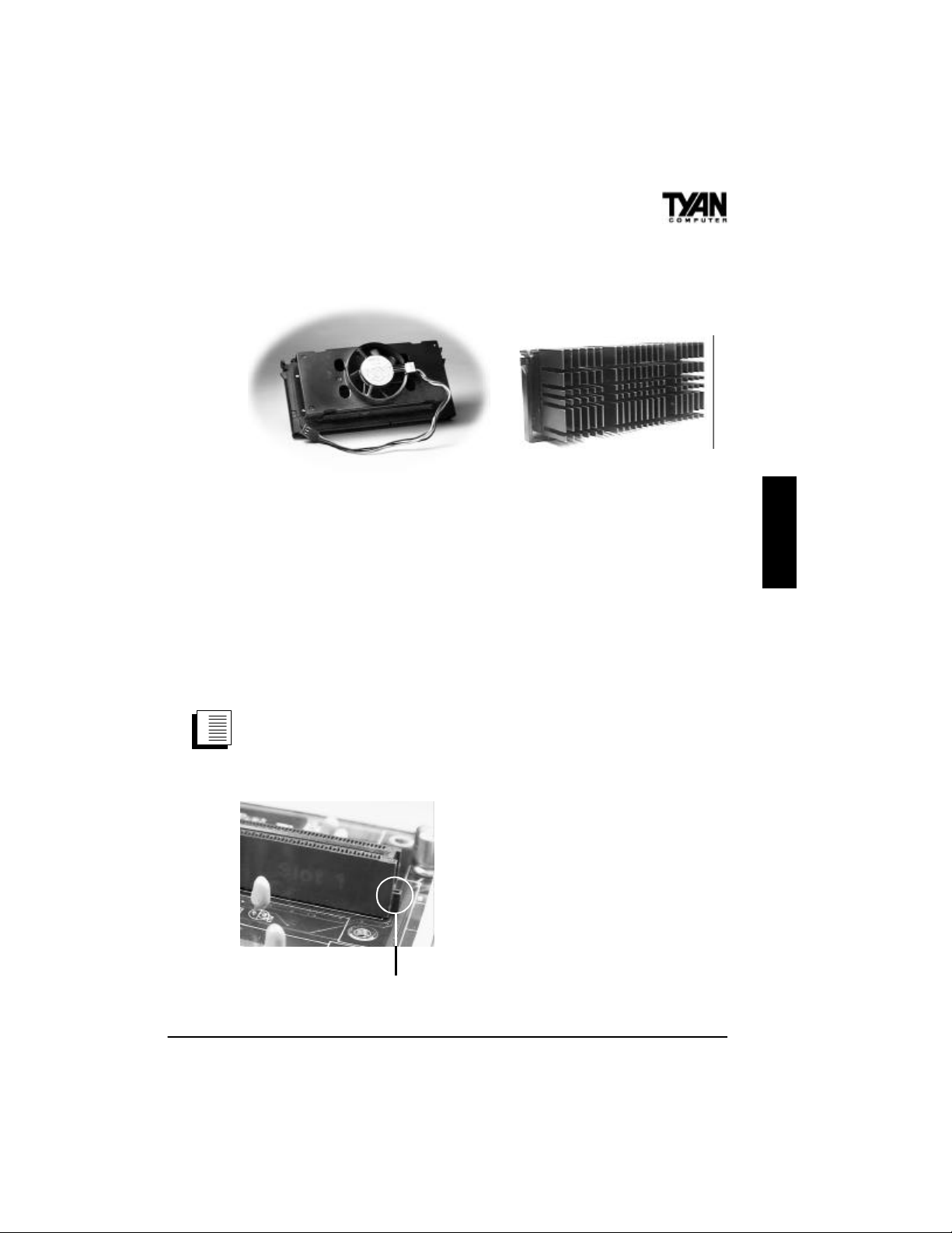
Pentium II Active (Boxed) CPU
Shown with Power Connector for Fan
Pentium II Passive CPU
Shown with Heat-sink
Installation of Pentium II Active (Boxed) Processors
Active processors are equipped with cooling fans. When installing an
active CPU, you also need to connect the cooling fan cable to its
connector.
Installing CPU Retention Modules
1. Installation of a Pentium II active processor requires a CPU
retention module, which is first secured onto the motherboard. (Refer
to the motherboard layout on page 13.)
2. To attach the retention module, place
the motherboard on a flat surface.
3. Locate the key pin on one end of the
Pentium II slot on the board. Then
carefully line up the key notch on the
retention module with the key pin on
the Pentium II slot (the key pin on the
Pentium II slot indicates the correct
Pentium II Slot Connector
and Key Pin
orientation of the CPU).
ONBOARD
21

Chapter 3
4. Drop the retention module down over the
Pentium II slot so that the retention module
sits flat against the motherboard. Tighten the
screws in a clockwise manner to secure the
module to the board. Warning: Do not
overtighten the screws as you may damage
Retention Module
the module and/or the motherboard.
Installing the Active Processor
1. When the retention module is securely installed, you are ready to plug
the CPU into the retention module.
2. Press firmly on the CPU until you hear a
“click.” This clicking sound indicates that the
CPU is fully locked into the retention module.
3. After the CPU is securely seated on the retention module in the Pentium II slot, connect
the CPU’s cooling fan cable to the cooling fan
power connector on the board.
Installing CPU Cooling Fans
1. Locate the cooling fan connectors (3 connectors: FAN1-FAN3) on the
motherboard.
2. Plug the CPU’s cooling fan cable into the cooling fan connector on
the board. Make sure that the black wire of the cable is plugged into
pin 1 of the connector. Refer to pin 1 marked on the layout on page 13.
Pin assignments: pin 1–ground (black), pin 2–12 V (red), pin 3– signal
(yellow).
Installation of Pentium II Passive Processors
Unlike active processors, passive processors are not equipped with
cooling fans. Instead, they are equipped with heat sinks.
22

Each CPU package should contain
the following:
One CPU retention module
One heat sink retention bracket with
Pentium II Passive
CPU Module
mounting locks
Two mounting attach-mounts
One heat sink lock
Installing CPU Retention Modules
1. When installing the CPU retention module, make sure that you have
the appropriate end of the module lined up with the key notch on the
Pentium II slot connector. This will ensure that the module is installed
properly.
2. Before tightening the screws, make certain that the module is flush
against the motherboard. If one end of the module is raised above the
board, check the orientation of the module.
3. Install the module on the board by turning the screws in a clockwise
direction. Do not over-tighten the screws.
ONBOARD
Installing Heat Sink Mounting Brackets
1. The heat sink mount has
two pins on the bottom and
four pins on the top. Notice
that the bottom two pins are
of different sizes. The size of
Heat Sink Mounting
Bracket
the pins and the holes in the
motherboard will determine the correct orientation. A correctly installed
bracket can be verified by making sure that the four pins on the top are
closest to the Pentium II CPU slot.
23

Chapter 3
2. Insert the heat sink mount into the holes on the motherboard. When
the bracket is properly inserted into the holes on the motherboard, you
will hear a clicking noise.
3. Lock the heat sink mount to the board by
inserting the two mounting locks into the pins
of the heat sink mounting bracket which are
now below the mainboard. There will be a
click when the locks are securely fastened.
Installing the Passive Processor
Mounting Locks
1. Align the CPU with the CPU retention module. Make sure the heat
sink is lined up with the heat sink mount bracket. If you put the CPU in
the wrong way, you may damage the CPU, the motherboard, and/or the
CPU socket.
2. Slowly press down on the CPU module until the CPU locks into
place. A clicking noise will be heard when the CPU is locked securely
into the module.
Installing Heat Sink Locks
The heat sink lock has four notches which will correspond to the four
pins on the heat sink mounting bracket. Gently slide the lock between
the heat sink onto the heat sink
mounting bracket until both sides of
the lock are firmly secured. A
Heat Sink Lock
clicking sound will be heard when
the lock is securely fastened to the
heat sink mounting bracket. To
remove the lock from the heat sink mounting bracket, gently press the
ends of the locks inward and pull.
24

Removing Pentium II Passive Processors and CPU Retention
Modules
To remove the CPU, move the locks to the center of the CPU. A click
will be heard when the CPU has been unlocked. Gently pull up on the
CPU, taking care not to bend the motherboard or the CPU retention
module.
Removing Heat Sink Locks
To remove the lock from the retention bracket, gently press the ends of
the locks inward and pull.
Peripheral Device Installation
After all the jumpers on the mainboard have been set, the mainboard
can be mounted into the case. You may then install the display card
and any other peripheral devices that you may have.
If a PCI-BUS interface card is to be installed in the system, any one of
the four PCI-BUS slots can support either a Master or a Slave device.
After installing the peripheral controllers, you should check the CPU
and all of your devices again before preparing to power on the system.
Connecting the Power Supply
The female power supply connector on the mainboard fits with the
male power supply connector from a 3.3V, 5V, or 12V power supply.
Beware: incorrect installation of the power supply can result in serious
damage to the system board and connected peripherals. Before connecting the leads from the power supply, you should first make sure that
the power supply is unplugged.
ONBOARD
25

Chapter 3
Most male power supply connectors will have twenty wires, seven of
which are black. The black wires will be in the middle of the connector.
The easiest way to orient the connectors properly is to line up the
plastic clip on the male connector with the tab on the female connector.
The plastic clip should be facing the edge of the motherboard.
Align the plastic guide pins on the male connector with their receptacles on the mainboard. You may need to hold the lead at an angle in
order to properly line it up with the onboard connector. Once you have
the guide pins aligned, press the lead into the connector so that the
plastic clip on the lead snaps into place and secures the lead to the
connector. Please see the figure below.
Power supply connector
Onboard connector
clip
tab
26

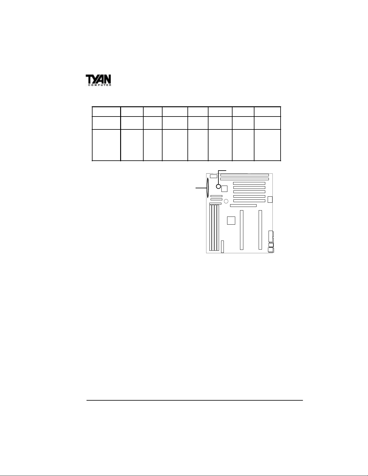
Frequently Asked Questions
Q: Why don’t I get a display after I put in my old DIMM module?
A: The 440LX chipset requires the memory manufacturer to program
an EEPROM chip with SPD (Serial Presence Detection) on the
module in order for the BIOS to program the 440LX’s timing registers
properly. Your DIMM may not have the EEPROM chip on the module,
or the EEPROM may not contain the correct program. Check with
your memory vendor for details. The figure below shows a DIMM
module with an EEPROM chip.
EEPROM
ONBOARD
RFU
Buffered
Unbuffered
168-pin DIMM
Q: My system sometimes becomes unstable. How should I check the
system?
A: The first thing to do is to check and see if you have any device
conflict in address, IRQ, or DMA. If you are using Windows 95, the
Device Manager is a good place to start. Please consult your operating
system manual for detail. Second of all, slowing down the memory
timing in the BIOS’s chipset setup section will help the situation, as
well. Many memory modules are not suitable for high performance
systems and are probably the main source of your problem.
Q: I’ve installed Windows NT with one CPU and with the multiproces-
sor kernel. However, when I add a second CPU later, only one CPU is
detected during the Windows NT boot up.
A: AMI BIOS only builds multiprocessor tables according to the
number of CPUs present during Windows NT installation. Therefore,
you must either reinstall NT with two CPUs or use the Windows NT
resources kit to change from a uniprocessor to a multiprocessor
system.
27

Q: How do I know if the system detects the number of CPUs
properly?
A: The AMI BIOS will show a “Pentium–II x2” message during the
memory check to indicate the presence of two CPUs.
Q: How many devices can I hook up to each SCSI channel?
A: You can cascade up to fifteen 16-bit devices per channel and seven
of them can be 8-bit devices.
Q: How do I use the RAID port on my motherboard?
A: The RAID port allows you to put in an Adaptec Array 1000 family
card which will enable the SCSI chip on the motherboard to perform
the RAID function under Netware and Windows NT. RAID 0 is used
for performance purposes (increases SCSI speed), RAID 1 is used for
mirroring (creates two drives with identical information), and RAID 5 is
used for redundancy (if one drive goes down, another will take its
place).
Q: Can I mix EDO DIMM with SDRAM DIMM on this
motherboard?
A: Yes. However, the AGP graphics card performs better with
SDRAM installed on the motherboard because the AGP card can store
the texture map in the system memory.
Q: What is AGP (Accelerated Graphics Port)?
A: AGP (Accelerated Graphics Port) is a new BUS architecture for
3D graphics. The AGP slot eliminates the PCI bandwidth bottleneck by
bypassing the PCI interface and accessing the system memory directly.
Currently, the AGP supports 1X and 2X which yields bandwidths of
256MB/s at 66MHz and 512MB/s at 133MHz BUS speeds, respectively. Compare with 132MB/s at 33MHz bus speed with PCI bus.
28

Q: Does my operating system support AGP?
A: Currently, only Windows 98 and Windows NT 5.0 will have built-in
support for AGP. Some AGP cards require Windows 95 OSR2.1 or a
special driver from Intel. Please check with your graphics vendor for
more detail.
29

Chapter 4
chapter 4
BIOS Configuration
Standard Setup
Select the AMIBIOS Setup options below by choosing Standard Setup
from the AMIBIOS Setup main menu. Standard Setup options are
described below.
Floppy Drive A: and B:
Move the cursor to these fields via the arrow keys and select the floppy
type. The settings are 360KB 5¼ inch, 1.2 MB 5¼ inch, 720KB 3½
inch, 1.44MB 3½ inch, or 2.88MB 3½ inch.
Primary Master, Primary Slave, Secondary Master, Secondary
Slave
Select these options to configure the drive named in the option. Select
Auto Detect IDE to let AMIBIOS automatically configure the drive. A
screen with a list of drive parameters appears. Click on OK to configure the drive.
30

Type How to Configure
SCSI
IDE
CD-ROM
Standard MFM
Non-Standard MFM
Select Type. Select Not Installed on the drive parameter screen. The
SCSI drivers provided by the SCSI manufacturer should allow you to
configure the SCSI drive.
Select Type. Select Auto to let AMIBIOS determine the parameters.
Click on OK when AMIBIOS displays the drive parameters. Select
LBA Mode. Select On if the drive has a capacity greater than
540MB.
Select Block Mode. Select On to allow block mode data transfers.
Select 32-Bit Mode. Select On to allow 32-bit data transfers. Select
the PIO Mode. It is best to select Auto to allow AMIBIOS to
determine the PIO mode. If you select a PIO mode that is not
supported by the IDE drive, the drive will not work properly. If you
are absolutely certain that you know the drive's PIO mode, select PIO
mode 0-4, as appropriate.
Select Type. Select CDROM. Click on OK when AMIBIOS displays
the drive parameters.
Select Type. You must know the drive parameters. Select the drive
type that exactly matches your drive's parameters.
Select Type. If the drive parameters do not match the drive
parameters listed for drive types 1-46, select User and enter the
correct hard disk drive parameters.
Entering Drive Parameters
You can also enter the hard disk drive parameters yourself. The drive
parameters are as follows:
Parameter Description
Type The number for a drive with certain identification parameters.
Cylinders The number of cylinders in the disk drive.
Heads The number of heads.
The actual physical size of a sector gets progressively smaller as the
track diameter diminishes. Yet each sector must still hold 512 bytes.
Write Precompensation
Landing Zone
Sectors
Capacity
Write precompensation circuitry on the hard disk compensates for the
physical difference in sector size by boosting the write current for
sectors on inner tracks. This parameter is the track number on the
disk surface where write precompensation begins.
This number is the cylinder location where the heads normally park
when the system is shut down.
The number of sectors per track. MFM drives have 17 sectors per
track. RLL drives have 26 sectors per track. ESDI drives have 34
sectors per track. SCSI and IDE drives have even more sectors per
track.
The formatted capacity of the drive is the number of heads times the
number of cylinders times the number of sectors per track times 512
(bytes per sector).
BIOS
31

Chapter 4
Type Cylinders Heads
1 306 4 128 305 17 10 MB
2 615 4 300 615 17 20 MB
3 615 6 300 615 17 31 MB
4 940 8 512 940 17 62 MB
5 940 6 512 940 17 47 MB
6 615 4 65535 615 17 20 MB
7 462 8 256 511 17 31 MB
8 733 5 65535 733 17 30 MB
9 900 15 65535 901 17 112 MB
10 820 3 65535 820 17 20 MB
11 855 5 65535 855 17 35 MB
12 855 7 65535 855 17 50 MB
13 306 8 128 319 17 20 MB
14 733 7 65535 733 17 43 MB
16 612 4 0 663 17 20 MB
17 977 5 300 977 17 41 MB
18 977 7 65535 977 17 57 MB
19 1024 7 512 1023 17 60 MB
20 733 5 300 732 17 30 MB
21 733 7 300 732 17 43 MB
22 733 5 300 733 17 30 MB
23 306 4 0 336 17 10 MB
24 925 7 0 925 17 54 MB
25 925 9 65535 925 17 69 MB
26 754 7 754 754 17 44 MB
27 754 11 65535 754 17 69 MB
28 699 7 256 699 17 41 MB
29 823 10 65535 823 17 68 MB
30 918 7 918 918 17 53 MB
31 1024 11 65535 1024 17 94 MB
32 1024 15 65535 1024 17 128 MB
33 1024 5 1024 1024 17 43 MB
34 612 2 128 612 17 10 MB
35 1024 9 65535 1024 17 77 MB
36 1024 8 512 1024 17 68 MB
37 615 8 128 615 17 41 MB
38 987 3 987 987 17 25 MB
39 987 7 987 987 17 57 MB
40 820 6 820 820 17 41 MB
41 977 5 977 977 17 41 MB
511 981 5 981 981 17 41 MB
43 830 7 512 830 17 48 MB
44 830 10 65535 830 17 69 MB
45 917 15 65535 918 17 114 MB
46 1224 15 65535 1223 17 152 MB
Write
Precompensation
Landing
Zone
Sectors Capacity
32

Advanced Setup
The Advanced Setup options included in the AMIBIOS Setup generated through AMIBCP and the AMIBIOS for the Intel 440LX chipset
are described in this chapter. Select Advanced Setup from the
AMIBIOS Setup main menu to display the Advanced Setup options.
Default Settings
Every option in AMIBIOS Setup contains two default values: an FailSafe default and the Optimal default value.
Optimal Defaults
The Optimal default values provide optimum performance settings for
all devices and system features.
Fail-Safe Defaults
The Fail-Safe default settings consist of the safest set of parameters.
Use them if the system is behaving erratically. They should always
work but do not provide optimal system performance characteristics.
Advanced Setup
Quick Boot
Set this option to Enabled to instruct AMIBIOS to boot quickly when
the computer is powered on. This option replaces the old Above 1 MB
Memory Test Advanced Setup option. The settings are:
Setting Description
AMIBIOS tests all system memory.
AMIBIOS waits up to 40 seconds for a READY signal from the IDE hard disk drive. AMIBIOS waits for .5
Disabled
seconds after sending a RESET signal to the IDE drive to allow the IDE drive time to get ready again.
AMIBIOS checks for a <Del> key press and runs AMIBIOS Setup if the key has been pressed.
AMIBIOS does not test system memory above 1MB.
AMIBIOS does not wait up to 40 seconds for a READY signal from the IDE hard disk drive. If a READY signal
is not received immediately from the IDE drive, AMIBIOS does not configure that drive. AMIBIOS does not
Enabled
wait for .5 seconds after sending a RESET signal to the IDE drive to allow the IDE drive time to get ready again.
You cannot run AMIBIOS Setup at system boot, because there is no delay for the Hit <Del> to run Setup
message.
The Optimal and Fail-Safe default settings are Disabled.
BIOS
33

Chapter 4
1st Boot Device
This option sets the type of device for the first boot drives that the
AMIBIOS attempts to boot from after AMIBIOS POST completes.
The settings are Disabled, Network, Floptical, SCSI, CDROM, IDE-0,
IDE-1, IDE-2, or IDE-3. The Optimal and Fail-Safe default settings are
IDE-0.
2nd Boot Device
This option sets the type of device for the second boot drives that the
AMIBIOS attempts to boot from after AMIBIOS POST completes.
The settings are Disabled, Floppy, Floptical, CDROM, or IDE-0. The
Optimal and Fail-Safe default settings are Floppy.
3rd Boot Device
This option sets the type of device for the third boot drives that the
AMIBIOS attempts to boot from after AMIBIOS POST completes.
The settings are Disabled, Floptical, Floppy, CDROM, or IDE-0. The
Optimal and Fail-Safe default settings are CD-ROM.
Try Other Boot Devices
Set this option to Yes to instruct AMIBIOS to attempt to boot from any
other drive in the system if it cannot find a boot drive among the drives
specified in the 1st Boot Device, 2nd Boot Device, and 3rd Boot
Device options. The settings are Yes or No. The Optimal and Fail-Safe
default settings are Yes.
Initial Display Mode
This option specifies the initial display mode when the system boots.
The settings are as follows:
Setting Description
BIOS The messages that AMIBIOS displays before booting the system will appear on the system monitor.
Silent The messages that AMIBIOS displays will not appear on the system monitor.
34

Display Mode At Add-On ROM Init
This option specifies the system display mode that is set at the time
that AMIBIOS POST initializes an optional option ROM. The settings
are as follows:
Setting Description
Force BIOS The display mode currently being used by AMIBIOS is used.
Keep Current The current display mode is used.
Floppy Access Control
This option specifies the read/write access that is set when booting
from a floppy drive. The settings are Read/Write or Read-Only. The
Optimal and Fail-Safe default settings are Read/Write.
Hard Disk Access Control
This option specifies the read/write access that is set when booting
from a hard disk drive. The settings are Read/Write or Read-Only. The
Optimal and Fail-Safe default settings are Read/Write.
S.M.A.R.T. For Hard Disks
Set this option to Enabled to permit AMIBIOS to use the SMART
(System Management and Reporting Technologies) protocol for
reporting server system information over a network. Enabling this
feature allows you to back up your data when your hard disk is about
to fail. The settings are Enabled or Disabled. The Optimal and FailSafe default settings are Disabled.
BIOS
Boot Up Num Lock
Set this option to Off to turn the Num Lock key off when the computer
is booted so you can use the arrow keys on both the numeric keypad
and the keyboard. The settings are On or Off. The default settings are
On.
35

Chapter 4
PS/2 Mouse Support
Set this option to Enabled to enable AMIBIOS support for a PS/2-type
mouse. The BIOS will allocate IRQ12 for the PS/2 mouse. The settings
are Enabled or Disabled. The Optimal and Fail-Safe default settings
are Enabled.
Primary Display
This option configures the type of monitor attached to the computer.
The settings are Mono, CGA40x25, CGA80x25, VGA/EGA, or
Absent. The Optimal and Fail-Safe default settings are VGA/EGA.
Password Check
This option enables password checking every time the system boots or
when you run AMIBIOS Setup. If Always is chosen, a user password
prompt appears every time the computer is turned on. If Setup is
chosen, the password prompt appears if AMIBIOS is executed. See the
Advanced Setup chapter for instructions on changing a password. The
Optimal and Fail-Safe defaults are Setup.
Boot To OS/2
Set this option to Enabled if running OS/2 operating system and using
more than 64 MB of system memory on the motherboard. The settings
are Enabled or Disabled. The Optimal and Fail-Safe default settings
are Disabled.
CPU Microcode Update
Set this option to Enabled to permit the BIOS to update the CPU at any
time. The settings are Enabled or Disabled. The Optimal and Fail-Safe
default settings are Enabled.
Internal Cache
This option sets the type of caching algorithm used by the L1 internal
cache memory on the CPU. The settings are WriteBack, WriteThru, or
Disabled. The Optimal and Fail-Safe default settings are Disabled.
36

System BIOS Cacheable
When set to Enabled, the contents of the F0000h system memory
segment can be read from or written to cache memory. The contents of
this memory segment are always copied from the BIOS ROM to
system RAM for faster execution. The settings are Enabled or Disabled. The Optimal default setting is Enabled. The Fail-Safe default
setting is Disabled.
C000,16K Shadow and C400,16K Shadow
These options specify how the 32 KB of video ROM at C0000h is
treated. The settings are:
Setting Description
Disabled The contents of the video ROM are not copied to RAM.
Enabled
Cached
The contents of the video ROM area from C000h-C7FFFh are copied (shadowed) from ROM to
RAM for faster execution.
The contents of the video ROM area from C000h-C7FFFh are copied from ROM to RAM and can
be written to or read from cache memory.
The Optimal and Fail-Safe default settings are Cached.
C800,16K Shadow; CC00,16K Shadow; D000,16K Shadow;
D400,16K Shadow; D800, 16K Shadow; and DC00,16K Shadow
These options enable shadowing of the contents of the ROM area
named in the option. The ROM area not used by ISA adapter cards is
allocated to PCI adapter cards. The settings are:
BIOS
Setting Description
Disabled The contents of the video ROM are not copied to RAM.
Enabled
Cached
The contents of the video ROM area from C000h-C7FFFh are copied (shadowed) from ROM to
RAM for faster execution.
The contents of the video ROM area from C000h-C7FFFh are copied from ROM to RAM and can
be written to or read from cache memory.
The Optimal and Fail-Safe default settings are Cached.
37

Chapter 4
Chipset Setup
Choose Chipset Setup on the AMIBIOS Setup main menu. All Chipset
Setup options are then displayed. AMIBIOS Setup can be customized.
AMIBIOS Setup can be customized via AMIBCP. See the AMIBIOS
Utilities Guide for additional information.
USB Function
Set this option to Enabled to enable USB (Universal Serial Bus)
support. The settings are Enabled or Disabled. The Optimal and FailSafe default settings are Enabled.
USB Keyboard/Mouse Legacy Support
Set this option to Enabled to enable support for older keyboards and
mouse devices if the USB Function option is set to Enabled. The
settings are Enabled or Disabled. The Optimal and Fail-Safe default
settings are Disabled.
EDO DRAM Speed (ns)
This option specifies the RAS Access Time in nanoseconds for the
EDO DRAM system memory installed in this computer. The settings
are Auto (AMIBIOS automatically determines the RAS access Time
parameter), Manual, 50, 60, or 70. The Optimal and Fail-Safe default
settings are Auto.
EDO Read Burst Timing
This option specifies the timings for EDO DRAM system memory for
Read operations in burst mode. The settings are x222 or x333. The
Optimal and Fail-Safe default settings are x333. Setting this switch
incorrectly may result in system failure.
EDO Write Burst Timing
This option specifies the timings for EDO DRAM system memory for
Write operations in burst mode. The settings are x222 or x333. The
Optimal and Fail-Safe default settings are x333. Setting this switch
incorrectly may result in system failure.
38

EDO RAS Precharge
This option specifies the length of the RAS precharge part of the
DRAM system memory access cycle when EDO DRAM system
memory is installed in this computer. The settings are 3 CLKs or 4
CLKs. The Optimal and Fail-Safe default settings are 4 CLKs.
EDO RAS To CAS
This option specifies the length of the delay inserted between the RAS
and CAS signals of the DRAM system memory access cycle when
EDO DRAM system memory is installed in this computer. The settings
are 2 CLKs or 3 CLKs. The Optimal and Fail-Safe default settings are
3 CLKs.
MA Wait State
This option specifies the length of the delay inserted between MA
signals. The settings are Slow or Fast. The Optimal and Fail-Safe
default settings are Slow.
SDRAM Timing Latency
This option specifies the latency for the Synchronous DRAM system
memory signals. The settings are Auto (AMIBIOS automatically
determines the optimal delay) or Manual. The Optimal and Fail-Safe
default settings are Auto.
BIOS
RAS To CAS
This option specifies the length of the delay inserted between the RAS
and CAS signals of the DRAM system memory access cycle. The
settings are 2 CLKs or 3 CLKs. The Optimal and Fail-Safe default
settings are 3 CLKs.
CAS Lat.
This option sets the latency period for the CAS signal. The settings are
2 CLKs or 3 CLKs. The Optimal and Fail-Safe default settings are 3
CLKs.
39

Chapter 4
RAS Precharge
This option specifies the length of the RAS precharge part of the
DRAM system memory access cycle when EDO DRAM system
memory is installed in this computer. The settings are 3 CLKs or 4
CLKs. The Optimal and Fail-Safe default settings are 4 CLKs.
VGA Frame Buffer USWC
Set this option to Enabled to enable the VGA video frame buffer using
USWC (Uncacheable, Speculatable, Write-Combined) memory. The
settings are Enabled or Disabled. Older ISA VGA card drivers may not
behave correctly if this option is not set to Disabled. The Optimal and
Fail-Safe default settings are Disabled.
PCI Frame Buffer USWC
Set this option to Enabled to enable the USWC memory attribute and
improve video performance when a PCI video adapter is installed.
However, some VGA card drivers may not behave correctly when this
option is set to Enabled. The settings are Disabled or Enabled. The
Optimal and Fail-Safe defaults are Disabled.
DRAM Integrity Mode
This option sets the type of system memory checking. The settings are:
Setting Description
Non ECC No error checking or error reporting is done.
Multibit errors are detected and reported as parity errors. Single-bit errors are
ECC Only
ECC
corrected by the chipset. Corrected bits of data from memory are not written back to
DRAM system memory. If Level I is selected, the J25 External SMI software jumper
on the Series 745 board is disabled.
Multibit errors are detected and reported as parity errors. Single bit errors are corrected
by the chipset and are written back to DRAM system memory. If a soft (correctable)
memory error occurs, writing the fixed data back to DRAM system memory will resolve
the problem. If a hard (uncorrectable) error occurs, writing the fixed data back to
DRAM system memory does not solve the problem. In this case, the second time the
error occurs in the same location, a parity error is reported, indicating an uncorrectable
error. If ECCI is selected, AMIBIOS automatically enables the System Management
Interface (SMI). If you do not want to enable power management, set the Power
Management/APM option to Disabled and set all Power Management Setup timeout
options to Disabled. To enable power management, set Power Management/APM to
Enabled and set the Power Management Setup timeout options as desired.
40

Fixed Memory Hole
This option specifies the location of an area of memory that cannot be
addressed on the ISA bus. The settings are Disabled, 15 MB-16 MB, or
512KB-640KB. The Optimal and Fail-Safe default settings are Disabled.
TypeF DMA BufferControl1 and TypeF DMA Buffer Control2
These options specify the DMA channel where TypeF buffer control is
implemented. The settings are Disabled, Channel-0, Channel-1,
Channel-2, Channel-3, Channel-5, Channel-6, or Channel-7. The
Optimal and Fail-Safe default settings are Disabled.
DMA-0 Type, DMA-1 Type, DMA-2 Type, DMA-3 Type, DMA-5
Type, DMA-6 Type, DMA-7 Type
These options specify the bus that the specified DMA channel can be
used on. The settings are PC/PCI, Distributed, or Normal ISA. The
Optimal and Fail-Safe default settings are Normal ISA.
AGP Aperture Size
This option specifies the amount of system memory that can be used
by the Accelerated Graphics Port (AGP). The settings are 4 MB, 8 MB,
16 MB, 32 MB, 64 MB, 128 MB, or 256 MB. The Optimal and FailSafe default settings are 256 MB.
BIOS
System Type
This option sets the system type. The settings are Auto (AMIBIOS
automatically determines the system type), DP, or UP. The Optimal
and Fail-Safe default settings are Auto.
41

Chapter 4
USWC Write I/O Post
This option sets the status of USWC posted writes to I/O. The settings
are:
Setting Description
Enabled USWC posted writes to I/O are enabled.
Disabled USWC posted writes to I/O are disabled.
AMIBIOS automatically determines if USWC posted writes to I/O should be enabled and sets this
Auto
option accordingly.
The Optimal and Fail-Safe default settings are Auto.
MECC Buf. Strength
This option sets the strength of the signal for the MECC buffer. The
settings are Auto (AMIBIOS automatically determines the correct
setting), 42mA, 38mA, or 33mA. The Optimal and Fail-Safe default
settings are Auto.
MD Buf. Strength
This option sets the strength of the signal for the MD buffer. The
settings are Auto (AMIBIOS automatically determines the correct
setting), 42mA, 38mA, or 33mA. The Optimal and Fail-Safe default
settings are Auto.
WE Buf. Strength
This option sets the strength of the signal for the WE buffer. The
settings are Auto (AMIBIOS automatically determines the correct
setting), 42mA, 38mA, or 33mA. The Optimal and Fail-Safe default
settings are Auto.
MAX Buf. Strength
This option sets the strength of the signal for the MAX buffer. The
settings are Auto (AMIBIOS automatically determines the correct
setting), 42mA, 38mA, or 33mA. The Optimal and Fail-Safe default
settings are Auto.
MA Buf. Strength
This option sets the strength of the signal for the MA buffer. The
42

settings are Auto (AMIBIOS automatically determines the correct
setting), 48mA, 42mA, or 22mA. The Optimal and Fail-Safe default
settings are Auto.
SCAS3 Buf. Strength
This option sets the strength of the signal for the SCAS3 buffer. The
settings are Auto (AMIBIOS automatically determines the correct
setting), 48mA, 42mA, or 22mA. The Optimal and Fail-Safe default
settings are Auto.
SCAS2:0 Buf. Strength
This option sets the strength of the signal for the SCAS2:0 buffer. The
settings are Auto (AMIBIOS automatically determines the correct
setting), 42mA, 38mA, or 33mA. The Optimal and Fail-Safe default
settings are Auto.
SRAS3 Buf. Strength
This option sets the strength of the signal for the SRAS3 buffer. The
settings are Auto (AMIBIOS automatically determines the correct
setting), 48mA, 42mA, or 22mA. The Optimal and Fail-Safe default
settings are Auto.
BIOS
SRAS2:0 Buf. Strength
This option sets the strength of the signal for the SRAS2:0 buffer. The
settings are Auto (AMIBIOS automatically determines the correct
setting), 48mA, 42mA, or 22mA. The Optimal and Fail-Safe default
settings are Auto.
DQMX5 Buf. Strength
This option sets the strength of the signal for the DQMX5 buffer. The
settings are Auto (AMIBIOS automatically determines the correct
setting), 42mA, 38mA, or 33mA. The Optimal and Fail-Safe default
settings are Auto.
DQMX1 Buf. Strength
This option sets the strength of the signal for the DQMX1 buffer. The
settings are Auto (AMIBIOS automatically determines the correct
43

Chapter 4
setting), 42mA, 38mA, or 33mA. The Optimal and Fail-Safe default
settings are Auto.
DQM Buf. Strength
This option sets the strength of the signal for the DQM buffer. The
settings are Auto (AMIBIOS automatically determines the correct
setting), 42mA, 38mA, or 33mA. The Optimal and Fail-Safe default
settings are Auto.
CSX Buf. Strength
This option sets the strength of the signal for the CSX buffer. The
settings are Auto (AMIBIOS automatically determines the correct
setting), 48mA, 42mA, or 22mA. The Optimal and Fail-Safe default
settings are Auto.
CS7:6 Buf. Strength
This option sets the strength of the signal for the CS7:6 buffer. The
settings are Auto (AMIBIOS automatically determines the correct
setting), 48mA, 42mA, or 22mA. The Optimal and Fail-Safe default
settings are Auto.
CS5:0 Buf. Strength
This option sets the strength of the signal for the CS5:0 buffer. The
settings are Auto (AMIBIOS automatically determines the correct
setting), 48mA, 42mA, or 22mA. The Optimal and Fail-Safe default
settings are Auto.
PAC Bus SERR#
Set this option to Enabled to enable the SERR# signal on the PAC bus.
The settings are Enabled or Disabled. The Optimal and Fail-Safe
default settings are Enabled.
AGP Common SERR#
Set this option to Enabled to permit a common SERR# signal for AGP
and the standard PC bus. The settings are Enabled or Disabled. The
Optimal and Fail-Safe default settings are Enabled.
44

AGP System Error Forwarding
Set this option to Enabled to enable AGP system errors to be forwarded. The settings are Enabled or Disabled. The Optimal and FailSafe default settings are Enabled.
AGP Parity Error Response
Set this option to Enabled to enable AGP parity error response. The
settings are Enabled or Disabled. The Optimal and Fail-Safe default
settings are Enabled.
IRQ12
This option specifies how IRQ12 is used. The settings are:
Setting Description
Auto AMIBIOS automatically determines how IRQ12 should be allocated.
Standard IRQ12 is made available for use on the ISA BUS.
Mouse IRQ12 is used by the PS/2 mouse.
The Optimal and Fail-Safe default settings are Auto.
PIIX4 SERR#
Set this option to Enabled to enable the SERR# signal for the Intel
PIIX4 chip. The settings are Enabled or Disabled. The Optimal and
Fail-Safe default settings are Disabled.
BIOS
USB Passive Release Enable
Set this option to Enabled to enable passive release for USB. The
settings are Enabled or Disabled. The Optimal and Fail-Safe default
settings are Disabled.
PIIX4 Passive
Set this option to Enabled to enable passive release for the Intel PIIX4
chip. The settings are Enabled or Disabled. The Optimal and Fail-Safe
default settings are Enabled.
PIIX4 Delayed Transaction
Set this option to Enabled to enable delayed transactions for the Intel
45

Chapter 4
PIIX4 chip. The settings are Enabled or Disabled. The Optimal and
Fail-Safe default settings are Enabled.
Master Lat. Timer
This option specifies the latency for the Timer. The settings are 00h
through F8h in increments of 08h. The settings are 00h.
46

Power Management Setup
The AMIBIOS Setup options described in this section are selected by
choosing Power Management Setup from the AMIBIOS Setup main
menu.
ACPI Aware OS
Set this option to Enabled to enable Advanced Configuration and
Power Interface (ACPI) BIOS for an ACPI-aware operating system,
such as Windows 98.
Power Management/APM
Set this option to Enabled to enable the chipset power management
and APM (Advanced Power Management) features. The settings are
Enabled or Disabled. The Optimal and Fail-Safe default settings are
Disabled.
Power Button Function
This option specifies how the power button mounted externally on the
computer chassis is used. The settings are:
Setting Description
On/Off Pushing the power button turns the computer on or off.
Suspend Pushing the power button places the computer in Suspend mode or Full On power mode.
The Optimal and Fail-Safe default settings are On/Off.
Instant On Support
Set this option to Enabled to enable AMIBIOS support for the Intel
InstantON specification. The settings are Enabled or Disabled. The
Optimal and Fail-Safe default settings are Disabled.
Green PC Monitor Power State
This option specifies the power state that the green PC-compliant
video monitor enters when AMIBIOS places it in a power saving state
after the specified period of display inactivity has expired. The settings
47
BIOS

Chapter 4
are Off, Standby, Suspend, or Disabled. The Optimal and Fail-Safe
default settings are Disabled.
Video Power Down Mode
This option specifies the power state that the video subsystem enters
when AMIBIOS places it in a power saving state after the specified
period of display inactivity has expired. The settings are Standby,
Suspend or Disabled. The Optimal and Fail-Safe default settings are
Disabled.
Hard Disk Power Down Mode
This option specifies the power conserving state that the hard disk
drive enters after the specified period of hard drive inactivity has
expired. The settings are Disabled, Standby, or Suspend. The Optimal
and Fail-Safe default settings are Disabled.
Hard Disk Timeout (Minute)
This option specifies the length of a period of hard disk drive inactivity. When this length of time expires, the computer enters powerconserving state specified in the Hard Disk Power Down Mode option
(see the previous page). The settings are Disabled, 1 min. (minute), 2
min, 3 min., 4 min., 5 min., 6 min, 7 min., 8 min., 9 min., 10 min., 11
min., 12 min., 13 min., 14 min, and 15 min. The Optimal and Fail-Safe
default settings are Disabled.
Standby/Suspend Timer Unit
This option specifies the unit of time used for the Standby and Suspend timeout periods. The settings are 4 msec, 4 sec, 32 sec, or 4 min.
The Optimal and Fail-Safe default settings are 4 min.
Standby Timeout
This option specifies the length of a period of system inactivity while
in Full power on state. When this length of time expires, the computer
enters Standby power state. The settings are Disabled, 4 msec, 8 msec,
12 msec, 16 msec, up to 508 msec, in increments of 4 msec. The
Optimal and Fail-Safe default settings are Disabled.
48

Suspend Timeout
This option specifies the length of a period of system inactivity while
in Standby state. When this length of time expires, the computer enters
Suspend power state. The settings are Disabled, 4 msec, 8 msec, 12
msec, 16 msec, up to 508 msec, in increments of 4 msec. The Optimal
and Fail-Safe default settings are Disabled.
Slow Clock Ratio
This option specifies the speed at which the system clock runs in the
Standby Mode power saving state. The settings are expressed as a
percentage between the normal CPU clock speed and the CPU clock
speed when the computer is in the power-conserving state. The settings
are 0-12.5%, 12.5-25%, 25-37.5%, 37.5-50%, 50-62.5%, 62.5-75%, or
75-87.5%. The Optimal and Fail-Safe default settings are 50-62.5%.
Display Activity
When set to Monitor, this option enables event monitoring on the video
display. If set to Monitor and the computer is in a power saving state,
AMIBIOS watches for display activity. The computer enters the Full
On state if any activity occurs. AMIBIOS reloads the Standby and
Suspend timeout timers if display activity occurs. The settings are
Monitor or Ignore. The Optimal and Fail-Safe default settings are
Ignore.
BIOS
Device 6 (Serial Port 1), Device 7 (Serial Port 2), Device 8 (Parallel
Port), Device 5 (Floppy Disk), Device 0 (Primary Master IDE),
Device 1 (Primary Salve IDE), Device 2 (Secondary Master IDE),
and Device 3 (Secondary Slave IDE)
When set to Monitor, these options enable event monitoring on the
specified hardware interrupt request line. If set to Monitor and the
computer is in a power saving state, AMIBIOS watches for activity on
the specified IRQ line. The computer enters the Full On state if any
activity occurs. AMIBIOS reloads the Standby and Suspend timeout
timers if activity occurs on the specified IRQ line. The settings for
each of these options are Monitor or Ignore. The Optimal and Fail-Safe
default settings are Ignore.
49

Chapter 4
PCI/PnP Setup
Choose PCI/Plug and Play Setup from the AMIBIOS Setup screen to
display the PCI and Plug and Play Setup options, described below.
Plug and Play Aware O/S
Set this option to Yes to inform AMIBIOS that the operating system
can handle plug and Play (PnP) devices. The settings are No or Yes.
The Optimal and Fail-Safe default settings are No.
PCI Latency Timer (PCI Clocks)
This option specifies the latency timings (in PCI clocks) for PCI
devices installed in the PCI expansion slots. The settings are 32, 64,
96, 128, 160, 192, 224, or 248. The Optimal and Fail-Safe default
settings are 64.
PCI VGA Palette Snoop
When this option is set to Enabled, multiple VGA devices operating on
different buses can handle data from the CPU on each set of palette
registers on every video device. Bit 5 of the command register in the
PCI device configuration space is the VGA Palette Snoop bit (0 is
disabled). For example, if there are two VGA devices in the computer
(one PCI and one ISA) and this field is set for:
Setting Description
Disabled Data read and written by the CPU is only directed to the PCI VGA device's palette registers.
Enabled
Data read and written by the CPU is directed to the both the PCI VGA device's palette registers and
the ISA VGA device palette registers, permitting the palette registers of both devices to be identical.
This option must be set to Enabled if any ISA adapter card installed in
the system requires VGA palette snooping. The Optimal and Fail-Safe
default settings are Disabled.
Allocate IRQ To PCI VGA
Set this option to Yes to allocate an IRQ to the VGA device on the PCI
bus. The settings are Yes or No. The Optimal and Fail-Safe default
settings are Yes.
50

PCI IDE Bus Master
Set this option to Enabled to specify that the IDE controller on the PCI
bus has bus mastering capability. The settings are Disabled or Enabled.
The Optimal and Fail-Safe default settings are Disabled.
Offboard PCI IDE Card
This option specifies if an offboard PCI IDE controller adapter card is
used in the computer. You must also specify the PCI expansion slot on
the motherboard where the offboard PCI IDE controller card is installed. If an offboard PCI IDE controller is used, the motherboard
onboard IDE controller is automatically disabled. The settings are
Disabled, Auto, Slot1, Slot2, Slot3, Slot4, Slot5, or Slot6. If Auto is
selected, AMIBIOS automatically determines the correct setting. The
Optimal and Fail-Safe default settings are Auto. This option forces IRQ
14 and 15 to a PCI slot on the PCI local bus. This is necessary to
support non-compliant PCI IDE adapter cards.
Offboard PCI IDE Primary IRQ
This option specifies the PCI interrupt used by the primary IDE
channel on the offboard PCI IDE controller. The settings are Disabled,
Hardwired, INTA, INTB, INTC, or INTD. The Optimal and Fail-Safe
default settings are Disabled.
Offboard PCI IDE Secondary IRQ
This option specifies the PCI interrupt used by the secondary IDE
channel on the offboard PCI IDE controller. The settings are Disabled,
Hardwired, INTA, INTB, INTC, or INTD. The Optimal and Fail-Safe
settings are Disabled.
PCI Slot1 IRQ Priority, PCI Slot2 IRQ Priority, PCI Slot3 IRQ
Priority, and PCI Slot4 IRQ Priority
These options specify the IRQ priority for PCI devices installed in the
PCI expansion slots. The settings are Auto, (IRQ) 3, 4, 5, 7, 9, 10, and
11, in order of priority. The Optimal and Fail-Safe default settings are
Auto.
BIOS
51

Chapter 4
DMA Channel 0, DMA Channel 1, DMA Channel 3, DMA
Channel 5, DMA Channel 6, and DMA Channel 7
These options allow you to specify the bus type used by each DMA
channel. The settings are PnP or ISA/EISA . The Optimal and FailSafe default settings are PnP.
IRQ3, IRQ4, IRQ5, IRQ7, IRQ9, IRQ10, IRQ11, IRQ12, IRQ14,
and IRQ15
These options specify the bus that the specified IRQ line is used on.
These options allow you to reserve IRQs for legacy ISA adapter cards.
These options determine if AMIBIOS should remove an IRQ from the
pool of available IRQs passed to devices that are configurable by the
system BIOS. The available IRQ pool is determined by reading the
ESCD NVRAM. If more IRQs must be removed from the pool, the
end user can use these options to reserve the IRQ by assigning an ISA/
EISA setting to it. Onboard I/O is configured by AMIBIOS. All IRQs
used by onboard I/O are configured as PCI/PnP. IRQ12 only appears if
the Mouse Support option in Advanced Setup is set to Disabled. IRQ14
and 15 will not be available if the onboard PCI IDE is enabled. If all
IRQs are set to ISA/EISA and IRQ14 and 15 are allocated to the
onboard PCI IDE, IRQ9 will still be available for PCI and PnP devices,
because at least one IRQ must be available for PCI and PnP devices.
The settings are ISA/EISA or PCI/PnP. The Optimal and Fail-Safe
default settings are PCI/PnP.
Reserved Memory Size
This option specifies the size of the memory area reserved for legacy
ISA adapter cards. The settings are Disabled, 16K, 32K, or 64K. The
Optimal and Fail-Safe default settings are Disabled.
Reserved Memory Address
This option specifies the beginning address (in hex) of the reserved
memory area. The specified ROM memory area is reserved for use by
legacy ISA adapter cards. This option does not appear if the Reserved
Memory Size option is set to Disabled. The settings are C0000, C4000,
C8000, CC000, D0000, D4000, D8000, or DC000. The Optimal and
Fail-Safe default settings are N/A.
52

Peripheral Setup
Peripheral Setup options are displayed by choosing Peripheral Setup
from the AMIBIOS Setup main menu. All Peripheral Setup options are
described here.
Onboard FDC
Set this option to Enabled to enable the floppy drive controller on the
motherboard. The settings are Auto (AMIBIOS automatically determines if the floppy controller should be enabled), Enabled, or Disabled. The Optimal and Fail-Safe default settings are Enabled.
Onboard Serial Port1
This option specifies the base I/O port address of serial port 1. The
settings are Auto (AMIBIOS automatically determines the correct base
I/O port address), Disabled, 3F8h, 2F8h, 2E8h, or 3E8h. The Optimal
and Fail-Safe default settings are Auto.
Onboard Serial Port2
This option specifies the base I/O port address of serial port 2. The
settings are Auto (AMIBIOS automatically determines the correct base
I/O port address), Disabled, 3F8h, 2F8h, 2E8h, or 3E8h. The Optimal
and Fail-Safe default settings are Auto.
BIOS
Serial Port2 Mode
This option specifies the operating mode for serial port 2.This option
only appears if the Onboard Serial Port2 option is not set to Auto or
Disabled. The settings are IrDA, ASK IR, or Normal. The Optimal and
Fail-Safe default settings are Normal.
IR Transmission Mode
This option specifies the infrared transmission method. This option
only appears if the Onboard Serial Port2 option is not set to Auto or
Disabled. The settings are Full Duplex or Half Duplex. There are no
default settings.
53

Chapter 4
Receiver Polarity
This option specifies if the IRQ signal for IR transmission is Active
High or Active Low. The settings are Active High or Active Low. There
are no default settings.
Transmitter Polarity
This option specifies if the IRQ signal for IR transmission is Active
High or Active Low. The settings are Active High or Active Low. There
are no default settings.
Onboard Parallel Port
This option specifies the base I/O port address of the parallel port on
the motherboard. The settings are Disabled, 378h, 278h, or 3BCh. The
Optimal default setting is 378h. The Fail-Safe default setting is Disabled.
Parallel Port Mode
This option specifies the parallel port mode. The Optimal default
setting is Normal. The Fail-Safe default setting is Disabled. The
settings are:
Setting Description
Normal The normal parallel port mode is used.
Bi-Dir Use this setting to support bidirectional transfers on the parallel port.
The parallel port can be used with devices that adhere to the Enhanced Parallel Port
EPP
(EPP) specifications. EPP uses the existing parallel port signals to provide asymmetric
bidirectional data transfer driven by the host device.
The parallel port can be used with devices that adhere to the Extended Capabilities Port
ECP
(ECP) specifications. ECP uses the DMA protocol to achieve data transfer rates of up
to 2.5 Megabits per second. ECP provides symmetric bidirectional communication.
EPP Version
This option specifies the Enhanced Parallel Port specification version
number that is used in the system. This option only appears if the
Parallel Port Mode option is set to EPP. The settings are 1.7 or 1.9.
There are no Optimal and Fail-Safe default settings because the default
setting for the Parallel Port Mode option is not EPP.
54

Parallel Port IRQ
This option specifies the IRQ used by the parallel port. The settings are
Auto, (IRQ) 5, or (IRQ) 7. The Optimal and Fail-Safe default settings
are Auto.
Parallel Port DMA Channel
This option is only available if the setting for the Parallel Port Mode
option is ECP. This option sets the DMA channel used by the parallel
port. The settings are DMA Channel 0, 1, or 3. The Optimal and FailSafe default settings are not provided.
Onboard IDE
This option specifies the IDE channel used by the onboard IDE
controller. The settings are Disabled, Primary, or Secondary. The
Optimal and Fail-Safe default settings are Disabled.
Power Interruption
Enabling this option will allow the system to return to power on stage
when interrupted by a power outage.
BIOS
55

Chapter 4
Flash Writer Utility
The AMI Flash Writer Utility is now included in the AMIBIOS, and so
it is simpler to upgrade the BIOS of your mainboard. The system BIOS
is stored on a flash EEPROM ROM chip on the mainboard which can
be erased and reprogrammed by following the directions below.
1. Rename the BIOS file that you have downloaded to “amiboot.rom”
and copy it on to a floppy disk.
2. Insert the floppy disk with the BIOS upgrade into the A: drive.
3. Turn the power off.
4. While holding the <Ctrl> and <Home> keys, turn the power on. The
system will begin to read from the A: drive, and write the BIOS
information contained on the floppy disk in that drive to the EEPROM
ROM chip. When the BIOS has been totally reprogrammed, you will
hear three beeps and the system will reboot with the new BIOS in
operation.
5. If the system does not reboot in three minutes, power down the
system, wait a few seconds, and then turn the power back on again.
56

This page has been left blank intentionally.
57
BIOS

Chapter 5
chapter 5
System Resources
POST Checkpoint Codes
When AMIBIOS performs the Power On Self Test, it writes diagnostic
codes (checkpoint codes) to I/O port 0080h. If teh computer cannot
complete the boot process, diagnostic equipment can be attached to the
computer to read I/O port 0080h. The following AMIBIOS POST
checkpoint codes are valid for all AMIBIOS products with a core
BIOS date of 7/15/95 (Enhanced).
58

Uncompressed Initialization Codes
The uncompressed initialization codes are listed in order of execution.
Checkpoint Code Description
D0h
D1h
D3h Starting memory sizing next.
D4h
D5h
D6h
D7h Passing control to the interface module next.
D8h The main system BIOS runtime code will be decompressed next.
D9h Passing control to the main system BIOS in shadow RAM next.
The NMI is disabled. Power on delay is starting. Next, the initialization
code checksum will be verified.
Initializing the DMA controller, performing the keyboard controller BAT
test, starting memory refresh, and entering 4 GB flat mode next.
Returning to real mode. Executing any OEM patches and setting the
stack next.
Passing control to the uncompressed code in shadow RAM at
E000:0000h. The initialization code is copied to segment 0 and control
will be transferred to segment 0.
Control is in segment 0. Next, checking if <Ctrl> <Home> was
pressed and verifiying the system BIOS checksum. If <Ctrl> <Home>
was pressed or the system BIOS checksum is bad, next will go to
checkpoint code E0h. Otherwise, going to D7h.
59
SYSTEM

Chapter 5
Bootblock Recovery Codes
The bootblock recovery checkpoint codes are listed in order of execution.
Checkpoint Code Description
E0h
E1h Initializing the interrupt vector table next.
E2h Initializing the DMA and Interrupt controllers next.
E6h
EDh Initializing the floppy drive.
EEh
EFh A read error occurred while reading the floppy drive in drive A:.
F0h Next, searching for the AMIBOOT.ROM file in the root directory.
F1h The AMIBOOT.ROM file is not in the root directory.
F2h
F3h Next, reading the AMIBOOT.ROM file, cluster by cluster.
F4h The AMIBOOT.ROM file is not the correct size.
F5h Next, disabling internal cache memory.
FBh Next, detecting the type of flash ROM.
FCh Next, erasing the flash ROM.
FDh Next, programming the flash ROM.
FFh
The onboard floppy controller if available is initialized. Next, beginning
the base 512 KB memory test.
Enabling the floppy drive controller and Timer IRQs. Enabling internal
cache memory.
Looking for a floppy diskette in drive A:. Reading the first sector of the
diskette.
Next, reading and analyzing the floppy diskette FAT to find the clusters
occupied by the AMIBOOT.ROM file.
Flash ROM programming was successful. Next, restarting the system
BIOS.
Uncompressed Initialization Codes
The following routine checkpoint codes are listed in order of execution. These codes are uncompressed in F000h shadow RAM. The table
begins on the next page.
60

Checkpoint Code Description
03h
05h The BIOS stack has been built. Next, disabling cache memory.
06h Uncompressing the POST code next.
07h Next, initializing the CPU and the CPU data area.
08h The CMOS checksum calculation is done next.
0Bh
0Ch
0Eh
0Fh
10h
11h
12h Next, disabling DMA controllers 1 and 2 and interrupt controllers 1 and 2.
13h
14h The 8254 timer test will begin next.
19h The 8254 timer test is over. Starting the memory refresh test next.
1Ah
23h
24h
25h
27h Any initialization before setting video mode will be done next.
28h
2Ah
2Bh
The NMI is disabled. Next, checking for a soft reset or a power on
condition.
Next, performing any required initialization before the keyboard BAT
command is issued.
The keyboard controller input buffer is free. Next, issuing the BAT
command to the keyboard controller.
The keyboard controller BAT command result has been verified. Next,
performing any necessary initialization after the keyboard controller BAT
command test.
The initialization after the keyboard controller BAT command test is done.
The keyboard command byte is written next.
The keyboard controller command byte is written. Next, issuing the Pin 23
and 24 blocking and unblocking commands.
Next, checking if the <End or <Ins> keys were pressed during power on.
Initializing CMOS RAM if the Initialize CMOS RAM in every boot
AMIBIOS POST option was set in AMIBCP or the <End> key was
pressed.
The video display has been disabled. Port B has been initialized. Next,
initializing the chipset.
The memory refresh line is toggling. Checking the 15 second on/off time
next.
Reading the 8042 input port and disabling the MEGAKEY Green PC
feature next. Making the BIOS code segment writable and performing any
necessary configuration before initializing the interrupt vectors.
The configuration required before interrupt vector initialization has
completed. Interrupt vector initialization is about to begin.
Interrupt vector initialization is done. Clearing the password if the POST
DIAG switch is on.
Initialization before setting the video mode is complete. Configuring the
monochrome mode and color mode settings next.
Bus initialization system, static, output devices will be done next, if present.
See page 71 for additional information.
Passing control to the video ROM to perform any required configuration
before the video ROM test.
61

Chapter 5
Checkpoint Code Description
2Ch
2Dh
2Eh
2Fh
30h
31h
32h
34h Video display checking is over. Setting the display mode next.
37h The display mode is set. Displaying the power on message next.
38h
39h
3Ah
40h Preparing the descriptor tables next.
42h
43h Entered protected mode. Enabling interrupts for diagnostics mode next.
44h
45h
46h
47h
48h
49h
4Bh
All necessary processing before passing control to the video ROM is done.
Looking for the video ROM next and passing control to it.
The video ROM has returned control to BIOS POST. Performing any
required processing after the video ROM had control.
Completed post-video ROM test processing. If the EGA/VGA controller
is not found, performing the display memory read/write test next.
The EGA/VGA controller was not found. The display memory read/write
test is about to begin.
The display memory read/write test passed. Look for retrace checking
next.
The display memory read/write test or retrace checking failed. Performing
the alternate display memory read/write test next.
The alternate display memory read/write test passed. Looking for alternate
display retrace checking next.
Initializing the bus input, IPL, and general devices next, if present. See page
71 for additional information.
Displaying bus initialization error messages. See page 71 for additional
information.
The new cursor position has been read and saved. Displaying the Hit
<DEL> message next.
The descriptor tables are prepared. Entering protected mode for the
memory test next.
Interrupts enabled if the diagnostics switch is on. Initializing data to check
memory wraparound at 0:0 next.
Data initialized. Checking for memory wraparound at 0:0 and finding the
total system memory size next.
The memory wraparound test has completed. The memory size calculation
has been completed. Writing patterns to test memory next.
The memory pattern has been written to extended memory. Writing
patterns to the base 640 KB memory next.
Patterns written in base memory. Determining the amount of memory below
1 MB next.
The amount of memory below 1 MB has been found and verified.
Determining the amount of memory above 1 MB memory next.
The amount of memory above 1 MB has been found and verified.
Checking for a soft reset and clearing the memory below 1 MB for the soft
reset next. If this is a power on situation, going to checkpoint 4Eh next.
62

Checkpoint Code Description
4Ch
4Dh
4Eh
4Fh
50h
51h
52h
53h
54h
57h
58h
59h
60h
62h
65h
66h
7Fh Extended NMI source enabling is in progress.
80h
81h
82h
83h
The memory below 1 MB has been cleared via a soft reset. Clearing the
memory above 1 MB next.
The memory above 1 MB has been cleared via a soft reset. Saving the
memory size next. Going to checkpoint 52h next.
The memory test started, but not as the result of a soft reset. Displaying the
first 64 KB memory size next.
The memory size display has started. The display is updated during the
memory test. Performing the sequential and random memory test next.
The memory below 1 MB has been tested and initialized. Adjusting the
displayed memory size for relocation and shadowing next.
The memory size display was adjusted for relocation and shadowing.
Testing the memory above 1 MB next.
The memory above 1 MB has been tested and initialized. Saving the
memory size information next.
The memory size information and the CPU registers are saved. Entering
real mode next.
Shutdown was successful. The CPU is in real mode. Disabling the Gate
A20 line, parity, and the NMI next.
The A20 address line, parity, and the NMI are disabled. Adjusting the
memory size depending on relocation and shadowing next.
The memory size was adjusted for relocation and shadowing. Clearing the
Hit <DEL> message next.
The Hit <DEL> message is cleared. The <WAIT...> message is displayed.
Starting the DMA and interrupt controller test next.
The DMA page register test passed. Performing the DMA Controller 1
base register test next.
The DMA controller 1 base register test passed. Performing the DMA
controller 2 base register test next.
The DMA controller 2 base register test passed. Programming DMA
controllers 1 and 2 next.
Completed programming DMA controllers 1 and 2. Initializing the 8259
interrupt controller next.
The keyboard test has started. Clearing the output buffer and checking for
stuck keys. Issuing the keyboard reset command next.
A keyboard reset error or stuck key was found. Issuing the keyboard
controller interface test command next.
The keyboard controller interface test completed. Writing the command
byte and initializing the circular buffer next.
The command byte was written and global data initialization has completed.
Checking for a locked key next.
SYSTEM
63

Chapter 5
Checkpoint Code Description
84h
85h
86h
87h
88h
89h
8Bh
8Ch Programming the WINBIOS Setup options next.
8Dh
8Fh
91h
95h
96h Initializing before passing control to the adaptor ROM at C800.
97h
98h
99h
9Ah
9Bh
9Ch
9Dh
9Eh
Locked key checking is over. Checking for a memory size mismatch with
CMOS RAM data next.
The memory size check is done. Displaying a soft error and checking for a
password or bypassing WINBIOS Setup next.
The password was checked. Performing any required programming before
WINBIOS Setup next.
The programming before WINBIOS Setup has completed. Uncompressing
the WINBIOS Setup code and executing the AMIBIOS Setup or
WINBIOS Setup utility next.
Returned from WINBIOS Setup and cleared the screen. Performing any
necessary programming after WINBIOS Setup next.
The programming after WINBIOS Setup has completed. Displaying the
power on screen message next.
The first screen message has been displayed. The <WAIT...> message is
displayed. Performing the PS/2 mouse check and extended BIOS data
area allocation check next.
The WINBIOS Setup options are programmed. Resetting the hard disk
controller next.
The hard disk controller has been reset. Configuring the floppy drive
controller next.
The floppy drive controller has been configured. Configuring the hard disk
drive controller next.
Initializing the bus option ROMs from C800 next. See page 71 for
additional information.
Initialization before the C800 adaptor ROM gains control has completed.
The adaptor ROM check is next.
The adaptor ROM had control and has now returned control to BIOS
POST. Performing any required processing after the option ROM returned
control.
Any initialization required after the option ROM test has completed.
Configuring the timer data area and printer base address next.
Set the timer and printer base addresses. Setting the RS-232 base address
next.
Returned after setting the RS-232 base address. Performing any required
initialization before the Coprocessor test next.
Required initialization before the Coprocessor test is over. Initializing the
Coprocessor next.
Coprocessor initialized. Performing any required initialization after the
Coprocessor test next.
Initialization after the Coprocessor test is complete. Checking the extended
keyboard, keyboard ID, and Num Lock key next. Issuing the keyboard ID
command next.
64

Checkpoint Code Description
A2h Displaying any soft errors next.
A3h
A4h
A5h
A7h
A8h
A9h
AAh
ABh Building the multiprocessor table, if necessary.
ACh Uncompressing the DMI data and initializing DMI POST next.
B0h The system configuration is displayed.
B1h Copying any code to specific areas.
00h
The soft error display has completed. Setting the keyboard typematic rate
next.
The keyboard typematic rate is set. Programming the memory wait states
next.
Memory wait state programming is over. Clearing the screen and enabling
parity and the NMI next.
NMI and parity enabled. Performing any initialization required before
passing control to the adaptor ROM at E000 next.
Initialization before passing control to the adaptor ROM at E000h
completed. Passing control to the adaptor ROM at E000h next.
Returned from adaptor ROM at E000h control. Performing any
initialization required after the E000 option ROM had control next.
Initialization after E000 option ROM control has completed. Displaying the
system configuration next.
Code copying to specific areas is done. Passing control to INT 19h boot
loader next.
The system BIOS passes control to different BUSes at the
following checkpoints:
Checkpoint Code Description
2Ah Initializing the different bus system, static, and output devices, if present.
38h Initialized bus input, IPL, and general devices, if present.
39h Displaying bus initialization error messages, if any.
95h Initializing bus adaptor ROMs from C8000h through D8000h.
65
SYSTEM

Chapter 5
Additional BUS Checkpoints
While control is in the BUS routines, additional checkpoints are ouput to
I/O port address 0080h as word to identify the routines being executed.
These are word checkpoints. The low byte of checkpoint is the system
BIOS checkpoint where control is passed to the different BUS routines. The high byte of checkpoint indicates that the routine is being
executed in different BUSes.
The high byte of these checkpoints includes the following information:
Bits Description
Bits 7-4
0000 Function 0. Disable all devices on the bus.
0001 Function 1. Initialize static devices on the bus.
0010 Function 2. Initialize output devices on the bus.
0011 Function 3. Initialize input devices on the bus.
0100 Function 4. Initialize IPL devices on the bus.
0101 Function 5. Initiate general devices on the bus.
0110 Function 6. Initialize error reporting on the bus.
0111 Function 7. Initialize add-on ROMs for all buses.
Bits 3-0 Specify the bus
0 Generic DIM Device Initialization Manager.
1 Onboard System devices.
2 ISA devices.
3 EISA devices.
4 ISA PnP devices.
5 PCI devices.
Beep Codes
Fatal errors, which halt the boot process, are communicated through a
series of audible beeps. If AMIBIOS POST can initialize the system
video display, it displays the error message. Displayed error messages,
in most cases, allow the system to continue to boot. Displayed error
messages are described on pages 68-69. See the top of the next page
for the beep code chart.
66

Beeps Error Message Description
1 Refresh Failure The memory refresh circuitry is faulty.
2 Parity Error Parity error in the base memory (the first 64 KB block) of memory.
3 Base 64 KB Memory Failure Memory failure in first 64 KB.
4 Timer Not Operational
5 Processor Error The CPU generated an error.
6 8042 - Gate A20 Failure Cannot switch to protected mode.
7 Processor Exception Interrupt Error The CPU on the CPU Card generated an exception interrupt.
8 Display Memory Read/Write Error
9 ROM Checksum Error
10 CMOS Shutdown Register Read/Write Error The shutdown register for CMOS RAM has failed.
11 Cache Memory Bad — Do Not Enable Cache
A memory failure in the first 64 KB of memory, or Timer 1 is not
functioning.
The system video adapter is either missing or its memory is faulty. This is
not a fatal error.
The ROM checksum value does not match the value encoded in
AMIBIOS.
The cache memory test failed. Cache memory is disabled. Do not press
<Ctrl> <Alt> <Shift> <+> to enable cache memory.
Troubleshooting System Problems
If the computer beeps... then...
1, 2, or 3 times... reseat the memory SIMMs or DIPs. If
the system still beeps, replace the
memory.
6 times... reseat the keyboard controller chip. If
it still beeps, replace the keyboard
controller. If it still beeps, try a
different keyboard, or replace the
keyboard fuse, if there is one.
8 times... there is a memory error on the video
adapter. Replace the video adapter, or
the RAM on the video adapter.
9 times... the BIOS ROM chip is bad. The
system probably needs a new BIOS
ROM chip.
11 times... reseat the cache memory on the
motherboard. If it still beeps, replace
the cache memory.
4, 5, 7, or 10 times... the motherboard must be replaced.
SYSTEM
67

Chapter 5
Displayed Error Messages
If an error occurs after the system display has been initialized, the error
message will be displayed as follows:
ERROR Message Line 1
ERROR Message Line 2
Press <F1> to continue
and the system halts. The system does not halt if Wait for <F1> If Any
Error in Advanced Setup is Disabled.
RUN SETUP UTILITY
may also appear. Press <F1> to run WINBIOS Setup if this message
appears.
Error Message Explanation
8042 Gate-A20 Error Gate A20 on the keyboard controller (8042) is not working. Replace the 8042.
Address Line Short! Error in the address decoding circuitry.
C: Drive Error
C: Drive Failure No response from hard disk drive C:. Replace the drive.
Cache Memory Bad,
Do Not Enable Cache!
CH-2 Timer Error An AT system has two timers. There is an error in timer 2.
CMOS Battery State
Low
CMOS Checksum
Failure
CMOS System
Options Not Set
CMOS Display Type
Mismatch
CMOS Memory Size
Mismatch
CMOS Time and Date
Not Set
D: Drive Error
No response from drive C:. Run the AMIDiag Hard Disk Utility. Check the C: hard
disk type in Standard Setup.
Cache memory is defective. Run AMIDiag.
CMOS RAM is powered by a battery. The battery power is low. Replace the
battery.
CMOS RAM checksum is different than the previous value. Run WINBIOS Setup.
The values stored in CMOS RAM have been destroyed. Run WINBIOS Setup.
The video type in CMOS RAM does not match the type detected. Run WINBIOS
Setup.
The amount of memory found by AMIBIOS is different than the amount in CMOS
RAM. Run WINBIOS Setup.
Run Standard Setup to set the date and time.
No response from drive D:. Run the AMIDiag Hard Disk Utility. Check the hard
disk type in Standard Setup.
68

Error Message Explanation
D: drive failure No response from hard disk drive D:. Replace the drive.
Diskette Boot Failure
Display Switch Not
Proper
DMA Error Error in the DMA controller.
DMA 1 Error Error in the first DMA channel.
DMA 2 Error Error in the second DMA channel.
FDD Controller Failure
HDD Controller Failure
INTR1 Error Interrupt channel 1 failed POST.
INTR2 Error Interrupt channel 2 failed POST.
Invalid Boot Diskette
Keyboard Is
Locked...Unlock It
Keyboard Error
KB/Interface Error There is an error in the keyboard connector.
The boot diskette in drive A: cannot be used to boot the system. Use
another boot diskette and follow the screen instructions.
Some systems require a video switch be set to either color or
monochrome. Turn the system off, set the switch properly, then power on.
AMIBIOS cannot communicate with the floppy disk drive controller.
Check all appropriate connections after the system is powered down.
AMIBIOS cannot communicate with the hard disk drive controller. Check
all appropriate connections after the system is powered down.
AMIBIOS can read the diskette in floppy drive A:, but it cannot boot the
system with it. Use another boot diskette and follow the screen instructions.
The keyboard lock on the system is engaged. The system must be
unlocked to continue to boot.
The keyboard has a timing problem. Make sure a Keyboard Controller
AMIBIOS is installed. Set Keyboard in Advanced Setup to Not Installed
to skip the keyboard POST routines.
No ROM BASIC
Off Board Parity Error
On Board Parity Error
Parity Error ????
Cannot find a proper bootable sector on either drive A: or C:. AMIBIOS
cannot find ROM Basic.
Parity error in memory installed on an adapter card in an expansion slot.
The format is:
OFF BOARD PARITY ERROR ADDR = (XXXX)
XXXX is the hex address where the error occurred. Run AMIDiag to find and
correct memory problems.
Parity error in motherboard memory. The format is:
ON BOARD PARITY ERROR ADDR = (XXXX)
XXXX is the hex address where the error occurred. Run AMIDiag to find
and correct memory problems.
Parity error in system memory at an unknown address. Run AMIDiag to
find and correct memory problems.
69
SYSTEM

Notice for the USA
Compliance Information Statement (Declaration of Conformity Procedure) DoC
FCC Part 15: This Device complies with Part 15 of the FCC Rules.
Operation is subject to the following conditions:
1) this device may not cause harmful interference, and
2) this device must accept any interference received including interference that may cause undesired operation. If this equipment does cause
harmful interference to radio or television reception, which can be
determined by turning the equipment off and on, the user is encouraged
to try one or more of the following measures:
• Reorient or relocate the receiving antenna.
• Increase the separation between the equipment and receiver.
• Plug the equipment into an outlet on a circuit different from
that of the receiver.
• Consult the dealer or an experienced radio/television
technician for help.
Notice for Canada
This apparatus complies with the Class B limits for radio interference
as specified in the Canadian Department of Communications Radio
Interference Regulations.
Cet appareil est conforme aux normes de Classe B d’ interference
radio tel que spécifié par le Ministére Canadien des Communications
dans les réglements d’interférence radio.
Notice for Europe (CE Mark)
This product is in conformity with the Council Directive 89/336/EEC,
92/31/EEC (EMC).
70
 Loading...