TSM260P02
FEATURES
● Fast switching
● Suitable for -1.8V Gate Drive Applications
● Pb-free plating
● RoHS compliant
● Halogen-free mold compound
KEY PERFORMANCE PARAMETERS
PARAMETER
VALUE
UNIT
VDS
-20
V
ID
-6.5
A
R
DS(on)
(max)
VGS = -4.5V
26
mΩ
VGS = -2.5V
32
VGS = -1.8V
40
Qg
19.5
nC
APPLICATION
● Battery Pack
● Portable Devices
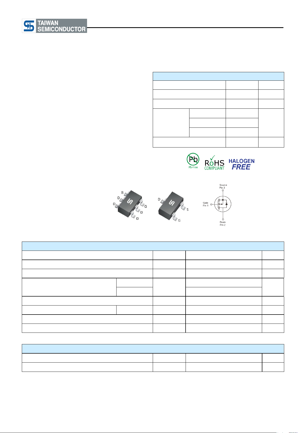
SOT-26
SOT-23
ABSOLUTE MAXIMUM RATINGS (T
A
= 25°C unless otherwise noted)
PARAMETER
SYMBOL
LIMIT
UNIT
Drain-Source Voltage
VDS
-20
V
Gate-Source Voltage
VGS
±10
V
Continuous Drain Current
TC = 25°C
ID
-6.5
A
TC = 100°C
-4.1
Pulsed Drain Current
(Note 1)
IDM
-26
A
Total Power Dissipation
TC = 25°C
P
DTOT
1.56
W
Operating Junction Temperature
TJ
150
ºC
Operating Junction and Storage Temperature Range
TJ, T
STG
- 55 to +150
°C
THERMAL PERFORMANCE
PARAMETER
SYMBOL
LIMIT
UNIT
Junction to Ambient Thermal Resistance
R
ӨJA
80
°C/W
Taiwan Semiconductor
P-Channel Power MOSFET
-20V, -6.5A, 26mΩ
Notes: Moisture sensitivity level: level 3. Per J-STD-020
Notes: R
R
is determined by the user’s board design. R
ӨCA
Document Number: DS_P0000208 1 Version: B15
is the sum of the junction-to-case and case-to-ambient thermal resistances. R
ӨJA
is guaranteed by design while
ӨJA
is shown for single device operation on FR-4 PCB in still air.
ӨJA

TSM260P02
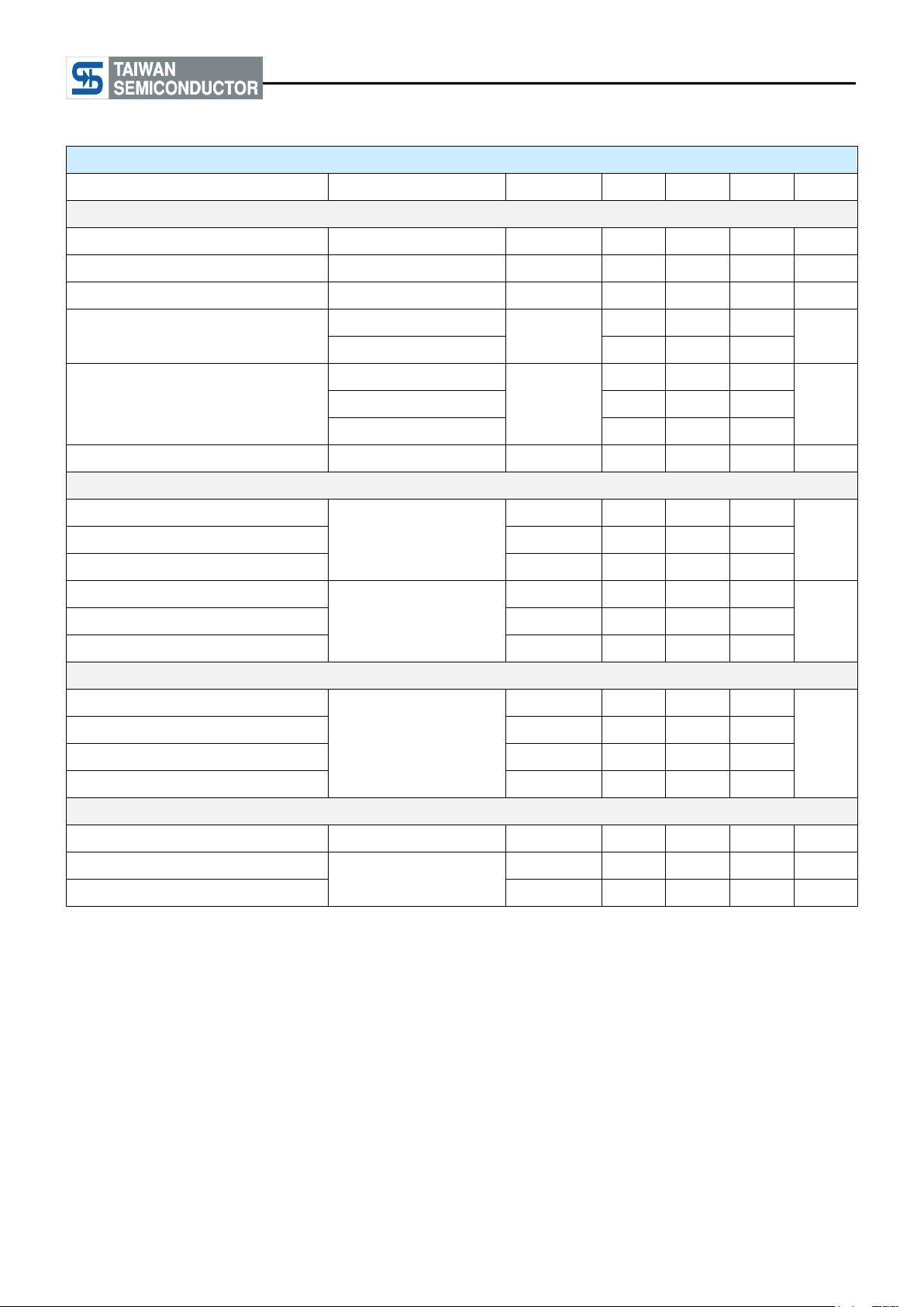
ELECTRICAL SPECIFICATIONS (T
A
= 25°C unless otherwise noted)
PARAMETER
CONDITIONS
SYMBOL
MIN
TYP
MAX
UNIT
Static
(Note 2)
Drain-Source Breakdown Voltage
V
GS
= 0V, ID = -250µA
BV
DSS
-20
--
--
V
Gate Threshold Voltage
V
DS
= VGS, ID = -250µA
V
GS(TH)
-0.3
-0.6
-1.0
V
Gate Body Leakage
VGS = ±10V, VDS = 0V
I
GSS
--
--
±100
nA
Zero Gate Voltage Drain Current
V
DS
= -20V, VGS = 0V
I
DSS
--
--
-1
µA
V
DS
= -16V, TJ = 125ºC
--
--
-10
Drain-Source On-State Resistance
V
GS
= -4.5V, ID = -5A
R
DS(on)
--
21
26
mΩ
V
GS
= -2.5V, ID = -4A
--
26
32
V
GS
= -1.8V, ID = -3A
--
32
40
Forward Transconductance
V
DS
= -10V, IS = -5A
gfs
--
15
--
S
Dynamic
(Note 3)
Total Gate Charge
V
DS
= -10V, ID = -5A,
V
GS
=- 4.5V
Qg
--
19.5
--
nC
Gate-Source Charge
Qgs
-- 2 --
Gate-Drain Charge
Qgd
--
3.6
--
Input Capacitance
V
DS
= -15V, VGS = 0V,
F = 1.0MHz
C
iss
--
1670
--
pF
Output Capacitance
C
oss
--
220
--
Reverse Transfer Capacitance
C
rss
--
120
--
Switching
Turn-On Delay Time
V
DD
= -10V, ID = -1A,
VGS = -4.5V, R
GEN
=25Ω
t
d(on)
--
10.4
--
ns
Turn-On Rise Time
tr
--
37.5
--
Turn-Off Delay Time
t
d(off)
--
89.1
--
Turn-Off Fall Time
tf
--
24.6
--
Source-Drain Diode
Forward Voltage
VGS = 0V, IS = -1A
VSD
--
--
-1
V
Continuous Forward Current
Integral reverse diode
in the MOSFET
IS
--
--
-6.5
A
Pulse Forward Current
ISM
--
--
-26
A
Taiwan Semiconductor
Notes:
1. Pulse width limited by safe operating area
2. Pulse test: PW ≤ 300µs, duty cycle ≤ 2%
3. Switching time is essentially independent of operating temperature.
Document Number: DS_P0000208 2 Version: B15

TSM260P02
PART NO.
PACKAGE
PACKING
TSM260P02CX RFG
SOT-23
3,000pcs / 7” Reel
TSM260P02CX6 RFG
SOT-26
3,000pcs / 7” Reel
ORDERING INFORMATION
Note:
1. Compliant to RoHS Directive 2011/65/EU and in accordance to WEEE 2002/96/EC
2. Halogen-free according to IEC 61249-2-21 definition
Taiwan Semiconductor
Document Number: DS_P0000208 3 Version: B15
 Loading...