

Page 1
T
1
S
3
2
M
~
1
G
~
~
1
1
G
G
C
C
C
T
T
S
S
3
3
2
2
M
M
1. Description
F
F
F
8
8
8
0
0
0
1.1 Feature
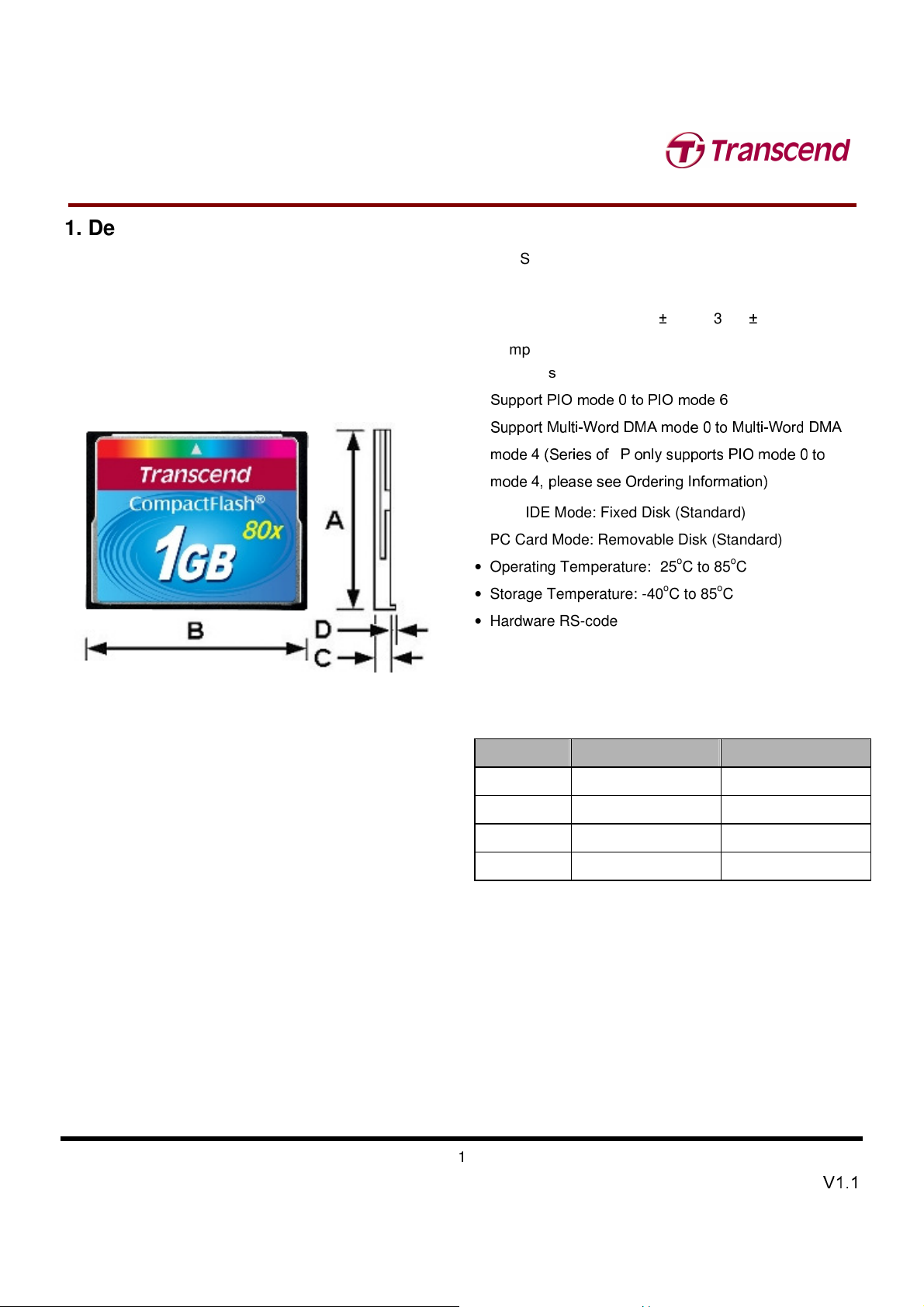
80X CompactFlash Card
The Transcend CF 80X is a High Speed Compact
Flash Card with high quality Flash Memory assembled
on a printed circuit board.
Placement
• RoHS compliant products
• Compliant with CompactFlash® specification V3.0
•
Single Power Supply: 5V ± 10% / 3.3V ± 5%
•
Compliant to CompactFlash, PCMCIA, and ATA
standards
Support PIO mode 0 to PIO mode 6
•
Support Multi-Word DMA mode 0 to Multi-Word DMA
•
mode 4 (Series of –P only supports PIO mode 0 to
mode 4, please see Ordering Information)
•
True IDE Mode: Fixed Disk (Standard)
•
PC Card Mode: Removable Disk (Standard)
•
Operating Temperature: -25oC to 85oC
•
Storage Temperature: -40oC to 85oC
•
Hardware RS-code ECC
•
Support Wear-Leveling to extend product life
•
Durability of Connector: 10,000 times
1.2 Dimensions
Transcend Information Inc.
Side Millimeters Inches
A 36.40 ± 0.150 1.43 ± 0.005
B 42.80 ± 0.100 1.69 ± 0.004
C 3.30 ± 0.100 0.13 ± 0.004
D 0.63 ± 0.070 0.02 ± 0.003
V1.1
Page 2
2
T
T
T
S
S
S
3
3
3
2
2
2
M
M
M
~
~
~
1
1
1
G
G
G
C
C
C
F
F
F
8
8
8
0
0
0
80X CompactFlash Card
1.3 Ordering Information
Part Number Mode Description Transfer mode
CF80
TS32M~1GCF80
TS32M~1GCF80-P
True IDE mode
PCMCIA mode Non-DMA Removable Disk
True IDE mode
PCMCIA mode Non-DMA Removable Disk
DMA Fixed Disk Multiword DMA mode 0~4, PIO mode 0~6
N/A
Non-DMA Fixed Disk PIO mode 0~4
N/A
1.4 CHS and Capacity
Product Name Cylinder Head Sector Capacity
TS32MCF80 62 16 63 29.9MB
TS64MCF80 125 16 63 60.8MB
TS128MCF80 246 16 63 120MB
TS256MCF80 500 16 63 245MB
TS512MCF80 989 16 63 486MB
TS1GCF80 1978 16 63 972MB
Transcend Information Inc.
V1.1
Page 3
T
3
S
3
2
M
~
1
G
T
S
3
2
T
2.Product Specification
M
S
3
2
M
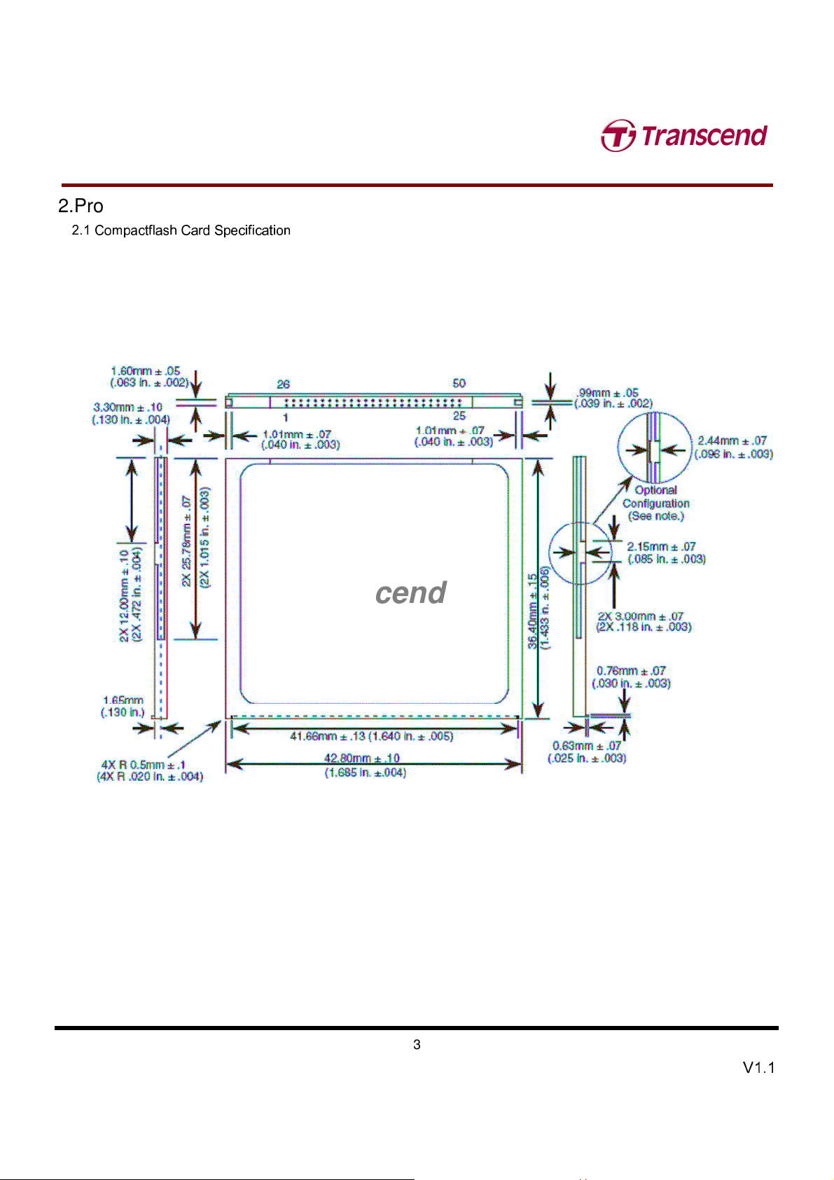
2.1 Compactflash Card Specification
~
~
1
1
G
G
C
C
C
F
F
F
8
8
8
0
0
0
80X CompactFlash Card
Transcend
Transcend Information Inc.
V1.1
Page 4
T
4
S
3
2
M
~
1
G
C
F
8
T
S
3
2
M
~
1
T
S
3
2
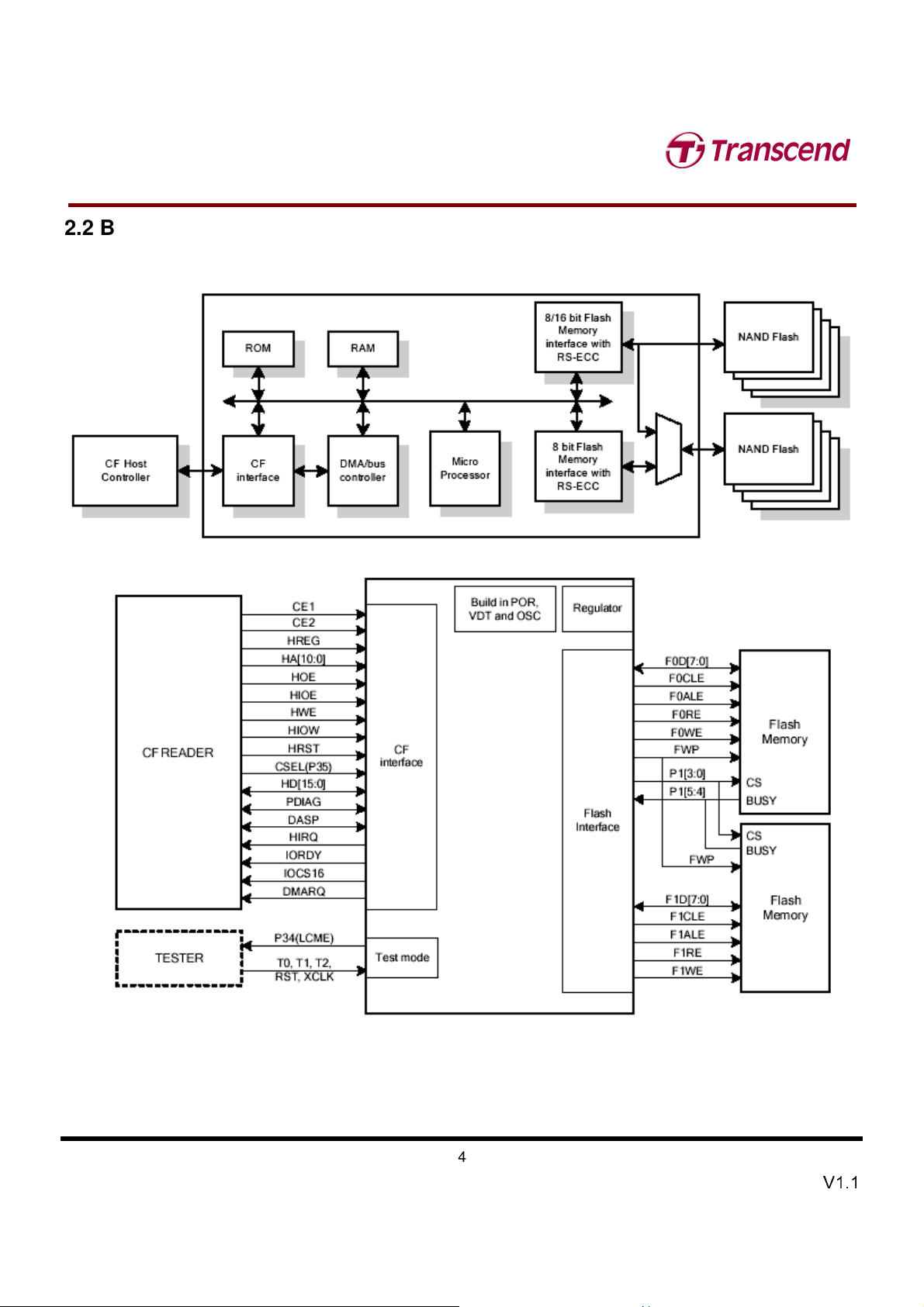
2.2 Block Diagram
M
~
1
G
G
C
C
F
F
8
8
0
0
0
80X CompactFlash Card
Transcend Information Inc.
V1.1
Page 5
5
T
T
T
S
S
S
3
3
3
2
2
2
M
M
M
~
~
~
1
1
1
G
G
G
C
C
C
F
F
F
8
8
8
0
0
0
80X CompactFlash Card
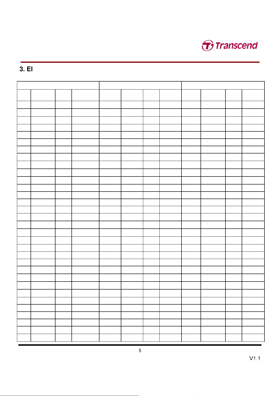
3. Electrical Interface
3.1 Pin Assignment and Pin Type
PC Card Memory Mode
Pin
Num
1 GND
2 D03 I/O I1Z, OZ3 2 D03 I/O I1Z, OZ3
3 D04 I/O I1Z, OZ3 3 D04 I/O I1Z, OZ3
4 D05 I/O I1Z, OZ3 4 D05 I/O I1Z, OZ3
5 D06 I/O I1Z, OZ3 5 D06 I/O I1Z, OZ3
6 D07 I/O I1Z, OZ3 6 D07 I/O I1Z, OZ3
7 -CE1 I I3U 7 -CE1 I I3U 7 -CS0 I I3Z
8 A10 I I1Z 8 A10 I I1Z 8 A102 I I1Z
9 -OE I I3U 9 -OE I I3U 9 -ATA SEL
10
11
12
13
14
15
16
17
18
19
20
21
22
23
24
25
26
27
28
29
30
31
32
Signal
Name
Pin
Type
A09 I I1Z 10 A09 I I1Z 10 A092 I I1Z
A08 I I1Z 11 A08 I I1Z 11 A082 I I1Z
A07 I I1Z 12 A07 I I1Z 12 A072 I I1Z
VCC
A06 I I1Z 14 A06 I I1Z 14 A062 I I1Z
A05 I I1Z 15 A05 I I1Z 15 A052 I I1Z
A04 I I1Z 16 A04 I I1Z 16 A042 I I1Z
A03 I I1Z 17 A03 I I1Z 17 A032 I I1Z
A02 I I1Z 18 A02 I I1Z 18 A02 I I1Z
A01 I I1Z 19 A01 I I1Z 19 A01 I I1Z
A00 I I1Z 20 A00 I I1Z 20 A00 I I1Z
D00 I/O I1Z, OZ3 21 D00 I/O I1Z, OZ3 21 D00 I/O I1Z, OZ3
D01 I/O I1Z, OZ3 22 D01 I/O I1Z, OZ3 22 D01 I/O I1Z, OZ3
D02 I/O I1Z, OZ3 23 D02 I/O I1Z, OZ3 23 D02 I/O I1Z, OZ3
WP O OT3 24 -IOIS16
-CD2 O Ground 25 -CD2 O Ground
-CD1 O Ground 26 -CD1 O Ground
D111 I/O I1Z, OZ3 27 D111 I/O I1Z, OZ3 27 D111 I/O I1Z, OZ3
D121 I/O I1Z, OZ3 28 D121 I/O I1Z, OZ3 28 D121 I/O I1Z, OZ3
D131 I/O I1Z, OZ3 29 D131 I/O I1Z, OZ3 29 D131 I/O I1Z, OZ3
D141 I/O I1Z, OZ3 30 D141 I/O I1Z, OZ3 30 D141 I/O I1Z, OZ3
D151 I/O I1Z, OZ3 31 D151 I/O I1Z, OZ3 31 D151 I/O I1Z, OZ3
-CE21 I I3U 32 -CE21 I I3U 32 -CS11 I I3Z
In, Out Type Pin Num
Ground 1 GND
Power 13 VCC
PC Card I/O Mode
Signal
Name
Pin
Type
O OT3 24 -IOCS16
In, Out
Ground
Power
Type
True IDE Mode
Pin
Num
1 GND
2 D03 I/O I1Z, OZ3
3 D04 I/O I1Z, OZ3
4 D05 I/O I1Z, OZ3
5 D06 I/O I1Z, OZ3
6 D07 I/O I1Z, OZ3
13 VCC
25 -CD2 O Ground
26 -CD1 O Ground
Signal
Name
4
Pin
Type
O ON3
In, Out
Type
Ground
I I3U
Power
Transcend Information Inc.
V1.1
Page 6
T
6
S
T
S
T
S
Pin
Num
3
2
M
~
1
G
C
3
2
M
~
3
1
2
M
~
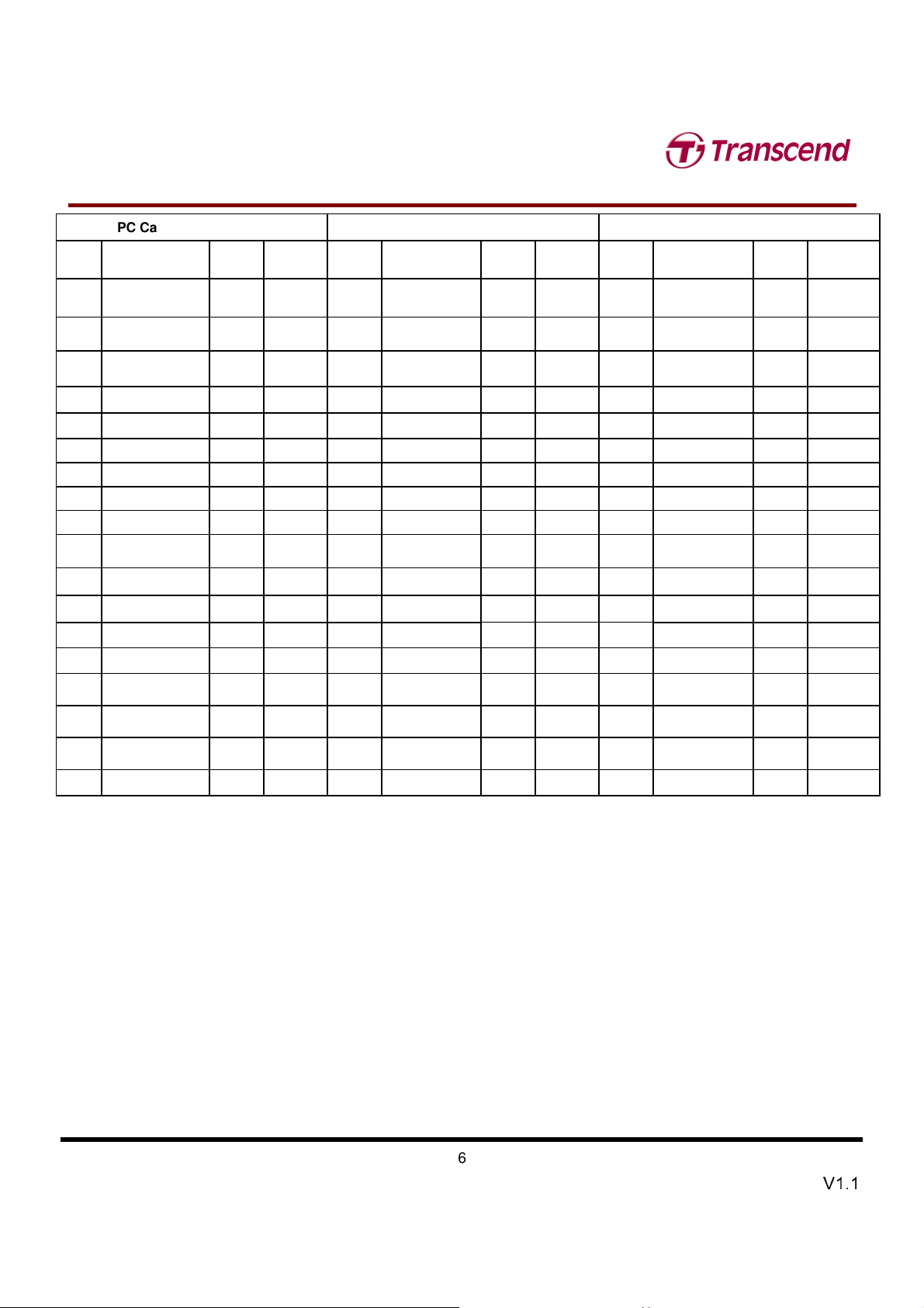
PC Card Memory Mode
Signal Name
1
G
G
C
C
F
F
F
8
0
8
0
8
0
Pin
Type
In, Out
Type
Pin
Num
PC Card I/O Mode
Signal Name
80X CompactFlash Card
Pin
Type
In, Out
Type
Pin
Num
True IDE Mode
Signal Name
4
Pin
Type
In, Out
Type
33
34
35
36
37
38
39
40
41
42
43
44
45
46
47
48
49
50
-VS1 O Ground 33 -VS1 O Ground 33 -VS1 O Ground
-IORD I I3U 34 -IORD I I3U 34 -IORD I I3Z
-IOWR I I3U 35 -IOWR I I3U 35 -IOWR I I3Z
-WE I I3U 36 -WE I I3U 36 -WE3 I I3U
READY O OT1 37 -IREQ O OT1 37 INTRQ O OZ1
VCC Power 38 VCC Power 38 VCC Power
-CSEL5 I I2Z 39 -CSEL5 I I2Z 39 -CSEL I I2U
-VS2 O OPEN 40 -VS2 O OPEN 40 -VS2 O OPEN
RESET I I2Z 41 RESET I I2Z 41 -RESET I I2Z
-WAIT O OT1 42 -WAIT O OT1 42 IORDY O ON1
-INPACK O OT1 43 -INPACK O OT1 43 DMARQ O OZ1
-REG I I3U 44 -REG I I3U 44 -DMACK 6 I I3U
BVD2 O OT1 45 -SPKR O OT1 45 -DASP I/O I1U, ON1
BVD1 O OT1 46 -STSCHG O OT1 46 -PDIAG I/O I1U, ON1
D081 I/O
D091 I/O
D101 I/O
GND Ground 50 GND Ground 50 GND Ground
I1Z,
OZ3
I1Z,
OZ3
I1Z,
OZ3
47 D081 I/O
48 D091 I/O
49 D101 I/O
I1Z,
OZ3
I1Z,
OZ3
I1Z,
OZ3
47 D081 I/O I1Z, OZ3
48 D091 I/O I1Z, OZ3
49 D101 I/O I1Z, OZ3
Note:
1) These signals are required only for 16 bit accesses and not required when installed in 8 bit systems. Devices
should allow for 3-state signals not to consume current.
2) The signal should be grounded by the host.
3) The signal should be tied to VCC by the host.
4) The mode is required for CompactFlash Storage Cards.
5) The -CSEL signal is ignored by the card in PC Card modes. However, because it is not pulled upon the card in these
modes, it should not be left floating by the host in PC Card modes. In these modes, the pin should be connected by the
host to PC Card A25 or grounded by the host.
6) If DMA operations are not used, the signal should be held high or tied to VCC by the host. For proper operation in older
hosts: while DMA operations are not active, the card shall ignore this signal,including a floating condition
Transcend Information Inc.
V1.1
Page 7

T
7
select the following:
ess registers within the CompactFlash Storage Card,
configuration control and status
READY and Write
Present signal in
T
T
S
S
S
3
3
3
2
2
2
M
M
M
~
~
~
1
1
1
G
G
G
C
C
C
F
F
F
8
8
8
0
0
0
3.2 Signal Description
80X CompactFlash Card
Signal Name
A10 – A00
(PC Card Memory Mode)
A10 – A00
(PC Card I/O Mode)
A02 - A00
(True IDE Mode)
BVD1
(PC Card Memory Mode)
-STSCHG
(PC Card I/O Mode)
Status Changed
-PDIAG
(True IDE Mode)
Dir.
I
I
I/O
Pin
8,10,11,12,
14,15,16,17,
18,19,20
18,19,20
46
Description
These address lines along with the -REG signal are used to
The I/O port address registers within the CompactFlash Storage Card , the
memory mapped port addr
a byte in the card's information structure and its
registers.
This signal is the same as the PC Card Memory Mode signal.
In True IDE Mode, only A[02:00] are used to select the one of eight registers
in the Task File, the remaining address lines should be grounded by the
host.
This signal is asserted high, as BVD1 is not supported.
This signal is asserted low to alert the host to changes in the
Protect states, while the I/O interface is configured. Its use is controlled by the
Card Config and Status Register.
In the True IDE Mode, this input / output is the Pass Diagnostic signal in the
Master / Slave handshake protocol.
BVD2
(PC Card Memory Mode)
-SPKR
(PC Card I/O Mode)
-DASP
(True IDE Mode)
I/O
Transcend Information Inc.
45
This signal is asserted high, as BVD2 is not supported.
This line is the Binary Audio output from the card. If the Card does not support
the Binary Audio function, this line should be held negated.
In the True IDE Mode, this input/output is the Disk Active/Slave
the Master/Slave handshake protocol.
V1.1
Page 8
T
8
CompactFlash Storage
indicate to the card
the host to PC
the host to PC
a Master or a
T
T
S
S
S
3
3
3
2
2
2
M
M
M
~
~
~
1
1
1
G
G
G
C
C
C
F
F
F
8
8
8
0
0
0
80X CompactFlash Card
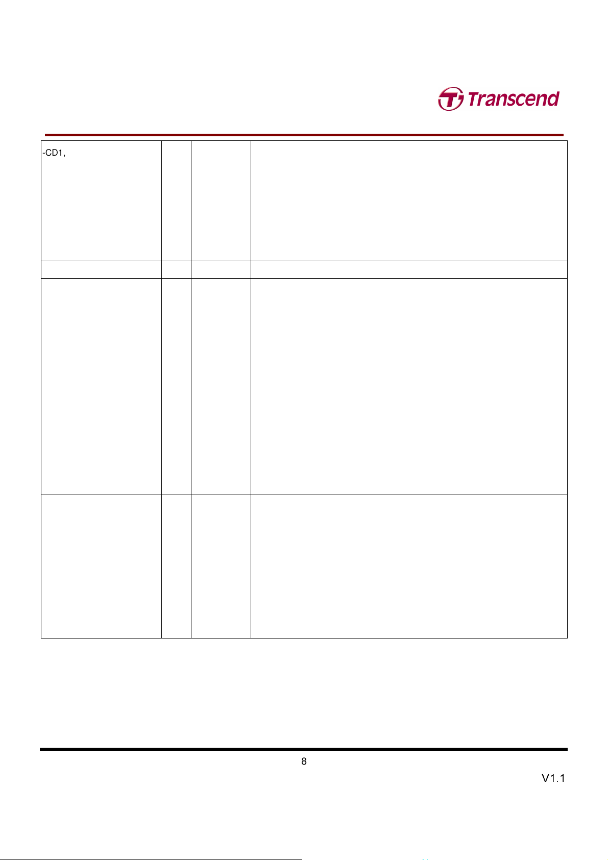
-CD1, -CD2
(PC Card Memory Mode)
-CD1, -CD2
(PC Card I/O Mode)
-CD1, -CD2
(True IDE Mode)
Signal Name
-CE1, -CE2
(PC Card Memory Mode)
Card Enable
-CE1, -CE2
(PC Card I/O Mode)
Card Enable
-CS0, -CS1
(True IDE Mode)
Dir.
O
26,25
Pin
I
7,32
These Card Detect pins are connected to ground on the
Card. They are used by the host to determine that the CompactFlash Storage
Card is fully inserted into its socket.
This signal is the same for all modes.
This signal is the same for all modes.
These input signals are used both to select the card and to
whether a byte or a word operation is being performed. -CE2 always accesses
the odd byte of the word.-CE1 accesses the even byte or the Odd byte of the
word depending on A0 and -CE2. A multiplexing scheme based on A0,-CE1,
-CE2 allows 8 bit hosts to access all data on D0-D7. See Table 27, Table 29,
Table 31, Table 35, Table 36 and Table 37.
This signal is the same as the PC Card Memory Mode signal.
In the True IDE Mode, -CS0 is the address range select for the task file
registers while -CS1 is used to select the Alternate Status Register and the
Device Control Register.
Description
-CSEL
(PC Card Memory Mode)
-CSEL
(PC Card I/O Mode)
-CSEL
(True IDE Mode)
I
Transcend Information Inc.
While –DMACK is asserted, -CS0 and –CS1 shall be held negated and the
width of the transfers shall be 16 bits.
39
This signal is not used for this mode, but should be connected by
Card A25 or grounded by the host.
This signal is not used for this mode, but should be connected by
Card A25 or grounded by the host.
This internally pulled up signal is used to configure this device as
Slave when configured in the True IDE Mode.
When this pin is grounded, this device is configured as a Master.
When the pin is open, this device is configured as a Slave.
V1.1
Page 9
T
9
between the host
Byte of the Word. D08 is the LSB
on the low order
of
transfers between host
device when it is ready to transfer data to
handshake manner with
output signal is not
, the BIOS must report
this does not prevent proper operation in any
S
3
2
M
~
1
G
T
S
3
2
S
3
2
M
M
T
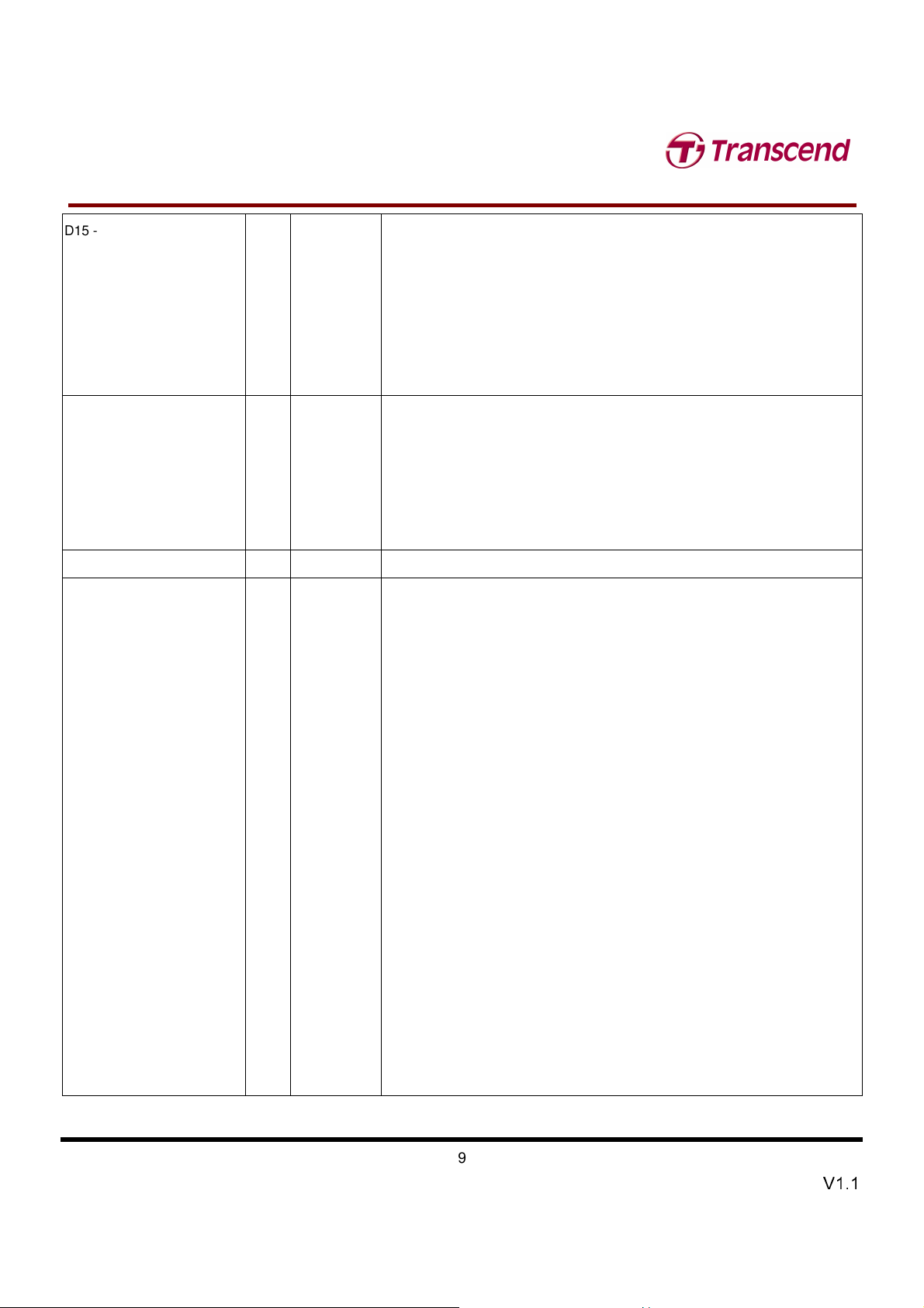
D15 - D00
(PC Card Memory Mode)
D15 - D00
(PC Card I/O Mode)
D15 - D00
(True IDE Mode)
~
~
1
1
C
G
C
G
C
F
F
F
8
0
8
0
8
0
31,30,29,28,
I/O
27,49,48,47,
6,5,4,3,2,
23, 22, 21
These lines carry the Data, Commands and Status information
and the controller. D00 is the LSB of the Even
of the Odd Byte of the Word.
This signal is the same as the PC Card Memory Mode signal.
In True IDE Mode, all Task File operations occur in byte mode
bus D[7:0] while all data transfers are 16 bit using D[15:0].
80X CompactFlash Card
GND
(PC Card Memory Mode)
GND
(PC Card I/O Mode)
GND
(True IDE Mode)
Signal Name
-INPACK
(PC Card Memory Mode)
-INPACK
(PC Card I/O Mode)
Input Acknowledge
DMARQ
(True IDE Mode)
Dir.
--
O
1,50
Pin
43 This signal is not used in this mode.
Ground.
This signal is the same for all modes.
This signal is the same for all modes.
The Input Acknowledge signal is asserted by the CompactFlash Storage Card
when the card is selected and responding to an I/O read cycle at the address
that is on the address bus. This signal is used by the host to control the enable
any input data buffers between the CompactFlash Storage Card and the CPU.
This signal is a DMA Request that is used for DMA data
and device. It shall be asserted by the
or from the host. For Multiword DMA transfers, the direction of data transfer is
controlled by -IORD and -IOWR. This signal is used in a
-DMACK, i.e., the device shall wait until the host asserts -DMACK before
negating DMARQ, and reasserting DMARQ if there is more data to transfer.
Description
Transcend Information Inc.
DMARQ shall not be driven when the device is not selected.
While a DMA operation is in progress, -CS0 and –CS1 shall be held negated
and the width of the transfers shall be 16 bits.
If there is no hardware support for DMA mode in the host, this
used and should not be connected at the host. In this case
that DMA mode is not supported by the host so that device drivers will not
attempt DMA mode.
A host that does not support DMA mode and implements both PCMCIA and
True-IDE modes of operation need not alter the PCMCIA mode connections
while in True-IDE mode as long as
mode.
V1.1
Page 10
T
10
gates I/O data onto
Card when the card is configured to use
operation and is held low when the card is
shall not cause the READY signal to remain continuously in
Interrupt Request. This line is
S
3
2
M
~
1
G
C
T
S
3
2
M
~
2
M
~
1
T
S
3
-IORD
(PC Card Memory Mode)
-IORD
(PC Card I/O Mode)
-IORD
(True IDE Mode )
-IOWR
(PC Card Memory Mode)
-IOWR
(PC Card I/O Mode)
-IOWR
(True IDE Mode)
Signal Name
F
G
C
1
F
G
C
Dir.
F
8
8
8
0
0
0
I
I
34 This signal is not used in this mode.
This is an I/O Read strobe generated by the host. This signal
the bus from the CompactFlash Storage
the I/O interface.
In True IDE Mode, this signal has the same function as in PC Card I/O Mode.
35
Pin
This signal is not used in this mode.
The I/O Write strobe pulse is used to clock I/O data on the Card Data bus into
the CompactFlash Storage Card controller registers when the CompactFlash
Storage Card is configured to use the I/O interface.
The clocking shall occur on the negative to positive edge of the signal (trailing
edge).
In True IDE Mode, this signal has the same function as in PC Card I/O Mode.
80X CompactFlash Card
Description
-OE
(PC Card Memory Mode)
-OE
(PC Card I/O Mode)
-ATA SEL
(True IDE Mode)
READY
(PC Card Memory Mode)
-IREQ
(PC Card I/O Mode)
INTRQ
(True IDE Mode)
I
O
9
37
This is an Output Enable strobe generated by the host interface. It is used to
read data from the CompactFlash Storage Card in Memory Mode and to read
the CIS and configuration registers.
In PC Card I/O Mode, this signal is used to read the CIS and configuration
registers.
To enable True IDE Mode this input should be grounded by the host.
In Memory Mode, this signal is set high when the CompactFlash Storage Card
is ready to accept a new data transfer
busy.
At power up and at Reset, the READY signal is held low (busy) until the
CompactFlash Storage Card has completed its power up or reset function. No
access of any type should be made to the CompactFlash Storage Card during
this time.
Note, however, that when a card is powered up and used with RESET
continuously disconnected or asserted, the Reset function of the RESET pin is
disabled. Consequently, the continuous assertion of RESET from the
application of power
the busy state.
I/O Operation – After the CompactFlash Storage Card Card has been
configured for I/O operation, this signal is used as strobed low to generate a pulse mode interrupt or held low for a level mode
interrupt.
In True IDE Mode signal is the active high Interrupt Request to the host.
Transcend Information Inc.
V1.1
Page 11

T
11
High for Common Memory,
DMACK signal,
RESET pin is high with the
S
3
2
M
~
1
G
C
T
S
3
2
M
~
2
M
~
1
T
S
3
-REG
(PC Card Memory Mode)
Attribute Memory Select
-REG
(PC Card I/O Mode)
1
G
G
F
C
F
C
F
8
8
8
0
0
0
I
44
This signal is used during Memory Cycles to distinguish between Common
Memory and Register (Attribute) Memory accesses.
Low for Attribute Memory.
The signal shall also be active (low) during I/O Cycles when the I/O address is
on the Bus.
80X CompactFlash Card
-DMACK
(True IDE Mode)
Signal Name
RESET
(PC Card Memory Mode)
RESET
(PC Card I/O Mode)
-RESET
(True IDE Mode)
Dir.
I
This is a DMA Acknowledge signal that is asserted by the host in response to
DMARQ to initiate DMA transfers.
While DMA operations are not active, the card shall ignore the including a floating condition.
If DMA operation is not supported by a True IDE Mode only host, this signal
should be driven high or connected to VCC by the host.
A host that does not support DMA mode and implements both PCMCIA and
True-IDE modes of operation need not alter the PCMCIA mode connections
while in True-IDE mode as long as this does not prevent proper operation all
modes.
Pin
41 The CompactFlash Storage Card is Reset when the
following important exception:
The host may leave the RESET pin open or keep it continually high from the
application of power without causing a continuous Reset of the card. Under
either of these conditions, the card shall emerge from power-up having
completed an initial Reset.
The CompactFlash Storage Card is also Reset when the Soft Reset bit in the
Card Configuration Option Register is set.
This signal is the same as the PC Card Memory Mode signal.
In the True IDE Mode, this input pin is the active low hardware reset from the
host.
Description
VCC
(PC Card Memory Mode)
VCC
(PC Card I/O Mode)
VCC
(True IDE Mode)
Transcend Information Inc.
--
13,38 +5 V, +3.3 V power.
This signal is the same for all modes.
This signal is the same for all modes.
V1.1
Page 12
T
12
VS2 is
Card to signal the
write data to the
registers of the CompactFlash Storage Card when the card is configured in the
connected to VCC
does not have a write protect
IOIS16) function. A
that a 16 bit or odd byte only operation can be performed at
device is expecting
T
T
S
S
S
3
3
3
2
2
2
M
M
M
~
~
~
1
1
1
G
G
G
C
C
C
F
F
F
8
8
8
0
0
0
80X CompactFlash Card
-VS1
-VS2
(PC Card Memory Mode)
-VS1
-VS2
(PC Card I/O Mode)
-VS1
-VS2
(True IDE Mode)
-WAIT
(PC Card Memory Mode)
-WAIT
(PC Card I/O Mode)
IORDY
(True IDE Mode)
Signal Name
-WE
(PC Card Memory Mode)
-WE
(PC Card I/O Mode)
-WE
(True IDE Mode)
WP
(PC Card Memory Mode)
Write Protect
-IOIS16
(PC Card I/O Mode)
-IOCS16
(True IDE Mode)
Dir.
O
O
I
O
33
40
42 The -WAIT signal is driven low by the CompactFlash Storage
Pin
36 This is a signal driven by the host and used for strobing memory
24
Voltage Sense Signals. -VS1 is grounded on the Card and sensed by the Host
so that the CompactFlash Storage Card CIS can be read at 3.3 volts and reserved by PCMCIA for a secondary voltage and is not connected on the Card.
This signal is the same for all modes.
This signal is the same for all modes.
host to delay completion of a memory or I/O cycle that is in progress.
This signal is the same as the PC Card Memory Mode signal.
In True IDE Mode, except in Ultra DMA modes, this output signal may be used
as IORDY.
memory interface mode. It is also used for writing the configuration registers.
In PC Card I/O Mode, this signal is used for writing the configuration registers.
In True IDE Mode, this input signal is not used and should be
by the host.
Memory Mode – The CompactFlash Storage Card
switch. This signal is held low after the completion of the reset initialization
sequence.
I/O Operation – When the CompactFlash Storage Card is configured for I/O
Operation Pin 24 is used for the -I/O Selected is 16 Bit Port (Low signal indicates
the addressed port.
In True IDE Mode this output signal is asserted low when this
a word data transfer cycle.
Description
Transcend Information Inc.
V1.1
Page 13
T
13
T
T
S
S
S
3
3
3
2
2
2
M
M
M
~
~
~
1
1
1
G
G
G
C
C
C
F
F
F
8
8
8
0
0
0
80X CompactFlash Card
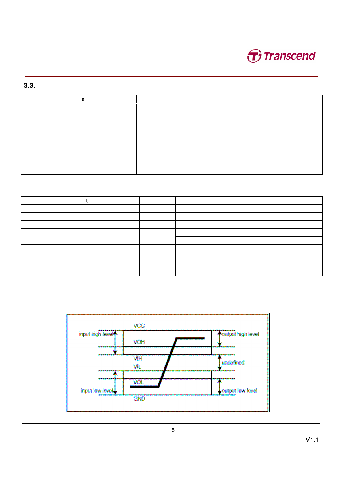
3.3 Electrical Specification
The following tables indicate all D.C. Characteristics for the CompactFlash Storage Card. Unless otherwise stated,
conditions are:
Vcc = 5V ±10%
Vcc = 3.3V ± 5%
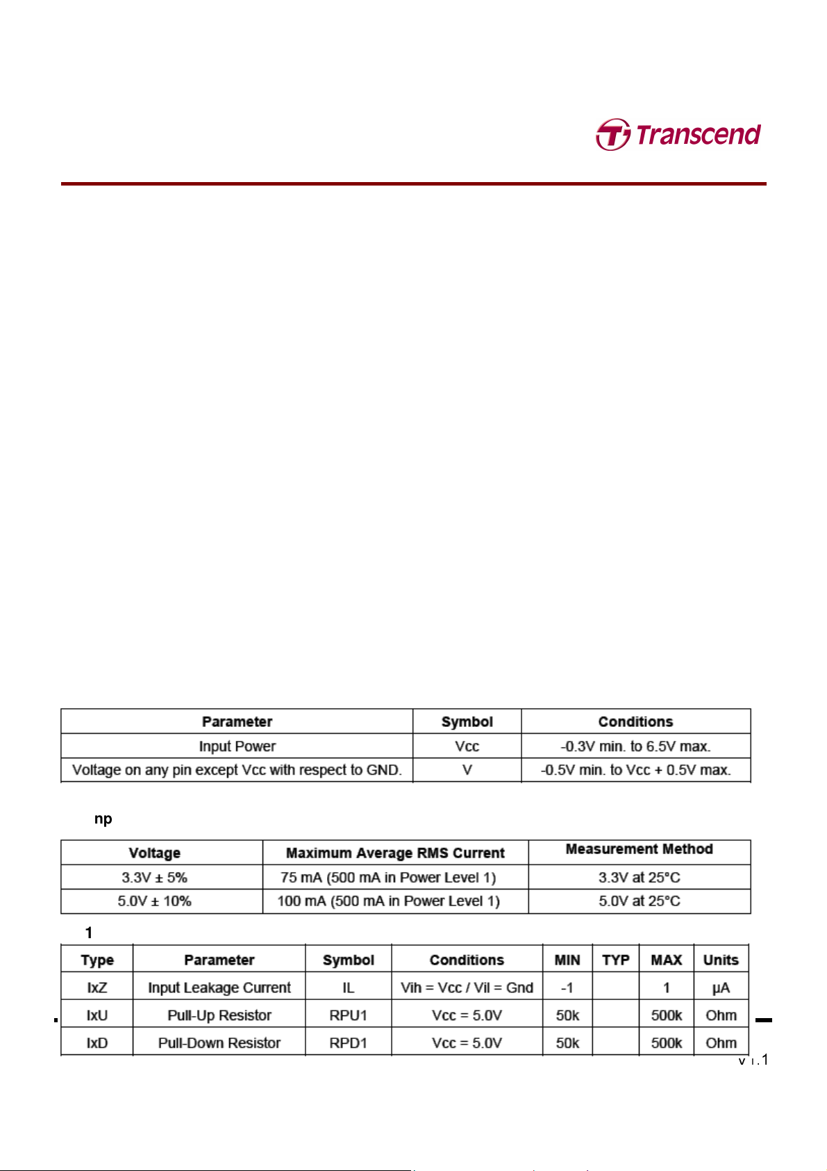
Absolute Maximum Conditions
Input Power
3.3.1 Input Leakage Current
Transcend Information Inc.
V1.1
Page 14
T
14
T
T
S
S
S
3
3
3
2
2
2
M
M
M
~
~
~
1
1
1
G
G
G
C
C
C
F
F
F
8
8
8
0
0
0
80X CompactFlash Card
3.3.2 Input Characteristics
3.3.2.1 CompactFlash interface I/O at 5.0V
Parameter Symbol Min. Max. Unit Remark
Supply Voltage VCC 4.5 5.5 V
High level output voltage VOH VCC-0.8
Low level output voltage VOL 0.8 V
High level input voltage VIH
Low level input voltage VIL
Pull up resistance2 RPU 52.54 86.56 kOhm
Pull down resistance RPD 63 244 kOhm
V
4.0 V Non-schmitt trigger
2.6 V Schmitt trigger1
0.8 V Non-schmitt trigger
1.79 V Schmitt trigger1
Transcend Information Inc.
V1.1
Page 15
T
15
T
T
S
S
S
3
3
3
2
2
2
M
M
M
~
~
~
1
1
1
G
G
G
C
C
C
F
F
F
8
8
8
0
0
0
80X CompactFlash Card
3.3.2.2 CompactFlash interface I/O at 3.3V
Parameter Symbol Min. Max. Unit Remark
Supply Voltage VCC 3.135 3.465 V
High level output voltage VOH VCC-0.8
Low level output voltage VOL 0.8 V
High level input voltage VIH
Low level input voltage VIL
Pull up resistance2 RPU 81.39 154.85 kOhm
Pull down resistance RPD 42 172 kOhm
3.3.2.3 The I/O pins other than CompactFlash interface
Parameter Symbol Min. Max. Unit Remark
Supply Voltage VCC 3.135 3.465
High level output voltage VOH 2.4 V
Low level output voltage VOL 0.4 V
High level input voltage VIH
Low level input voltage VIL
Pull up resistance RPU 40 kOhm
Pull down resistance RPD 40 kOhm
1. Include CE1,CE2 ,HREG ,HOE ,HIOE ,HWE ,HIOW pins.
V
2.4 V Non-schmitt trigger
1.67 V Schmitt trigger1
0.6 V Non-schmitt trigger
1.07 V Schmitt trigger1
V
2.0 V Non-schmitt trigger
1.4 V Schmitt trigger
0.8 V Non-schmitt trigger
1.2 V Schmitt trigger
2. Include CE1,CE2 ,HREG ,HOE , HIOE ,HWE ,HIOW ,CSEL ,PDIAG ,DASP pins.
Transcend Information Inc.
V1.1
Page 16
T
16
T
T
S
S
S
3
3
3
2
2
2
M
M
M
~
~
~
1
1
1
G
G
G
C
C
C
F
F
F
8
8
8
0
0
0
80X CompactFlash Card
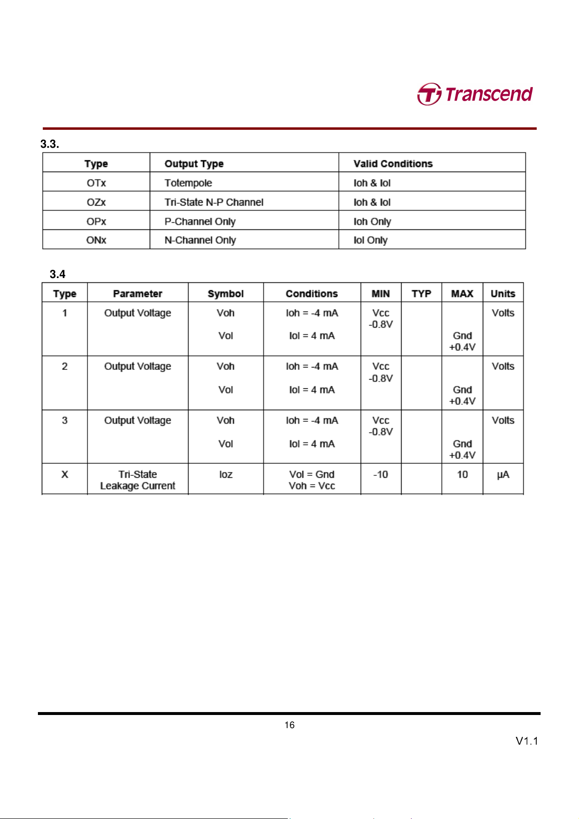
3.3.3 Output Drive Type
3.3.4 Output Drive Characteristics
Transcend Information Inc.
V1.1
Page 17
T
17
Gnd R
up
S
3
2
M
~
1
G
C
F
C
C
F
F
8
8
T
T
S
S
3
3
2
2
M
M
~
~
1
1
G
G
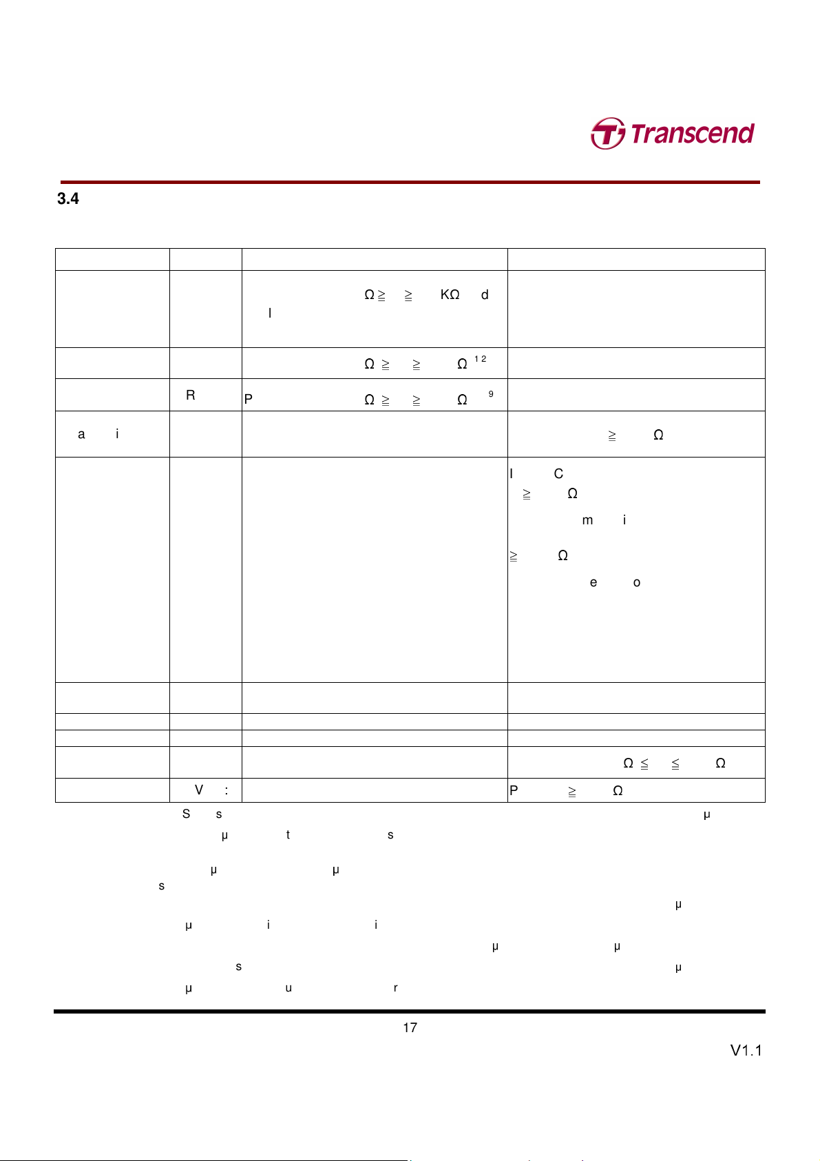
3.4 Signal Interface
8
0
0
0
80X CompactFlash Card
Electrical specifications shall be maintained to ensure data reliability.
Item Signal Card10 Host
-CE1
-CE2
Control Signal
RESET
Status Signal
-INPACK
-REG
-IORD
-IOWR
-OE
-WE
READY
-WAIT
WP
Pull-up to VCC 500 K
shall be sufficient to keep inputs inactive
when the pins are not connected at the host.
Pull-up to VCC 500 KΩ ≧ R ≧ 50 KΩ.
Pull-up to VCC 500 KΩ ≧ R ≧ 50 KΩ.
Ω ≧ R≧
50 KΩ and
1
1,2
1,2,9,
Pull-up to VCC R ≧ 10 KΩ.
In PCMCIA PC Card modes Pull-up to V
R ≧ 10 KΩ.4
In True IDE mode, if DMA operation is
supported by the host, Pull-down to
≧
5.6 KΩ.5
PC Card / True IDE hosts switch the pullto pull down in True IDE mode if DMA
operation is supported.
The PC Card mode Pull-up may be left
active during True IDE mode if True IDE
DMA operation is not supported.
10
3
CC
Address
Data Bus D[15:00]
Card Detect
Voltage Sense
Battery/Detect BVD[2:1]
Notes: 1) Control Signals: each card shall present a load to the socket no larger than 50 pF
2) Resistor is optional.
3) Status Signals: the socket shall present a load to the card no larger than 50 pF
and 100 μA high state, including pull-up resistor. The card shall be able to drive at least the following load
meeting all AC timing requirements: 50 pF at a DC current of 400 μA low state and 100 μA high state.
4) Status Signals: the socket shall present a load to the card no larger than 50 pF
and 100 μA high state, including pull-up resistor. The card shall be able to drive at least the following load
Transcend Information Inc.
A[10:00]
-CSEL
-CD[2:1] Connected to GND in the card
-VS1
-VS2
state and 150 μA high state, including pull-resistor. The socket shall be able to drive at least the following load
while meeting all AC timing requirements: (the number of sockets wired in parallel) multiplied by (50 pF with DC
current 700 μA low state and 150 μA high state per socket).
1.
Pull-up to Vcc 10 KΩ ≦ R ≦100KΩ.
Pull-up R ≧ 50 KΩ.
10
at a DC current of 700 μA low
10
at a DC current of 400 μA low state
10
at a DC current of 400 μA low state
3.6
10
while
10
while
10
V1.1
Page 18
T
18
T
T
S
S
S
3
2
M
~
1
G
3
2
M
3
2
M
5) Status Signals: the socket shall present a load to the card no larger than 50 pF
6) BVD2 was not defined in the JEIDA 3.0 release. Systems fully supporting JEIDA release 3 SRAM cards shall pull-up
7) Address Signals: each card shall present a load of no more than 100pF
8) Data Signals: the host and each card shall present a load no larger than 50pF
9) Reset Signal: This signal is pulled up to prevent the input from floating when a CFA to PCMCIA adapter is used in a
C
~
1
G
C
~
1
G
C
meeting all AC timing requirements: 50 pF at a DC current of 400 μA low state and 100 μA high state.
and 100 μA high state, including pull-up resistor. The card shall be able to drive at least the following load
meeting all AC timing requirements: 50 pF at a DC current of 400 μA low state and 1100 μA high state.
pin 45 (BVD2) to avoid sensing their batteries as “Low.”
150μA high state. The host shall be able to drive at least the following load
requirements: (the number of sockets wired in parallel) multiplied by (100pF with DC current 450μA low state and
150μA high state per socket).
μ
A high state. The host and each card shall be able to drive at least the following load
timing requirements: 100pF with DC current 1.6mA low state and 300μA high state. This permits the host to wire
two sockets in parallel without derating the card access speeds.
PCMCIA revision 1 host. However, to minimize DC current drain through the pull-up resistor in normal operation the
pull-up should be turned off once the Reset signal has been actively driven low by the host. Consequently, the input
is specified as an I2Z because the resistor is not necessarily detectable in the input current leakage test.
F
F
F
8
8
8
0
0
0
80X CompactFlash Card
10
at a DC current of 400 μA low state
10
at a DC current of 450μA low state and
10
while meeting all AC timing
10
at a DC current of 450μA and 150
10
while meeting all AC
10
while
Transcend Information Inc.
V1.1
Page 19
T
19
S
3
2
M
~
1
G
T
S
3
2
S
3
2
M
M
T
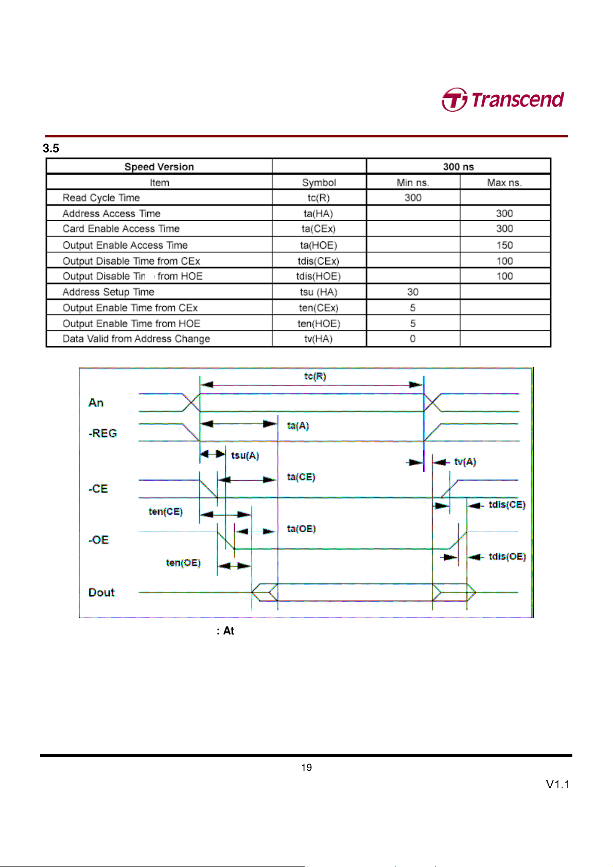
3.5 Attribute Memory Read Timing
~
~
1
1
G
G
C
C
C
F
F
F
8
8
8
0
0
0
80X CompactFlash Card
Transcend Information Inc.
Figure: Attribute Memory Read Timing Diagram
V1.1
Page 20
20
T
S
3
2
M
~
1
G
T
S
3
2
S
3
2
M
M
T
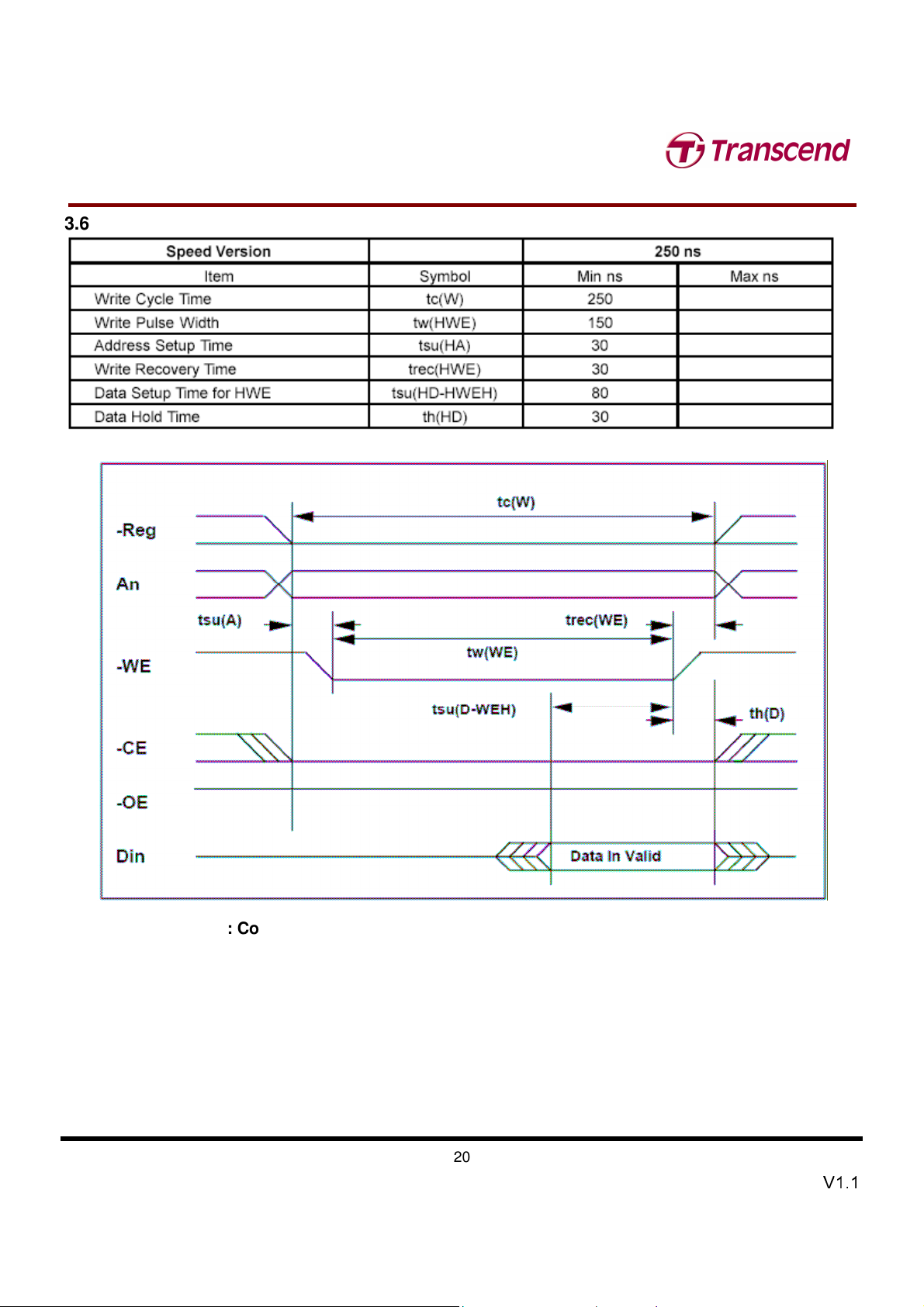
3.6 Configuration Register (Attribute Memory) Write Timing
~
~
1
1
G
G
C
C
C
F
F
F
8
8
8
0
0
0
80X CompactFlash Card
Figure: Configuration Register (Attribute Memory) Write Timing Diagram
Transcend Information Inc.
V1.1
Page 21
T
21
T
T
S
S
S
3
3
3
2
2
2
M
M
M
~
~
~
1
1
1
G
G
G
C
C
C
F
F
F
8
8
8
0
0
0
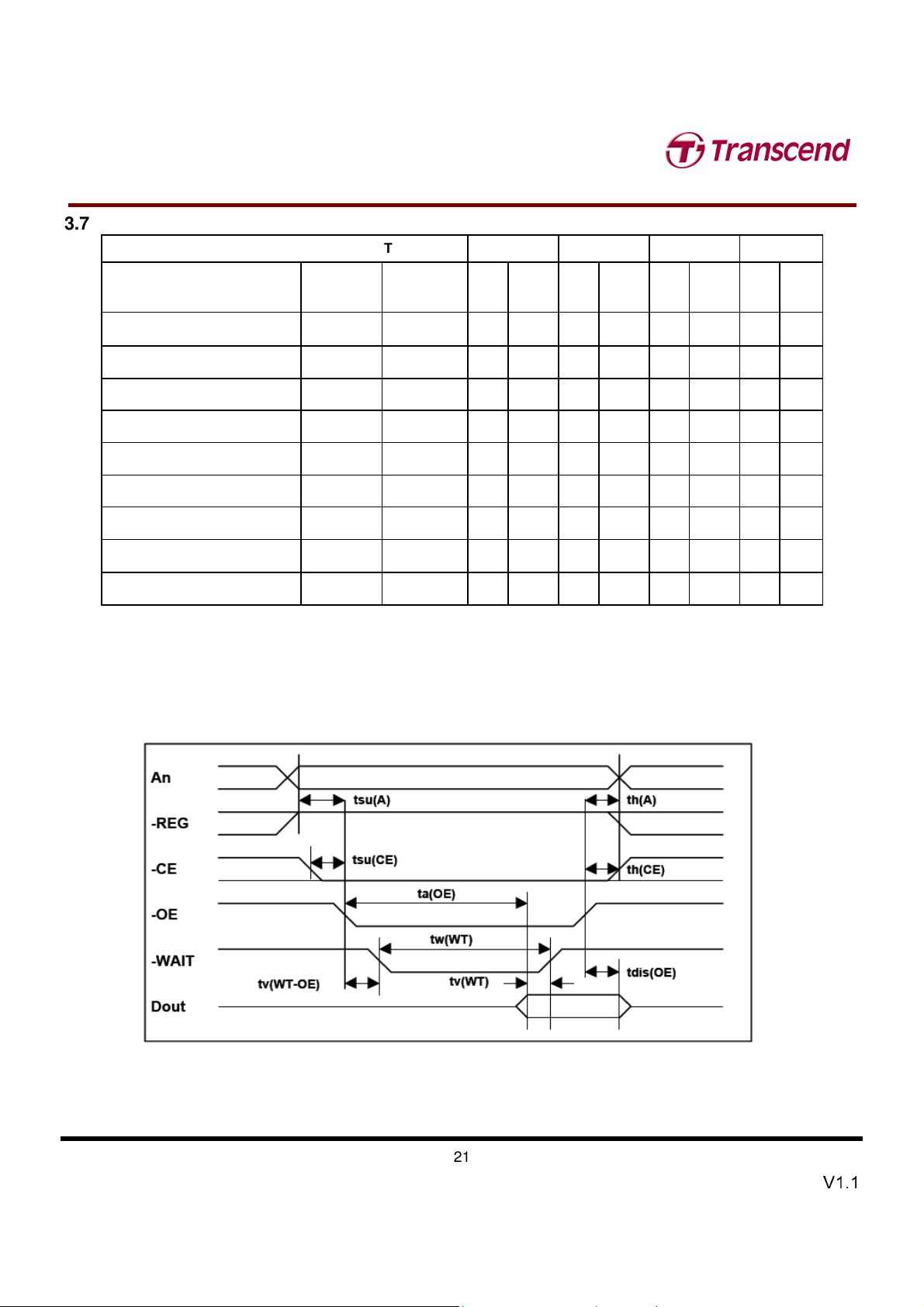
3.7 Common Memory Read Timing Specification
Cycle Time Mode:
Item
Output Enable Access Time ta(OE) tGLQV
Symbol
IEEE
Symbol
Min
ns.
250 ns
Max
125
ns.
120 ns
Min
ns.
80X CompactFlash Card
Max
ns.
60
100 ns
Min
ns.
Max
ns.
50
80 ns
Min
ns.
Ma
x
ns.
45
Output Disable Time from OE tdis(OE) tGHQZ
Address Setup Time tsu(A) tAVGL 30
Address Hold Time th(A) tGHAX 20
CE Setup before OE tsu(CE) tELGL 0
CE Hold following OE th(CE) tGHEH 20
Wait Delay Falling from OE
Data Setup for Wait Release tv(WT) tQVWTH
Wait W idth Time
Notes:1) –WAIT is not supported in this mode.
2) The maximum load on -WAIT is 1 LSTTL with 50 pF (40pF below 120nsec Cycle Time) total load. All times are in
nanoseconds. Dout signifies data provided by the CompactFlash Storage Card to the system. The -WAIT signal may be ignored
if the -OE cycle to cycle time is greater than the W ait Width time. The Max Wait Width time can be determined from the Card
Information Structure. The W ait Width time meets the PCMCIA PC Card specification of 12µs but is intentionally less in this
specification.
2
tv(WT-OE
)
tw(WT) tWTLWTH
tGLWTV
100
35
0
350
15
15
0
15
60
35
0
350
10
15
0
15
50
35
0
350
10
10
0
10
45
na
na
na
1
1
1
Transcend Information Inc.
V1.1
Page 22
T
22
T
T
S
S
S
3
3
3
2
2
2
M
M
M
~
~
~
1
1
1
G
G
G
C
C
C
F
F
F
8
8
8
0
0
0
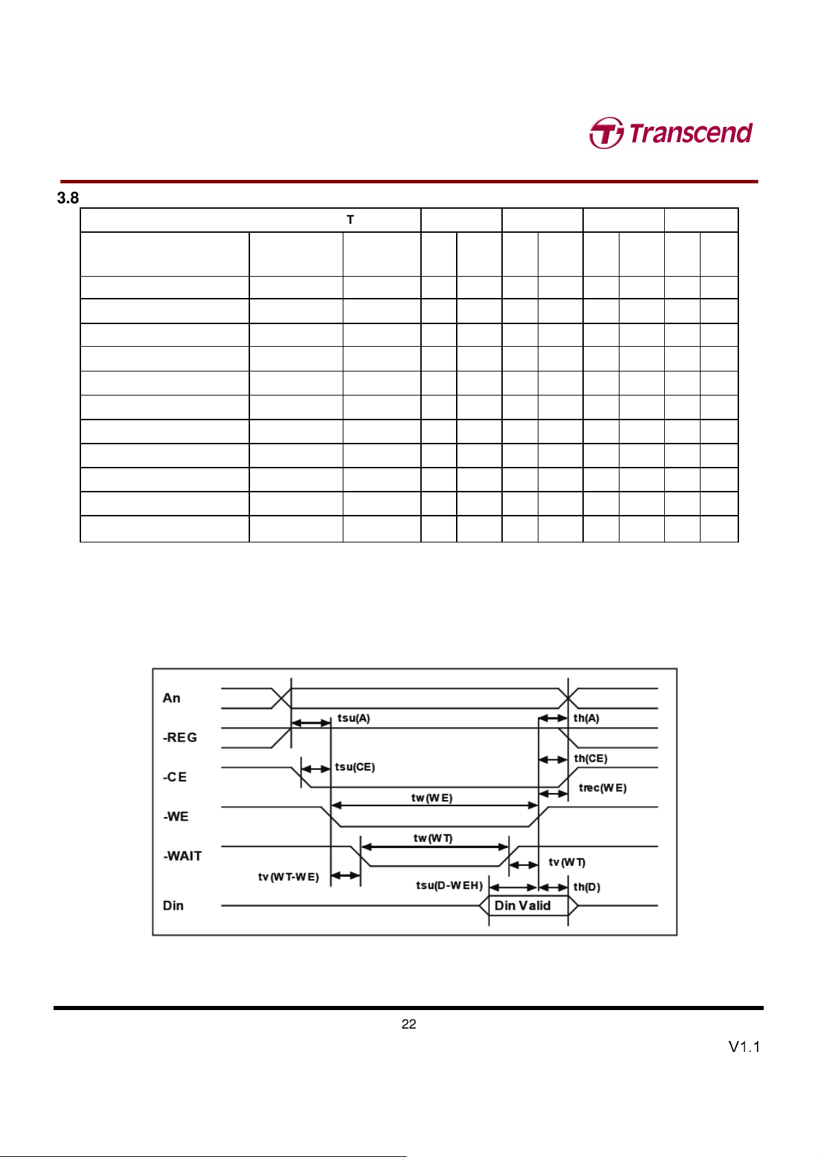
3.8 Common Memory Write Timing Specification
Cycle Time Mode: 250 ns
Item
Data Setup before WE tsu (D-WEH) tDVWH 80
Data Hold following WE th(D) tWMDX 30
WE Pulse Width tw(WE) tWLWH 150
Address Setup Time tsu(A) tAVWL 30
Symbol
IEEE
Symbol
Min
Max
ns.
ns.
Min
ns.
50
15
70
15
80X CompactFlash Card
120 ns
Max
ns.
100 ns
Min
Max
ns.
ns.
40
10
60
10
80 ns
Ma
Min
x
ns.
ns.
30
10
55
10
CE Setup before WE tsu(CE) tELWL 0
Write Recovery Time trec(WE) tWMAX 30
Address Hold Time th(A) tGHAX 20
CE Hold following WE th(CE) tGHEH 20
Wait Delay Falling from WE tv (WT-WE) tWLWTV
WE High from Wait Release tv(WT) tWTHWH 0
Wait Width Time
Notes: 1) –WAIT is not supported in this mode.
2) The maximum load on -WAIT is 1 LSTTL with 50 pF (40pF below 120nsec Cycle Time) total load. All times are in
nanoseconds. Din signifies data provided by the system to the CompactFlash Storage Card. The -W AIT signal may be
ignored if the -WE cycle to cycle time is greater than the Wait Width time. The Max Wait Width time can be determined from
the Card Information Structure. The Wait Width time meets the PCMCIA PC Card specification of 12µs but is intentionally
less in this specification.
2
tw (WT) tWTLWTH
35
350
0
15
15
15
35
0
350
0
15
15
15
0
35
350
15
15
10
na
0
1
na
1
1
na
Transcend Information Inc.
V1.1
Page 23
23
T
S
3
2
M
~
1
G
~
~
1
1
G
G
C
C
C
T
T
S
S
3
3
2
2
M
M
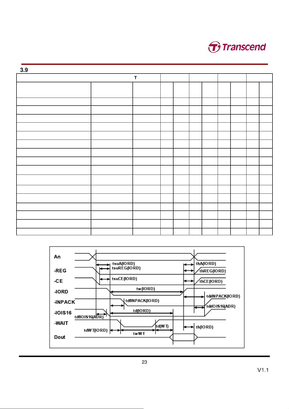
3.9 I/O Input (Read) Timing Specification
Item
Data Delay after IORD td(IORD) tlGLQV
Data Hold following IORD th(IORD) tlGHQX 0
IORD Width Time tw(IORD) tlGLIGH 165
Address Setup before IORD tsuA(IORD) tAVIGL 70
F
F
F
8
8
8
0
0
0
Cycle Time Mode: 250 ns
Symbol
IEEE
Symbol
Min
ns.
80X CompactFlash Card
Max
ns.
100
120 ns
Min
Max
ns.
5
70
25
ns.
50
100 ns
Min
Max
ns.
5
65
25
ns.
50
80 ns
Min
ns.
55
15
Ma
x
ns.
45
5
Address Hold following IORD thA(IORD) tlGHAX 20
CE Setup before IORD tsuCE(IORD) tELIGL 5
CE Hold following IORD thCE(IORD) tlGHEH 20
REG Setup before IORD tsuREG (IORD) tRGLIGL 5
REG Hold following IORD thREG (IORD) tlGHRGH 0
INPACK Delay Falling from IORD3 tdfINPACK (IORD) tlGLIAL 0 45 0 na1 0 na1 0 na
INPACK Delay Rising from IORD3 tdrINPACK (IORD) tlGHIAH
IOIS16 Delay Falling from Address
IOIS16 Delay Rising from Address
Wait Delay Falling from IORD3 tdWT(IORD) tlGLWTL
Data Delay from Wait Rising3 td(WT) tWTHQV
Wait W idth Time3 tw(WT) tWTLWTH
3
tdfIOIS16 (ADR) tAVISL
3
tdrIOIS16 (ADR) tAVISH
350
45
35
35
35
0
10
5
10
5
0
na1 na1 na
na1 na1 na
na1 na1 na
350
10
5
10
5
0
35 35 na
0 0 na
350
10
5
10
5
0
na
1
1
1
1
2
2
2
Transcend Information Inc.
V1.1
Page 24
24
T
S
3
2
M
~
1
G
~
~
1
1
G
G
C
C
C
T
T
S
S
3
3
2
2
M
M
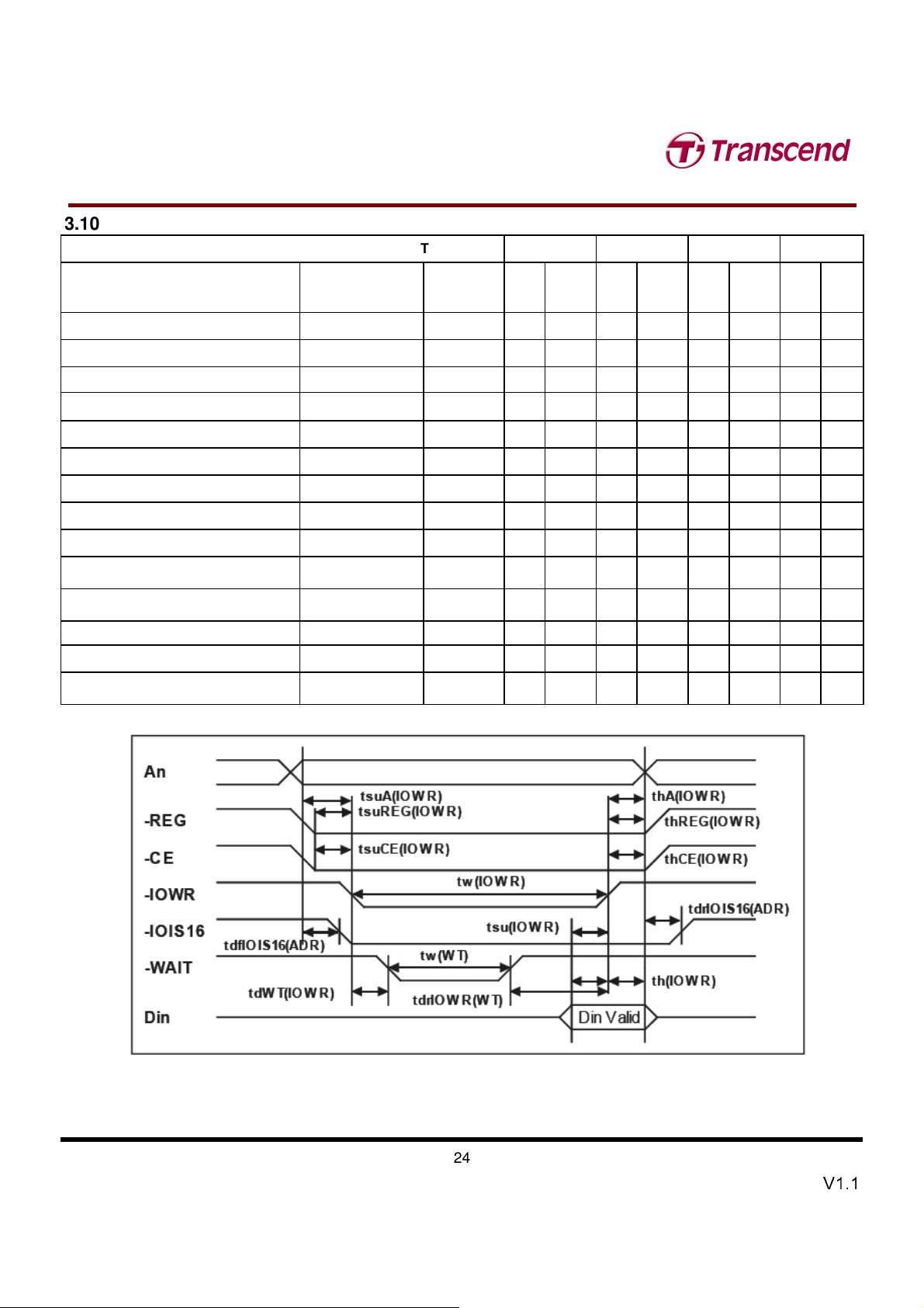
3.10 I/O Output (Write) Timing Specification
Item
Data Setup before IOWR tsu(IOWR) tDVIWH 60
F
F
F
8
8
8
0
0
0
Cycle Time Mode: 255 ns
Symbol
IEEE
Symbol
Min
ns.
80X CompactFlash Card
Min
ns.
120 ns
Max
ns.
Max
ns.
20 20 15
100 ns
Min
Max
ns.
ns.
Min
ns.
80 ns
Ma
x
ns.
Data Hold following IOWR th(IOWR) tlWHDX 30
IOWR Width Time tw(IOWR) tlWLIWH 165 70 65 55
Address Setup before IOW R tsuA(IOWR) tAVIWL 70
Address Hold following IOW R thA(IOWR) tlWHAX 20
CE Setup before IOWR tsuCE (IOWR) tELIW L 5
CE Hold following IOWR thCE (IOW R) tlWHEH 20
REG Setup before IOWR tsuREG (IOWR) tRGLIWL 5
REG Hold following IOWR thREG (IOWR) tlWHRGH 0
IOIS16 Delay Falling from Address3 tdfIOIS16 (ADR) tAVISL 35
IOIS16 Delay Rising from Address3 tdrIOIS16 (ADR) tAVISH 35
Wait Delay Falling from IOWR3 tdWT(IOWR) tlWLWTL
IOWR high from Wait high3 tdrIOWR (W T) tWTJIWH 0
Wait W idth Time3 tw(WT)
tWTLWT
H
35
350 350
10 5 5
25 25 15
20 10 10
5 5 5
20 10 10
5 5 5
0 0 0
na1 na1
na1 na1
35 35 na2
0 0 na2
350
na2
na1
na1
Transcend Information Inc.
V1.1
Page 25
25
T
S
3
2
M
~
1
G
~
~
1
1
G
G
C
C
C
T
T
S
S
3
3
2
2
M
M
3.11 True IDE PIO Mode Read/Write Timing Specification
t0 Cycle time (min) 600 383 240 180 120 100 80 1
Address Valid to -IORD/-IOWR
t1
setup (min)
t2 -IORD/-IOWR (min) 165 125 100 80 70 65 55 1
t2 -IORD/-IOWR (min) Register (8 bit) 290 290 290 80 70 65 55 1
F
F
F
8
8
8
0
0
0
Item
0 1
70 50 30 30 25 15 10
2
Mode
80X CompactFlash Card
3
4
5 6
Note
t2i -IORD/-IOWR recovery time (min)
t3 -IOWR data setup (min) 60 45 30 30 20 20 15
t4 -IOWR data hold (min) 30 20 15 10 10 5 5
t5 -IORD data setup (min) 50 35 20 20 20 15 10
t6 -IORD data hold (min) 5 5 5 5 5 5 5
T6Z -IORD data tristate (max) 30 30 30 30 30 20 20 2
Address valid to -IOCS16 assertion
t7
(max)
Address valid to -IOCS16 released
t8
(max)
t9 -IORD/-IOWR to address valid hold 20 15 10 10 10 10 10
Read Data Valid to IORDY active
tRD
(min), if IORDY initially low after tA
tA IORDY Setup time 35 35 35 35 35 na
tB IORDY Pulse Width (max)
tC IORDY assertion to release (max) 5 5 5 5 5 na
Notes: All timings are in nanoseconds. The maximum load on -IOCS16 is 1 LSTTL with a 50 pF (40pF below 120nsec Cycle Time)
total load. All times are in nanoseconds. Minimum time from -IORDY high to -IORD high is 0 nsec, but minimum -IORD width
shall still be met.
1) t0 is the minimum total cycle time, t2 is the minimum command active time, and t2i is the minimum command recovery time or
command inactive time. The actual cycle time equals the sum of the actual command active time and the actual command
inactive time. The three timing requirements of t0, t2, and t2i shall be met. The minimum total cycle time requirement is greater
than the sum of t2 and t2i. This means a host implementation can lengthen either or both t2 or t2i to ensure that t0 is equal to
or greater than the value reported in the device’s identify device data. A CompactFlash Storage Card implementation shall
support any legal host implementation.
2) This parameter specifies the time from the negation edge of -IORD to the time that the data bus is no longer driven by the
CompactFlash Storage Card (tri-state).
3) The delay from the activation of -IORD or -IOWR until the state of IORDY is first sampled. If IORDY is inactive then the host
shall wait until IORDY is active before the PIO cycle can be completed. If the CompactFlash Storage Card is not driving IORDY
negated at tA after the activation of -IORD or -IOWR, then t5 shall be met and tRD is not applicable. If the CompactFlash
Storage Card is driving IORDY negated at the time tA after the activation of -IORD or -IOWR, then tRD shall be met and t5 is
not applicable.
4) t7 and t8 apply only to modes 0, 1 and 2. For other modes, this signal is not valid.
5) IORDY is not supported in this mode.
- - - 70 25 25 20 1
90 50 40 n/a n/a n/a n/a 4
60 45 30 n/a n/a n/a n/a 4
0 0 0 0 0 0 0
5
na5 3
125
1250 1250 1250 1250 na
0
5
5
na5
5
na
Transcend Information Inc.
V1.1
Page 26

T
26
T
T
S
S
S
3
3
3
2
2
2
M
M
M
~
~
~
1
1
1
G
G
G
C
C
C
F
F
F
8
8
8
0
0
0
80X CompactFlash Card
Transcend Information Inc.
V1.1
Page 27

27
T
S
3
2
M
~
1
G
~
~
1
1
G
G
C
C
C
T
T
S
S
3
3
2
2
M
M
3.12 True IDE Multiword DMA Mode Read/Write Timing Specification
The timing diagram for True IDE DMA mode of operation in this section is drawn using the conventions in the ATA-4
specification. Signals are shown with their asserted state as high regardless of whether the signal is actually negative or positive
true. Consequently, the -IORD, the -IOWR and the -IOCS16 signals are shown in the diagram inverted from their electrical states
on the bus.
F
F
F
8
8
8
0
0
0
80X CompactFlash Card
Item
O
t
Cycle time (min) 480 150 120 100 80 1
D
t
-IORD / -IOWR asserted width (min) 215 80 70 65 55 1
t
E
-IORD data access (max) 150 60 50 50 45
F
t
-IORD data hold (min) 5 5 5 5 5
G
t
-IORD/-IOWR data setup (min) 100 30 20 15 10
H
t
-IOWR data hold (min) 20 15 10 5 5
I
t
DMACK to –IORD/-IOWR setup (min)
J
t
-IORD / -IOWR to -DMACK hold (min)
KR
t
-IORD negated width (min) 50 50 25 25 20 1
KW
t
-IOWR negated width (min) 215 50 25 25 20 1
LR
t
-IORD to DMARQ delay (max) 120 40 35 35 35
LW
t
-IOWR to DMARQ delay (max) 40 40 35 35 35
t
M
CS(1:0) valid to –IORD / -IOWR 50 30 25 10 5
t
N
CS(1:0) hold 15 10 10 10 10
t
Z
-DMACK 20 25 25 25 25
Mode 0
(ns)
0 0 0 0 0
20 5 5 5 5
Mode 1
(ns)
Mode 2
(ns)
Mode 3
(ns)
Mode 4
(ns)
Note
Transcend Information Inc.
V1.1
Page 28

28
T
T
T
S
S
S
3
3
3
2
2
2
M
M
M
~
~
~
1
1
1
G
G
G
C
C
C
F
F
F
8
8
8
0
0
0
80X CompactFlash Card
4. Card Configuration
The CompactFlash Storage Cards is identified by appropriate information in the Card Information Structure (CIS).
The following configuration registers are used to coordinate the I/O spaces and the Interrupt level of cards that are
located in the system. In addition, these registers provide a method for accessing status information about the
CompactFlash Storage Card that may be used to arbitrate between multiple interrupt sources on the same
interrupt level or to replace status information that appears on dedicated pins in memory cards that have alternate
use in I/O cards.
4.1 Multiple Function CompactFlash Storage Cards
-CE2 -CE1 -REG -OE -WE A10 A9 A8-A4 A3 A2 A1 A0
1 1 X X X X X
X 0 0 0 1 0 1
1 0 1 0 1 X X
0 1 1 0 1 X X
0 0 1 0 1 X X
X 0 0 1 0 0 1
1 0 1 1 0 X X
0 1 1 1 0 X X
0 0 1 1 0 X X
X 0 0 0 1 0 0
1 0 0 1 0 0 0
1 0 0 0 1 X X
1 0 0 1 0 X X
0 1 0 0 1 X X
0 1 0 1 0 X X
Table: CompactFlash Storage Card Registers and Memory Space Decoding
SELECTED SPACE
XX X X X X Standby and UDMA transfer
XX X X X 0 Configuration Registers Read
XX X X X X Common Memory Read (8 Bit D7-D0)
XX X X X X Common Memory Read (8 Bit D15-D8)
XX X X X 0 Common Memory Read (16 Bit D15-D0)
XX X X X 0 Configuration Registers Write
XX X X X X Common Memory Write (8 Bit D7-D0)
XX X X X X Common Memory Write (8 Bit D15-D8)
XX X X X 0 Common Memory Write (16 Bit D15-D0)
XX X X X 0 Card Information Structure Read
XX X X X 0 Invalid Access (CIS Write)
XX X X X 1 Invalid Access (Odd Attribute Read)
XX X X X 1 Invalid Access (Odd Attribute Write)
XX X X X X Invalid Access (Odd Attribute Read)
XX X X X X Invalid Access (Odd Attribute Write)
Table: CompactFlash Storage Card Configuration Registers Decoding
-CE2 -CE1 -REG -OE -WE A10 A9 A8-A4 A3 A2 A1 A0 SELECTED REGISTER
X 0 0 0 1 0 1 00 0 0 0 0 Configuration Option Reg Read
X 0 0 1 0 0 1 00 0 0 0 0 Configuration Option Reg Write
X 0 0 0 1 0 1 00 0 0 1 0 Card Status Register Read
X 0 0 1 0 0 1 00 0 0 1 0 Card Status Register Write
X 0 0 0 1 0 1 00 0 1 0 0 Pin Replacement Register Read
X 0 0 1 0 0 1 00 0 1 0 0 Pin Replacement Register Write
X 0 0 0 1 0 1 00 0 1 1 0 Socket and Copy Register Read
X 0 0 1 0 0 1 00 0 1 1 0 Socket and Copy Register W rite
Note: For CompactFlash Storage Cards, the location of the card configuration registers should always be read from the
CIS since these locations may vary in future products.
Transcend Information Inc.
V1.1
Page 29

29
T
S
3
2
M
~
1
G
~
~
1
1
G
G
C
C
C
T
T
S
S
3
3
2
2
M
M
4.2 Attribute Memory Function
Attribute memory is a space where CompactFlash Storage Card identification and configuration information are
stored, and is limited to 8 bit wide accesses only at even addresses. The card configuration registers are also
located here. For CompactFlash Storage Cards, the base address of the Card configuration registers is 200h.
F
F
F
8
8
8
0
0
0
80X CompactFlash Card
Table: Attribute Memory Function
Function Mode
Standby Mode Don’t Care H H H X X X X X High Z High Z
Standby Mode No X H H X X X X X High Z High Z
UDMA Operation (see section
4.3.18: Ultra DMA Mode
Read/Write Timing
Specification)
Read Byte Access CIS ROM
(8 bits)
Write Byte Access CIS (8 bits)
(Invalid)
Read Byte Access
Configuration CompactFlash
Storage (8 bits)
Write Byte Access
Configuration CompactFlash
Storage (8 bits)
Read Word Access CIS (16
bits)
Write W ord Access CIS (16
bits) (Invalid)
Read Word Access
Configuration CompactFlash
Storage (16 bits)
Write Word Access
Configuration CompactFlash
Storage (16 bits)
DMA CMD -REG -CE2 -CE1 A10 A9 A0 -OE -WE D15-D8 D7-D0
Yes L
No L H L
No L H L
No L H L L H L L H High Z
No L H L L H L H L
No L L
No L L
No L L
No L L
1
H H X X X H H Odd Byte
2
L L L L
2
L L L H L
2
2
2
2
2
L
L
L
L
L L X L
2
L L X H L
2
L H X L
2
L H X H L
2
2
2
H High Z
Don’t
2
Care
Don’t
Care
H Not Valid
Don’t
2
Care
H Not Valid
Don’t
2
Care
Even
Byte
Even
Byte
Even
Byte
Even
Byte
Even
Byte
Even
Byte
Even
Byte
Even
Byte
Even
Byte
Note: The -CE signal or both the -OE signal and the -WE signal shall be de-asserted between consecutive cycle
operations.
Transcend Information Inc.
V1.1
Page 30

30
T
S
3
2
M
~
1
G
~
~
1
1
G
G
C
C
C
T
T
S
S
3
3
2
2
M
M
4.3 Configuration Option Register(Base + 00h in Attribute Memory)
The Configuration Option Register is used to configure the cards interface, address decoding and interrupt and to
issue a soft reset to the CompactFlash Storage Card.
SRESET - Soft Reset:
CompactFlash Storage Card in the Reset state. Setting this bit to one (1) is equivalent to assertion of the
+RESET signal except that the SRESET bit is not cleared. Returning this bit to zero (0) leaves the
CompactFlash Storage Card in the same un-configured, Reset state as following power-up and hardware
reset. This bit is set to zero (0) by power-up and hardware reset. For CompactFlash Storage Cards, using the
PCMCIA Soft Reset is considered a hard Reset by the ATA Commands. Contrast with Soft Reset in the
Device Control Register.
F
8
0
F
8
0
F
8
0
setting this bit to one (1), waiting the minimum reset width time and returning to zero (0) places the
80X CompactFlash Card
LevlREQ:
Conf5 - Conf0 - Configuration Index:
Note: Conf5 and Conf4 are reserved for CompactFlash Storage cards and shall be written as zero (0).
this bit is set to one (1) when Level Mode Interrupt is selected, and zero (0) when Pulse Mode is selected. Set
to zero (0) by Reset.
set to zero (0) by reset. It is used to select operation mode of the CompactFlash
Storage Card as shown below.
Table: CompactFlash Storage Card Configurations
4.4 Card Configuration and Status Register (Base + 02h in Attribute Memory)
The Card Configuration and Status Register contains information about the Card’s condition.
Changed
SigChg
IOis8
Transcend Information Inc.
: indicates that one or both of the Pin Replacement register CReady, or CWProt bits are set to one (1). When
the Changed bit is set, -STSCHG Pin 46 is held low if the SigChg bit is a One (1) and the CompactFlash
Storage Card is configured for the I/O interface.
: this bit is set and reset by the host to enable and disable a state-change “signal” from the Status Register, the
Changed bit controls pin 46, the Changed Status signal. If no state change signal is desired, this bit is set to zero
(0) and pin 46 (-STSCHG) signal is then held high while the CompactFlash Storage Card is configured for I/O.
: the host sets this bit to a one (1) if the CompactFlash Storage Card is to be configured in an 8 bit I/O Mode. The
V1.1
Page 31

31
T
S
3
2
M
~
1
G
T
S
3
2
T
-XE
Audio
M
S
3
2
M
CompactFlash Storage Card is always configured for both 8 and 16 bit I/O, so this bit is ignored.
: For CompactFlash cards that do not support Power Level 1, this bit has value 0 and is not writeable.
:This bit should always be zero for CompactFlash Storage cards.
~
~
1
1
G
G
C
C
C
F
F
F
8
8
8
0
0
0
80X CompactFlash Card
PwrDwn
Int
4.5 Pin Replacement Register (Base + 04h in Attribute Memory)
CReady
CWProt
RReady
WProt
: this bit indicates whether the host requests the CompactFlash Storage Card to be in the power saving or active
mode. When the bit is one (1), the CompactFlash Storage Card enters a power down mode. When PwrDwn is
zero (0), the host is requesting the CompactFlash Storage Card enter the active mode. The PCMCIA READY
value becomes false (busy) when this bit is changed. READY shall not become true (ready) until the power state
requested has been entered. The CompactFlash Storage Card automatically powers down when it is idle and
powers back up when it receives a command.
: this bit represents the internal state of the interrupt request. This value is available whether or not the I/O interface has
been configured. This signal remains true until the condition that caused the interrupt request has been serviced. If
interrupts are disabled by the -IEN bit in the Device Control Register, this bit is a zero (0).
: this bit is set to one (1) when the bit RReady changes state. This bit can also be written by the host.
: this bit is set to one (1) when the RWprot changes state. This bit may also be written by the host.
: this bit is used to determine the internal state of the READY signal. This bit may be used to determine the state
of the READY signal as this pin has been reallocated for use as Interrupt Request on an I/O card. When written,
this bit acts as a mask (MReady) for writing the corresponding bit CReady.
: this bit is always zero (0) since the CompactFlash Storage Card does not have a Write Protect switch. When
written, this bit acts as a mask for writing the corresponding bit CWProt.
MReady
MWProt
Transcend Information Inc.
: this bit acts as a mask for writing the corresponding bit CReady.
: this bit when written acts as a mask for writing the corresponding bit CWProt.
Table: Pin Replacement Changed Bit/Mask Bit Values
V1.1
Page 32

32
T
S
3
2
M
~
1
G
~
~
1
1
G
G
C
C
C
T
T
S
S
3
3
2
2
M
M
4.6 Socket and Copy Register (Base + 06h in Attribute Memory)
This register contains additional configuration information. This register is always written by the system before writing
the card’s Configuration Index Register. This register is not required for CF Cards.
If present, it is optional for a CF Card to allow setting bit D4 (Drive number) to 1. If two drives are supported, it is
intended for use only when two cards are co-located at either the primary or secondary addresses in PCMCIA I/O mode.
The availability and capabilities of this register are described in the Card Information Structure of the CF Card.
Hosts shall not depend on the availability of this functionality.
Reserved
: this bit is reserved for future standardization. This bit shall be set to zero (0) by the software when the register
is written.
F
F
F
8
8
8
0
0
0
80X CompactFlash Card
Obsolete (Drive #)
If the obsolete functionality is not supported it shall be read as written or shall be read as 0. If the obsolete
functionality is supported, the bit shall be read as written. If supported, this bit sets the drive number, which the card
matches with the DRV bit of the Drive/Head register when configured in a twin card configuration.
It is recommended that the host always write 0 for the drive number in this register and in the DRV bit of the
Drive/Head register for PCMCIA modes of operation.
X
: the socket number is ignored by the CompactFlash Storage Card.
4.7 I/O Transfer Function
: this bit is obsolete and should be written as 0.
The I/O transfer to or from the CompactFlash Storage can be either 8 or 16 bits. When a 16 bit accessible
Transcend Information Inc.
V1.1
Page 33

33
T
S
3
2
M
~
1
G
T
S
3
2
T
M
S
3
2
M
port is addressed, the signal -IOIS16 is asserted by the CompactFlash Storage. Otherwise, the -IOIS16 signal
is de-asserted. When a 16 bit transfer is attempted, and the -IOIS16 signal is not asserted by the CompactFlash
Storage, the system shall generate a pair of 8 bit references to access the word‘s even byte and odd byte. The
CompactFlash Storage Card permits both 8 and 16 bit accesses to all of its I/O addresses, so -IOIS16 is
asserted for all addresses to which the CompactFlash Storage responds. The CompactFlash Storage Card may
request the host to extend the length of an input cycle until data is ready by asserting the -WAIT signal at the
start of the cycle.
~
~
1
1
G
G
C
C
C
F
F
F
8
8
8
0
0
0
Table: PCMCIA Mode I/O Function
80X CompactFlash Card
Function Code
Standby Mode X H H X
Byte Input Access (8 bits)
Byte Output Access (8 bits)
Word Input Access (16 bits) L L L L
Word Output Access (16 bits) L L L L
I/O Read Inhibit H X X X
I/O Write Inhibit H X X X
High Byte Input Only (8 bits) L L H X
High Byte Output Only (8 bits)
4.8 Common Memory Transfer Function
The Common Memory transfer to or from the CompactFlash Storage can be either 8 or 16 bits.
Function Code
-REG -CE2 -CE1 A0 -IORD -IOWR
X X High Z High Z
L
L
L
L
L L H X
Table: Common Memory Function
-REG -CE2 -CE1 A0 -OE -WE D15-D8
H
H
H
H
L
L
L
L
L
H
L
H
L
L
H
H
L H Odd-Byte Even-Byte
H L Odd-Byte Even-Byte
L H Don’t Care Don’t Care
H L High Z High Z
L H Odd-Byte High Z
H L Odd-Byte Don’t Care
H
H
L
L
D15-D8
High Z
High Z
Don’t Care
Don’t Care
D7-D0
Even-Byte
Odd-Byte
Even-Byte
Odd-Byte
D7-D0
Standby Mode X H H X X X High Z High Z
Byte Read Access (8 bits)
Byte Write Access (8 bits)
Word Read Access (16 bits) H L L X
Word Write Access (16 bits) H L L X H L Odd-Byte
Odd Byte Read Only (8 bits) H L H X
Odd Byte Write Only (8 bits) H L H X H L Odd-Byte
H
H
H
H
H
H
H
H
L
L L H
L
L
4.9 True IDE Mode I/O Transfer Function
Transcend Information Inc.
L
L
L
H
H
H
L H Odd-Byte
L H Odd-Byte
H
H
L
L
High Z
High Z
Don’t Care
Don’t Care
Even-Byte
Odd-Byte
Even-Byte
Odd-Byte
Even-Byte
Even-Byte
High Z
Don’t Care
V1.1
Page 34

34
T
S
3
2
M
~
1
G
T
S
3
2
T
Storage Card is configured in this mode only when the -OE input signal is grounded by the host during the power off
to power on cycle. Optionally, CompactFlash Storage Cards may support the following optional detection methods:
1. The card is permitted to monitor the –OE (-ATA SEL) signal at any time(s) and switch to PCMCIA mode upon
2. The card is permitted to re-arbitrate the interface mode determination following a transition of the (-)RESET pin.
3. The card is permitted to monitor the –OE (-ATA SEL) signal at any time(s) and switch to True IDE mode upon
M
S
3
2
M
The CompactFlash Storage Card can be configured in a True IDE Mode of operation. The CompactFlash
detecting a high level on the pin.
detection of a continuous low level on pin for an extended period of time.
~
~
1
1
G
G
C
C
C
F
F
F
8
8
8
0
0
0
80X CompactFlash Card
Notes: 1) Implemented for backward compatibility. Bit D7 of the register shall remain High Z to prevent conflict with any
floppy disk controller at the same address. The host software should not rely on the contents of this register.
Transcend Information Inc.
V1.1
Page 35

T
35
T
T
S
S
S
3
3
3
2
2
2
M
M
M
~
~
~
1
1
1
G
G
G
C
C
C
F
F
F
8
8
8
0
0
0
80X CompactFlash Card
4.10 Host Configuration Requirements for Master/Slave or New Timing Modes
The CF Advanced Timing modes include PCMCIA PC Card style I/O modes that are faster than the original 250
ns cycle time. These modes are not supported by the PCMCIA PC Card specification nor CF by cards based on
revisions of the CF specification before Revision 3.0. Hosts shall ensure that all cards accessed through a
common electrical interface are capable of operation at the desired, faster than 250 ns, I/O mode before
configuring the interface for that I/O mode.
Advanced Timing modes are PCMCIA PC Card style I/O modes that are 100 ns or faster, PC Card Memory
modes that are 100ns or faster, True IDE PIO Modes 5,6 and Multiword DMA Modes 3,4. These modes are
permitted to be used only when a single card is present and the host and card are connected directly, without a
cable exceeding 0.15m in length. Consequently, the host shall not configure a card into an Advanced Timing
Mode if two cards are sharing I/O lines, as in Master/Slave operation, nor if it is constructed such that a cable
exceeding 0.15 meters is required to connect the host to the card.
When the use of two cards on an interface is otherwise permitted, the host may use any mode that is supported
by both cards, but to achieve maximum performance it should use its highest performance mode that is also
supported by both cards.
5 CF-ATA Drive Register Set Definition and Protocol
The CompactFlash Storage Card can be configured as a high performance I/O device through:
a) The standard PC-AT disk I/O address spaces 1F0h-1F7h, 3F6h-3F7h (primary) or 170h- 177h, 376h-377h
(secondary) with IRQ 14 (or other available IRQ).
b) Any system decoded 16 byte I/O block using any available IRQ.
c) Memory space.
The communication to or from the CompactFlash Storage Card is done using the Task File registers, which provide
all the necessary registers for control and status information related to the storage medium. The PCMCIA interface
connects peripherals to the host using four register mapping methods. Table is a detailed description of these
methods below:
Transcend Information Inc.
Table: I/O Configurations
V1.1
Page 36

36
T
S
3
2
M
~
1
G
~
~
1
1
G
G
C
C
C
T
T
S
S
3
3
2
2
M
M
5.1 I/O Primary and Secondary Address Configurations
F
F
F
8
8
8
0
0
0
Table: Primary and Secondary I/O Decoding
80X CompactFlash Card
Note:
1) Register 0 is accessed with -CE1 low and -CE2 low (and A0 = Don’t Care) as a word register on the combined Odd Data
Bus and Even Data Bus (D15-D0). This register may also be accessed by a pair of byte accesses to the offset 0 with
-CE1 low and -CE2 high. Note that the address space of this word register overlaps the address space of the Error and
Feature byte-wide registers, which lie at offset 1. When accessed twice as byte register with -CE1 low, the first byte to
be accessed is the even byte of the word and the second byte accessed is the odd byte of the equivalent word access.
2) A byte access to register 0 with -CE1 high and -CE2 low accesses the error (read) or feature (write) register.
Transcend Information Inc.
V1.1
Page 37

37
T
S
3
2
M
~
1
G
~
~
1
1
G
G
C
C
C
T
T
S
S
3
3
2
2
M
M
5.2 Contiguous I/O Mapped Addressing
When the system decodes a contiguous block of I/O registers to select the CompactFlash Storage Card, the registers are
accessed in the block of I/O space decoded by the system as follows:
F
F
F
8
8
8
0
0
0
80X CompactFlash Card
Table: Contiguous I/O Decoding
Notes:
1) Register 0 is accessed with -CE1 low and -CE2 low (and A0 = Don’t Care) as a word register on the combined Odd Data Bus and
Even Data Bus (D15-D0). This register may also be accessed by a pair of byte accesses to the offset 0 with -CE1 low and -CE2 high.
Note that the address space of this word register overlaps the address space of the Error and Feature byte-wide registers that lie at
offset
1. When accessed twice as byte register with -CE1 low, the first byte to be accessed is the even byte of the word and the second byte
accessed is the odd byte of the equivalent word access.
A byte access to register 0 with -CE1 high and -CE2 low accesses the error (read) or feature (write) register.
2) Registers at offset 8, 9 and D are non-overlapping duplicates of the registers at offset 0 and 1.
Register 8 is equivalent to register 0, while register 9 accesses the odd byte. Therefore, if the registers are byte accessed in the
order 9 then 8 the data shall be transferred odd byte then even byte.
Repeated byte accesses to register 8 or 0 shall access consecutive (even than odd) bytes from the data buffer. Repeated word
accesses to register 8, 9 or 0 shall access consecutive words from the data buffer. Repeated byte accesses to register 9 are not
supported. However, repeated alternating byte accesses to registers 8 then 9 shall access consecutive (even then odd) bytes from the
data buffer. Byte accesses to register 9 access only the odd byte of the data.
3) Address lines that are not indicated are ignored by the CompactFlash Storage Card for accessing all the registers in this table.
Transcend Information Inc.
V1.1
Page 38

38
T
S
3
2
M
~
1
G
~
~
1
1
G
G
C
C
C
T
T
S
S
3
3
2
2
M
M
5.3 Memory Mapped Addressing
When the CompactFlash Storage Card registers are accessed via memory references, the registers appear in the
common memory space window: 0-2K bytes as follows:
F
F
F
8
8
8
0
0
0
80X CompactFlash Card
Notes:
1) Register 0 is accessed with -CE1 low and -CE2 low as a word register on the combined Odd Data Bus and Even Data Bus (D15-D0).
This register may also be accessed by a pair of byte accesses to the offset 0 with -CE1 low and -CE2 high. Note that the address
space of this word register overlaps the address space of the Error and Feature byte-wide registers that lie at offset 1. When
accessed twice as byte register with -CE1 low, the first byte to be accessed is the even byte of the word and the second byte
accessed is the odd byte of the equivalent word access.
A byte access to address 0 with -CE1 high and -CE2 low accesses the error (read) or feature (write) register.
2) Registers at offset 8, 9 and D are non-overlapping duplicates of the registers at offset 0 and 1.Register 8 is equivalent to register 0,
while register 9 accesses the odd byte. Therefore, if the registers are byte accessed in the order 9 then 8 the data shall be
transferred odd byte then even byte.
Repeated byte accesses to register 8 or 0 shall access consecutive (even then odd) bytes from the data buffer. Repeated word
accesses to register 8, 9 or 0 shall access consecutive words from the data buffer. Repeated byte accesses to register 9 are not
supported. However, repeated alternating byte accesses to registers 8 then 9 shall access consecutive (even then odd) bytes from
the data buffer. Byte accesses to register 9 access only the odd byte of the data.
3) Accesses to even addresses between 400h and 7FFh access register 8. Accesses to odd addresses between 400h and 7FFh
access register 9. This 1 Kbyte memory window to the data register is provided so that hosts can perform memory to memory block
moves to the data register when the register lies in memory space.
Transcend Information Inc.
V1.1
Page 39

39
T
S
3
2
M
~
1
G
T
S
3
2
T
M
S
3
2
M
Some hosts, such as the X86 processors, must increment both the source and destination addresses when executing the memory
to memory block move instruction. Some PCMCIA socket adapters also have auto incrementing address logic embedded within
them. This address window allows these hosts and adapters to function efficiently.
Note that this entire window accesses the Data Register FIFO and does not allow random access to the data buffer within the
CompactFlash Storage Card.
A word access to address at offset 8 shall provide even data on the low-order byte of the data bus, along with odd data at offset 9 on
the high-order byte of the data bus.
~
~
1
1
G
G
C
C
C
F
F
F
8
8
8
0
0
0
80X CompactFlash Card
5.4 True IDE Mode Addressing
When the CompactFlash Storage Card is configured in the True IDE Mode, the I/O decoding is as follows:
Note: 1) See the section 6.1.5 CF-ATA Registers for information regarding the control of 8 or 16 bit transfers to the data register.
5.5 CF-ATA Registers
The following section describes the hardware registers used by the host software to issue commands to the
CompactFlash device. These registers are often collectively referred to as the “task file.”
Note: In accordance with the PCMCIA specification: each of the registers below that is located at an odd offset address
may be accessed in the PC Card Memory or PC Card I/O modes at its normal address and also the corresponding even
address (normal address -1) using data bus lines (D15-D8) when -CE1 is high and -CE2 is low unless -IOIS16 is high (not
asserted by the card) and an I/O cycle is being performed.
In the True IDE mode of operation, the size of the transfer is based solely on the register being addressed. All registers
are 8 bit only except for the Data Register, which is normally 16 bits, but can be programmed to use 8 bit transfers for
Non-DMA operations through the use of the Set Features command. The data register is also 8 bits during a portion of the
Read Long and Write Long commands, which exist solely for historical reasons and should not be used.
5.5.1 Data Register (Address - 1F0h[170h];Offset 0,8,9)
The Data Register is a 16 bit register, and it is used to transfer data blocks between the CompactFlash Storage
Card data buffer and the Host. This register overlaps the Error Register Table: Data Register Access below describes the
combinations of data register access and is provided to assist in understanding the overlapped Data Register and
Error/Feature Register rather than to attempt to define general PCMCIA word and byte access modes and operations.
See the PCMCIA PC Card Standard, for further definitions of the Card Accessing Modes for I/O and Memory cycles.
Transcend Information Inc.
V1.1
Page 40

40
T
S
3
2
M
~
1
G
T
S
3
2
S
3
2
M
M
T
Note: Because of the overlapped registers, PC Card modes access to the 1F1h, 171h or offset 1 are not defined for word
(-CE2 = 0 and -CE1 = 0) operations. These accesses are treated as accesses to the Word Data Register. The duplicated
registers at offsets 8, 9 and Dh have no restrictions on the operations that can be performed by the socket.
~
~
1
1
G
G
C
C
C
F
F
F
8
8
8
0
0
0
Table: Data Register Access
80X CompactFlash Card
Notes: 1) -REG signal is mode dependent. Signal shall be 0 for I/O mode and 1 for Memory Mode.
5.5.2 Error Register (Address - 1F1h[171h]; Offset 1, 0Dh Read Only)
This register contains additional information about the source of an error when an error is indicated in bit 0 of the Status
register. The bits are defined as follows:
Figure: Error Register
This register is also accessed in PC Card Modes on data bits D15-D8 during a read operation to offset 0 with -CE2 low
and -CE1 high.
Bit 7 (BBK)
Bit 6 (UNC): this bit is set when an Uncorrectable Error is encountered.
Bit 5
: this bit is 0.
Bit 4 (IDNF)
Bit 3
: this bit is 0.
Bit 2 (Abort)
Bit 1 This bit is 0.
Bit 0 (AMNF)
Transcend Information Inc.
: this bit is set when a Bad Block is detected.
: the requested sector ID is in error or cannot be found.
This bit is set if the command has been aborted because of a CompactFlash Storage Card status condition:
(Not Ready, Write Fault, etc.) or when an invalid command has been issued.
This bit is set in case of a general error.
V1.1
Page 41

41
T
S
3
2
M
~
1
G
T
S
3
2
S
3
2
M
M
T
5.5.3 Feature Register (Address - 1F1h[171h]; Offset 1, 0Dh Write Only)
This register provides information regarding features of the CompactFlash Storage Card that the host can utilize. This
register is also accessed in PC Card modes on data bits D15-D8 during a write operation to Offset 0 with -CE2 low and
-CE1 high.
~
~
1
1
G
G
C
C
C
F
F
F
8
8
8
0
0
0
80X CompactFlash Card
5.5.4 Sector Count Register (Address - 1F2h[172h]; Offset 2)
This register contains the numbers of sectors of data requested to be transferred on a read or write operation between the
host and the CompactFlash Storage Card. If the value in this register is zero, a count of 256 sectors is specified. If the
command was successful, this register is zero at command completion. If not successfully completed, the register
contains the number of sectors that need to be transferred in order to complete the request.
5.5.5 Sector Number (LBA 7-0) Register (Address - 1F3h[173h]; Offset 3)
This register contains the starting sector number or bits 7-0 of the Logical Block Address (LBA) for any CompactFlash
Storage Card data access for the subsequent command.
5.5.6 Cylinder Low (LBA 15-8) Register (Address - 1F4h[174h]; Offset 4)
This register contains the low order 8 bits of the starting cylinder address or bits 15-8 of the Logical Block Address.
5.5.7 Cylinder High (LBA 23-16) Register (Address - 1F5h[175h]; Offset 5)
This register contains the high order bits of the starting cylinder address or bits 23-16 of the Logical Block Address.
5.5.8 Drive/Head (LBA 27-24) Register (Address 1F6h[176h]; Offset 6)
The Drive/Head register is used to select the drive and head. It is also used to select LBA addressing instead of
cylinder/head/sector addressing. The bits are defined as follows:
Figure: Drive/Head Register
Bit 7
: this bit is specified as 1 for backward compatibility reasons. It is intended that this bit will become obsolete in a
future revision of the specification. This bit is ignored by some controllers in some commands.
Bit 6
: LBA is a flag to select either Cylinder/Head/Sector (CHS) or Logical Block Address Mode (LBA). When LBA=0,
Cylinder/Head/Sector mode is selected. When LBA=1, Logical Block Address is selected. In Logical Block Mode,
the Logical Block Address is interpreted as follows:
LBA7-LBA0: Sector Number Register D7-D0.
LBA15-LBA8: Cylinder Low Register D7-D0.
LBA23-LBA16: Cylinder High Register D7-D0.
LBA27-LBA24: Drive/Head Register bits HS3-HS0.
Bit 5
: this bit is specified as 1 for backward compatibility reasons. It is intended that this bit will become obsolete in a
future revisions of the specification. This bit is ignored by some controllers in some commands.
Bit 4 (DRV):
Setting this bit to 1 is obsolete in PCMCIA modes of operation. If the obsolete functionality is support by a CF Storage
Card, the CompactFlash Storage Card is set to be Card 0 or 1 using the copy field (Drive #) of the PCMCIA Socket
& Copy configuration register.
Bit 3 (HS3)
Transcend Information Inc.
DRV is the drive number. When DRV=0, drive (card) 0 is selected. When DRV=1, drive (card) 1 is selected.
: when operating in the Cylinder, Head, Sector mode, this is bit 3 of the head number.
V1.1
Page 42

T
42
T
T
S
S
S
3
3
3
2
M
~
1
G
2
2
M
M
C
~
1
G
C
~
1
G
C
It is Bit 27 in the Logical Block Address mode.
F
F
F
8
8
8
0
0
0
80X CompactFlash Card
Bit 2 (HS2)
Bit 1 (HS1)
Bit 0 (HS0)
5.5.9 Status & Alternate Status Registers (Address 1F7h[177h]&3F6h[376h]; Offsets 7 & Eh)
These registers return the CompactFlash Storage Card status when read by the host. Reading the Status register does
clear a pending interrupt while reading the Auxiliary Status register does not. The status bits are described as follows:
Bit 7 (BUSY)
Bit 6 (RDY)
: when operating in the Cylinder, Head, Sector mode, this is bit 2 of the head number.
It is Bit 26 in the Logical Block Address mode.
: when operating in the Cylinder, Head, Sector mode, this is bit 1 of the head number.
It is Bit 25 in the Logical Block Address mode.
: when operating in the Cylinder, Head, Sector mode, this is bit 0 of the head number.
It is Bit 24 in the Logical Block Address mode.
Figure: Status & Alternate Status Register
: the busy bit is set when the CompactFlash Storage Card has access to the command buffer and registers
and the host is locked out from accessing the command register and buffer. No other bits in this register are
valid when this bit is set to a 1.
During the data transfer of DMA commands, the Card shall not assert DMARQ unless either the BUSY bit,
the DRQ bit, or both are set to one.
: RDY indicates whether the device is capable of performing CompactFlash Storage Card operations. This bit
is cleared at power up and remains cleared until the CompactFlash Storage Card is ready to accept a
command.
Bit 5 (DWF)
Bit 4 (DSC): This bit is set when the CompactFlash Storage Card is ready.
Bit 3 (DRQ): The Data Request is set when the CompactFlash Storage Card requires that information be transferred
Bit 2 (CORR): This bit is set when a Correctable data error has been encountered and the data has been corrected. This
Bit 1 (IDX)
Bit 0 (ERR)
5.5.10 Device Control Register (Address - 3F6h[376h]; Offset Eh)
This register is used to control the CompactFlash Storage Card interrupt request and to issue an ATA soft reset to the
card. This register can be written even if the device is BUSY. The bits are defined as follows:
Transcend Information Inc.
: This bit, if set, indicates a write fault has occurred.
either to or from the host through the Data register.
During the data transfer of DMA commands, the Card shall not assert DMARQ unless either the BUSY bit,
the DRQ bit, or both are set to one.
condition does not terminate a multi-sector read operation.
: This bit is always set to 0.
: This bit is set when the previous command has ended in some type of error. The bits in the Error register
contain additional information describing the error. It is recommended that media access commands (such
as Read Sectors and Write Sectors) that end with an error condition should have the address of the first
sector in error in the command block registers.
V1.1
Page 43

T
43
T
T
S
S
S
3
3
3
2
2
2
M
M
M
~
~
~
1
1
1
G
G
G
C
C
C
F
F
F
8
8
8
0
0
0
80X CompactFlash Card
Figure: Device Control Register
Bit 7
: this bit is ignored by the CompactFlash Storage Card. The host software should set this bit to 0.
Bit 6
: this bit is ignored by the CompactFlash Storage Card. The host software should set this bit to 0.
Bit 5
: this bit is ignored by the CompactFlash Storage Card. The host software should set this bit to 0.
Bit 4
: this bit is ignored by the CompactFlash Storage Card. The host software should set this bit to 0.
Bit 3: this bit is ignored by the CompactFlash Storage Card. The host software should set this bit to 0.
Bit 2 (SW Rst): this bit is set to 1 in order to force the CompactFlash Storage Card to perform an AT Disk controller Soft
Reset operation. This does not change the PCMCIA Card Configuration Registers (see Section 4.3 to 4.7)
as a hardware Reset does. The Card remains in Reset until this bit is reset to ‘0.’
Bit 1 (-IEn)
Bit 0
5.5.11 Card (Drive) Address Register (Address 3F7h[377h]; Offset Fh)
This register is provided for compatibility with the AT disk drive interface. It is recommended that this register not be
mapped into the host’s I/O space because of potential conflicts on Bit 7. The bits are defined as follows:
: the Interrupt Enable bit enables interrupts when the bit is 0. When the bit is 1, interrupts from the
CompactFlash Storage Card are disabled. This bit also controls the Int bit in the Configuration and Status
Register. This bit is set to 0 at power on and Reset.
: this bit is ignored by the CompactFlash Storage Card.
Bit 7
: this bit is unknown.
Implementation Note:
Conflicts may occur on the host data bus when this bit is provided by a Floppy Disk Controller operating at the same
addresses as the CompactFlash Storage Card. Following are some possible solutions to this problem for the
PCMCIA implementation:
1) Locate the CompactFlash Storage Card at a non-conflicting address, i.e. Secondary address (377) or in an
independently decoded Address Space when a Floppy Disk Controller is located at the Primary addresses.
2) Do not install a Floppy and a CompactFlash Storage Card in the system at the same time.
3) Implement a socket adapter that can be programmed to (conditionally) tri-state D7 of I/0 address 3F7h/377h when
a CompactFlash Storage Card is installed and conversely to tristate D6-D0 of I/O address 3F7h/377h when a
floppy controller is installed.
4) Do not use the CompactFlash Storage Card’s Drive Address register. This may be accomplished by either a) If
possible, program the host adapter to enable only I/O addresses 1F0h-1F7h, 3F6h (or 170h-177h, 176h) to the
CompactFlash Storage Card or b) if provided use an additional Primary / Secondary configuration in the
CompactFlash Storage Card which does not respond to accesses to I/O locations 3F7h and 377h. With either of
these implementations, the host software shall not attempt to use information in the Drive Address Register.
Bit 6 (-WTG)
Bit 5 (-HS3)
Transcend Information Inc.
: this bit is 0 when a write operation is in progress; otherwise, it is 1.
: this bit is the negation of bit 3 in the Drive/Head register.
V1.1
Page 44

T
44
S
3
2
S
S
3
3
2
2
M
M
M
T
T
Bit 4 (-HS2)
~
1
G
C
~
1
G
C
~
1
G
C
: this bit is the negation of bit 2 in the Drive/Head register.
F
F
F
8
8
8
0
0
0
80X CompactFlash Card
Bit 3 (-HS1)
Bit 2 (-HS0)
Bit 1 (-nDS1)
Bit 0 (-nDS0)
5.6 CF-ATA Command Description
This section defines the software requirements and the format of the commands the host sends to the CompactFlash
Storage Cards. Commands are issued to the CompactFlash Storage Card by loading the required registers in the
command block with the supplied parameters, and then writing the command code to the Command Register. The
manner in which a command is accepted varies. There are three classes (see Table 38: CF-ATA Command Set) of
command acceptance, all dependent on the host not issuing commands unless the CompactFlash Storage Card is not
busy (BSY=0). All commands listed in this specification shall be implemented.
: this bit is the negation of bit 1 in the Drive/Head register.
: this bit is the negation of bit 0 in the Drive/Head register.
: this bit is 0 when drive 1 is active and selected.
: this bit is 0 when the drive 0 is active and selected.
Upon receipt of a Class 1 command, the CompactFlash Storage Card sets BSY within 400 nsec.
Upon receipt of a Class 2 command, the CompactFlash Storage Card sets BSY within 400 nsec, sets up the sector
buffer for a write operation, sets DRQ within 700 µsec, and clears BSY within 400 nsec of setting DRQ.
Upon receipt of a Class 3 command, the CompactFlash Storage Card sets BSY within 400nsec, sets up the sector
buffer for a write operation, sets DRQ within 20 msec (assuming no re-assignments), and clears BSY within 400
nsec of setting DRQ.
Transcend Information Inc.
V1.1
Page 45

T
45
T
T
S
S
S
3
3
3
2
2
2
M
M
M
~
~
~
1
1
1
G
G
G
C
C
C
F
F
F
8
8
8
0
0
0
80X CompactFlash Card
5.6.1 CF-ATA Command Set
CF-ATA Command Set summarizes the CF-ATA command set with the paragraphs that follow describing the
individual commands and the task file for each.
Command Code FR SC SN CY DH LBA
1 Check Power Mode E5 or 98h – – – – Y – Support
2 Execute Drive Diagnostic 90h – – – – Y – Support
3 Erase Sector C0h – Y Y Y Y Y Support
4 Flush Cache E7h – – – – Y – NOT Support #3
5 Format Track 50h – Y – Y Y Y Support
6 Identify Device ECh – – – – Y – Support
7 Idle E3h or 97h – Y – – Y – Support
8 Idle Immediate E1h or 95h – – – – Y – Support
9 Initialize Drive Parameters 91h – Y – – Y – Support
Key Management
10
Structure Read
Key Management Read
11
Keying Material
Key Management Change
12
Key Management Value
13 NOP 00h – – – – Y – NOT Support
B9 (Feature
0-127)
B9 (Feature
80)
B9 (Feature
81)
Status Note
Y Y Y Y Y – NOT Support #1
Y Y Y Y Y – NOT Support #1
Y Y Y Y Y – NOT Support #1
14 Read Buffer E4h – – – – Y – Support
15 Read DMA C8h – Y Y Y Y Y Support
16 Read Long Sector 22h or 23h –
17 Read Multiple C4h – Y Y Y Y Y Support
18 Read Sector(s) 20h or 21h – Y Y Y Y Y Support
19 Read Verify Sector(s) 40h or 41h – Y Y Y Y Y Support
20 Recalibrate 1Xh – – – – Y – Support
21 Request Sense 03h – – – – Y – Support
22 Security Disable Password F6h – – – – Y – NOT Support #2
23 Security Erase Prepare F3h – – – – Y – NOT Support #2
24 Security Erase Unit F4h – – – – Y – NOT Support #2
25 Security Freeze Lock F5h – – – – Y – NOT Support #2
26 Security Set Password F1h – – – – Y – NOT Support #2
27 Security Unlock F2h – – – – Y – NOT Support #2
Transcend Information Inc.
Y Y Y Y NOT Support #3
V1.1
Page 46

T
46
T
T
S
S
S
3
3
3
2
M
~
1
G
2
2
M
M
C
~
1
G
C
~
1
G
C
Command Code FR SC SN CY DH LBA
28 Seek 7Xh – – Y Y Y Y Support
29 Set Feature EFh Y – – – Y – Support
30 Set Multiple Mode C6h – Y – – Y – Support
31 Set Sleep Mode E6h or 99h – – – – Y – Support
32 Standby E2 or 96h – – – – Y – Support
33 Standby Immediate E0 or 94h – – – – Y – Support
34 Translate Sector 87h – Y Y Y Y Y Support
35 Wear Level F5h – – – – Y – Support
36 Write Buffer E8h – – – – Y – Support
37 Write DMA CAh – Y Y Y Y Y Support
38 Write Long Sector 32h or 33h – – Y Y Y Y Not Support #3
39 Write Multiple C5h – Y Y Y Y Y Support
40 Write Multiple w/o Erase CDh – Y Y Y Y Y Support
F
F
F
8
8
8
0
0
0
80X CompactFlash Card
Status Note
41 Write Sector(s) 30h or 31h – Y Y Y Y Y Support
42 Write Sector(s) w/o Erase 38h – Y Y Y Y Y Support
43 Write Verify 3Ch – Y Y Y Y Y Support
#1: This command is optional, depending on the key Management scheme in use.
#2: Use of this command is not recommended by CFA
#3: Use of this command is not recommended.
Definitions
FR = Features Register
SC =Sector Count register (00H to FFH, 00H means 256 sectors)
SN = Sector Number register
CY = Cylinder Low/High register
DH = Head No. (0 to 15) of Drive/Head register
LBA = Logic Block Address Mode Support
– = Not used for the command
Y = Used for the command
Transcend Information Inc.
V1.1
Page 47

T
47
T
T
S
S
S
3
3
3
2
2
2
M
M
M
~
~
~
1
1
1
G
G
G
C
C
C
F
F
F
8
8
8
0
0
0
80X CompactFlash Card
5.6.2 Check Power Mode - 98h or E5h
If the CompactFlash Storage Card is in, going to, or recovering from the sleep mode, the CompactFlash Storage
Card sets BSY, sets the Sector Count Register to 00h, clears BSY and generates an interrupt.
If the CompactFlash Storage Card is in Idle mode, the CompactFlash Storage Card sets BSY, sets the Sector
Count Register to FFh, clears BSY and generates an interrupt.
Bit ->
Command (7)
C/D/H (6)
Cyl High (5)
Cyl Low (4)
Sec Num (3)
Sec Cnt (2)
Feature (1)
7 6 5 4 3 2 1 0
X
5.6.3 Execute Drive Diagnostic - 90h
When the diagnostic command is issued in a PCMCIA configuration mode, this command runs only on the
CompactFlash Storage Card that is addressed by the Drive/Head register. This is because PCMCIA card interface
does not allows for direct inter-drive communication (such as the ATA PDIAG and DASP signals). When the
diagnostic command is issued in the True IDE Mode, the Drive bit is ignored and the diagnostic command is
executed by both the Master and the Slave with the Master responding with status for both devices.
Bit ->
7
6
X
X
X
X
X
X
98h or E5h
Drive
5
4
3
2
1
0
Command (7)
C/D/H (6)
Cyl High (5)
Cyl Low (4)
Sec Num (3)
Sec Cnt (2)
Feature (1)
Diagnostic Codes are returned in the Error Register at the end of the command.
Code
01h No Error Detected
02h Formatter Device Error
03h Sector Buffer Error
04h ECC Circuitry Error
05h Controlling Microprocessor Error
8Xh Slave Error in True IDE Mode
Transcend Information Inc.
X
Error Type
Drive
90h
X
X
X
X
X
X
V1.1
Page 48

48
T
S
3
2
M
~
1
G
~
~
1
1
G
G
C
C
C
T
T
S
S
3
3
2
2
M
M
5.6.4 Erase Sector(s) - C0h
This command is used to pre-erase and condition data sectors in advance of a Write without Erase or Write Multiple
without Erase command. There is no data transfer associated with this command but a Write Fault error status can
occur.
Command (7)
C/D/H (6)
Cyl High (5)
Cyl Low (4)
Sec Num (3)
Sec Cnt (2)
F
8
F
8
F
Bit ->
8
0
0
0
7
1 LBA 1
80X CompactFlash Card
6
5
4
C0h
Drive
Cylinder High (LBA 23-16)
Cylinder Low (LBA 15-8)
Sector Number (LBA 7-0)
Sector Count
3
2
Head (LBA 27-24)
1
0
Feature (1)
5.6.5 Format Track - 50h
This command writes the desired head and cylinder of the selected drive with a vendor unique data pattern (typically
FFh or 00h). To remain host backward compatible, the CompactFlash Storage Card expects a sector buffer of data
from the host to follow the command with the same protocol as the Write Sector(s) command although the
information in the buffer is not used by the CompactFlash Storage Card. If LBA=1 then the number of sectors to
format is taken from the Sec Cnt register (0=256). The use of this command is not recommended.
Bit ->
Command (7)
C/D/H (6)
Cyl High (5)
Cyl Low (4)
Sec Num (3)
Sec Cnt (2)
Feature (1)
7 6 5
1 LBA 1
Drive
Cylinder High (LBA 23-16)
Cylinder Low (LBA 15-8)
Count (LBA mode only)
X
4 3 2 1 0
50h
Head (LBA 27-24)
X (LBA 7-0)
X
Transcend Information Inc.
V1.1
Page 49

T
49
T
T
S
S
S
3
3
3
2
2
2
M
M
M
~
~
~
1
1
1
G
G
G
C
C
C
F
F
F
8
8
8
0
0
0
5.6.6 Identify Device – Ech
Bit ->
Command (7)
C/D/H (6) X X X Drive
Cyl High (5)
Cyl Low (4)
Sec Num (3)
Sec Cnt (2)
7
80X CompactFlash Card
6
5
4
ECh
X
X
X
X
3
2
1
0
X
Feature (1)
The Identify Device command enables the host to receive parameter information from the CompactFlash
Storage Card. This command has the same protocol as the Read Sector(s) command. The parameter words
in the buffer have the arrangement and meanings defined in Table as below. All reserved bits or words are
zero. Hosts should not depend on Obsolete words in Identify Device containing 0. Table specifies each field in
the data returned by the Identify Device Command. In Table as below, X indicates a numeric nibble value
specific to the card and aaaa indicates an ASCII string specific to the particular drive.
Word
Address
0
1 XXXXh 2 Default number of cylinders
2 0000h 2 Reserved
3 00XXh 2 Default number of heads
4 0000h 2 Obsolete
5 0000h 2 Obsolete
6 XXXXh
7-8 XXXXh
9 XXXXh
10-19 aaaa 20 Serial number in ASCII (Right Justified)
20 0000h 2 Obsolete
21 0000h 2 Obsolete
22 0004h 2 Number of ECC bytes passed on Read/Write Long Commands
23-26 aaaa 8 Firmware revision in ASCII. Big Endian Byte Order in Word
27-46 aaaa 40 Model number in ASCII (Left Justified) Big Endian Byte Order in Word
47 XXXXh
48 0000h 2 Reserved
49 XX00h 2 Capabilities
50 0000h 2 Reserved
Default
Value
848Ah 2 General configuration - signature for the CompactFlash 0 lash Storage Card
0XXX 2 General configuration – Bit Significant with ATA-4 definitions.
Total
Bytes
2 Default number of sectors per track
4 Number of sectors per card (Word 7 = MSW, Word 8 = LSW)
2 Obsolete
2 Maximum number of sectors on Read/W rite Multiple command
X
Data Field Type Information
Transcend Information Inc.
V1.1
Page 50

T
50
T
T
S
S
S
3
2
M
~
1
G
3
2
M
3
2
M
Word
Address
57-58 XXXXh
60-61 XXXXh
69-79 0000h 20 Reserved
80-81 0000h 4 Reserved – CF cards do not return an ATA version
82-84 XXXXh
85-87 XXXXh
92-127 0000h 72 Reserved
129-159 0000h 64 Vendor unique bytes
165-167 0000h 6 Reserved for assignment by the CFA
168-255 0000h 158 Reserved
C
~
1
G
C
~
1
G
C
51 0X00h 2 PIO data transfer cycle timing mode
52 0000h 2 Obsolete
53 000Xh 2 Field Validity
54 XXXXh
55 XXXXh
56 XXXXh
59 01XXh 2 Multiple sector setting
62 0000h 2 Reserved
63 0X0Xh 2 Multiword DMA transfer. In PC Card modes this value shall be 0h
64 00XXh 2 Advanced PIO modes supported
65 XXXXh
66 XXXXh
67 XXXXh
68 XXXXh
88 XXXXh
89 XXXXh
90 XXXXh
91 XXXXh
128 XXXXh
160 XXXXh
161 0000h 2 Reserved for assignment by the CFA
162 0000h 2 Key management schemes supported
163 XXXXh
164 XXXXh
F
8
F
8
F
8
Default
Value
0
0
0
Total
Bytes
2 Current numbers of cylinders
2 Current numbers of heads
2 Current sectors per track
4 Current capacity in sectors (LBAs)(Word 57 = LSW, Word 58 = MSW)
4 Total number of sectors addressable in LBA Mode
2
2
2 Minimum PIO transfer cycle time without flow control
2 Minimum PIO transfer cycle time with IORDY flow control
6 Features/command sets supported
6 Features/command sets enabled
2 Reserved
2 Time required for Security erase unit completion
2 Time required for Enhanced security erase unit completion
2 Current Advanced power management value
2 Security status
2 Power requirement description
2 CF Advanced True IDE Timing Mode Capability and Setting
2 CF Advanced PC Card I/O and Memory Timing Mode Capability
Minimum Multiword DMA transfer cycle time per word. In PC Card modes this value
shall be 0h
Recommended Multiword DMA transfer cycle time. In PC Card modes this value
shall be 0h
Data Field Type Information
80X CompactFlash Card
Transcend Information Inc.
V1.1
Page 51

T
51
S
3
2
M
~
1
G
T
S
3
2
T
M
S
3
2
M
Word 0: General Configuration
This field indicates the general characteristics of the device. When Word 0 of the Identify drive information is
848Ah then the device is a CompactFlash Storage Card and complies with the CFA specification and CFA
command set. It is recommended that PCMCIA modes of operation report only the 848Ah value as they are
always intended as removable devices.
Bits 15-0: CF Standard Configuration Value
Word 0 is 848Ah. This is the recommended value of Word 0.
Some operating systems require Bit 6 of Word 0 to be set to 1 (Non-removable device) to use the card as the
root storage device. The Card must be the root storage device when a host completely replaces conventional
disk storage with a CompactFlash Card in True IDE mode. To support this requirement and provide capability
for any future removable media Cards, alternatehandling of Word 0 is permitted.
Bits 15-0: CF Preferred Alternate Configuration Values
044Ah: This is the alternate value of Word 0 turns on ATA device and turns off Removable Media and
Removable Device while preserving all Retired bits in the word.
0040h: This is the alternate value of Word 0 turns on ATA device and turns off Removable Media and
Removable Device while zeroing all Retired bits in the word
Bit 15-12: Configuration Flag
If bits 15:12 are set to 8h then Word 0 shall be 848Ah.
If bits 15:12 are set to 0h then Bits 11:0 are set using the definitions below and the Card is required to support
for the CFA command set and report that in bit 2 of Word 83.
Bit 15:12 values other than 8h and 0h are prohibited.
Bits 11-8: Retired
These bits have retired ATA bit definitions. It is recommended that the value of these bits be either the
preferred value of 0h or the value of 4h that preserves the corresponding bits from the 848Ah CF signature
value.
Bit 7: Removable Media Device
If Bit 7 is set to 1, the Card contains media that can be removed during Card operation.
If Bit 7 is set to 0, the Card contains nonremovable media.
Bit 6: Not Removable Controller and/or Device
Alert! This bit will be considered for obsolescence in a future revision of this standard.
If Bit 6 is set to 1, the Card is intended to be nonremovable during operation.
If Bit 6 is set to 0, the Card is intended to be removable during operation.
Bits 5-0: Retired/Reserved
Alert! Bit 2 will be considered for definition in a future revision of this standard and shall be 0 at this
time.
Bits 5-1 have retired ATA bit definitions.
Bit 2 shall be 0.
Bit 0 is Reserved and shall be 0.
It is recommended that the value of bits 5-0 be either the preferred value of 00h or the value of 0Ah that
preserves the corresponding bits from the 848Ah CF signature value.
~
~
1
1
G
G
C
C
C
F
F
F
8
8
8
0
0
0
80X CompactFlash Card
Word 1: Default Number of Cylinders
This field contains the number of translated cylinders in the default translation mode. This value will be the
same as the number of cylinders.
Word 3: Default Number of Heads
This field contains the number of translated heads in the default translation mode.
Word 6: Default Number of Sectors per Track
This field contains the number of sectors per track in the default translation mode.
Transcend Information Inc.
V1.1
Page 52

T
52
T
T
S
3
2
M
~
1
G
S
3
2
M
S
3
2
M
Words 7-8: Number of Sectors per Card
This field contains the number of sectors per CompactFlash Storage Card. This double word
value is also the first invalid address in LBA translation mode.
Words 10-19: Serial Number
This field contains the serial number for this CompactFlash Storage Card and is right justified and padded
with spaces (20h).
Word 22: ECC Count
This field defines the number of ECC bytes used on each sector in the Read and Write Long commands. This
value shall be set to 0004h.
Words 23-26: Firmware Revision
This field contains the revision of the firmware for this product.
Words 27-46: Model Number
This field contains the model number for this product and is left justified and padded with spaces (20h).
Word 47: Read/Write Multiple Sector Count
Bits 15-8 shall be the recommended value of 80h or the permitted value of 00h. Bits 7-0 of this word define
the maximum number of sectors per block that the CompactFlash Storage Card supports for Read/Write
Multiple commands.
Word 49: Capabilities
Bit 13: Standby Timer
If bit 13 is set to 1 then the Standby timer is supported as defined by the IDLE command
If bit 13 is set to 0 then the Standby timer operation is defined by the vendor.
Bit 11: IORDY Supported
If bit 11 is set to 1 then this CompactFlash Storage Card supports IORDY operation.
If bit 11 is set to 0 then this CompactFlash Storage Card may support IORDY operation.
Bit 10: IORDY may be disabled
Bit 10 shall be set to 0, indicating that IORDY may not be disabled.
Bit 9: LBA supported
Bit 9 shall be set to 1, indicating that this CompactFlash Storage Card supports LBA mode addressing. CF
devices shall support LBA addressing.
Bit 8: DMA Supported If bit 8 is set to 1 then Read DMA and Write DMA commands are supported. Bit 8 shall
be set to 0. Read/Write DMA commands are not currently permitted on CF cards.
PIO Data Transfer Cycle Timing Mode
The PIO transfer timing for each CompactFlash Storage Card falls into modes that have unique parametric
timing specifications. The value returned in Bits 15-8 shall be 00h for mode 0, 01h for mode 1, or 02h for
mode 2. Values 03h through FFh are reserved.
Translation Parameters Valid
Bit 0 shall be set to 1 indicating that words 54 to 58 are valid and reflect the current number of cylinders,
heads and sectors. If bit 1 of word 53 is set to 1, the values in words 64 through 70 are valid. If this bit is
cleared to 0, the values reported in words 64-70 are not valid. Any CompactFlash Storage Card that supports
PIO mode 3 or above shall set bit 1 of word 53 to one and support the fields contained in words 64 through
70.
Current Number of Cylinders, Heads, Sectors/Track
These fields contains the current number of user addressable Cylinders, Heads, and Sectors/Track in the
current translation mode.
Current Capacity
This field contains the product of the current cylinders times heads times sectors.
Multiple Sector Setting
Bits 15-9 are reserved and shall be set to 0.
Bit 8 shall be set to 1 indicating that the Multiple Sector Setting is valid.
Bits 7-0 are the current setting for the number of sectors that shall be transferred per interrupt on Read/Write
Multiple commands.
Total Sectors Addressable in LBA Mode
~
~
1
1
G
G
C
C
C
F
F
F
8
8
8
0
0
0
80X CompactFlash Card
Transcend Information Inc.
V1.1
Page 53

T
53
S
3
2
M
~
1
G
C
F
8
T
S
3
2
M
~
1
T
S
3
2
Multiword DMA transfer
Word 64: Advanced PIO transfer modes supported
Word 65: Minimum Multiword DMA transfer cycle time
Recommended Multiword DMA transfer cycle time
Word 67: Minimum PIO transfer cycle time without flow control
G
M
~
1
G
This field contains the total number of user addressable sectors for the CompactFlash Storage Card in LBA
mode only.
Bits 15 through 8 of word 63 of the Identify Device parameter information is defined as the Multiword DMA
mode selected field. If this field is supported, bit 1 of word 53 shall be set to one. This field is bit significant.
Only one of bits may be set to one in this field by the CompactFlash Storage Card to indicate the multiword
DMA mode which is currently selected. Of these bits, bits 15 through 11 are reserved. Bit 8, if set to one,
indicates that Multiword DMA mode 0 has been selected. Bit 9, if set to one, indicates that Multiword DMA
mode 1 has been selected. Bit 10, if set to one, indicates that Multiword DMA mode 2 has been selected.
Selection of Multiword DMA modes 3 and above are specific to CompactFlash are reported in word 163,
Word 163: CF Advanced True IDE Timing Mode Capabilities and Settings.
Bits 7 through 0 of word 63 of the Identify Device parameter information is defined as the Multiword DMA data
transfer supported field. If this field is supported, bit 1 of word 53 shall be set to one. This field is bit significant.
Any number of bits may be set to one in this field by the CompactFlash Storage Card to indicate the Multiword
DMA modes it is capable of supporting.
Of these bits, bits 7 through 2 are reserved. Bit 0, if set to one, indicates that the CompactFlash Storage Card
supports Multiword DMA mode 0. Bit 1, if set to one, indicates that the CompactFlash Storage Card supports
Multiword DMA modes 1 and 0. Bit 2, if set to one, indicates that the CompactFlash Storage Card supports
Multiword DMA modes 2, 1 and 0. Support for Multiword DMA modes 3 and above are specific to
CompactFlash are reported in word 163, Word 163: CF Advanced True IDE Timing Mode Capabilities and
Settings.
Bits 7 through 0 of word 64 of the Identify Device parameter information is defined as the advanced PIO data
transfer supported field. If this field is supported, bit 1 of word 53 shall be set to one. This field is bit significant.
Any number of bits may be set to one in this field by the CompactFlash Storage Card to indicate the
advanced PIO modes it is capable of supporting.
Of these bits, bits 7 through 2 are reserved. Bit 0, if set to one, indicates that the CompactFlash Storage Card
supports PIO mode 3. Bit 1, if set to one, indicates that the CompactFlash StorageCard supports PIO mode
4.
Support for PIO modes 5 and above are specific to CompactFlash are reported in word 163.
Word 65 of the parameter information of the Identify Device command is defined as the minimum Multiword
DMA transfer cycle time. This field defines, in nanoseconds, the minimum cycle time that, if used by the host,
the CompactFlash Storage Card guarantees data integrity during the transfer.
If this field is supported, bit 1 of word 53 shall be set to one. The value in word 65 shall not be less than the
minimum cycle time for the fastest DMA mode supported by the device. This field shall be supported by all
CompactFlash Storage Cards supporting DMA modes 1 and above. If bit 1 of word 53 is set to one, but this
field is not supported, the Card shall return a value of zero in this field.
Word 66 of the parameter information of the Identify Device command is defined as the recommended
Multiword DMA transfer cycle time. This field defines, in nanoseconds, the cycle time that, if used by the host,
may optimize the data transfer from by reducing the probability that the CompactFlash Storage Card will
need to negate the DMARQ signal during the transfer of a sector.
If this field is supported, bit 1 of word 53 shall be set to one. The value in word 66 shall not be less than the
value in word 65. This field shall be supported by all CompactFlash Storage Cards supporting DMA modes 1
and above. If bit 1 of word 53 is set to one, but this field is not supported, the Card shall return a value of zero
in this field.
Word 67 of the parameter information of the Identify Device command is defined as the minimum PIO
transfer without flow control cycle time. This field defines, in nanoseconds, the minimum cycle time that, if
used by the host, the CompactFlash Storage Card guarantees data integrity during the transfer without
utilization of flow control. If this field is supported, Bit 1 of word 53 shall be set to one. Any CompactFlash
Storage Card that supports PIO mode 3 or above shall support this field, and the value in word 67 shall not
C
C
F
F
8
8
0
0
0
80X CompactFlash Card
Transcend Information Inc.
V1.1
Page 54

T
54
S
3
2
M
~
1
G
T
S
3
2
T
M
S
3
2
M
be less than the value reported in word 68. If bit 1 of word 53 is set to one because a CompactFlash Storage
Card supports a field in words 64-70 other than this field and the CompactFlash Storage Card does not
support this field, the CompactFlash Storage Card shall return a value of zero in this field.
Word 68: Minimum PIO transfer cycle time with IORDY
Word 68 of the parameter information of the Identify Device command is defined as the minimum PIO
transfer with IORDY flow control cycle time. This field defines, in nanoseconds, the minimum cycle time that
the CompactFlash Storage Card supports while performing data transfers while utilizing IORDY flow control.
If this field is supported, Bit 1 of word 53 shall be set to one. Any CompactFlash Storage Card that supports
PIO mode 3 or above shall support this field, and the value in word 68 shall be the fastest defined PIO mode
supported by the CompactFlash Storage Card. If bit 1 of word 53 is set to one because a CompactFlash
Storage Card supports a field in words 64-70 other than this field and the CompactFlash Storage Card does
not support this field, the CompactFlash Storage Card shall return a value of zero in this field.
Words 82-84: Features/command sets supported
Words 82, 83, and 84 shall indicate features/command sets supported. The value 0000h or FFFFh was
placed in each of these words by CompactFlash Storage Cards prior to ATA-3 and shall be interpreted by the
host as meaning that features/command sets supported are not indicated. Bits 1 through 13 of word 83 and
bits 0 through 13 of word 84 are reserved. Bit 14 of word 83 and word 84 shall be set to one and bit 15 of word
83 and word 84 shall be cleared to zero to provide indication that the features/command sets supported
words are valid. The values in these words should not be depended on by host implementers.
Bit 0 of word 82 shall be set to zero; the SMART feature set is not supported.
If bit 1 of word 82 is set to one, the Security Mode feature set is supported.
Bit 2 of word 82 shall be set to zero; the Removable Media feature set is not supported.
Bit 3 of word 82 shall be set to one; the Power Management feature set is supported.
Bit 4 of word 82 shall be set to zero; the Packet Command feature set is not supported.
If bit 5 of word 82 is set to one, write cache is supported.
If bit 6 of word 82 is set to one, look-ahead is supported.
Bit 7 of word 82 shall be set to zero; release interrupt is not supported.
Bit 8 of word 82 shall be set to zero; Service interrupt is not supported.
Bit 9 of word 82 shall be set to zero; the Device Reset command is not supported.
Bit 10 of word 82 shall be set to zero; the Host Protected Area feature set is not supported.
Bit 11 of word 82 is obsolete.
Bit 12 of word 82 shall be set to one; the CompactFlash Storage Card supports the W rite Buffer command.
Bit 13 of word 82 shall be set to one; the CompactFlash Storage Card supports the Read Buffer command.
Bit 14 of word 82 shall be set to one; the CompactFlash Storage Card supports the NOP command.
Bit 15 of word 82 is obsolete.
Bit 0 of word 83 shall be set to zero; the CompactFlash Storage Card does not support the Download
Microcode command.
Bit 1 of word 83 shall be set to zero; the CompactFlash Storage Card does not support the Read DMA
Queued and Write DMA Queued commands.
Bit 2 of word 83 shall be set to one; the CompactFlash Storage Card supports the CFA feature set.
If bit 3 of word 83 is set to one, the CompactFlash Storage Card supports the Advanced Power Management
feature set.
Bit 4 of word 83 shall be set to zero; the CompactFlash Storage Card does not support the Removable Media
Status feature set.
Words 85-87: Features/command sets enabled
Words 85, 86, and 87 shall indicate features/command sets enabled. The value 0000h or FFFFh was placed
in each of these words by CompactFlash Storage Cards prior to ATA-4 and shall be interpreted by the host
as meaning that features/command sets enabled are not indicated. Bits 1 through 15 of word 86 are reserved.
Bits 0-13 of word 87 are reserved. Bit 14 of word 87 shall be set to one and bit 15 of word 87 shall be cleared
to zero to provide indication that the features/command sets enabled words are valid. The values in these
words should not be depended on by host implementers.
~
~
1
1
G
G
C
C
C
F
F
F
8
8
8
0
0
0
80X CompactFlash Card
Transcend Information Inc.
V1.1
Page 55

T
55
T
T
S
3
2
M
~
1
G
S
3
2
M
S
3
2
M
Bit 0 of word 85 shall be set to zero; the SMART feature set is not enabled.
If bit 1 of word 85 is set to one, the Security Mode feature set has been enabled via the Security Set
Password command.
Bit 2 of word 85 shall be set to zero; the Removable Media feature set is not supported.
Bit 3 of word 85 shall be set to one; the Power Management feature set is supported.
Bit 4 of word 85 shall be set to zero; the Packet Command feature set is not enabled.
If bit 5 of word 85 is set to one, write cache is enabled.
If bit 6 of word 85 is set to one, look-ahead is enabled.
Bit 7 of word 85 shall be set to zero; release interrupt is not enabled.
Bit 8 of word 85 shall be set to zero; Service interrupt is not enabled.
Bit 9 of word 85 shall be set to zero; the Device Reset command is not supported.
Bit 10 of word 85 shall be set to zero; the Host Protected Area feature set is not supported.
Bit 11 of word 85 is obsolete.
Bit 12 of word 85 shall be set to one; the CompactFlash Storage Card supports the W rite Buffer command.
Bit 13 of word 85 shall be set to one; the CompactFlash Storage Card supports the Read Buffer command.
Bit 14 of word 85 shall be set to one; the CompactFlash Storage Card supports the NOP command.
Bit 15 of word 85 is obsolete.
Bit 0 of word 86 shall be set to zero; the CompactFlash Storage Card does not support the Download
Microcode command.
Bit 1 of word 86 shall be set to zero; the CompactFlash Storage Card does not support the Read DMA
Queued and Write DMA Queued commands.
If bit 2 of word 86 shall be set to one, the CompactFlash Storage Card supports the CFA feature set.
If bit 3 of word 86 is set to one, the Advanced Power Management feature set has been enabled via the Set
Features command.
Bit 4 of word 86 shall be set to zero; the CompactFlash Storage Card does not support the Removable Media
Status feature set.
Word 89: Time required for Security erase unit completion
Word 89 specifies the time required for the Security Erase Unit command to complete. This command shall
be supported on CompactFlash Storage Cards that support security.
Word 90: Time required for Enhanced security erase unit completion
Word 90 specifies the time required for the Enhanced Security Erase Unit command to complete.
This command shall be supported on CompactFlash Storage Cards that support security.
Word 91: Advanced power management level value
Bits 7-0 of word 91 contain the current Advanced Power Management level setting.
Word 128: Security Status
Bit 8: Security Level
If set to 1, indicates that security mode is enabled and the security level is maximum.
If set to 0 and security mode is enabled, indicates that the security level is high.
Bit 5: Enhanced security erase unit feature supported
If set to 1, indicates that the Enhanced security erase unit feature set is supported.
Bit 4: Expire
C
~
1
G
C
~
1
G
C
Value Time
0 Value not specified
1-254 (Value * 2) minutes
255 >508 minutes
Value Time
0 Value not specified
1-254 (Value * 2) minutes
255 >508 minutes
F
F
F
8
8
8
0
0
0
80X CompactFlash Card
Transcend Information Inc.
V1.1
Page 56

T
56
T
T
S
3
2
M
~
1
G
S
3
2
M
S
3
2
M
If set to 1, indicates that the security count has expired and Security Unlock and Security Erase Unit are
command aborted until a power-on reset or hard reset.
Bit 3: Freeze
If set to 1, indicates that the security is Frozen.
Bit 2: Lock
If set to 1, indicates that the security is locked.
Bit 1: Enable/Disable
If set to 1, indicates that the security is enabled.
If set to 0, indicates that the security is disabled.
Bit 0: Capability
If set to 1, indicates that CompactFlash Storage Card supports security mode feature set.
If set to 0, indicates that CompactFlash Storage Card does not support security mode feature set.
Word 160: Power Requirement Description
This word is required for CompactFlash Storage Cards that support power mode 1.
Bit 15: VLD
If set to 1, indicates that this word contains a valid power requirement description.
If set to 0, indicates that this word does not contain a power requirement description.
Bit 14: RSV
This bit is reserved and shall be 0.
Bit 13: -XP
If set to 1, indicates that the CompactFlash Storage Card does not have Power Level 1 commands.
If set to 0, indicates that the CompactFlash Storage Card has Power Level 1 commands
Bit 12: -XE
If set to 1, indicates that Power Level 1 commands are disabled.
If set to 0, indicates that Power Level 1 commands are enabled.
Bit 0-11: Maximum current
This field contains the CompactFlash Storage Card’s maximum current in mA.
Word 162: Key Management Schemes Supported
Bit 0: CPRM support
If set to 1, the device supports CPRM Scheme (Content Protection for Recordable Media)
If set to 0, the device does not support CPRM.
Bits 1-15 are reserved for future additional Key Management schemes.
Word 163: CF Advanced True IDE Timing Mode Capabilities and Settings
This word describes the capabilities and current settings for CFA defined advanced timing modes using the
True IDE interface.
Notice! The use of True IDE PIO Modes 5 and above or of Multiword DMA Modes 3 and above impose
significant restrictions on the implementation of the host:
Additional Requirements for CF Advanced Timing Modes.
~
~
1
1
G
G
C
C
C
F
F
F
8
8
8
0
0
0
80X CompactFlash Card
There are four separate fields defined that describe support and selection of Advanced PIO timing modes
and Advanced Multiword DMA timing modes. The older modes are reported in words 63 and 64.
Word 63: Multiword DMA transfer and 6.2.1.6.19: Word 64: Advanced PIO transfer modes supported.
Bits 2-0: Advanced True IDE PIO Mode Support Indicates the maximum True IDE PIO mode supported by
the card.
Value Maximum PIO mode timing selected
0 Specified in word 64
1 PIO Mode 5
2 PIO Mode 6
3-7 Reserved
Bits 5-3: Advanced True IDE Multiword DMA Mode Support Indicates the maximum True IDE Multiword DMA
Transcend Information Inc.
V1.1
Page 57

T
57
T
T
S
3
2
M
~
1
G
S
3
2
M
S
3
2
M
mode supported by the card.
Bits 8-6: Advanced True IDE PIO Mode Selected Indicates the current True IDE PIO mode selected on the
card.
Bits 11-9: Advanced True IDE Multiword DMA Mode Selected Indicates the current True IDE Multiword DMA
Mode Selected on the card.
~
~
1
1
G
G
C
C
C
F
8
0
F
8
0
F
8
0
Value Maximum Multiword DMA timing mode supported
0 Specified in word 63
1 Multiword DMA Mode 3
2 Multiword DMA Mode 4
3-7 Reserved
Value Current PIO timing mode selected
0 Specified in word 64
1 PIO Mode 5
2 PIO Mode 6
3-7 Reserved
Value Current Multiword DMA timing mode selected
0 Specified in word 63
1 Multiword DMA Mode 3
2 Multiword DMA Mode 4
3-7 Reserved
80X CompactFlash Card
Bits 15-12 are reserved.
Word 164: CF Advanced PCMCIA I/O and Memory Timing Modes Capabilities and Settings
This word describes the capabilities and current settings for CFA defined advanced timing modes using the
Memory and PCMCIA I/O interface.
Notice! The use of PCMCIA I/O or Memory modes that are 100ns or faster impose significant restrictions
on the implementation of the host:
Additional Requirements for CF Advanced Timing Modes.
Bits 2-0: Maximum Advanced PCMCIA I/O Mode Support Indicates the maximum I/O timing mode supported
by the card.
Bits 5-3: Maximum Memory timing mode supported
Indicates the Maximum Memory timing mode supported by the card.
Value Maximum PCMCIA IO timing mode Supported
0 255ns Cycle PCMCIA I/O Mode
1 120ns Cycle PCMCIA I/O Mode
2 100ns Cycle PCMCIA I/O Mode
3 80ns Cycle PCMCIA I/O Mode
4-7 Reserved
Value Maximum Memory timing mode Supported
0 250ns Cycle Memory Mode
1 120ns Cycle Memory Mode
2 100ns Cycle Memory Mode
3 80ns Cycle Memory Mode
4-7 Reserved
Bits 15-6 are reserved.
Transcend Information Inc.
V1.1
Page 58

58
T
S
3
2
M
~
1
G
~
~
1
1
G
G
C
C
C
T
T
S
S
3
3
2
2
M
M
5.6.7 Idle - 97h or E3h
This command causes the CompactFlash Storage Card to set BSY, enter the Idle mode, clear BSY and generate
an interrupt. If the sector count is non-zero, it is interpreted as a timer count with each count being 5 milliseconds
and the automatic power down mode is enabled. If the sector count is zero, the automatic power down mode is
disabled. Note that this time base (5 msec) is different from the ATA specification.
Command (7)
C/D/H (6)
F
8
F
8
F
Bit ->
8
0
0
0
7 6 5 4 3 2 1 0
97h or E3h
X
Drive
80X CompactFlash Card
X
Cyl High (5)
Cyl Low (4)
Sec Num (3)
Sec Cnt (2)
Feature (1)
5.6.8 Idle Immediate - 95h or E1h
This command causes the CompactFlash Storage Card to set BSY, enter the Idle mode, clear BSY and generate
an interrupt.
Bit ->
Command (7)
C/D/H (6)
Cyl High (5)
Cyl Low (4)
Sec Num (3)
Sec Cnt (2)
Feature (1)
7
X
6
5.6.9 Initialize Drive Parameters - 91h
This command enables the host to set the number of sectors per track and the number of heads per cylinder.
Only the Sector Count and the Card/Drive/Head registers are used by this command.
Timer Count (5 msec increments)
5
Drive
X
X
X
X
4
95h or E1h
X
X
X
X
X
3
2
1
0
X
Bit ->
Command (7)
C/D/H (6)
Cyl High (5)
Cyl Low (4)
Sec Num (3)
Sec Cnt (2)
Feature (1)
Transcend Information Inc.
7
X 0 X Drive Max Head (no. of heads-1)
6
5
Number of Sectors
4
91h
X
X
X
X
3
2
1
0
V1.1
Page 59

59
T
S
3
2
M
~
1
G
~
~
1
1
G
G
C
C
C
T
T
S
S
3
3
2
2
M
M
5.6.10 Read Buffer - E4h
The Read Buffer command enables the host to read the current contents of the CompactFlash Storage Card’s
sector buffer. This command has the same protocol as the Read Sector(s) command.
F
F
F
8
8
8
0
0
0
80X CompactFlash Card
Bit ->
Command (7)
C/D/H (6)
Cyl High (5)
Cyl Low (4)
Sec Num (3)
Sec Cnt (2)
Feature (1)
5.6.11 Read DMA – C8h
7
X
6
5
4
Drive
E4h
X
X
X
X
X
3
2
X
1
0
This command uses DMA mode to read from 1 to 256 sectors as specified in the Sector Count register. A sector
count of 0 requests 256 sectors. The transfer begins at the sector specified in the Sector Number Register. When this
command is issued the CompactFlash Storage Card sets BSY, puts all or part of the sector of data in the buffer. The Card
is then permitted, although not required, to set DRQ, clear BSY. The Card asserts DMAREQ while data is available to be
transferred. The Card asserts DMAREQ while data is available to be transferred. The host then reads the (512 *
sector-count) bytes of data from the Card using DMA. While DMAREQ is asserted by the Card, the Host asserts -DMACK
while it is ready to transfer data by DMA and asserts -IORD once for each 16 bit word to be transferred to the Host.
Interrupts are not generated on every sector, but upon completion of the transfer of the entire number of sectors to be
transferred or upon the occurrence of an unrecoverable error.
At command completion, the Command Block Registers contain the cylinder, head and sector number of the last
sector read. If an error occurs, the read terminates at the sector where the error occurred. The Command Block Registers
contain the cylinder, head, and sector number of the sector where the error occurred. The amount of data transferred is
indeterminate.
When a Read DMA command is received by the Card and 8 bit transfer mode has been enabled by the Set Features
command, the Card shall return the Aborted error.
Transcend Information Inc.
V1.1
Page 60

T
60
T
T
S
S
S
3
2
M
~
1
G
3
2
M
3
2
M
~
~
1
1
G
G
C
C
C
F
F
F
8
8
8
0
0
0
80X CompactFlash Card
5.6.12 Read Multiple - C4h
Note: This specification requires that CompactFlash Cards support a multiple block count of 1 and permits larger values to be
supported.
The Read Multiple command performs similarly to the Read Sectors command. Interrupts are not generated on every
sector, but on the transfer of a block, which contains the number of sectors defined by a Set Multiple command.
Command execution is identical to the Read Sectors operation except that the number of sectors defined by a Set
Multiple command is transferred without intervening interrupts. DRQ qualification of the transfer is required only at the
start of the data block, not on each sector.
The block count of sectors to be transferred without intervening interrupts is programmed by the Set Multiple Mode
command, which shall be executed prior to the Read Multiple command. When the Read Multiple command is issued, the
Sector Count Register contains the number of sectors (not the number of blocks or the block count) requested. If the
number of requested sectors is not evenly divisible by the block count, as many full blocks as possible are transferred,
followed by a final, partial block transfer. The partial block transfer is for n sectors, where
n = (sector count) modulo (block count).
If the Read Multiple command is attempted before the Set Multiple Mode command has been executed or when Read
Multiple commands are disabled, the Read Multiple operation is rejected with an Aborted Command error. Disk errors
encountered during Read Multiple commands are posted at the beginning of the block or partial block transfer, but DRQ
is still set and the data transfer shall take place as it normally would, including transfer of corrupted data, if any.
Interrupts are generated when DRQ is set at the beginning of each block or partial block. The error reporting is the same
as that on a Read Sector(s) Command. This command reads from 1 to 256 sectors as specified in the Sector Count
register. A sector count of 0 requests 256 sectors. The transfer begins at the sector specified in the Sector Number
Register.
At command completion, the Command Block Registers contain the cylinder, head and sector number of the last sector
read.
If an error occurs, the read terminates at the sector where the error occurred. The Command Block Registers contain the
cylinder, head and sector number of the sector where the error occurred. The flawed data is pending in the sector buffer.
Subsequent blocks or partial blocks are transferred only if the error was a correctable data error. All other errors cause the
command to stop after transfer of the block that contained the error.
Transcend Information Inc.
V1.1
Page 61

T
61
T
T
S
S
S
3
3
3
2
2
2
M
M
M
~
~
~
1
1
1
G
G
G
C
C
C
F
F
F
8
8
8
0
0
0
80X CompactFlash Card
5.6.13 Read Sector(s) - 20h or 21h
This command reads from 1 to 256 sectors as specified in the Sector Count register. A sector count of 0 requests 256
sectors. The transfer begins at the sector specified in the Sector Number Register. When this command is issued and
after each sector of data (except the last one) has been read by the host, the CompactFlash Storage Card sets BSY, puts
the sector of data in the buffer, sets DRQ, clears BSY, and generates an interrupt. The host then reads the 512 bytes of
data from the buffer.
At command completion, the Command Block Registers contain the cylinder, head and sector number of the last sector
read. If an error occurs, the read terminates at the sector where the error occurred. The Command Block Registers
contain the cylinder, head, and sector number of the sector where the error occurred. The flawed data is pending in the
sector buffer.
5.6.14 Read Verify Sector(s) - 40h or 41h
This command is identical to the Read Sectors command, except that DRQ is never set and no data is transferred to the
host. When the command is accepted, the CompactFlash Storage Card sets BSY.
When the requested sectors have been verified, the CompactFlash Storage Card clears BSY and generates an interrupt.
Upon command completion, the Command Block Registers contain the cylinder, head, and sector number of the last
sector verified.
If an error occurs, the Read Verify Command terminates at the sector where the error occurs. The Command Block
Registers contain the cylinder, head and sector number of the sector where the error occurred. The Sector Count
Register contains the number of sectors not yet verified.
Transcend Information Inc.
V1.1
Page 62

T
62
T
T
S
S
S
3
3
3
2
2
2
M
M
M
~
~
~
1
1
1
G
G
G
C
C
C
F
F
F
8
8
8
0
0
0
80X CompactFlash Card
5.6.15 Recalibrate - 1Xh
This command is effectively a NOP command to the CompactFlash Storage Card and is provided for compatibility
purposes.
5.6.16 Request Sense - 03h
This command requests extended error information for the previous command. Table defines the valid extended error
codes for the CompactFlash Storage Card Series product. The extended error code is returned to the host in the Error
Register.
Transcend Information Inc.
V1.1
Page 63

T
63
T
T
S
S
S
3
3
3
2
2
2
M
M
M
~
~
~
1
1
1
G
G
G
C
C
C
F
F
F
8
8
8
0
0
0
Table: Extended Error Codes
80X CompactFlash Card
5.6.17 Seek - 7Xh
This command is effectively a NOP command to the CompactFlash Storage Card although it does perform a range check
of cylinder and head or LBA address and returns an error if the address is out of range.
Transcend Information Inc.
V1.1
Page 64

T
64
T
T
S
S
S
3
3
3
2
2
2
M
M
M
~
~
~
1
1
1
G
G
G
C
C
C
F
F
F
8
8
8
0
0
0
80X CompactFlash Card
5.6.18 Set Features – EFh
This command is used by the host to establish or select certain features. If any subcommand input value is not supported
or is invalid, the Compact Flash Storage Card shall return command aborted. Table: Feature Supported defines all
features that are supported.
Table: Feature Supported
Transcend Information Inc.
V1.1
Page 65

65
T
S
3
2
M
~
1
G
T
S
3
2
T
Features 01h and 81h are used to enable and clear 8 bit data transfer modes in True IDE Mode. If the 01h feature
command is issued all data transfers shall occur on the low order D[7:0] data bus and the -IOIS16 signal shall not be
asserted for data register accesses. The host shall not enable this feature for DMA transfers.
Features 02h and 82h allow the host to enable or disable write cache in CompactFlash Storage Cards that implement
write cache. When the subcommand disable write cache is issued, the CompactFlash Storage Card shall initiate the
sequence to flush cache to non-volatile memory before command completion.
Feature 03h allows the host to select the PIO or Multiword DMA transfer mode by specifying a value in the Sector
Count register. The upper 5 bits define the type of transfer and the low order 3 bits encode the mode value. One PIO
mode shall be selected at all times. For Cards which support DMA, one Multiword DMA mode shall be selected at all
times. The host may change the selected modes by the Set Features command.
M
S
3
2
M
PIO default mode 00000b 000b
PIO default mode, disable IORDY
PIO flow control transfer mode 00001b Mode
Reserved 00010b N/A
Multiword DMA mode 00100b Mode
Reserved 01000b N/A
Reserved 10000b N/A
~
~
C
1
G
C
1
G
C
Mode Bits(7:3) Bits(2:0)
F
F
F
8
8
8
0
0
0
00000b 001b
Mode = transfer mode number
80X CompactFlash Card
A CompactFlash Storage Card reporting support for Multiword DMA modes shall support all Multiword DMA modes below
the highest mode supported. For example, if Multiword DMA mode 2 support is reported, then modes 1 and 0 shall also
be supported.
5.6.19 Set Multiple Mode - C6h
This command enables the CompactFlash Storage Card to perform Read and Write Multiple operations and establishes
the block count for these commands. The Sector Count Register is loaded with the number of sectors per block. Upon
receipt of the command, the CompactFlash Storage Card sets BSY to 1 and checks the Sector Count Register.
If the Sector Count Register contains a valid value and the block count is supported, the value is loaded and execution is
enabled for all subsequent Read Multiple and Write Multiple commands. If the block count is not supported, an Aborted
Command error is posted and the Read Multiple and Write Multiple commands are disabled. If the Sector Count Register
contains 0 when the command is issued, Read and Write Multiple commands are disabled. At power on, or after a
hardware or (unless disabled by a Set Feature command) software reset, the default mode is Read and Write Multiple
disabled.
Transcend Information Inc.
V1.1
Page 66

66
T
S
3
2
M
~
1
G
~
~
1
1
G
G
C
C
C
T
T
S
S
3
3
2
2
M
M
5.6.20 Set Sleep Mode- 99h or E6h
F
F
F
8
8
8
0
0
0
80X CompactFlash Card
This command causes the CompactFlash Storage Card to set BSY, enter the Sleep mode, clear BSY and generate an
interrupt. Recovery from sleep mode is accomplished by simply issuing another command (a reset is permitted but not
required). Sleep mode is also entered when internal timers expire so the host does not need to issue this command
except when it wishes to enter Sleep mode immediately. The default value for the timer is 5 milliseconds. Note that this
time base (5 msec) is different from the ATA Specification.
5.6.21 Standby - 96h or E2h
This command causes the CompactFlash Storage Card to set BSY, enter the Sleep mode (which corresponds to the ATA
“Standby” Mode), clear BSY and return the interrupt immediately. Recovery from sleep mode is accomplished by simply
issuing another command (a reset is not required).
Transcend Information Inc.
V1.1
Page 67

67
T
S
3
2
M
~
1
G
T
S
3
2
S
3
2
M
M
T
5.6.22 Standby Immediate - 94h or E0h
~
~
1
1
G
G
C
C
C
F
F
F
8
8
8
0
0
0
80X CompactFlash Card
This command causes the CompactFlash Storage Card to set BSY, enter the Sleep mode (which corresponds to the ATA
“Standby” Mode), clear BSY and return the interrupt immediately. Recovery from sleep mode is accomplished by simply
issuing another command (a reset is not required).
5.6.23 Translate Sector - 87h
This command allows the host a method of determining the exact number of times a user sector has been erased and
programmed. The controller responds with a 512 byte buffer of information containing the desired cylinder, head and
sector, including its Logical Address, and the Hot Count, if available, for that sector. Table represents the information in
the buffer. Please note that this command is unique to the CompactFlash Storage Card.
Table:Translate Sector Information
Transcend Information Inc.
V1.1
Page 68

68
T
S
3
2
M
~
1
G
~
~
1
1
G
G
C
C
C
T
T
S
S
3
3
2
2
M
M
5.6.24 Wear Level - F5h
For the CompactFlash Storage Cards that do not support security mode feature set, this command is effectively a NOP
command and only implemented for backward compatibility. The Sector Count Register shall always be returned with a
00h indicating Wear Level is not needed. If the CompactFlash Storage Card supports security mode feature set, this
command shall be handled as Security Freeze Lock.
F
F
F
8
8
8
0
0
0
80X CompactFlash Card
5.6.25 Write Buffer - E8h
The Write Buffer command enables the host to overwrite contents of the CompactFlash Storage Card’s sector buffer with
any data pattern desired. This command has the same protocol as the Write Sector(s) command and transfers 512 bytes.
5.6.26 Write DMA – CAh
Transcend Information Inc.
V1.1
Page 69

69
T
S
3
2
M
~
1
G
T
S
3
2
S
3
2
M
M
T
This command uses DMA mode to write from 1 to 256 sectors as specified in the Sector Count register. A sector count of
0 requests 256 sectors. The transfer begins at the sector specified in the Sector Number Register. When this command
is issued the CompactFlash Storage Card sets BSY, puts all or part of the sector of data in the buffer. The Card is then
permitted, although not required, to set DRQ, clear BSY. The Card asserts DMAREQ while data is available to be
transferred. The host then writes the (512 * sector-count) bytes of data to the Card using DMA. While DMAREQ is
asserted by the Card, the Host asserts -DMACK while it is ready to transfer data by DMA and asserts -IOWR once for
each 16 bit word to be transferred from the Host.
Interrupts are not generated on every sector, but upon completion of the transfer of the entire number of sectors to be
transferred or upon the occurrence of an unrecoverable error.
At command completion, the Command Block Registers contain the cylinder, head and sector number of the last sector
read. If an error occurs, the read terminates at the sector where the error occurred. The Command Block Registers
contain the cylinder, head, and sector number of the sector where the error occurred. The amount of data transferred is
indeterminate.
When a W rite DMA command is received by the Card and 8 bit transfer mode has been enabled by the Set Features
command, the Card shall return the Aborted error.
~
~
1
1
G
G
C
C
C
F
F
F
8
8
8
0
0
0
80X CompactFlash Card
5.6.27 Write Multiple Command - C5h
Note: This specification requires that CompactFlash Cards support a multiple block count of 1 and permits larger values
to be supported.
This command is similar to the Write Sectors command. The CompactFlash Storage Card sets BSY within 400 nsec of
accepting the command. Interrupts are not presented on each sector but on the transfer of a block that contains the
number of sectors defined by Set Multiple. Command execution is identical to the Write Sectors operation except that the
number of sectors defined by the Set Multiple command is transferred without intervening interrupts.
DRQ qualification of the transfer is required only at the start of the data block, not on each sector.The block count of
sectors to be transferred without intervening interrupts is programmed by the Set Multiple Mode command, which shall be
executed prior to the Write Multiple command.
When the Write Multiple command is issued, the Sector Count Register contains the number of sectors (not the number
of blocks or the block count) requested. If the number of requested sectors is not evenly divisible by the block count, as
many full blocks as possible are transferred, followed by a final, partial block transfer. The partial block transfer is for n
sectors, where:
n = (sector count) modulo (block count).
If the Write Multiple command is attempted before the Set Multiple Mode command has been executed or when Write
Multiple commands are disabled, the Write Multiple operation shall be rejected with an aborted command error.
Transcend Information Inc.
V1.1
Page 70

70
T
S
3
2
M
~
1
G
T
S
3
2
S
3
2
M
M
T
Errors encountered during Write Multiple commands are posted after the attempted writes of theblock or partial block
transferred. The Write command ends with the sector in error, even if it is in the middle of a block. Subsequent blocks are
not transferred in the event of an error. Interrupts are generated when DRQ is set at the beginning of each block or partial
block.
The Command Block Registers contain the cylinder, head and sector numbers of the sector where the error occurred. The
Sector Count Register contains the residual number of sectors that need to be transferred for successful completion of
the command, e.g., each block has 4 sectors, a request for 8 sectors is issued and an error occurs on the third sector. The
Sector Count Register contains 6 and the address is that of the third sector.
~
~
1
1
G
G
C
C
C
F
F
F
8
8
8
0
0
0
80X CompactFlash Card
5.6.28 Write Multiple without Erase – CDh
This command is similar to the Write Multiple command with the exception that an implied erase before write operation is
not performed. The sectors should be pre-erased with the Erase Sector(s) command before this command is issued.
5.6.29 Write Sector(s) - 30h or 31h
This command writes from 1 to 256 sectors as specified in the Sector Count Register. A sector count of zero requests 256
sectors. The transfer begins at the sector specified in the Sector Number Register. When this command is accepted, the
CompactFlash Storage Card sets BSY, then sets DRQ and clears BSY, then waits for the host to fill the sector buffer with
the data to be written. No interrupt is generated to start the first host transfer operation. No data should be transferred by
the host until BSY has been cleared by the host.
For multiple sectors, after the first sector of data is in the buffer, BSY shall be set and DRQ shall be cleared. After the next
buffer is ready for data, BSY is cleared, DRQ is set and an interrupt is generated. W hen the final sector of data is
transferred, BSY is set and DRQ is cleared. It shall remain in this state until the command is completed at which time BSY
is cleared and an interrupt is generated.
Transcend Information Inc.
V1.1
Page 71

71
T
S
3
2
M
~
1
G
T
S
3
2
S
3
2
M
M
T
If an error occurs during a write of more than one sector, writing terminates at the sector where the error occurs. The
Command Block Registers contain the cylinder, head and sector number of the sector where the error occurred. The host
may then read the command block to determine what error has occurred, and on which sector.
~
~
1
1
G
G
C
C
C
F
F
F
8
8
8
0
0
0
80X CompactFlash Card
5.6.30 Write Sector(s) without Erase - 38h
This command is similar to the Write Sector(s) command with the exception that an implied erase before write operation
is not performed. This command has the same protocol as the Write Sector(s) command. The sectors should be
pre-erased with the Erase Sector(s) command before this command is issued. If the sector is not pre-erased with the
Erase Sector(s) command, a normal write sector operation will occur.
5.6.31 Write Verify - 3Ch
This command is similar to the Write Sector(s) command, except each sector is verified immediately after being written.
This command has the same protocol as the Write Sector(s) command.
Transcend Information Inc.
V1.1
Page 72

T
72
S
3
2
M
~
1
T
S
3
2
T
S
3
2
Error Posting
Command
M
M
~
~
1
1
G
G
G
C
C
C
F
8
0
F
8
0
F
8
0
Error Register
BBK UNC IDNF ABRT AMNF DRDY DWF DSC CORR ERR
80X CompactFlash Card
Status Register
Check Power Mode
Execute Drive Diagnostic
Erase Sector(s) V
Format Track
Identify Device
Idle
Idle Immediate
Initialize Drive
Parameters
Read Buffer
Read DMA V V V V V V V V V V
Read Multiple V V V V V V V V V V
Read Sector(s) V V V V V V V V V V
Read Verify Sectors V V V V V V V V V V
Recalibrate
Request Sense
Seek
Set Features
Set Multiple Mode
Set Sleep Mode
Stand By
Stand By Immediate
Translate Sector V
Wear Level V V V V V V V V
Write Buffer
Write DMA V
Write Multiple V
Write Multiple w/o Erase
Write Sector(s) V
Write Sector(s) w/o Erase V
Write Verify V
Invalid Command Code
Error and Status Register summarizes the valid status and error value for all the CF-ATA Command set.
1
V V V V V V
V V V V V V
V V
V V V V V V
V V V V V V
V V V V V V
V V V V V V
V V V V V V
V V V V V V
V V V V V V
V
V
V
V
V
V
V
V
V
V
V
V
V
V
V
V V V
V
V
V V V
V V V
V V V
V
V V V
V V V
V
V V V
V V V
V V V
V V V
V V V
V V V
V
V
V V V
V V V
V
V
V
V
V
V
V
V
V
V
V
V
V
V
V
V
V
V
V
V
V
V
V
V
V
V
V
Transcend Information Inc.
V1.1
Page 73

T
73
S
3
2
M
~
1
G
C
F
8
C
C
F
F
8
8
0
0
0
T
T
S
S
3
3
2
2
M
M
~
~
1
1
G
G
6.CIS Description:
80X CompactFlash Card
Address Data 7 6 5 4 3 2 1 0
000h 01h CISTPL_DEVICE Device Info tuple Tuple code
002h 04h TPL_LINK Link length is 4 byte Link to next tuple
004h DFh Device Type W Speed Type=D: I/O device
006h 79h Speed 79:80ns Speed
008h 01h # Address units –1 unit size 2 Kbytes of address space Device size
00Ah FFh CISTPL_END End of CISTPL_DEVICE End marker
00Ch 1Ch CISTPL_DEVICE_OC Common memory other
00Eh 05h TPL_LINK Link Length is 5 byte Link to next tuple
010h 02h Ext Reserved 3V M 3V=1: dual voltage card,
012h DFh Device Type W Speed Type=D: I/O device
Description of Contents CIS function
Device type, WPS
WPS=1 : no WP switch
Speed=7: extend bye
operating conditions tuple
conditions for 3.3V operation
M=0: conditions without wait
WPS=1 : no WP switch
speed
Tuple code
Other Conditions
Information
Device type, WPS
speed
Speed=7: extend bye
014h 79h Speed 79:80ns Speed
016h 01h # Address units –1 unit size 2 Kbytes of address space Device size
018h FFh CISTPL_END End of CISTPL_DEVICE_OC End marker
01Ah 18h CISTPL_JEDEC_C JEDEC programming info tuple Tuple code
01Ch 02h TPL_LINK Link length is 2 byte Link to next tuple
01Eh DFh JEDEC ID Device Mnufacturer ID Manufacturer ID
020h 01h JEDEC Info Manufacturer specific info Manufacturer info
022h 20h CISTPL_MANFID Manufacturer ID tuple Tuple code
024h 04h TPL_LINK Link Length is 4 bytes Link to next tuple
026h 0Ah TPLMID_MANF PC Card manufacturer code Manufacturer ID
028h 00h
02Ah 00h TPLMID_CARD Manufacturer specific info Manufacturer info
02Ch 00h
02Eh 15h CISTPL_VERS_1 Level 1 version/product info Tuple code
Transcend Information Inc.
V1.1
Page 74

T
74
T
T
S
S
S
3
3
3
2
2
2
M
M
M
~
~
~
1
1
1
G
G
G
C
C
C
F
F
F
8
8
8
0
0
0
80X CompactFlash Card
Address Data 7 6 5 4 3 2 1 0
030h 1Bh CISTPL_LINK Link length is 27 bytes Link to next tuple
032h 04h TPPLV1_MAJOR PCMCIA2.0/JEIDA4.1 Major version
034h 01h TPPLV1_MINOR PCMCIA2.0/JEIDA4.1 Major version
4Eh
53h
43h
45h
4Eh
44h
20h
‘T’ Info string 1
Null terminator
Transcend PRODUCT Name Info string 2
036h 54h
038h 52h ‘R’
03Ah 41h ‘A’
03Ch
03Eh
040h
042h
044h
046h
048h
04Ah 00h
04Ch 54h…
Description of Contents CIS function
‘N’
‘S’
‘C’
‘E’
‘N’
‘D’
‘ ’
064h 00h
066h FFh
068h 21h CISTPL_FUNCID Function ID tuple Tuple code
06Ah 02h CISTPL_LINK Link length is 2 bytes Link to next tuple
06Ch 04h TPLFID_FUNCTION Fixed disk drive Function code
06Eh 01h Reserved R P R=0: no expansion ROM
070h 22h CISTPL_FUNCE Function Extension tuple Tuple code
072h 02h CISTPL_LINK Link length is 2 bytes Link to next tuple
074h 01h Disk function extension tuple Disk interface information TPLFE_TYPE
076h 01h Disk interface type PC card ATA interface TPLFE_DATA
078h 22h CISTPL_FUNCE Function Extension tuple Tuple code
07Ah 03h CISTPL_LINK Link length is 3 bytes Link to next tuple
07Ch 02h Disk function extension tuple PC card ATA basic features TPLFE_TYPE
Null terminator
End of CISTPL_VERS_1 End marker
P=1: configure at POST
System init byte
TPLFID_SYSINIT
Transcend Information Inc.
V1.1
Page 75

T
75
T
T
S
S
S
3
3
3
2
2
2
M
M
M
~
~
~
1
1
1
G
G
G
C
C
C
F
F
F
8
8
8
0
0
0
80X CompactFlash Card
Address Data 7 6 5 4 3 2 1 0
07Eh 0Ch Reserved D U S V D=0: single drive on card
080h 0Fh R I E N P I=0: twin IOIS16# unspecified
082h 1Ah CISTPL_CONFIG Configuration Tuple Tuple code
084h 05h TPL_LINK Link length is 5 bytes Link to next tuple
086h 01h RFS RMS RAS RFS: reserved
088h 03h TPCC_LAST Last configuration entry is 03H Last entry index
08Ah 00h TPCC_RADR (LSB) Configuration registers are Configuration
Description of Contents CIS function
TPLFE_TYPE
U=1: unique serial number
S=1: silicon device
V=00: no VPP required
TPLFE_TYPE
E=0: index bit not emulated
N=0: I/O includes 0x3F7
P=F(1111):low power, sleep, standby, idle
supported
Size of fields
RMS: 1 byte register mask
RAS: 2 bytes base address
TPCC_SZ
08Ch 02h TPCC_RADR (MSB) Located at 0200H Register location
08Eh 0Fh TPCC_RMSK Configuration registers 0 to 3
are present
090h 1Bh CISTPL_CFTABLE_ENTRY Configuration tuple Tuple code
092h 08h CISTPL_LINK Link length is 8 bytes Link to next tuple
094h C0h I D Configuration Index Memory mapped configuration,
index=0
I=1: Interface byte follows
D=1: Default entry
096h C0h W R P B Interface type W=1: wait required
R=1: ready/busy active
P=0: WP not used
B=0: BVD1, BVD2 not used
Type=0: Memory interface
Configuration register
present mask
Configuration Table
Index Byte
TPCE_INDX
Interface
Description
TPCE_IF
Transcend Information Inc.
V1.1
Page 76

T
76
T
T
S
S
S
3
3
3
2
2
2
M
M
M
~
~
~
1
1
1
G
G
G
C
C
C
F
F
F
8
8
8
0
0
0
80X CompactFlash Card
Address Data 7 6 5 4 3 2 1 0
098h A1h M MS IR IO T Power M=1: misc info present
09Ah 01h R DI PI AI SI HV LV NV DI: no power-down current
09Ch 55h X Mantissa Exponent Nominal voltage 5.0V
09Eh 08h Length in 256 byte units (LSB) Length of memory space is 2 Memory space
0A0h 00h Length in 256 byte units (MSB) Kbyte descr. TPCE_MS
Description of Contents CIS function
Feature Selection
MS=1: 2 byte memory length
IR=0: no interrupt is used
IO=0: no I/O space is used
T=0: no timing info specified
Power=1: VCC info, no VPP
PI:no peak current info
AI: no average current info
SI: no static current info
HV:no max voltage info
LV:no min voltage info
NV=1: nominal voltage info
Byte TPCE_FS
Power Description
Structure Parameter
Selection Byte
TPCE_PD
0A2h 20h X R P RO A T X=0: no more misc fields
P=1: power-down supported
RO=0:read/write media
A=0: audio not supported
T=0: max twins is 0
0A4h 1Bh CISTPL_CFTABLE_ENTRY Configuration tuple Tuple code
0A6h 06h CISTPL_LINK Link length is 6 bytes Link to next tuple
0A8h 00h I D Configuration Index Memory mapped configuration,
index=0
0AAh 01h M MS IR IO T Power Power=1: VCC info, no VPP TPCE_FS
0ACh 21h R DI PI AI SI HV LV NV PI=1: peak current info
NV=1: nominal voltage info
0AEh B5h X Mantissa Exponent X=1: extension byte present
0B0h 1Eh X Extension Nominal voltage 3.30V
0B2h 4Dh X Mantissa Exponent Peak current 45 mA
Transcend Information Inc.
Miscellaneous
features TPCE_MI
TPCE_INDX
TPCE_PD
V1.1
Page 77

T
77
T
T
S
S
S
3
3
3
2
2
2
M
M
M
~
~
~
1
1
1
G
G
G
C
C
C
F
F
F
8
8
8
0
0
0
80X CompactFlash Card
Address Data 7 6 5 4 3 2 1 0
0B4h 1Bh CISTPL_CFTABLE_ENTRY Configuration tuple Tuple code
0B6h 0Ah CISTPL_LINK Link length is 10 bytes Link to next tuple
0B8h C1h I D Configuration Index I/O mapped, index=1
0BAh 41h W R P B Interface type W=0: wait not required
0BCh 99h M MS IR IO T Power M=1: misc info present
Description of Contents CIS function
TPCE_INDX
I=1: Interface byte follows
D=1: Default entry
TPCE_IF
R=1: ready/busy active
P=0: WP not used
B=0: BVD1, BVD2 not used
Type=1: I/O interface
TPCE_FS
MS=0: no memory space info
IR=1: interrupt is used
IO=1: I/O space is used
T=0: no timing info specified
Power=1: VCC info, no VPP
0BEh 01h R DI PI AI SI HV LV NV DI: no power-down current
PI: no peak current info
AI: no average current info
SI: no static current info
HV:no max voltage info
LV:no min voltage info
NV=1: nominal voltage info
0C0h 55h X Mantissa Exponent Nominal voltage 5.0V
0C2h 64h R S E IO S =1: support 16 bit hosts
E =1: support 8 bit hosts
IO=4: 4 address lines decoded
TPCE_PD
TPCE_IO
Transcend Information Inc.
V1.1
Page 78

T
78
T
T
S
S
S
3
3
3
2
2
2
M
M
M
~
~
~
1
1
1
G
G
G
C
C
C
F
F
F
8
8
8
0
0
0
80X CompactFlash Card
Address Data 7 6 5 4 3 2 1 0
0C4h F0h S P L M V B I N S=1: interrupt sharing logic
0C6h FFh IRQ7..0 Interrupt signal may be
0C8h FFh IRQ15..8 Assigned to any host IRQ
0CAh 20h X R P RO A T X=0: no more misc fields
0CCh 1Bh CISTPL_CFTABLE_ENTRY Configuration tuple Tuple code
Description of Contents CIS function
TPCE_IR
P=1: pulse mode supported
L=1: level mode supported
M=1: masks V..N present
V=0: no vendor unique IRQ
B=0: no bus error IRQ
I=0: no I/O check IRQ
N=0: no NMI
TPCE_MI
P=1: power-down supported
RO=0:read/write media
A=0: audio not supported
T=0: max twins is 0
0CEh 06h CISTPL_LINK Link length is 6 bytes Link to next tuple
0D0h 01h I D Configuration Index I/O mapped, index=1 TPCE_INDX
0D2h 01h M MS IR IO T Power Power=1: VCC info, no VPP TPCE_FS
0D4h 21h R DI PI AI SI HV LV NV PI=1: peak current info
NV=1: nominal voltage info
0D6h B5h X Mantissa Exponent X=1: extension byte present
0D8h 1Eh X Extension Nominal voltage 3.30V
0DAh 4Dh X Mantissa Exponent Peak current 45 mA
0DCh 1Bh CISTPL_CFTABLE_ENTRY Configuration tuple Tuple code
0DEh 0Fh CISTPL_LINK Link length is 15 bytes Link to next tuple
0E0h C2h I D Configuration Index I/O mapped, index=2
I =1: Interface byte follows
D=1: Default entry
TPCE_PD
TPCE_INDX
Transcend Information Inc.
V1.1
Page 79

T
79
T
T
S
S
S
3
3
3
2
2
2
M
M
M
~
~
~
1
1
1
G
G
G
C
C
C
F
F
F
8
8
8
0
0
0
80X CompactFlash Card
Address Data 7 6 5 4 3 2 1 0
0E2h 41h W R P B Interface type W=0: wait not required
0E4h 99h M MS IR IO T Power M=1: misc info present
0E6h 01h R DI PI AI SI HV LV NV DI: no power-down current
Description of Contents CIS function
R=1: ready/busy active
P=0: WP not used
B=0: BVD1, BVD2 not used
Type=1: I/O interface
MS=0: no memory space info
IR=1: interrupt is used
IO=1: I/O space is used
T=0: no timing info specified
Power=1: VCC info, no VPP
PI:no peak current info
AI: no average current info
SI: no static current info
HV:no max voltage info
TPCE_IF
TPCE_FS
TPCE_PD
LV:no min voltage info
NV=1: nominal voltage info
0E8h 55h X Mantissa Exponent Nominal voltage 5.0V
0EAh EAh R S E IO R=1: range follows
S=1: support 16 bit hosts
E=1: support 8 bit hosts
IO=10: 10 lines decoded
0ECh 61h LS AS NR LS=1: 1 byte length
AS=2: 2 byte address
NR=1: 2 address ranges
0EEh F0h Base address 1 (LSB) Address range 1
0F0h 01h Base address 1 (MSB) 0x1F0 to 0x1F7
0F2h 07h Address range 1 length
0F4h F6h Base address 2 (LSB) Address range 2
0F6h 03h Base address 2 (MSB) 0x3F6 to 0x3F7
0F8h 01h Address range 2 length
TPCE_IO
Transcend Information Inc.
V1.1
Page 80

T
80
T
T
S
S
S
3
3
3
2
2
2
M
M
M
~
~
~
1
1
1
G
G
G
C
C
C
F
F
F
8
8
8
0
0
0
80X CompactFlash Card
Address Data 7 6 5 4 3 2 1 0
0FAh EEh S P L M IRQN S=1: interrupt sharing logic
0FCh 20h X R P RO A T X=0: no more misc fields
0FEh 1Bh CISTPL_CFTABLE_ENTRY Configuration tuple Tuple code
100h 06h CISTPL_LINK Link length is 6 bytes Link to next tuple
102h 02h I D Configuration Index I/O mapped, index=2 TPCE_INDX
104h 01h M MS IR IO T Power Power=1: VCC info, no VPP TPCE_FS
106h 21h R DI PI AI SI HV LV NV PI=1: peak current info
Description of Contents CIS function
TPCE_IR
P=1: pulse mode supported
L=1: level mode supported
M=0: masks V..N not present
IRQN=14: use interrupt 14
TPCE_MI
P=1: power-down supported
RO=0:read/write media
A=0: audio not supported
T=1: max twins is 0
TPCE_PD
NV=1: nominal voltage info
108h B5h X Mantissa Exponent X=1: extension byte present
10Ah 1Eh X Extension Nominal voltage 3.30V
10Ch 4Dh X Mantissa Exponent Peak current 45 mA
10Eh 1Bh CISTPL_CFTABLE_ENTRY Configuration tuple Tuple code
110h 0Fh CISTPL_LINK Link length is 15 bytes Link to next tuple
112h C3h I D Configuration Index I/O mapped, index=3
I=1: Interface byte follows
D=1: Default entry
114h 41h W R P B Interface type W=0: wait not required
R=1: ready/busy active
P=0: WP not used
B=0: BVD1, BVD2 not used
Type=1: I/O interface
TPCE_INDX
TPCE_IF
Transcend Information Inc.
V1.1
Page 81

T
81
T
T
S
S
S
3
3
3
2
2
2
M
M
M
~
~
~
1
1
1
G
G
G
C
C
C
F
F
F
8
8
8
0
0
0
80X CompactFlash Card
Address Data 7 6 5 4 3 2 1 0
116h 99h M MS IR IO T Power M=1: misc info present
118h 1h R DI PI AI SI HV LV NV DI: no power-down current
11Ah 55h X Mantissa Exponent Nominal voltage 5.0V
11Ch EAh R S E IO R=1: range follows
Description of Contents CIS function
MS=0: no memory space info
IR=1: interrupt is used
IO=1: I/O space is used
T=0: no timing info specified
Power=1: VCC info, no VPP
PI:no peak current info
AI: no average current info
SI: no static current info
HV:no max voltage info
LV:no min voltage info
NV=1: nominal voltage info
S=1: support 16 bit hosts
TPCE_FS
TPCE_PD
TPCE_IO
E=1: support 8 bit hosts
IO=10: 10 lines decoded
11Eh 61h LS AS NR LS=1: 1 byte length
AS=2: 2 byte address
NR=1: 2 address ranges
120h 70h Base address 1 (LSB) Address range 1
122h 01h Base address 1 (MSB) 0x170 to 0x177
124h 07h Address range 1 length
126h 76h Base address 2 (LSB) Address range 2
128h 03h Base address 2 (MSB) 0x376 to 0x377
12Ah 01h Address range 2 length
12Ch EEh
S P L M IRQN
S=1: interrupt sharing logic
P=1: pulse mode supported
L=1: level mode supported
M=0: masks V..N not present
IRQN=14: use interrupt 14
TPCE_IR
Transcend Information Inc.
V1.1
Page 82

T
82
T
T
S
S
S
3
3
3
2
2
2
M
M
M
~
~
~
1
1
1
G
G
G
C
C
C
F
F
F
8
8
8
0
0
0
80X CompactFlash Card
Address Data 7 6 5 4 3 2 1 0
12Eh 20h X R P RO A T X=0: no more misc fields
130h 1Bh CISTPL_CFTABLE_ENTRY Configuration tuple Tuple code
132h 06h CISTPL_LINK Link length is 6 bytes Link to next tuple
134h 03h I D Configuration Index I/O mapped, index=3 TPCE_INDX
136h 01h M MS IR IO T Power Power=1: VCC info, no VPP TPCE_FS
138h 21h R DI PI AI SI HV LV NV PI=1: peak current info
13Ah B5h X Mantissa Exponent X=1: extension byte present
13Ch 1Eh X Extension Nominal voltage 3.30V
13Eh 4Dh X Mantissa Exponent Peak current 45 mA
140h 14h CISTPL_NO_LINK No link control tuple Tuple code
142h 00h CISTPL_LINK Link length is 0 bytes Link to next tuple
Description of Contents CIS function
TPCE_MI
P=1: power-down supported
RO=0:read/write media
A=0: audio not supported
T=0: max twins is 0
TPCE_PD
NV=1: nominal voltage info
144h FFh
146h FFh CISTPL_END End of CIS Tuple code
Above technical information is based on industry standard data and tested to be reliable. However, Transcend makes no
warranty, either expressed or implied, as to its accuracy and assumes no liability in connection with the use of this product.
Transcend reserves the right to make changes in specifications at any time without prior notice.
Transcend Information Inc.
End of CISTPL_VERS_1 End marker
V1.1
 Loading...