

Page 1
T
S
2
G
I
F
D
2
5
/
T
S
4
G
I
F
D
2
5
/
T
S
8
G
I
F
T
S
2
G
I
F
D
2
5
/
T
S
4
G
I
F
D
2
5
/
T
S
T
S
2
G
I
F
D
2
5
/
T
S
4
G
I
F
D
2
5
/
8
T
S
8
G
G
D
I
F
D
I
F
D
2
2
2
5
5
5
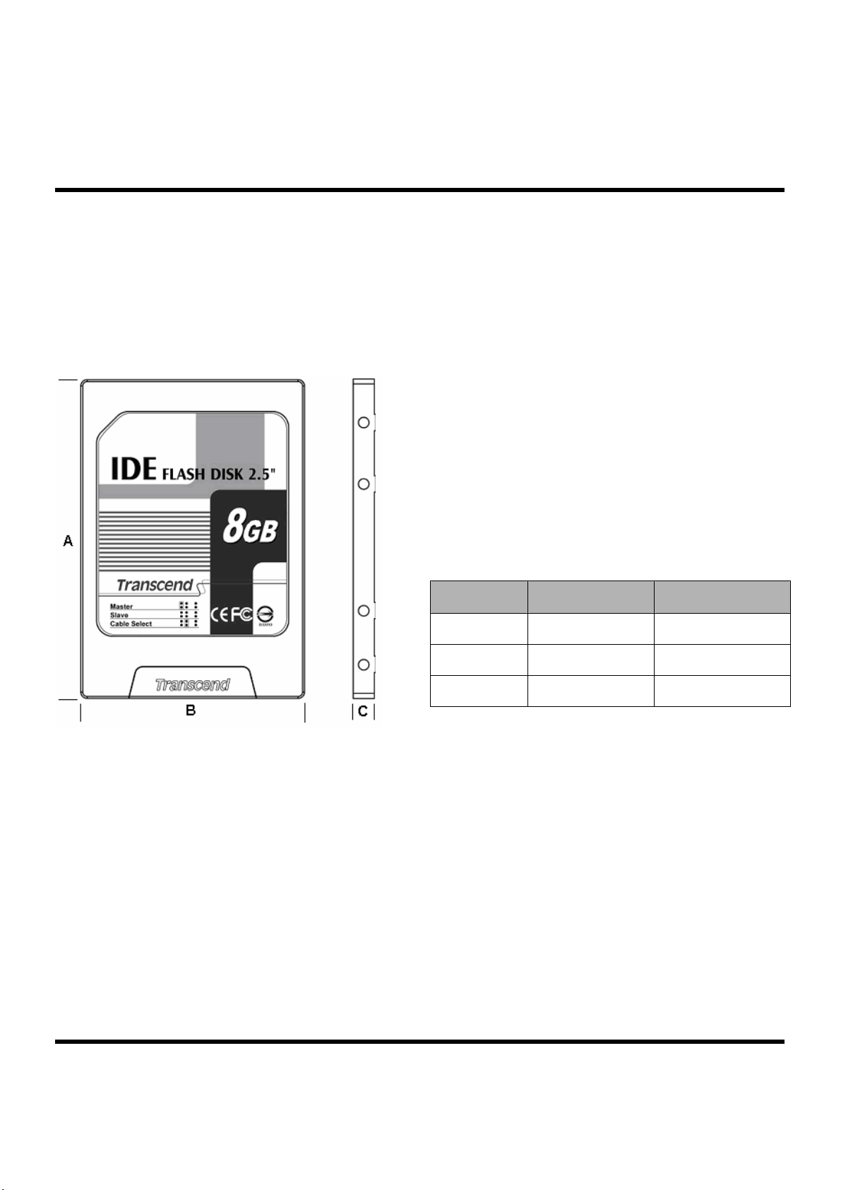
2.5” IDE FLASH DISK
Description
Ideal for use in harsh environments. Transcend’s
2.5” IDE Flash Disks are the best choice for your
specialized industrial computer equipment.
Placement
Features
RoHS compliant
•
• Fully compatible with devices and OS that support the
IDE standard (44-Pin, pitch = 2.00 mm)
• Non-volatile Flash Memory for outstanding data
retention
• Built-in ECC (Error Correction Code) functionality and
wear-leveling algorithm ensures highly reliable of data
transfer
• Supports up to PIO Mode 6 and Ultra DMA Mode 4
• Auto Standby and Sleep Mode supported
• Lower Power Consumption
• Shock resistance
Dimensions
Side Millimeters Inches
A
B
C
100.00 ± 0.40 3.937 ± 0.016
69.85 ± 0.20 2.750 ± 0.008
7.40 ± 0.15 0.292 ± 0.004
Transcend Information Inc.
1
V1.02
Page 2
T
S
2
G
I
F
D
2
T
S
2
G
I
2
G
F
I
F
T
S
Specifications
Physical Specification
Form Factor
Storage Capacities
Dimensions (mm)
Weight
Connector
Power Requirements
Input Voltage
Power Consumption
@25℃)
(
* Note: Base on TS8GIFD25
D
D
2
2
5
5
5
/
T
S
4
G
I
F
D
2
5
/
T
S
8
G
I
F
/
T
S
4
G
I
F
D
2
5
/
T
S
/
T
S
4
G
I
F
D
2
5
/
2.5-inch HDD
2 GB to 8 GB
Length
Width
Height
Mode TYP (mA) MAX (mA)
Write
Read
Standby
Sleep
100.0 0 ± 0.40
69.85 ± 0.20
7.40 ± 0.15
80 g
44-Pin standard IDE/ATA connector (Pitch 2.0 mm)
DC 5V ± 5 %
8
T
S
8
D
G
I
F
D
G
I
F
D
118 133.4
148 158.6
21.8 88.0
17.3 20.6
2
2
2
5
5
5
2.5” IDE FLASH DISK
Environmental Specifications
Operating Temperature
Storage Temperature
Reliability
Data Reliability
Data Retention
Connector Durability
MTBF
Transcend Information Inc.
0
℃ to 70 ℃
- 40
℃ to 85 ℃
Built-in 4 symbol correction ECC (per 512 bytes Sector)
10 years
10,000 times
5,200,000 hours
2
V1.02
Page 3
T
S
2
G
I
F
D
2
5
/
T
S
4
G
I
F
D
2
5
/
T
S
8
G
I
F
T
S
2
G
I
F
D
2
5
/
T
S
4
G
I
F
D
2
5
/
T
S
T
S
2
G
I
F
D
2
5
/
T
S
4
G
I
F
D
2
5
/
Interface Specification
Jumper Settings
Drivers
ATA Compatibility
Performance
Model P/N Capacity Read Write Random Read Random Write Burst R/W Rate
TS2GIFD25 2GB 26.5 MB/s 11.5 MB/s 23.0 MB/s 2.7 MB/s 66.7 MB/s
TS4GIFD25 4GB 26.0 MB/s 11.0 MB/s 22.0 MB/s 2.2 MB/s 66.7 MB/s
TS8GIFD25 8GB 20.4 MB/s 11.0 MB/s 17.6 MB/s 2.9 MB/s 66.7 MB/s
* Note: 25 ℃, GIGABYTE GA-81945GZME-RH, 512MB RAM, IDE interface support UDMA4, Windows
5.00.2195 SP4, benchmark utility HDBENCH (version 3.4003), copied file 100MB
Master/Slave/Cable-select Settings
No Device Driver Required
ATA/ATAPI 5
PIO Modes 0 - 6
UDMA Modes 0 - 4
8
T
S
8
G
G
D
I
F
D
I
F
D
2
2
2
5
5
5
2.5” IDE FLASH DISK
®
2000 Version
Actual Capacity
Model P/N Capacity Cylinder Head Sector
TS2GIFD25 2GB 3954 16 63
TS4GIFD25 4GB 7889 16 63
TS8GIFD25 8GB 15778 16 63
* Note: 2GB FAT format, 4/8GB FAT32 format
Regulations
Compliance
CE, FCC and BSMI
Transcend Information Inc.
3
V1.02
Page 4

T
S
2
G
I
F
D
2
5
/
T
S
4
G
I
F
D
2
5
/
T
S
8
G
I
F
T
S
2
G
I
F
D
2
5
/
T
S
4
G
I
F
D
2
5
/
T
S
T
S
2
G
I
F
D
2
5
/
T
S
4
G
I
F
D
2
5
/
Vibration
Operating
Non-Operating
* Note: Reference to the IEC 60068-2-6 Testing procedures; Operating-Sine wave, 5-800Hz/1 oct., 1.5mm, 3g, 0.5
hr./axis, total 1.5 hrs.
Shock
Operating
Non-Operating
* Note: Reference to the IEC 60068-2-27 Testing procedures; Operating-Half-sine wave, 1500g, 0.5ms, 3 times/dir., total
18 times.
8
T
S
8
G
G
D
I
F
D
I
F
D
2
2
2
5
5
5
3.0G, 5 - 800Hz
3.0G, 5 - 800Hz
1500G, 0.5ms
1500G, 0.5ms
2.5” IDE FLASH DISK
Transcend Information Inc.
4
V1.02
Page 5

T
S
2
G
I
F
D
2
5
/
T
S
4
G
I
F
D
2
5
/
T
S
8
G
I
F
T
S
2
G
I
F
D
2
5
/
T
S
4
G
I
F
D
2
5
/
T
S
T
S
2
G
I
F
D
2
5
/
T
S
4
G
I
F
D
2
5
/
Package Dimensions
Below figure illustrates the Transcend 2.5” IDE Flash Disk. All dimensions are in mm
8
T
S
8
G
G
D
I
F
D
I
F
D
2
2
2
5
5
5
2.5” IDE FLASH DISK
Transcend Information Inc.
5
V1.02
Page 6

T
S
2
G
I
F
D
T
S
2
T
Pin Assignments
G
S
2
G
Pin No. Pin Name Pin No. Pin Name
01 -RESET 02 GND
03 DD7 04 DD8
05 DD6 06 DD9
07 DD5 08 DD10
09 DD4 10 DD11
11 DD3 12 DD12
13 DD2 14 DD13
15 DD1 16 DD14
17 DD0 18 DD15
19 GND 20 KEY-PIN (OPEN)
21 DMARQ 22 GND
23 -DIOW : STOP 24 GND
25 -DIOR : -HDMARDY : HSTROBE 26 GND
27 IORDY : DDMARDY : DSTROBE 28 CSEL
29 -DMACK 30 GND
31 INTRQ 32 IOCS16B
33 DA1 34 -PDIAG : -CBLID
35 DA0 36 DA2
37 -CS0 38 -CS1
39 -DASP 40 GND
41 VCC 42 VCC
43 GND 44 NC (No Connect)
2
I
F
D
I
F
D
2
2
5
5
5
/
T
S
4
G
I
F
D
2
5
/
T
S
8
G
I
F
/
T
S
4
G
I
F
D
2
5
/
T
S
/
T
S
4
G
I
F
D
2
5
/
8
T
S
8
G
G
D
I
F
D
I
F
D
2
2
2
5
5
5
2.5” IDE FLASH DISK
Pin Layout
43
44
Transcend Information Inc.
Cable Select
6
C A
D B
1
2
Master
Slave
C
D
A
B
C A
D B
C A
D B
V1.02
Page 7

T
S
2
G
I
2
2
G
G
F
I
F
I
F
T
S
T
S
Block Diagram
D
D
D
2
2
2
5
5
5
/
T
S
4
G
I
F
D
2
5
/
T
S
8
G
I
F
/
T
S
4
G
I
F
D
2
5
/
T
S
/
T
S
4
G
I
F
D
2
5
/
8
T
S
8
G
G
D
I
F
D
I
F
D
2
2
2
5
5
5
2.5” IDE FLASH DISK
Data bus
44 PIN IDE Connector
Control
Signal
Power
Absolute Maximum Ratings
IDE
Flash Disk
Controller
D00 ~ D07
-CE0, -CE2…
Others
D10 ~ D17
-CE1, -CE3…
Flash Memory
D0 – D7
-CE0
-CE1
-WE…-RE
Flash Memory
D0 – D7
-CE0
-CE1
-WE…-RE
Transcend Information Inc.
7
V1.02
Page 8

T
S
2
G
I
F
D
2
T
S
2
G
I
2
G
F
I
F
T
S
DC Characteristics
D
D
2
2
5
5
5
/
T
S
4
G
I
F
D
2
5
/
T
S
8
G
I
F
/
T
S
4
G
I
F
D
2
5
/
T
S
/
T
S
4
G
I
F
D
2
5
/
8
T
S
8
G
G
D
I
F
D
I
F
D
2
2
2
5
5
5
2.5” IDE FLASH DISK
Transcend Information Inc.
8
V1.02
Page 9

T
S
2
G
I
F
D
2
5
/
T
S
4
G
I
F
D
2
5
/
T
S
8
G
I
F
T
S
2
G
I
F
D
2
5
/
T
S
4
G
I
F
D
2
5
/
T
S
T
S
2
G
I
F
D
2
5
/
T
S
4
G
I
F
D
2
5
/
Command Set
The following table summarizes the command defined in the ATAPI-5 specification and lists the commands supported
by the TS2/4/8GIFD25.
8
T
S
8
G
G
D
I
F
D
I
F
D
2
2
2
5
5
5
2.5” IDE FLASH DISK
Note 1: FR (Feature Register), SC (Sector Count Register), SN (Sector Number Register), CY (Cylinder Low/High
Register), DR (Drive bit of Drive/Head Register), HD (Head No. bit0-bit3 of Drive/Head Register), LBA (Logical Block
Address Mode supported). Y: Set up; -: Not set up; C: The register contains command specific data.
Transcend Information Inc.
9
V1.02
Page 10

T
S
2
G
I
F
D
2
5
/
T
S
2
G
I
F
T
S
2
Ordering Information
G
D
I
F
D
2
2
5
5
/
/
T
S
4
G
I
F
D
2
5
/
T
S
8
G
I
F
T
S
4
G
I
F
D
2
5
/
T
S
T
S
4
G
I
F
D
2
5
/
8
T
S
8
G
G
D
I
F
D
I
F
D
2
2
2
5
5
5
2.5” IDE FLASH DISK
Transcend
Product
Capacity
2GB~8GB
The above technical information is based on industry standard data and has been tested to be reliable. However,
Transcend makes no warranty, either expressed or implied, as to its accuracy and assumes no liability in connection with
the use of this product. Transcend reserves the right to make changes to the specifications at any time without prior notice.
USA
Los Angeles:
E-mail: sales@transcendusa.com
Maryland:
E-mail: sales_md@transcendusa.com
www.transcendusa.com
TAIWAN
No.70, XingZhong Rd., NeiHu Dist., Taipei, Taiwan, R.O.C
TEL +886-2-2792-8000
Fax +886-2-2793-2222
E-mail: sales@transcend.com.tw
www.transcend.com.tw
CHINA
E-mail: sales@transcendchina.com
www.transcendchina.com
GERMANY
E-mail: vertrieb@transcend.de
www.transcend.de
HONG KONG
E-mail: sales@transcend.com.hk
www.transcendchina.com
JAPAN
E-mail: sales@transcend.co.jp
www.transcend.jp
THE NETHERLANDS
E-mail: sales@transcend.nl
www.transcend.nl
United Kingdom
E-mail: sales@transcend-uk.com
www.transcend-uk.com
Form Factor:
25 = 2.5" inch
IDE Flash Disk
Transcend Information Inc.
10
V1.02
 Loading...