

Transcend Information TS64GSSD25S-S, SSD25S, TS64GSSD25S-M, TS128GSSD25S-M, TS32GSSD25S-M User Manual
...Page 1
T
S
8
G
S
S
D
2
5
S
-
S
T
S
8
G
S
S
D
G
G
G
8
2
S
G
G
G
G
G
G
S
S
S
S
S
S
S
S
S
S
S
S
S
S
S
S
S
S
S
S
S
S
S
S
S
D
S
S
D
D
D
D
D
D
S
S
S
S
2
D
D
D
2
2
2
2
D
D
D
D
D
D
T
S
8
G
T
S
1
6
S
S
S
S
S
S
S
S
S
S
S
S
S
S
G
1
6
G
1
6
3
2
G
G
3
2
3
2
6
4
G
6
4
G
6
4
1
2
8
1
2
8
1
2
1
9
2
1
9
2
1
9
T
T
T
T
T
T
T
T
T
T
T
T
T
T
5
S
-
S
5
S
-
S
5
S
-
S
/
M
-
-
S
S
S
S
-
S
/
M
-
S
/
M
S
/
M
-
S
/
M
-
S
/
M
S
/
M
-
S
/
M
-
S
/
M
-
M
-
M
-
M
-
M
-
M
-
M
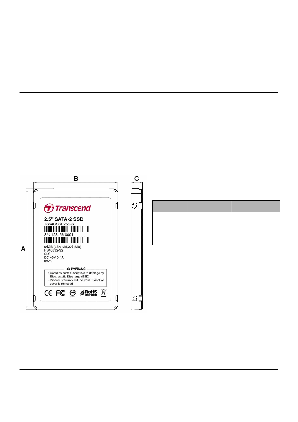
2.5” Solid State Disk
2
5
S
2
5
S
5
S
2
5
S
2
5
S
5
S
2
5
S
2
5
S
2
5
S
2
5
2
5
2
5
S
2
5
2
5
Description
Due to smaller size (fit the standard dimensions of
2.5” SATA Hard Disk Drives), huge capacity, high
speed, and low power consumption, Solid State Disk
is perfect replacement storage device for PCs,
Laptops, gaming systems, and handheld devices.
Placement
Features
• RoHS compliant
• Fully compatible with devices and OS that support the
SATAⅡ 3.0Gbps standard
• Non-volatile Flash Memory for outstanding data
retention
• Built-in ECC (Error Correction Code) functionality and
wear-leveling algorithm ensures highly reliable of data
transfer
• Shock resistance
Dimensions
Side Millimeters Inches
A
B
C
100.00 ± 0.40 3.937 ± 0.016
69.85 ± 0.20 2.750 ± 0.008
9.50 ± 0.15 0.374 ± 0.004
Transcend Information Inc.
1
V1.08
Page 2
T
S
8
G
S
S
D
2
5
S
-
S
T
S
8
G
S
S
D
G
G
G
8
2
S
G
G
G
G
G
G
S
S
S
S
S
S
S
S
S
S
S
S
S
S
S
S
S
S
S
S
S
S
S
S
S
D
S
S
D
D
D
D
D
D
S
S
S
S
2
D
D
D
2
2
2
2
D
D
D
D
D
D
T
S
8
G
T
S
1
6
T
T
T
T
T
T
T
T
T
T
T
T
T
T
Specifications
G
S
1
6
G
S
1
6
S
3
2
G
G
S
3
2
S
3
2
S
6
4
G
S
6
4
G
S
6
4
S
1
2
8
S
1
2
8
S
1
2
S
1
9
2
S
1
9
2
S
1
9
Physical Specification
Form Factor
Storage Capacities
Dimensions (mm)
Input Voltage
Weight
Connector
Environmental Specifications
5
S
-
S
5
S
-
S
5
S
-
S
2
2
5
2
2
5
2
2
2
2
/
5
S
-
S
5
S
-
S
S
-
S
/
5
S
-
S
5
S
-
S
S
-
S
/
5
S
-
S
5
S
-
S
5
S
-
M
2
5
S
-
M
2
5
S
-
M
5
S
-
M
2
5
S
-
M
2
5
S
-
M
/
/
/
/
/
/
M
M
M
M
M
M
M
M
M
Length
Width
Height
2.5” Solid State Disk
2.5-inch HDD
8 GB to 192 GB
100.0 0 ± 0.40
69.85 ± 0.20
9.50 ± 0.15
5V ± 5%
55g ± 5g
SATA 7+15 pins combo connector
0
Operating Temperature
Storage Temperature
Power Requirements
Input Voltage
Mode Max. (mA) Max. (W)
Power Consumption
(8/16/32/64GB)
Power Consumption
(128GB)
Power Consumption
(192GB)
Write
Read
Idle
Write
Read
Idle
Write
Read
Idle
(peak)
(peak)
(peak)
(peak)
(peak)
(peak)
(peak)
(peak)
(peak)
℃ to 70 ℃
℃ to 85 ℃
- 40
5V ± 5%
@25℃
476.1 2.4
426.2 2.1
144.0 0.7
541.6 2.7
461.2 2.3
142.1 0.7
573.3 2.9
483.1 2.4
146.2 0.7
Transcend Information Inc.
2
V1.08
Page 3
T
S
8
T
S
8
T
S
8
T
S
1
T
S
1
T
S
1
T
S
3
T
S
3
T
S
3
T
S
6
T
S
6
T
S
6
T
S
1
T
S
1
T
S
1
T
S
1
T
S
1
T
S
1
Performance
G
G
G
6
6
6
2
2
2
4
4
4
2
2
2
9
9
9
G
G
G
G
G
G
G
G
G
8
8
8
2
2
2
S
S
S
G
G
G
G
G
G
S
S
S
S
S
S
S
S
S
S
S
S
S
S
S
S
S
S
S
S
S
D
D
S
S
S
S
S
S
D
S
S
D
D
D
D
D
D
S
S
S
S
2
2
D
D
D
5
S
-
S
5
S
-
S
2
2
2
2
2
2
2
D
D
D
D
D
D
5
S
-
S
5
S
-
S
/
M
-
-
S
S
S
S
-
S
/
M
-
S
/
M
S
/
M
-
S
/
M
-
S
/
M
S
/
M
-
S
/
M
-
S
/
M
-
M
-
M
-
M
-
M
-
M
-
M
2.5” Solid State Disk
5
S
2
5
S
5
S
5
S
2
5
S
5
S
5
S
2
5
S
2
5
S
2
5
2
5
2
5
S
2
5
2
5
TS8GSSD25S-S 150 MB/s 90 MB/s
TS16GSSD25S-M 150 MB/s 50 MB/s
TS16GSSD25S-S 150 MB/s 100 MB/s
TS32GSSD25S-M 150 MB/s 90 MB/s
TS32GSSD25S-S 150 MB/s 120 MB/s
TS64GSSD25S-M 150 MB/s 90 MB/s
TS64GSSD25S-S 170 MB/s 140 MB/s
TS128GSSD25S-M 150 MB/s 90 MB/s
TS192GSSD25S-M 150 MB/s 90 MB/s
Actual Capacity
TS8GSSD25S-S 15,621,984 15,498 16 63
TS16GSSD25S-M 31,277,056 16,383 16 63
TS16GSSD25S-S 31,277,056 16,383 16 63
TS32GSSD25S-M 62,586,880 16,383 16 63
TS32GSSD25S-S 62,586,880 16,383 16 63
TS64GSSD25S-M 125,206,528 16,383 16 63
TS64GSSD25S-S 125,206,528 16,383 16 63
TS128GSSD25S-M 250,445,824 16,383 16 63
TS192GSSD25S-M 375,685,120 16,383 16 63
Model P/N
Model P/N User Max. LBA Cylinder Head Sector
Sequential Read
Sequential Write
(Max.)
(Max.)
Transcend Information Inc.
3
V1.08
Page 4
T
S
8
G
S
S
D
2
5
S
-
S
T
S
8
G
S
S
D
G
G
G
8
2
S
G
G
G
G
G
G
S
S
S
S
S
S
S
S
S
S
S
S
S
S
S
S
S
S
S
S
S
S
S
S
S
D
S
S
D
D
D
D
D
D
S
S
S
S
2
D
D
D
2
2
2
2
D
D
D
D
D
D
T
S
8
G
T
S
1
6
T
T
T
T
T
T
T
T
T
T
T
T
T
T
* Note: Reference to the IEC 60068-2-6 Testing procedures; Operating-Sine wave, 5-800Hz/1 oct., 1.5mm, 3g, 0.5
hr./axis, total 1.5 hrs.
G
S
1
6
G
S
1
6
S
3
2
G
G
S
3
2
S
3
2
S
6
4
G
S
6
4
G
S
6
4
S
1
2
8
S
1
2
8
S
1
2
S
1
9
2
S
1
9
2
S
1
9
Reliability
Data Reliability
Data Retention
MTBF
Vibration
Operating
Non-Operating
5
S
-
S
5
S
-
S
5
S
-
S
/
M
-
-
S
S
S
S
-
S
/
M
-
S
/
M
S
/
M
-
S
/
M
-
S
/
M
S
/
M
-
S
/
M
-
S
/
M
-
M
-
M
-
M
-
M
-
M
-
M
Supports BCH ECC 8 bits in 512 bytes
10 years
1,000,000 hours
3.0G, 5 - 800Hz
3.0G, 5 - 800Hz
2.5” Solid State Disk
2
5
S
2
5
S
5
S
2
5
S
2
5
S
5
S
2
5
S
2
5
S
2
5
S
2
5
2
5
2
5
S
2
5
2
5
Shock
Operating
Non-Operating
* Note: Reference to the IEC 60068-2-27 Testing procedures; Operating-Half-sine wave, 1500g, 0.5ms, 3 times/dir., total
18 times.
Regulations
Compliance
CE, FCC and BSMI
1500G, 0.5ms
1500G, 0.5ms
Transcend Information Inc.
4
V1.08
Page 5
T
S
8
G
S
S
D
2
5
S
-
S
T
S
8
G
S
S
D
G
G
G
8
2
S
G
G
G
G
G
G
S
S
S
S
S
S
S
S
S
S
S
S
S
S
S
S
S
S
S
S
S
S
S
S
S
D
S
S
D
D
D
D
D
D
S
S
S
S
2
D
D
D
2
2
2
2
D
D
D
D
D
D
T
S
8
G
T
S
1
6
S
S
S
S
S
S
S
S
S
S
S
S
S
S
G
1
6
G
1
6
3
2
G
G
3
2
3
2
6
4
G
6
4
G
6
4
1
2
8
1
2
8
1
2
1
9
2
1
9
2
1
9
T
T
T
T
T
T
T
T
T
T
T
T
T
T
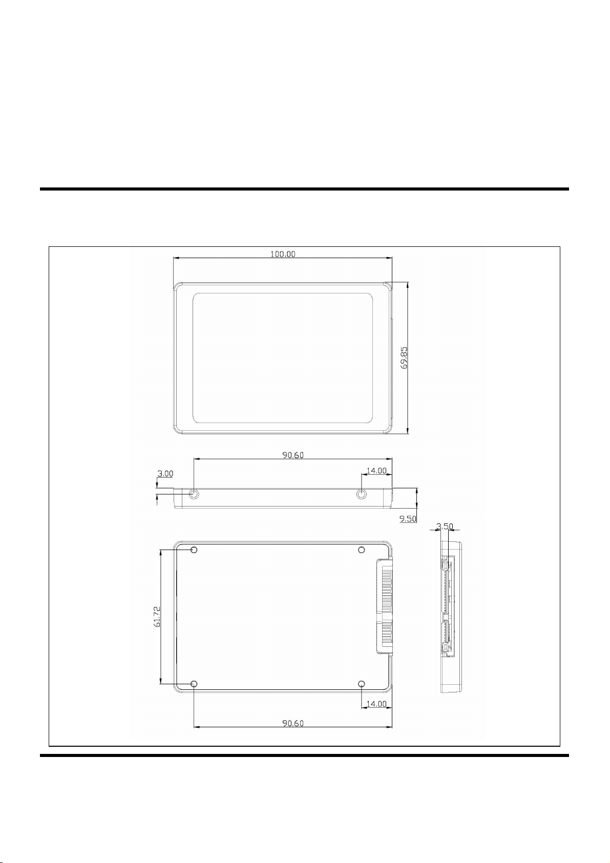
Package Dimensions
Below figure illustrates the Transcend 2.5” SATA Solid State Disk. All dimensions are in mm.
5
S
-
S
5
S
-
S
5
S
-
S
/
M
-
-
S
S
S
S
-
S
/
M
-
S
/
M
S
/
M
-
S
/
M
-
S
/
M
S
/
M
-
S
/
M
-
S
/
M
-
M
-
M
-
M
-
M
-
M
-
M
2
5
S
2
5
S
5
S
2
5
S
2
5
S
5
S
2
5
S
2
5
S
2
5
S
2
5
2
5
2
5
S
2
5
2
5
2.5” Solid State Disk
Transcend Information Inc.
5
V1.08
Page 6
T
S
8
G
S
S
D
2
S
S
S
G
G
G
G
S
S
S
S
S
S
S
S
S
S
S
S
S
S
S
S
S
S
S
S
D
S
S
S
D
S
S
D
D
D
D
D
D
S
S
S
S
2
D
D
D
5
5
2
5
2
2
2
2
2
2
2
2
2
D
D
D
D
D
D
T
S
8
G
T
T
T
T
T
T
T
T
T
T
T
T
T
T
T
T
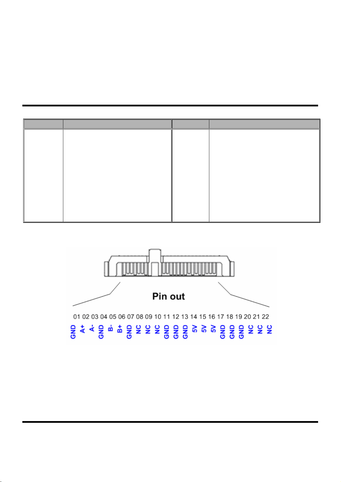
Pin Assignments
S
S
8
G
S
S
1
6
G
S
1
6
G
S
1
6
G
S
3
2
G
G
S
3
2
S
3
2
G
S
6
4
G
S
6
4
G
S
6
4
G
S
1
2
8
S
S
S
G
1
2
8
S
1
2
8
1
9
2
G
1
9
2
S
1
9
2
Pin No. Pin Name Pin No. Pin Name
01 GND 02 A+
03 A- 04 GND
05 B- 06 B+
07 GND 08 NC
09 NC 10 NC
11 GND 12 GND
13 GND 14 5V
15 5V 16 5V
17 GND 18 GND
19 GND 20 NC
21 NC 22 NC
S
S
5
5
5
5
5
5
2
2
2
2
S
5
5
5
2
2
S
S
S
5
5
-
-
S
S
S
S
S
S
5
5
5
5
S
S
-
S
-
S
/
M
-
S
/
M
-
S
/
M
-
S
/
M
-
S
/
M
-
S
/
M
-
S
/
M
-
S
/
M
-
S
/
M
S
-
M
S
-
M
S
-
M
S
S
S
-
M
-
M
-
M
2.5” Solid State Disk
Pin Layout
Transcend Information Inc.
6
V1.08
Page 7
T
S
8
G
S
S
G
6
6
2
2
4
4
2
2
9
9
G
6
2
4
2
9
G
G
G
G
G
G
G
G
G
8
8
8
2
2
2
S
S
G
G
G
G
G
G
S
S
S
S
S
S
S
S
S
S
S
S
S
S
S
S
S
S
S
S
S
S
S
D
D
S
S
S
D
S
S
T
S
8
T
S
8
T
S
1
T
S
1
T
S
1
T
S
3
T
S
3
T
S
3
T
S
6
T
S
6
T
S
6
T
S
1
T
S
1
T
S
1
T
S
1
T
S
1
T
S
1
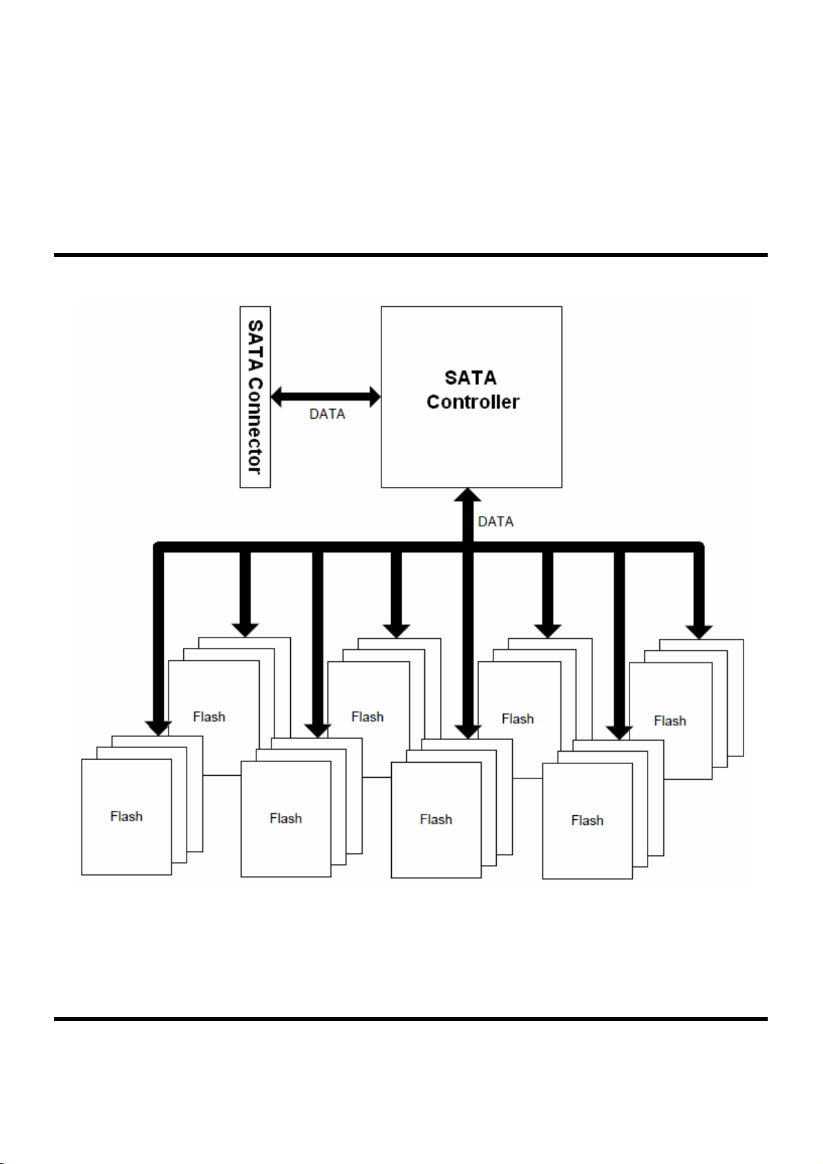
Block Diagram
D
D
D
D
D
D
S
S
S
S
2
2
D
D
D
5
S
-
S
5
S
-
S
2
2
2
2
2
2
2
D
D
D
D
D
D
5
S
-
S
5
S
-
S
/
M
-
-
S
S
S
S
-
S
/
M
-
S
/
M
S
/
M
-
S
/
M
-
S
/
M
S
/
M
-
S
/
M
-
S
/
M
-
M
-
M
-
M
-
M
-
M
-
M
2.5” Solid State Disk
5
S
2
5
S
5
S
5
S
2
5
S
5
S
5
S
2
5
S
2
5
S
2
5
2
5
2
5
S
2
5
2
5
Transcend Information Inc.
7
V1.08
Page 8

T
S
8
G
S
S
D
2
5
S
-
S
T
S
8
G
S
S
D
G
G
G
8
2
S
G
G
G
G
G
G
S
S
S
S
S
S
S
S
S
S
S
S
S
S
S
S
S
S
S
S
S
S
S
S
S
D
S
S
D
D
D
D
D
D
S
S
S
S
2
D
D
D
2
2
2
2
D
D
D
D
D
D
T
S
8
G
T
S
1
6
T
T
T
T
T
T
T
T
T
T
T
T
T
T
Reliability
G
S
1
6
G
S
1
6
S
3
2
G
G
S
3
2
S
3
2
S
6
4
G
S
6
4
G
S
6
4
S
1
2
8
S
1
2
8
S
1
2
S
1
9
2
S
1
9
2
S
1
9
Wear-Leveling algorithm
The controller supports static/dynamic wear leveling. When the host writes data, the controller will find and use the block
with the lowest erase count among the free blocks. This is known as dynamic wear leveling. When the free blocks' erase
count is higher than the data blocks', it will activate the static wear leveling, replacing the not so frequently used user
blocks with the high erase count free blocks.
ECC algorithm
The controller use BCH8 ECC algorithm per 512 bytes. BCH8 can correct up to 8 random error bits within 512 data
bytes.
5
S
-
S
5
S
-
S
5
S
-
S
/
M
-
-
S
S
S
S
-
S
/
M
-
S
/
M
S
/
M
-
S
/
M
-
S
/
M
S
/
M
-
S
/
M
-
S
/
M
-
M
-
M
-
M
-
M
-
M
-
M
2.5” Solid State Disk
2
5
S
2
5
S
5
S
2
5
S
2
5
S
5
S
2
5
S
2
5
S
2
5
S
2
5
2
5
2
5
S
2
5
2
5
Bad-block management
When the flash encounters ECC failed, program fail or erase fail, the controller will mark the block as bad block to
prevent the used of this block and caused data lost later on.
Transcend Information Inc.
8
V1.08
Page 9
T
S
8
G
S
S
D
2
5
S
-
S
T
S
8
G
S
S
D
T
S
8
G
T
S
1
6
T
T
T
T
T
T
T
T
T
T
T
T
T
T
SATA Interface
G
S
1
6
G
S
1
6
S
3
2
G
G
S
3
2
S
3
2
S
6
4
G
S
6
4
G
S
6
4
S
1
2
8
S
1
2
8
S
1
2
S
1
9
2
S
1
9
2
S
1
9
Out of bank signaling
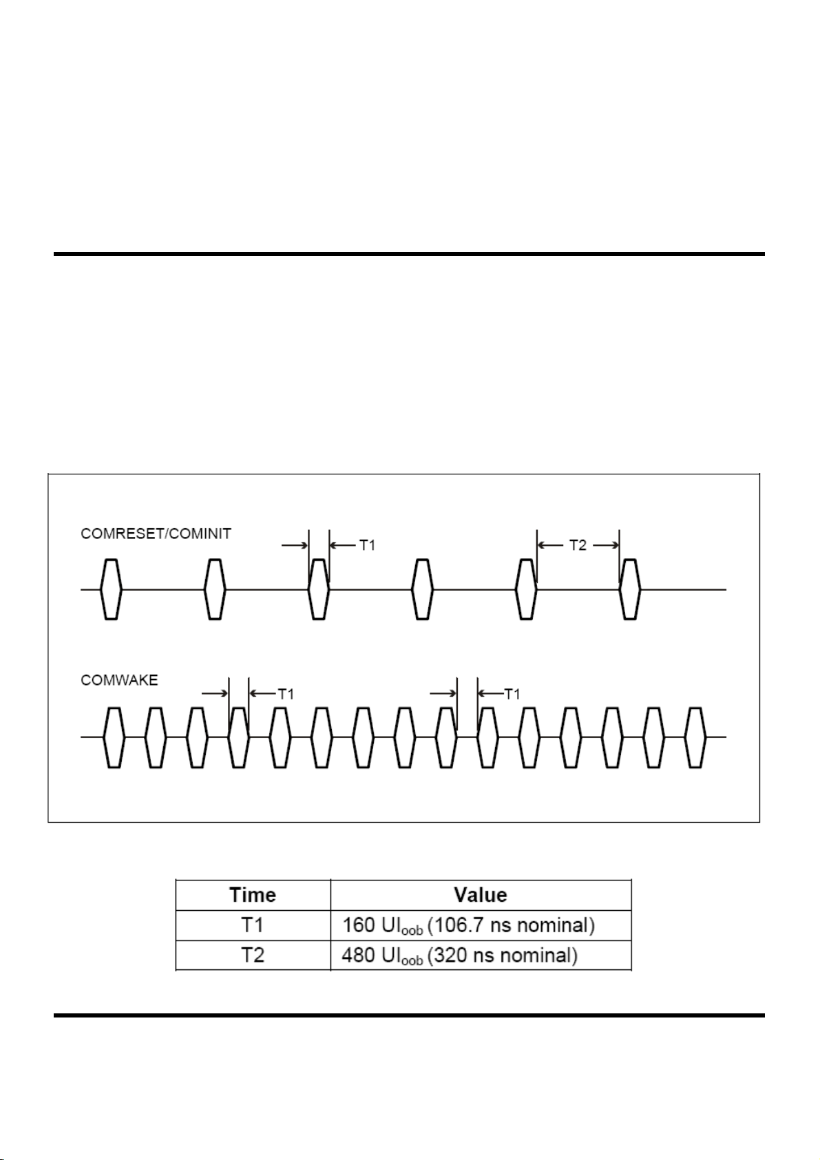
There shall be three Out Of Band (OOB) signals used/detected by the Phy: COMRESET, COMINIT, and COMWAKE.
COMINIT, COMRESET and COMWAKE OOB signaling shall be achieved by transmission of either a burst of four Gen1
ALIGN
2
S
S
D
2
S
S
D
2
S
S
D
G
S
S
D
S
S
D
2
S
S
D
S
S
D
G
S
S
D
2
S
S
D
G
S
S
D
S
S
D
G
S
S
D
G
S
G
G
G
S
S
S
S
S
S
S
D
D
D
D
8
G
2
P primitives or a burst composed of four Gen1 Dwords with each Dword composed of four D24.3 characters, each
5
S
-
S
5
S
-
S
5
S
-
S
/
M
-
-
S
S
S
S
-
S
/
M
-
S
/
M
S
/
M
-
S
/
M
-
S
/
M
S
/
M
-
S
/
M
-
S
/
M
-
M
-
M
-
M
-
M
-
M
-
M
2.5” Solid State Disk
2
5
S
2
5
S
5
S
2
5
S
2
5
S
5
S
2
5
S
2
5
S
2
5
S
2
5
2
5
2
5
S
2
5
2
5
burst having a duration of 160 UI
as depicted in Figure 4 and Table 2.
OOB. Each burst is followed by idle periods (at common-mode levels), having durations
Transcend Information Inc.
Figure 4 : OOB signals
Table 2 : OOB signal times
9
V1.08
Page 10

T
S
8
G
S
S
D
2
5
S
-
S
T
S
8
G
S
S
D
G
G
G
8
2
S
G
G
G
G
G
G
S
S
S
S
S
S
S
S
S
S
S
S
S
S
S
S
S
S
S
S
S
S
S
S
S
D
S
S
D
D
D
D
D
D
S
S
S
S
2
D
D
D
2
2
2
2
D
D
D
D
D
D
T
S
8
G
T
S
1
6
S
S
S
S
S
S
S
S
S
S
S
S
S
S
G
1
6
G
1
6
3
2
G
G
3
2
3
2
6
4
G
6
4
G
6
4
1
2
8
1
2
8
1
2
1
9
2
1
9
2
1
9
T
T
T
T
T
T
T
T
T
T
T
T
T
T
COMRESET
COMRESET always originates from the host controller, and forces a hardware reset in the device. It is indicated by
transmitting bursts of data separated by an idle bus condition. The OOB COMRESET signal shall consist of no less than
six data bursts, including inter-burst temporal spacing. The COMRESET signal shall be:
1) Sustained/continued uninterrupted as long as the system hard reset is asserted, or
2) Started during the system hardware reset and ended some time after the negation of system hardware reset, or
3) Transmitted immediately following the negation of the system hardware reset signal.
The host controller shall ignore any signal received from the device from the assertion of the hardware reset signal until
the COMRESET signal is transmitted. Each burst shall be 160 Gen1 UI’s long (106.7 ns) and each inter-burst idle state
5
S
-
S
5
S
-
S
5
S
-
S
/
M
-
-
S
S
S
S
-
S
/
M
-
S
/
M
S
/
M
-
S
/
M
-
S
/
M
S
/
M
-
S
/
M
-
S
/
M
-
M
-
M
-
M
-
M
-
M
-
M
2.5” Solid State Disk
2
5
S
2
5
S
5
S
2
5
S
2
5
S
5
S
2
5
S
2
5
S
2
5
S
2
5
2
5
2
5
S
2
5
2
5
shall be 480 Gen1 UI’s long (320 ns). A COMRESET detector looksfor four consecutive bursts with 320 ns spacing
(nominal). Any spacing less than 175 ns or greater than 525 ns shall invalidate the COMRESET detector output. The
COMRESET interface signal to the Phy layer shall initiate the Reset sequence shown in Figure 5 below. The interface
shall be held inactive for at least 525 ns after the last burst to ensure far-end detector detects the negation properly.
Transcend Information Inc.
10
V1.08
Page 11
T
S
8
G
S
S
D
2
5
S
-
S
T
S
8
G
S
S
D
G
G
G
8
2
S
G
G
G
G
G
G
S
S
S
S
S
S
S
S
S
S
S
S
S
S
S
S
S
S
S
S
S
S
S
S
S
D
S
S
D
D
D
D
D
D
S
S
S
S
2
D
D
D
2
2
2
2
D
D
D
D
D
D
T
S
8
G
T
S
1
6
S
S
S
S
S
S
S
S
S
S
S
S
S
S
G
1
6
G
1
6
3
2
G
G
3
2
3
2
6
4
G
6
4
G
6
4
1
2
8
1
2
8
1
2
1
9
2
1
9
2
1
9
T
T
T
T
T
T
T
T
T
T
T
T
T
T
5
S
-
S
5
S
-
S
5
S
-
S
/
M
-
-
S
S
S
S
-
S
/
M
-
S
/
M
S
/
M
-
S
/
M
-
S
/
M
S
/
M
-
S
/
M
-
S
/
M
-
M
-
M
-
M
-
M
-
M
-
M
2.5” Solid State Disk
2
5
S
2
5
S
5
S
2
5
S
2
5
S
5
S
2
5
S
2
5
S
2
5
S
2
5
2
5
2
5
S
2
5
2
5
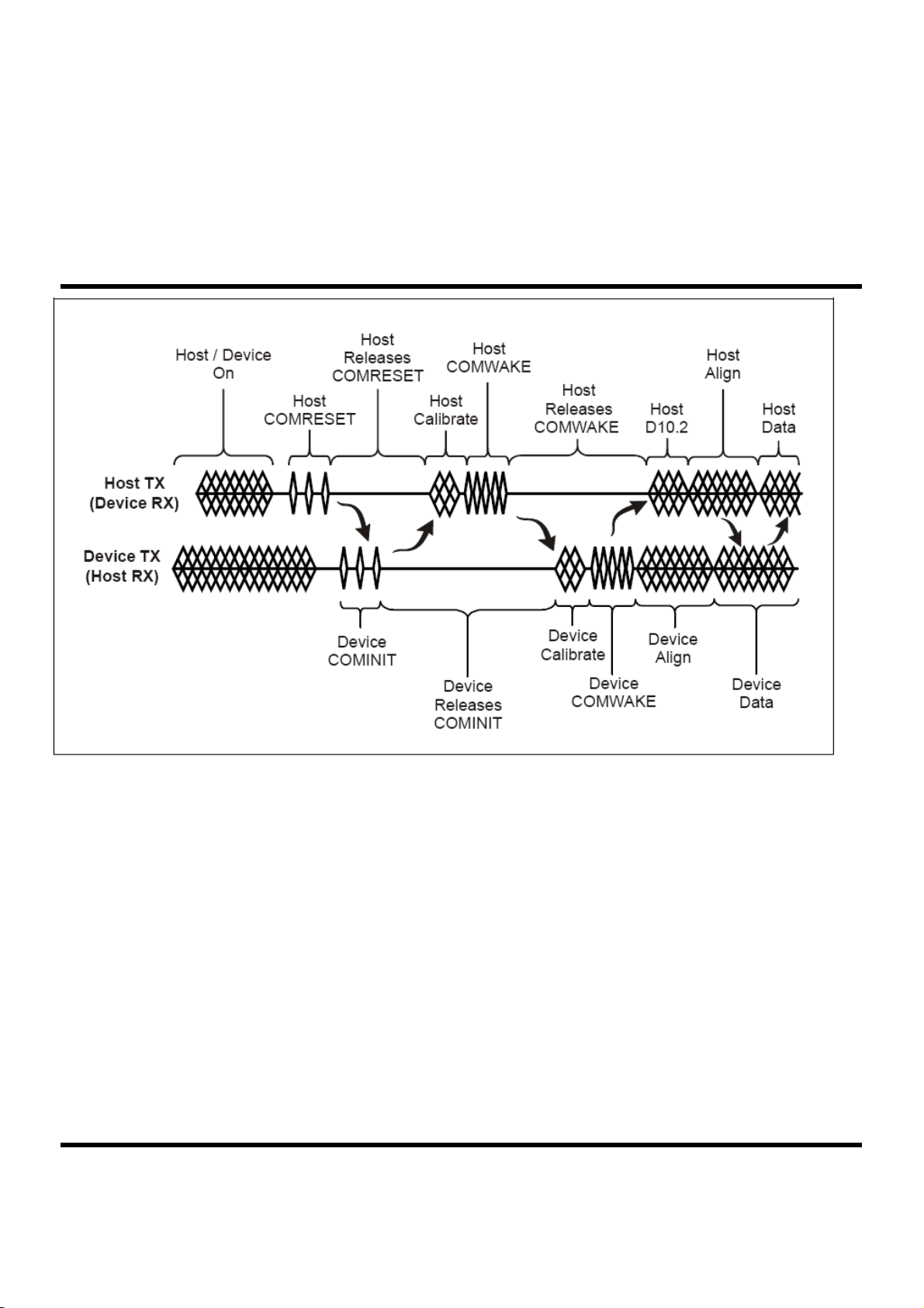
Description:
1. Host/device are powered and operating normally with some form of active communication.
2. Some condition in the host causes the host to issue COMRESET
3. Host releases COMRESET. Once the condition causing the COMRESET is released, the host releases the
COMRESET signal and puts the bus in a quiescent condition.
4. Device issues COMINIT – When the device detects the release of COMRESET, it responds with a COMINIT. This is
also the entry point if the device is late starting. The device may initiate communications at any time by issuing a COMINIT.
5. Host calibrates and issues a COMWAKE.
6. Device responds – The device detects the COMWAKE sequence on its RX pair and calibrates its transmitter (optional).
Following calibration the device sends a six burst COMWAKE sequence and then sends a continuous stream of the
ALIGN sequence starting at the device's highest supported speed. After ALIGNP Dwords have been sent
Transcend Information Inc.
Figure 5 : comreset sequence
11
V1.08
Page 12

T
S
8
G
S
S
D
2
5
S
-
S
T
S
8
G
S
S
D
G
G
G
8
2
S
G
G
G
G
G
G
S
S
S
S
S
S
S
S
S
S
S
S
S
S
S
S
S
S
S
S
S
S
S
S
S
D
S
S
D
D
D
D
D
D
S
S
S
S
2
D
D
D
2
2
2
2
D
D
D
D
D
D
T
S
8
G
T
S
1
6
S
S
S
S
S
S
S
S
S
S
S
S
S
S
G
1
6
G
1
6
3
2
G
G
3
2
3
2
6
4
G
6
4
G
6
4
1
2
8
1
2
8
1
2
1
9
2
1
9
2
1
9
T
T
T
T
T
T
T
T
T
T
T
T
T
T
for 54.6us (2048 nominal Gen1 Dword times) without a response from the host as determined by detection of ALIGNP
primitives received from the host, the device assumes that the host cannot communicate at that speed. If additional
speeds are available the device tries the next lower supported speed by sending ALIGNP Dwords at that rate for
54.6 us (2048 nominal Gen1 Dword times.) This step is repeated for as many slower speeds as are supported. Once the
lowest speed has been reached without response from the host, the device enters an error state.
7. Host locks – after detecting the COMWAKE, the host starts transmitting D10.2 characters at its lowest supported rate.
Meanwhile, the host receiver locks to the ALIGN sequence and, when ready, returns the ALIGN sequence to the device at
the same speed as received. A host shall be designed such that it acquires lock in 54.6us (2048
nominal Gen1 Dword times) at any given speed. The host should allow for at least 873.8 us (32768 nominal Gen1 Dword
times) after detecting the release of COMWAKE to receive the first ALIGNP. This ensures interoperability with
5
S
-
S
5
S
-
S
5
S
-
S
/
M
-
-
S
S
S
S
-
S
/
M
-
S
/
M
S
/
M
-
S
/
M
-
S
/
M
S
/
M
-
S
/
M
-
S
/
M
-
M
-
M
-
M
-
M
-
M
-
M
2.5” Solid State Disk
2
5
S
2
5
S
5
S
2
5
S
2
5
S
5
S
2
5
S
2
5
S
2
5
S
2
5
2
5
2
5
S
2
5
2
5
multi-generational and synchronous designs. If no ALIGNP is received within 873.8 us (32768 nominal Gen1 Dword
times) the host restarts the power-on sequence – repeating indefinitely until told to stop by the Application layer.
8. Device locks – the device locks to the ALIGN sequence and, when ready, sends SYNCP indicating it is ready to start
normal operation.
9. Upon receipt of three back-to-back non-ALIGNP primitives, the communication link is established and normal operation
may begin.
COMINIT
COMINIT always originates from the drive and requests a communication initialization. It is electrically identical to the
COMRESET signal except that it originates from the device and is sent to the host. It is used by the device to request a
reset from the host in accordance to the sequence shown in Figure 6, below.
Transcend Information Inc.
12
V1.08
Page 13

T
S
8
G
S
S
D
2
5
S
-
S
T
S
8
G
S
S
D
G
G
G
8
2
S
G
G
G
G
G
G
S
S
S
S
S
S
S
S
S
S
S
S
S
S
S
S
S
S
S
S
S
S
S
S
S
D
S
S
D
D
D
D
D
D
S
S
S
S
2
D
D
D
2
2
2
2
D
D
D
D
D
D
T
S
8
G
T
S
1
6
S
S
S
S
S
S
S
S
S
S
S
S
S
S
G
1
6
G
1
6
3
2
G
G
3
2
3
2
6
4
G
6
4
G
6
4
1
2
8
1
2
8
1
2
1
9
2
1
9
2
1
9
T
T
T
T
T
T
T
T
T
T
T
T
T
T
5
S
-
S
5
S
-
S
5
S
-
S
/
M
-
-
S
S
S
S
-
S
/
M
-
S
/
M
S
/
M
-
S
/
M
-
S
/
M
S
/
M
-
S
/
M
-
S
/
M
-
M
-
M
-
M
-
M
-
M
-
M
2.5” Solid State Disk
2
5
S
2
5
S
5
S
2
5
S
2
5
S
5
S
2
5
S
2
5
S
2
5
S
2
5
2
5
2
5
S
2
5
2
5
Figure 6 : cominit sequence
Description:
1. Host/device are powered and operating normally with some form of active communication.
2. Some condition in the device causes the device to issues a COMINIT
3. Host calibrates and issues a COMWAKE.
4. Device responds – The device detects the COMWAKE sequence on its RX pair and calibrates its transmitter (optional).
Following calibration the device sends a six burst COMWAKE sequence and then sends a continuous stream of the
ALIGN sequence starting at the device's highest supported speed. After ALIGN
nominal Gen1 Dword times) without a response from the host as determined by detection of ALIGN
from the host, the device assumes that the host cannot communicate at that speed. If additional speeds are available the
device tries the next lower supported speed by sending ALIGN
Dword times.) This step is repeated for as many slower speeds as are supported. Once the lowest speed has been
reached without response from the host, the device enters an error state.
Transcend Information Inc.
13
P Dwords at that rate for 54.6 us (2048 nominal Gen1
P Dwords have been sent for 54.6 us (2048
P primitives received
V1.08
Page 14

T
S
8
G
S
S
D
2
5
S
-
S
T
S
8
G
S
S
D
G
G
G
8
2
S
G
G
G
G
G
G
S
S
S
S
S
S
S
S
S
S
S
S
S
S
S
S
S
S
S
S
S
S
S
S
S
D
S
S
D
D
D
D
D
D
S
S
S
S
2
D
D
D
2
2
2
2
D
D
D
D
D
D
T
S
8
G
T
S
1
6
S
S
S
S
S
S
S
S
S
S
S
S
S
S
G
1
6
G
1
6
3
2
G
G
3
2
3
2
6
4
G
6
4
G
6
4
1
2
8
1
2
8
1
2
1
9
2
1
9
2
1
9
T
T
T
T
T
T
T
T
T
T
T
T
T
T
5. Host locks – after detecting the COMWAKE, the host starts transmitting D10.2 characters at its lowest supported rate.
Meanwhile, the host receiver locks to the ALIGN sequence and, when ready, returns the ALIGN sequence to the device at
the same speed as received. A host shall be designed such that it acquires lock in 54.6 us (2048 nominal Gen1 Dword
times) at any given speed. The host should allow for at least 873.8 us (32768 nominal Gen1 Dword times) after detecting
5
S
-
S
5
S
-
S
5
S
-
S
/
M
-
-
S
S
S
S
-
S
/
M
-
S
/
M
S
/
M
-
S
/
M
-
S
/
M
S
/
M
-
S
/
M
-
S
/
M
-
M
-
M
-
M
-
M
-
M
-
M
2.5” Solid State Disk
2
5
S
2
5
S
5
S
2
5
S
2
5
S
5
S
2
5
S
2
5
S
2
5
S
2
5
2
5
2
5
S
2
5
2
5
the release of COMWAKE to receive the first ALIGN
synchronous designs. If no ALIGN
power-on sequence – repeating indefinitely until told to stop by the Application layer. 6. Device locks – the device locks to
the ALIGN sequence and, when ready, sends SYNC
6. Upon receipt of three back-to-back non-ALIGN
may begin.
Power on sequence timing diagram
The following timing diagrams and descriptions are provided for clarity and are informative.
P is received within 873.8 us (32768 nominal Gen1 Dword times) the host restarts the
P primitives, the communication link is established and normal operation
P. This ensures interoperability with multi-generational and
P indicating it is ready to start normal operation.
Transcend Information Inc.
Figure 7 : power on sequence
14
V1.08
Page 15

T
S
8
G
S
S
D
2
5
S
-
S
T
S
8
G
S
S
D
G
G
G
8
2
S
G
G
G
G
G
G
S
S
S
S
S
S
S
S
S
S
S
S
S
S
S
S
S
S
S
S
S
S
S
S
S
D
S
S
D
D
D
D
D
D
S
S
S
S
2
D
D
D
2
2
2
2
D
D
D
D
D
D
T
S
8
G
T
S
1
6
S
S
S
S
S
S
S
S
S
S
S
S
S
S
G
1
6
G
1
6
3
2
G
G
3
2
3
2
6
4
G
6
4
G
6
4
1
2
8
1
2
8
1
2
1
9
2
1
9
2
1
9
T
T
T
T
T
T
T
T
T
T
T
T
T
T
Description:
1. Host/device power-off - Host and device power-off.
2. Power is applied - Host side signal conditioning pulls TX and RX pairs to neutral state (common mode voltage).
3. Host issues COMRESET
4. Host releases COMRESET. Once the power-on reset is released, the host releases the COMRESET signal and puts
the bus in a quiescent condition.
5. Device issues COMINIT – When the device detects the release of COMRESET, it responds with a COMINIT. This is
also the entry point if the device is late starting. The device may initiate communications at any time by issuing a COMINIT.
6. Host calibrates and issues a COMWAKE.
7. Device responds – The device detects the COMWAKE sequence on its RX pair and calibrates its transmitter (optional).
5
S
-
S
5
S
-
S
5
S
-
S
/
M
-
-
S
S
S
S
-
S
/
M
-
S
/
M
S
/
M
-
S
/
M
-
S
/
M
S
/
M
-
S
/
M
-
S
/
M
-
M
-
M
-
M
-
M
-
M
-
M
2.5” Solid State Disk
2
5
S
2
5
S
5
S
2
5
S
2
5
S
5
S
2
5
S
2
5
S
2
5
S
2
5
2
5
2
5
S
2
5
2
5
Following calibration the device sends a six burst COMWAKE sequence and then sends a continuous stream of the
ALIGN sequence starting at the device's highest supported speed. After ALIGN
(2048 nominal Gen1 Dword times) without a response from the host as determined by detection of ALIGN
received from the host, the device assumes that the host cannot communicate at that speed. If additional speeds are
available the device tries the next lower supported speed by sending ALIGN
nominal Gen1 Dword times.) This step is repeated for as many slower speeds as are supported. Once the lowest speed
has been reached without response from the host, the device shall enter an error state.
8. Host locks – after detecting the COMWAKE, the host starts transmitting D10.2 characters at its lowest supported rate.
Meanwhile, the host receiver locks to the ALIGN sequence and, when ready, returns the ALIGN sequence to the device at
the same speed as received. A host shall be designed such that it acquires lock in 54.6 us (2048 nominal Gen1 Dword
times) at any given speed. The host should allow for at least 873.8 us (32768 nominal Gen1 Dword times) after detecting
the release of COMWAKE to receive the first ALIGN
synchronous designs. If no ALIGN
power-on sequence – repeating indefinitely until told to stop by the Application layer.
9. Device locks – the device locks to the ALIGN sequence and, when ready, sends the SYNC
ready to start normal operation.
10. Upon receipt of three back-to-back non-ALIGN
P is received within 873.8 us (32768 nominal Gen1 Dword times) the host restarts the
P primitives, the communication link is established and normal operation
P. This insures interoperability with multi-generational and
P primitives have been sent for 54.6 us
P primitives
P primitives at that rate for 54.6 us (2048
P primitive indicating it is
may begin.
ATA command register
This table with the following paragraphs summarizes the ATA command set.
Transcend Information Inc.
15
V1.08
Page 16

T
S
8
G
S
S
D
2
5
S
-
S
T
S
8
G
S
S
D
G
G
G
8
2
S
G
G
G
G
G
G
S
S
S
S
S
S
S
S
S
S
S
S
S
S
S
S
S
S
S
S
S
S
S
S
S
D
S
S
D
D
D
D
D
D
S
S
S
S
2
D
D
D
2
2
2
2
D
D
D
D
D
D
T
S
8
G
T
S
1
6
S
S
S
S
S
S
S
S
S
S
S
S
S
S
G
1
6
G
1
6
3
2
G
G
3
2
3
2
6
4
G
6
4
G
6
4
1
2
8
1
2
8
1
2
1
9
2
1
9
2
1
9
T
T
T
T
T
T
T
T
T
T
T
T
T
T
5
S
-
S
5
S
-
S
5
S
-
S
/
M
-
-
S
S
S
S
-
S
/
M
-
S
/
M
S
/
M
-
S
/
M
-
S
/
M
S
/
M
-
S
/
M
-
S
/
M
-
M
-
M
-
M
-
M
-
M
-
M
Command Table
2.5” Solid State Disk
2
5
S
2
5
S
5
S
2
5
S
2
5
S
5
S
2
5
S
2
5
S
2
5
S
2
5
2
5
2
5
S
2
5
2
5
Command Name Code
SC SN CY DR HD FT
CHECK POWER MODE E5h X X X O X X
EXECUTE DIAGNOSTICS 90h X X X O X X
FLUSH CACHE E7h X X X O O X
FLUSH CACHE EXT EAh X X X O O X
IDENTIFY DEVICE ECh X X X O X X
IDLE E3h O X X O X X
IDLE IMMEDIATE E1h X X X O X X
INITIALIZE DEVICE PARAMETERS 91h O X X O O X
READ BUFFER E4h X X X O X X
READ DMA C8h or C9h O O O O O X
READ DMA EXT 25h O O O O O X
READ FPDMA QUEUED 60h O O O O O O
READ LOG EXT 2Fh O O O O O O
READ MULTIPLE C4h O O O O O X
READ MULTIPLE EXT 29h O O O O O X
PARAMETERS USED
READ SECTOR(S) 20h or 21h O O O O O X
READ SECTOR(S) EXT 24h O O O O O X
READ VERIFY SECTOR(S) 40h or 41h O O O O O X
READ VERIFY SECTOR(S) EXT 42h O O O O O X
RECALIBRATE 10h X X X O X X
SECURITY DISABLE PASSWORD F6h X X X O X X
SECURITY ERASE PREPARE F3h X X X O X X
SECURITY ERASE UNIT F4h X X X O X X
SECURITY FREEZE LOCK F5h X X X O X X
SECURITY SET PASSWORD F1h X X X O X X
SECURITY UNLOCK F2h X X X O X X
SEEK 7xh X X O O O X
Transcend Information Inc.
16
V1.08
Page 17

T
S
8
G
S
S
D
2
5
S
-
S
T
S
8
G
S
S
D
T
S
8
G
T
S
1
6
S
S
S
S
S
S
S
S
S
S
S
S
S
S
G
1
6
G
1
6
3
2
G
G
3
2
3
2
6
4
G
6
4
G
6
4
1
2
8
1
2
8
1
2
1
9
2
1
9
2
1
9
T
T
T
T
T
T
T
T
T
T
T
T
T
T
2
S
S
D
2
S
S
D
2
S
S
D
G
S
S
D
S
S
D
2
S
S
D
S
S
D
G
S
S
D
2
S
S
D
G
S
S
D
S
S
D
G
S
S
D
G
S
8
G
2
D
G
S
S
S
D
G
S
S
D
G
S
S
D
SET FEATURES EFh O X X O X O
SET MULTIPLE MODE C6h O X X O X X
SLEEP E6h X X X O X X
SMART B0h X X O O X O
STANDBY E2h X X X O X X
STANDBY IMMEDIATE E0h X X X O X X
WRITE BUFFER E8h X X X O X X
WRITE DMA CAh or CBh O O O O O X
WRITE DMA EXT 35h O O O O O X
WRITE DMA FUA EXT 3Dh O O O O O X
5
S
-
S
5
S
-
S
5
S
-
S
/
M
-
-
S
S
S
S
-
S
/
M
-
S
/
M
S
/
M
-
S
/
M
-
S
/
M
S
/
M
-
S
/
M
-
S
/
M
-
M
-
M
-
M
-
M
-
M
-
M
2.5” Solid State Disk
2
5
S
2
5
S
5
S
2
5
S
2
5
S
5
S
2
5
S
2
5
S
2
5
S
2
5
2
5
2
5
S
2
5
2
5
WRITE FPDMA QUEUED 61h O O O O O O
WRITE MULTIPLE C5h O O O O O X
WRITE MULTIPLE EXT 39h O O O O O X
WRITE MULTIPLE FUA EXT CEh O O O O O X
WRITE SECTOR(S) 30h or 31h O O O O O X
WRITE SECTOR(S) EXT 34h O O O O O X
Note:
O = Valid, X = Don't care
SC = Sector Count Register
SN = Sector Number Register
CY = Cylinder Low/High Register
DR = DEVICE SELECT Bit (DEVICE/HEAD Register Bit 4)
HD = HEAD SELECT Bit (DEVICE/HEAD Register Bit 3-0)
FT = Features Register
Transcend Information Inc.
17
V1.08
Page 18

T
S
8
G
S
S
D
2
5
S
-
S
T
S
8
G
S
S
D
G
G
G
8
2
S
G
G
G
G
G
G
S
S
S
S
S
S
S
S
S
S
S
S
S
S
S
S
S
S
S
S
S
S
S
S
S
D
S
S
D
D
D
D
D
D
S
S
S
S
2
D
D
D
2
2
2
2
D
D
D
D
D
D
T
S
8
G
T
S
1
6
S
S
S
S
S
S
S
S
S
S
S
S
S
S
G
1
6
G
1
6
3
2
G
G
3
2
3
2
6
4
G
6
4
G
6
4
1
2
8
1
2
8
1
2
1
9
2
1
9
2
1
9
T
T
T
T
T
T
T
T
T
T
T
T
T
T
ATA Command Specifications
CHECK POWER MODE (E5h)
The host can use this command to determine the current power management mode.
EXECUTE DIAGNOSTICS (90h)
This command performs the internal diagnostic tests implemented by the drive.
FLUSH CACHE (E7h)
This command is used by the host to request the device to flush the write cache. If there is data in the write cache, that
data shall be written to the media. The BSY bit shall remain set to one until all data has been successfully written or an
5
S
-
S
5
S
-
S
5
S
-
S
/
M
-
-
S
S
S
S
-
S
/
M
-
S
/
M
S
/
M
-
S
/
M
-
S
/
M
S
/
M
-
S
/
M
-
S
/
M
-
M
-
M
-
M
-
M
-
M
-
M
2.5” Solid State Disk
2
5
S
2
5
S
5
S
2
5
S
2
5
S
5
S
2
5
S
2
5
S
2
5
S
2
5
2
5
2
5
S
2
5
2
5
error occurs.
FLUSH CACHE EXT (EAh)
48-bit feature set mandatory command. This command is used by the host to request the device to flush the write cache.
If there is data in the write cache, that data shall be written to the media. The BSY bit shall remain set to one until all data
has been successfully written or an error occurs.
IDENTIFY DEVICE (ECh)
This commands read out 512Bytes of drive parameter information. Parameter Information consists of the arrangement
and value as shown in the following table. This command enables the host to receive the Identify Drive Information from
the device.
Transcend Information Inc.
18
V1.08
Page 19

T
S
8
G
S
S
D
2
5
S
-
S
T
S
8
G
S
S
D
G
G
G
8
2
S
G
G
G
G
G
G
S
S
S
S
S
S
S
S
S
S
S
S
S
S
S
S
S
S
S
S
S
S
S
S
S
D
S
S
D
D
D
D
D
D
S
S
S
S
2
D
D
D
2
2
2
2
D
D
D
D
D
D
T
S
8
G
T
S
1
6
T
T
T
T
T
T
T
T
T
T
T
T
T
T
G
S
1
6
G
S
1
6
S
3
2
G
G
S
3
2
S
3
2
S
6
4
G
S
6
4
G
S
6
4
S
1
2
8
S
1
2
8
S
1
2
S
1
9
2
S
1
9
2
S
1
9
Word Value F/V Description
0 0040h
1 3FFFh
2 C837h
3 0010h
4-5 0000h
6 003Fh
7-8 0000h
9 0000h
10-19 XXXXh
20-21 0000h
22 0000h
23-26 XXXXh
27-46 XXXXh
47 8001h
48 0000h
49 2F00h
50 4000h
5
S
-
S
5
S
-
S
5
S
-
S
/
M
2
5
S
2
5
S
5
S
2
5
S
2
5
S
5
S
2
5
S
2
5
S
2
5
S
2
5
2
5
2
5
S
2
5
2
5
-
S
/
M
-
S
/
M
-
S
/
M
-
S
/
M
-
S
/
M
-
S
/
M
-
S
/
M
-
S
/
M
-
M
S
-
M
S
-
M
-
M
S
-
M
S
-
M
Identify Device Information Default Value
General configuration bit-significant information:
F
15 0 = ATA device
X
14-8 Retired
X
7-6 Obsolete
X
5-3 Retired
V
2 Reserved
X
1 Retired
0 Reserved
F Number of logical cylinders
V Specific configuration
F Number of logical heads
X Retired
F Number of logical sector per logical track
Reserved for assignment by the CompactFlash_ Association
X Retired
F Serial number (20 ASCII characters)
X Retired
X Obsolete
F Firmware revision (8 ASCII characters)
F Model number (40 ASCII characters)
F
15-8 80h
F
7-0 00h = Reserved
F
F Reserved
Capabilities
15-14 Reserved for the IDENTIFY PACKET DEVICE command.
F
13 1 = Standby timer values as specified in this standard are supported
12 Reserved for the IDENTIFY PACKET DEVICE command.
F
11 1 = IORDY supported
F
10 1 = IORDY may be disabled
F
9 1 = LBA supported
F
8 1 = DMA supported.
X
7-0 Retired
Capabilities
01h = Maximum number of 1 sectors on READ/WRITE MULTIPLE commands
0 = Standby timer values shall be managed by the device
0 = IORDY may be supported
2.5” Solid State Disk
Transcend Information Inc.
19
V1.08
Page 20

T
S
8
G
S
S
D
G
G
G
G
G
G
8
8
2
2
S
S
G
G
G
G
G
G
S
S
S
S
S
S
S
S
S
S
S
S
S
S
S
S
S
S
S
S
S
S
S
D
S
S
S
D
S
S
D
D
D
D
D
D
S
S
S
S
2
2
D
D
D
T
S
8
G
T
S
8
G
T
S
1
6
T
T
T
T
T
T
T
T
T
T
T
T
T
T
G
S
1
6
S
1
6
S
3
2
G
S
3
2
S
3
2
S
6
4
G
S
6
4
S
6
4
S
1
2
8
S
1
2
S
1
2
S
1
9
2
S
1
9
S
1
9
51 0000h
52 0000h
53 0007h
54 XXXXh
55 00XXh
56 XXXXh
57-58 XXXXh
59 0101h
60-61 XXXXh
62 0000h
63 0007h
64 0003h
65 0078h
66 0078h
67 0078h
5
S
-
S
5
S
-
S
2
2
2
2
2
2
2
D
D
D
D
D
D
5
S
-
S
5
S
-
S
/
M
5
S
2
5
S
5
S
5
S
2
5
S
5
S
5
S
2
5
S
2
5
S
2
5
2
5
2
5
S
2
5
2
5
-
S
/
M
-
S
/
M
-
S
/
M
-
S
/
M
-
S
/
M
-
S
/
M
-
S
/
M
-
S
/
M
-
M
S
-
M
S
-
M
-
M
S
-
M
S
-
M
F
15 Shall be cleared to zero.
F
14 Shall be set to one.
13-2 Reserved.
X
1 Obsolete
F
0 Shall be set to one to indicate a device specific Standby timer value minimum.
F 15-8 PIO data transfer cycle timing mode
7-0 Reserved
X Obsolete
F
15-3 Reserved
F
2 1 = the fields reported in word 88 are valid
F
1 1 = the fields reported in words 70:64 are valid
X
0 1 = the fields reported in words 58:54 are valid
X Number of current cylinders
X Number of current heads
X Number of current sector per track
X Current capacity in sectors
15-9 Reserved
V
8 1 = Multiple sector setting is valid
V
7-0 xxh = Setting for number of sectors that shall be transferred per interrupt on R/W Multiple command
F Total number of user addressable sectors
X Obsolete
F
15-11 Reserved
V
10 1 = Multiword DMA mode 2 is selected
V
9 1 = Multiword DMA mode 1 is selected
V
8 1 = Multiword DMA mode 0 is selected
7-3 Reserved
F
2 1 = Multiword DMA mode 2 and below are supported
F
1 1 = Multiword DMA mode 1 and below are supported
F
0 1 = Multiword DMA mode 0 is supported
15-8 Reserved
F
7-0 Advanced PIO modes supported
F Minimum Multiword DMA transfer cycle time per word
F Manufacturer’s recommended Multiword DMA transfer cycle time
F Minimum PIO transfer cycle time without flow control
0 = the fields reported in word 88 are not valid
0 = the fields reported in words 70:64 are not valid
0 = the fields reported in words 58:54 are not valid
0 = Multiword DMA mode 2 is not selected
0 = Multiword DMA mode 1 is not selected
0 = Multiword DMA mode 0 is not selected
2.5” Solid State Disk
Transcend Information Inc.
20
V1.08
Page 21

T
S
8
G
S
S
D
G
G
G
G
G
G
8
8
2
2
S
S
G
G
G
G
G
G
S
S
S
S
S
S
S
S
S
S
S
S
S
S
S
S
S
S
S
S
S
S
S
D
S
S
S
D
S
S
D
D
D
D
D
D
S
S
S
S
2
2
D
D
D
T
S
8
G
T
S
8
G
T
S
1
6
T
T
T
T
T
T
T
T
T
T
T
T
T
T
G
S
1
6
S
1
6
S
3
2
G
S
3
2
S
3
2
S
6
4
G
S
6
4
S
6
4
S
1
2
8
S
1
2
S
1
2
S
1
9
2
S
1
9
S
1
9
68 0078h
69-70 0000h
71-74 0000h
75 0000h
76 0206h
77 0000h
78 0008h
5
S
-
S
5
S
-
S
2
2
2
2
2
2
2
D
D
D
D
D
D
5
S
-
S
5
S
-
S
/
M
5
S
2
5
S
5
S
5
S
2
5
S
5
S
5
S
2
5
S
2
5
S
2
5
2
5
2
5
S
2
5
2
5
-
S
/
M
-
S
/
M
-
S
/
M
-
S
/
M
-
S
/
M
-
S
/
M
-
S
/
M
-
S
/
M
-
M
S
-
M
S
-
M
-
M
S
-
M
S
-
M
F Minimum PIO transfer cycle time with IORDY flow control
Reserved
Reserved for the IDENTIFY PACKET DEVICE command
Queue depth
15-5 Reserved
F
4-0 Maximum queue depth – 1
Serial ATA Capabilities
15-11 Reserved for Serial ATA
F
10 1 = Supports Phy Event Counts
F
9 1 = Supports receipt of host initiated power management requests
F
8 1 = Supports the NCQ feature set
7-3 Reserved for Serial ATA
F
2 1 = Supports SATA Gen2 Signaling Speed (3.0Gb/s)
F
1 1 = Supports SATA Gen1 Signaling Speed (1.5Gb/s)
F
0 Shall be cleared to zero
Reserved for Serial ATA
Serial ATA feature supported
15-7 Reserved for Serial ATA
F
6 1 = Device supports Software Settings Preservation
5 Reserved for Serial ATA
F
4 1 = Device supports in-order data delivery
F
3 1 = Device supports initiating power management
F
2 1 = Device supports DMA Setup auto-activation
F
1 1 = Device supports non-zero buffer offsets
F
0 Shall be cleared to zero
2.5” Solid State Disk
79 0000h
80 00F0h
Transcend Information Inc.
V
V
V
V
V
F
F
F
F
F
F
F
F
F
Serial ATA feature enabled
15-7 Reserved for Serial ATA
6 1 = Software Settings Preservation enabled
5 Reserved for Serial ATA
4 1 = In-order data delivery enabled
3 1 = Device initiated power management enabled
2 1 = DMA Setup auto-activation enabled
1 1 = Non-zero buffer offsets enabled
0 Shall be cleared to zero
Major version number 0000h or FFFFh = device does not report version
15 Reserved
14 Reserved for ATA/ATAPI-14
13 Reserved for ATA/ATAPI-13
12 Reserved for ATA/ATAPI-12
11 Reserved for ATA/ATAPI-11
10 Reserved for ATA/ATAPI-10
9 Reserved for ATA/ATAPI-9
8 Reserved for ATA/ATAPI-8
7 1 = supports ATA/ATAPI-7
21
V1.08
Page 22

T
S
8
G
S
S
D
2
5
S
-
S
T
S
8
G
S
S
D
G
G
G
8
2
S
G
G
G
G
G
G
S
S
S
S
S
S
S
S
S
S
S
S
S
S
S
S
S
S
S
S
S
S
S
S
S
D
S
S
D
D
D
D
D
D
S
S
S
S
2
D
D
D
2
2
2
2
D
D
D
D
D
D
T
S
8
G
T
S
1
6
T
T
T
T
T
T
T
T
T
T
T
T
T
T
G
S
1
6
G
S
1
6
S
3
2
G
G
S
3
2
S
3
2
S
6
4
G
S
6
4
G
S
6
4
S
1
2
8
S
1
2
8
S
1
2
S
1
9
2
S
1
9
2
S
1
9
81 0000h
82 302Bh
83 5000h
84 4000h
5
S
-
S
5
S
-
S
5
S
-
S
/
M
2
5
S
2
5
S
5
S
2
5
S
2
5
S
5
S
2
5
S
2
5
S
2
5
S
2
5
2
5
2
5
S
2
5
2
5
-
S
/
M
-
S
/
M
-
S
/
M
-
S
/
M
-
S
/
M
-
S
/
M
-
S
/
M
-
S
/
M
-
M
S
-
M
S
-
M
-
M
S
-
M
S
-
M
F
6 1 = supports ATA/ATAPI-6
F
5 1 = supports ATA/ATAPI-5
F
4 1 = supports ATA/ATAPI-4
F
3 Obsolete
X
2 Obsolete
X
1 Obsolete
0 Reserved
F Minor version number
Command and feature sets supported
X
15 Obsolete
F
14 1 = NOP command supported
F
13 1 = READ BUFFER command supported
F
12 1 = WRITE BUFFER command supported
X
11 Obsolete
F
10 1 = Host Protected Area feature set supported
F
9 1 = DEVICE RESET command supported
F
8 1 = SERVICE interrupt supported
F
7 1 = release interrupt supported
F
6 1 = look-ahead supported
F
5 1 = write cache supported
F
4 Shall be cleared to zero to indicate that the PACKET Command feature set is not supported.
F
3 1 = mandatory Power Management feature set supported
F
2 1 = Removable Media feature set supported
F
1 1 = Security Mode feature set supported
F
0 1 = SMART feature set supported
Command and feature sets supported
F
15 Shall be cleared to zero
F
14 Shall be set to one
F
13 1 = The FLUSH CACHE EXT command is supported
F
12 Shall be set to one to indicate that the mandatory FLUSH CACHE command is supported
F
11 1 = The DCO feature set is supported
F
10 1 = The 48-bit Address feature set is suported
F
9 1 = The AAM feature set is supported
F
8 1 = SET MAX security extension supported
7 Reserved
F
6 1 = SET FEATURES subcommand required to spinup after power-up
F
5 1 = Power-Up In Standby feature set supported
F
4 1 = Removable Media Status Notification feature set supported
F
3 1 = Advanced Power Management feature set supported
F
2 1 = CFA feature set supported
F
1 1 = READ/WRITE DMA QUEUED supported
F
0 1 = DOWNLOAD MICROCODE command supported
Command and feature sets supported
F
15 Shall be cleared to zero
F
14 Shall be set to one
F
13 1 = The IDLE IMMEDIATE command with UNLOAD feature is supported
2.5” Solid State Disk
Transcend Information Inc.
22
V1.08
Page 23

T
S
8
G
S
S
D
2
5
S
-
S
T
S
8
G
S
S
D
G
G
G
8
2
S
G
G
G
G
G
G
S
S
S
S
S
S
S
S
S
S
S
S
S
S
S
S
S
S
S
S
S
S
S
S
S
D
S
S
D
D
D
D
D
D
S
S
S
S
2
D
D
D
2
2
2
2
D
D
D
D
D
D
T
S
8
G
T
S
1
6
T
T
T
T
T
T
T
T
T
T
T
T
T
T
G
S
1
6
G
S
1
6
S
3
2
G
G
S
3
2
S
3
2
S
6
4
G
S
6
4
G
S
6
4
S
1
2
8
S
1
2
8
S
1
2
S
1
9
2
S
1
9
2
S
1
9
85 3029h
86 1000h
87 4000h
5
S
-
S
5
S
-
S
5
S
-
S
/
M
-
-
S
S
S
S
-
S
/
M
-
S
/
M
S
/
M
-
S
/
M
-
S
/
M
S
/
M
-
S
/
M
-
S
/
M
-
M
-
M
-
M
-
M
-
M
-
M
12-11 Reserved for TLC
X
10-9 Obsolete
F
8 1 = The 64-bit World wide name is supported
F
7 1 = The WRITE DMA QUEUED FUA EXT command is supported
F
6 1 = The WRITE DMA FUA EXT and WRITE MULTIPLE FUA EXT commands are supported
F
5 1 = The GPL feature set is supported
F
4 1 = The Streaming feature set is supported
F
3 1 = The Media Card Pass Through Command feature set is supported
F
2 1 = Media serial number is supported
F
1 1 = SMART self-test supported
F
0 1 = SMART error logging supported
Command and feature sets supported or enable
X
15 Obsolete
F
14 1 = The NOP command is supported
F
13 1 = The READ BUFFER command is supported
F
12 1 = The WRITE BUFFER command is supported
X
11 Obsolete
V
10 1 = HPA feature set is supported
F
9 Shall be cleared to zero to indicate that the DEVICE RESET command is not supported
V
8 1 = The SERVICE interrupt is enabled
V
7 1 = The release interrupt is enabled
V
6 1 = Read look-ahead is enabled
V
5 1 = The volatile write cache is enabled
F
4 Shall be cleared to zero to indicate that the PACKET Command feature set is not supported.
F
3 Shall be set to one to indicate that the mandatory Power Management feature is supported
X
2 Obsolete
V
1 1 = The Security feature set is enabled
V
0 1 = The SMART feature set is enabled
Command and feature sets supported or enable
F
15 1 = Words 119-120 are valid
14 Reserved
F
13 1 = FLUSH CACHE EXT command supported
F
12 1 = FLUSH CACHE command supported
F
11 1 = The DCO feature set is supported
F
10 1 = The 48-bit Address feature set is supported
V
9 1 = The AAM feature set is enable
V
8 1 = The SET MAX security extension is enabled by SET MAX SET PASSWORD
7 Reserved for Address Offset Reserved Area Boot Method
F
6 1 = SET FEATURES subcommand required to spin-up after power-up
V
5 1 = The PUIS feature set is enabled
X
4 Obsolete
V
3 1 = The APM feature set is enabled
F
2 1 = The CFA feature set is supported
F
1 1 = The TCQ feature set is supported
F
0 1 = The DOWNLOAD MICROCODE command is supported
Command and feature sets supported or enabled
2.5” Solid State Disk
2
5
S
2
5
S
5
S
2
5
S
2
5
S
5
S
2
5
S
2
5
S
2
5
S
2
5
2
5
2
5
S
2
5
2
5
Transcend Information Inc.
23
V1.08
Page 24

T
S
8
G
S
S
D
2
5
S
-
S
T
S
8
G
S
S
D
G
G
G
8
2
S
G
G
G
G
G
G
S
S
S
S
S
S
S
S
S
S
S
S
S
S
S
S
S
S
S
S
S
S
S
S
S
D
S
S
D
D
D
D
D
D
S
S
S
S
2
D
D
D
2
2
2
2
D
D
D
D
D
D
T
S
8
G
T
S
1
6
T
T
T
T
T
T
T
T
T
T
T
T
T
T
G
S
1
6
G
S
1
6
S
3
2
G
G
S
3
2
S
3
2
S
6
4
G
S
6
4
G
S
6
4
S
1
2
8
S
1
2
8
S
1
2
S
1
9
2
S
1
9
2
S
1
9
88 203Fh
89 0001h
90 0001h
91 0000h
92 FFFEh
93 0000h
5
S
-
S
5
S
-
S
5
S
-
S
/
M
2
5
S
2
5
S
5
S
2
5
S
2
5
S
5
S
2
5
S
2
5
S
2
5
S
2
5
2
5
2
5
S
2
5
2
5
-
S
/
M
-
S
/
M
-
S
/
M
-
S
/
M
-
S
/
M
-
S
/
M
-
S
/
M
-
S
/
M
-
M
S
-
M
S
-
M
-
M
S
-
M
S
-
M
F
15 Shall be cleared to zero
F
14 Shall be set to one
F
13 1 = The IDLE IMMEDIATE command with UNLOAD feature is supported
12-11 Reserved for TLC
X
10-9 Obsolete
F
8 1 = The 64-bit World wide name is supported
F
7 1 = The WRITE DMA QUEUED FUA EXT command is supported
F
6 1 = The WRITE DMA FUA EXT and WRITE MULTIPLE FUA EXT commands are supported
F
5 1 = The GPL feature set is supported
X
4 Obsolete
V
3 1 = The Media Card Pass Through Command feature set is supported
V
2 1 = Media serial number is supported
F
1 1 = SMART self-test supported
F
0 1 = SMART error logging supported
Ultra DMA modes
15 Reserved
V
14 1 = Ultra DMA mode 6 is selected
0 = Ultra DMA mode 6 is not selected
V
13 1 = Ultra DMA mode 5 is selected
0 = Ultra DMA mode 5 is not selected
V
12 1 = Ultra DMA mode 4 is selected
0 = Ultra DMA mode 4 is not selected
V
11 1 = Ultra DMA mode 3 is selected
0 = Ultra DMA mode 3 is not selected
V
10 1 = Ultra DMA mode 2 is selected
0 = Ultra DMA mode 2 is not selected
V
9 1 = Ultra DMA mode 1 is selected
0 = Ultra DMA mode 1 is not selected
V
8 1 = Ultra DMA mode 0 is selected
0 = Ultra DMA mode 0 is not selected
7 Reserved
F
6 1 = Ultra DMA mode 6 and below are supported
F
5 1 = Ultra DMA mode 5 and below are supported
F
4 1 = Ultra DMA mode 4 and below are supported
F
3 1 = Ultra DMA mode 3 and below are supported
F
2 1 = Ultra DMA mode 2 and below are supported
F
1 1 = Ultra DMA mode 1 and below are supported
F
0 1 = Ultra DMA mode 0 is supported
15-8 Reserved
F
7-0 Time required for Normal Erase mode SECURITY ERASE UNIT command
15-8 Reserved
F
7-0 Time required for Enhanced Erase mode SECURITY ERASE UNIT command
V Current APM level value
V Master Password Identifier
X Hardware reset result
2.5” Solid State Disk
Transcend Information Inc.
24
V1.08
Page 25

T
S
8
G
S
S
D
G
G
G
G
G
G
8
8
2
2
S
S
G
G
G
G
G
G
S
S
S
S
S
S
S
S
S
S
S
S
S
S
S
S
S
S
S
S
S
S
S
D
S
S
S
D
S
S
D
D
D
D
D
D
S
S
S
S
2
2
D
D
D
2
D
D
D
D
T
S
8
G
T
S
8
G
T
S
1
6
T
T
T
T
T
T
T
T
T
T
T
T
T
T
G
S
1
6
S
1
6
S
3
2
G
S
3
2
S
3
2
S
6
4
G
S
6
4
S
6
4
S
1
2
8
S
1
2
S
1
2
S
1
9
2
S
1
9
S
1
9
94 0000h
95-99 0000h
100-103 XXXXh
104-105 0000h
106 4000h
107-118 0000h
119 4000h
120 4000h
121-126 0000h
127 0000h
128 0021h
5
5
2
2
2
2
2
2
D
D
S
-
S
S
-
S
5
S
-
S
5
S
-
S
/
M
5
S
2
5
S
5
S
5
S
2
5
S
5
S
5
S
2
5
S
2
5
S
2
5
2
5
2
5
S
2
5
2
5
-
S
/
M
-
S
/
M
-
S
/
M
-
S
/
M
-
S
/
M
-
S
/
M
-
S
/
M
-
S
/
M
-
M
S
-
M
S
-
M
-
M
S
-
M
S
-
M
Current AAM value
F
15-8 Vendor’s recommended AAM value
V
7-0 Current AAM value
Reserved
X Total Number of User Addressable Logical Sectors for 48-bit commands (QWord)
Reserved
Physical sector size / logical sector size
F
15 Shall be cleared to zero
F
14 Shall be set to one
F
13 1 = Device has multiple logical sectors per physical sector
F
12 1 = Device Logical Sector longer than 256 Words
11-4 Reserved
F
3-0 2x logical sectors per physical sector
Reserved
Commands and feature sets supported (Continued from words 84:82)
F
15 Shall be cleared to zero
F
14 Shall be set to one
13-6 Reserved
F
5 1= The Free-fall Control feature set is supported
F
4 1 = The DOWNLOAD MICROCODE command with mode 3 is supported
F
3 1 = The READ LOG DMA EXT and WRITE LOG DMA EXT commands are supported
F
2 1 = The WRITE UNCORRECTABLE EXT command is supported
F
1 1 = The Write-Read-Verify feature set is supported
0 Reserved for DDT
Commands and feature sets supported or enabled (Continued from words 87:85)
F
15 Shall be cleared to zero
F
14 Shall be set to one
13-6 Reserved
V
5 1= The Free-fall Control feature set is enabled
F
4 1 = The DOWNLOAD MICROCODE command with mode 3 is supported
F
3 1 = The READ LOG DMA EXT and WRITE LOG DMA EXT commands are supported
F
2 1 = The WRITE UNCORRECTABLE EXT command is supported
V
1 1 = The Write-Read-Verify feature set is enabled
0 Reserved for DDT
Reserved for expended supported and enabled settings
X Obsolete
Security status
F
15-9 Reserved
V
8 Security level 0 = High, 1 = Maximum
F
7-6 Reserved
F
5 1 = Enhanced security erase supported
V
4 1 = Security count expired
V
3 1 = Security frozen
2.5” Solid State Disk
Transcend Information Inc.
25
V1.08
Page 26

T
S
8
G
S
S
D
2
5
S
S
S
S
S
S
S
S
S
S
S
S
D
S
S
S
D
S
S
D
D
D
D
D
D
S
S
S
S
2
D
D
D
S
5
S
2
5
S
2
5
S
2
5
2
5
2
5
S
2
5
2
5
2
5
S
2
5
2
5
D
2
5
D
2
D
2
D
2
5
D
2
D
2
T
S
8
G
S
T
S
T
S
T
S
T
S
T
S
T
S
T
S
T
S
T
S
T
S
T
S
T
S
T
S
T
S
T
S
T
S
129-159 0000h
160-216 0000h
218-254 0000h
Key:
F/V = Fixed/variable content
S
8
G
S
S
1
6
G
S
1
6
G
S
1
6
G
S
S
3
2
G
G
S
3
2
S
3
2
G
6
4
G
S
6
4
G
S
6
4
G
S
1
2
8
G
1
2
8
G
1
2
8
G
1
9
2
G
1
9
2
G
1
9
2
G
217 0001h
255 0000h
-
-
S
S
S
S
S
S
5
5
5
5
S
S
-
S
-
S
/
M
-
S
/
M
-
S
/
M
-
S
/
M
-
S
/
M
-
S
/
M
-
S
/
M
-
S
/
M
-
S
/
M
S
-
M
S
-
M
S
-
M
S
-
M
S
-
M
S
-
M
V
2 1 = Security locked
V
1 1 = Security enabled
F
0 1 = Security supported
X Vendor specific
Reserved
F Nominal media rotation rate
Reserved
X Integrity word
15-8 Checksum
7-0 Signature
2.5” Solid State Disk
F = the content of the word is fixed and does not change. For removable media devices, these values may change when
media is removed or changed.
V = the contents of the word is variable and may change depending on the state of the device or the commands executed
by the device.
X = the content of the word may be fixed or variable.
IDLE (E3h)
This command causes the device to set BSY, enter the Idle mode, clear BSY and generate an interrupt. If sector count is
non-zero, the automatic power down mode is enabled. If the sector count is zero, the automatic power mode is disabled.
IDLE IMMEDIATE (E1h)
This command causes the device to set BSY, enter the Idle(Read) mode, clear BSY and generate an interrupt.
INITIALIZE DEVICE PARAMETERS (91h)
This command enables the host to set the number of sectors per track and the number of tracks per heads.
READ BUFFER (E4h)
The READ BUFFER command enables the host to read a 512-byte block of data.
READ DMA (C8h)
Read data from sectors during Ultra DMA and Multiword DMA transfer. Use the SET FEATURES command to specify the
mode value. A sector count of zero requests 256 sectors.
Transcend Information Inc.
26
V1.08
Page 27

T
S
8
G
S
S
D
2
5
S
-
S
T
S
8
G
S
S
D
G
G
G
8
2
S
G
G
G
G
G
G
S
S
S
S
S
S
S
S
S
S
S
S
S
S
S
S
S
S
S
S
S
S
S
S
S
D
S
S
D
D
D
D
D
D
S
S
S
S
2
D
D
D
2
2
2
2
D
D
D
D
D
D
T
S
8
G
T
S
1
6
S
S
S
S
S
S
S
S
S
S
S
S
S
S
G
1
6
G
1
6
3
2
G
G
3
2
3
2
6
4
G
6
4
G
6
4
1
2
8
1
2
8
1
2
1
9
2
1
9
2
1
9
T
T
T
T
T
T
T
T
T
T
T
T
T
T
READ DMA EXT (25h)
48-bit feature set mandatory command. Read data from sectors during Ultra DMA and Multiword DMA transfer. Use the
SET FEATURES command to specify the mode value. A sector count of zero requests 65536 sectors.
READ FPDMA QUEUED (60h)
NCQ feature set mandatory 48-bit command. This command requests that data to be transferred from the device to the
host.
READ LOG EXT (2Fh)
General purpose logging feature set mandatory 48-bit command. This command returns the specified log to the host.
5
S
-
S
5
S
-
S
5
S
-
S
/
M
-
-
S
S
S
S
-
S
/
M
-
S
/
M
S
/
M
-
S
/
M
-
S
/
M
S
/
M
-
S
/
M
-
S
/
M
-
M
-
M
-
M
-
M
-
M
-
M
2.5” Solid State Disk
2
5
S
2
5
S
5
S
2
5
S
2
5
S
5
S
2
5
S
2
5
S
2
5
S
2
5
2
5
2
5
S
2
5
2
5
Log Address Log Name Feature Set R/W Access
00h Log directory N/A RO GPL
10h NCQ Command Error NCQ RO GPL
READ MULTIPLE (C4h)
This command performs similarly to the Read Sectors command. Interrupts are not generated on each sector, but on the
transfer of a block which contains the number of sectors defined by a Set Multiple command.
READ MULTIPLE EXT (29h)
48-bit feature set mandatory command. This command performs similarly to the Read Sectors command. Interrupts are
not generated on each sector, but on the transfer of a block which contains the number of sectors defined by a Set Multiple
command.
READ SECTOR(S) (20h/21h)
This command reads 1 to 256 sectors as specified in the Sector Count register from sectors which is set by Sector number
register. A sector count of 0 requests 256 sectors. The transfer beings specified in the Sector Number register.
READ SECTOR(S) EXT (24h)
48-bit feature set mandatory command. This command reads 1 to 65536 sectors as specified in the Sector Count register
from sectors which is set by Sector number register. A sector count of zero requests 65536 sectors. The transfer beings
specified in the Sector Number register.
Transcend Information Inc.
27
V1.08
Page 28

T
S
8
G
S
S
D
2
5
S
-
S
T
S
8
G
S
S
D
G
G
G
8
2
S
G
G
G
G
G
G
S
S
S
S
S
S
S
S
S
S
S
S
S
S
S
S
S
S
S
S
S
S
S
S
S
D
S
S
D
D
D
D
D
D
S
S
S
S
2
D
D
D
2
2
2
2
D
D
D
D
D
D
T
S
8
G
T
S
1
6
S
S
S
S
S
S
S
S
S
S
S
S
S
S
G
1
6
G
1
6
3
2
G
G
3
2
3
2
6
4
G
6
4
G
6
4
1
2
8
1
2
8
1
2
1
9
2
1
9
2
1
9
T
T
T
T
T
T
T
T
T
T
T
T
T
T
READ VERIFY SECTOR(S) (40h/41h)
This command verifies one or more sectors on the drive by transferring data from the flash media to the data buffer in the
drive and verifying that the ECC is correct. This command is identical to the Read Sectors command, except that DRQ is
never set and no data is transferred to the host.
READ VERIFY SECTOR(S) EXT (42h)
48-bit feature set mandatory command. This command verifies one or more sectors on the drive by transferring data from
the flash media to the data buffer in the drive and verifying that the ECC is correct. This command is identical to the Read
Sectors command, except that DRQ is never set and no data is transferred to the host.
RECALIBRATE (10h)
5
S
-
S
5
S
-
S
5
S
-
S
/
M
-
-
S
S
S
S
-
S
/
M
-
S
/
M
S
/
M
-
S
/
M
-
S
/
M
S
/
M
-
S
/
M
-
S
/
M
-
M
-
M
-
M
-
M
-
M
-
M
2.5” Solid State Disk
2
5
S
2
5
S
5
S
2
5
S
2
5
S
5
S
2
5
S
2
5
S
2
5
S
2
5
2
5
2
5
S
2
5
2
5
The current drive performs no processing if it receives this command. It is supported for backward compatibility with
previous devices.
SECURITY DISABLE PASSWORD (F6h)
Disables any previously set user password and cancels the lock. The host transfers 512 bytes of data, as shown in the
following table, to the drive. The transferred data contains a user or master password, which the drive compares with the
saved password. If they match, the drive cancels the lock. The master password is still saved. It is re-enabled by issuing
the SECURITY SET PASSWORD command to re-set a user password.
SECURITY ERASE PREPARE (F3h)
This command shall be issued immediately before the Security Erase Unit command to enable erasing and unlocking.
This command prevents accidental loss of data on the drive.
SECURITY ERASE UNIT (F4h)
The host uses this command to transfer 512 bytes of data, as shown in the following table, to the drive. The transferred
data contains a user or master password, which the drive compares with the saved password. If they match, the drive
deletes user data, disables the user password, and cancels the lock. The master password is still saved. It is re-enabled
by issuing the SECURITY SET PASSWORD command to re-set a user password.
SECURITY FREEZE LOCK (F5h)
Causes the drive to enter Frozen mode. Once this command has been executed, the following commands to update a lock
Transcend Information Inc.
28
V1.08
Page 29

T
S
8
G
S
S
D
2
5
S
-
S
T
S
8
G
S
S
D
G
G
G
8
2
S
G
G
G
G
G
G
S
S
S
S
S
S
S
S
S
S
S
S
S
S
S
S
S
S
S
S
S
S
S
S
S
D
S
S
D
D
D
D
D
D
S
S
S
S
2
D
D
D
2
2
2
2
D
D
D
D
D
D
T
S
8
G
T
S
1
6
T
T
T
T
T
T
T
T
T
T
T
T
T
T
result in the Aborted Command error:
The drive exits from Frozen mode upon a power-off or hard reset. If the SECURITY FREEZE LOCK command is issued
when the drive is placed in Frozen mode, the drive executes the command, staying in Frozen mode.
SECURITY SET PASSWORD (F1h)
G
S
1
6
G
S
1
6
S
3
2
G
G
S
3
2
S
3
2
S
6
4
G
S
6
4
G
S
6
4
S
1
2
8
S
1
2
8
S
1
2
S
1
9
2
S
1
9
2
S
1
9
• SECURITY SET PASSWORD
• SECURITY UNLOCK
• SECURITY DISABLE PASSWORD
• SECURITY ERASE PREPARE
• SECURITY ERASE UNIT
5
S
-
S
5
S
-
S
5
S
-
S
/
M
-
-
S
S
S
S
-
S
/
M
-
S
/
M
S
/
M
-
S
/
M
-
S
/
M
S
/
M
-
S
/
M
-
S
/
M
-
M
-
M
-
M
-
M
-
M
-
M
2.5” Solid State Disk
2
5
S
2
5
S
5
S
2
5
S
2
5
S
5
S
2
5
S
2
5
S
2
5
S
2
5
2
5
2
5
S
2
5
2
5
This command set user password or master password. The host outputs sector data with PIO data-out protocol to indicate
the information defined in the following table.
Security set Password data content
Word Content
0 Control word
Bit 0
Bits 1-7
Bit 8
Bits 9-15
1-16 Password (32 bytes)
17-255 Reserved
SECURITY UNLOCK (F2h)
This command disable LOCKED MODE of the device. This command transfers 512 bytes of data from the host with PIO
Identifier
Reserved
Security level
Reserved
0=set user password
1=set master password
0=High
1=Maximum
data-out protocol. The following table defines the content of this information.
Security Unlock information
Word Content
0 Control word
Transcend Information Inc.
29
V1.08
Page 30

T
S
8
G
S
S
D
2
5
S
-
S
T
S
8
G
S
S
D
G
G
G
8
2
S
G
G
G
G
G
G
S
S
S
S
S
S
S
S
S
S
S
S
S
S
S
S
S
S
S
S
S
S
S
S
S
D
S
S
D
D
D
D
D
D
S
S
S
S
2
D
D
D
2
2
2
2
D
D
D
D
D
D
T
S
8
G
T
S
1
6
S
S
S
S
S
S
S
S
S
S
S
S
S
S
G
1
6
G
1
6
3
2
G
G
3
2
3
2
6
4
G
6
4
G
6
4
1
2
8
1
2
8
1
2
1
9
2
1
9
2
1
9
T
T
T
T
T
T
T
T
T
T
T
T
T
T
5
S
-
S
5
S
-
S
5
S
-
S
/
M
-
-
S
S
S
S
-
S
/
M
-
S
/
M
S
/
M
-
S
/
M
-
S
/
M
S
/
M
-
S
/
M
-
S
/
M
-
M
-
M
-
M
-
M
-
M
-
M
2.5” Solid State Disk
2
5
S
2
5
S
5
S
2
5
S
2
5
S
5
S
2
5
S
2
5
S
2
5
S
2
5
2
5
2
5
S
2
5
2
5
Bit 0
Bits 1-15
1-16 Password (32 bytes)
17-255 Reserved
SEEK (7xh)
This command is effectively a NOP command to the device although it does perform a range check.
SET FEATURES (EFh)
This command set parameter to Features register and set drive’s operation. For transfer mode, parameter is set to Sector
Count register. This command is used by the host to establish or select certain features.
Features register Value and settable operating mode
Value Function
02h Enable write cache
03h Set transfer mode based on value in Sector Count register.
55h Disable read look-ahead feature
Identifier
Reserved
0=compare user password
1=compare master password
82h Disable write cache
AAh Enable read look-ahead feature
SET MULTIPLE MODE (C6h)
This command enables the device to perform READ MULTIPLE and WRITE MULTIPLE operations and establishes the
block count for these commands.
SLEEP (E6h)
This command causes the device to set BSY, enter the Sleep mode, clear BSY and generate an interrupt.
Transcend Information Inc.
30
V1.08
Page 31

T
S
8
G
S
S
D
2
5
S
-
S
T
S
8
G
S
S
D
G
G
G
8
2
S
G
G
G
G
G
G
S
S
S
S
S
S
S
S
S
S
S
S
S
S
S
S
S
S
S
S
S
S
S
S
S
D
S
S
D
D
D
D
D
D
S
S
S
S
2
D
D
D
2
2
2
2
D
D
D
D
D
D
T
S
8
G
T
S
1
6
S
S
S
S
S
S
S
S
S
S
S
S
S
S
G
1
6
G
1
6
3
2
G
G
3
2
3
2
6
4
G
6
4
G
6
4
1
2
8
1
2
8
1
2
1
9
2
1
9
2
1
9
T
T
T
T
T
T
T
T
T
T
T
T
T
T
SMART Function Set (B0h)
Performs different processing required for predicting device failures, according to the subcommand specified in the
Features register. If the Features register contains an unsupported value, the Aborted Command error is returned. If the
SMART function is disabled, any subcommand other than SMART ENABLE OPERATIONS results in the Aborted
Command error.
5
S
-
S
5
S
-
S
5
S
-
S
/
M
2
5
S
2
5
S
5
S
2
5
S
2
5
S
5
S
2
5
S
2
5
S
2
5
S
2
5
2
5
2
5
S
2
5
2
5
-
S
/
M
-
S
/
M
-
S
/
M
-
S
/
M
-
S
/
M
-
S
/
M
-
S
/
M
-
S
/
M
-
M
S
-
M
S
-
M
-
M
S
-
M
S
-
M
Code Smart Subcommand
D0h READ DATA
D1h READ ATTRIBUTE THRESHOLDS
D2h ENABLE/DISABLE ATTRIBUTE AUTOSAVE
2.5” Solid State Disk
D3h SAVE ATTRIBUTE VALUES
D5h Reserved
D6h Reserved
D8h ENABLE OPERATIONS
D9h DISABLE OPERATIONS
DAh RETURN STATUS
Transcend Information Inc.
31
V1.08
Page 32

T
S
8
G
S
S
D
2
5
S
-
S
T
S
8
G
S
S
D
G
G
G
8
2
S
G
G
G
G
G
G
S
S
S
S
S
S
S
S
S
S
S
S
S
S
S
S
S
S
S
S
S
S
S
S
S
D
S
S
D
D
D
D
D
D
S
S
S
S
2
D
D
D
2
2
2
2
D
D
D
D
D
D
T
S
8
G
T
S
1
6
S
S
S
S
S
S
S
S
S
S
S
S
S
S
G
1
6
G
1
6
3
2
G
G
3
2
3
2
6
4
G
6
4
G
6
4
1
2
8
1
2
8
1
2
1
9
2
1
9
2
1
9
T
T
T
T
T
T
T
T
T
T
T
T
T
T
SMART READ DATA
This command returns 512-byte SMART Data Structure to the host with PIO data-in protocol. The register file has to contain
D0h for Features register, 4Fh for LBA Mid register and C2h for the LBA High register.
5
S
-
S
5
S
-
S
5
S
-
S
/
M
2
5
S
2
5
S
5
S
2
5
S
2
5
S
5
S
2
5
S
2
5
S
2
5
S
2
5
2
5
2
5
S
2
5
2
5
-
S
/
M
-
S
/
M
-
S
/
M
-
S
/
M
-
S
/
M
-
S
/
M
-
S
/
M
-
S
/
M
-
M
S
-
M
S
-
M
-
M
S
-
M
S
-
M
Byte Description
0-1 Data structure revision number
2-13 1st attribute data
14-361 2nd-30th Individual attribute data
362 Off-line data collection status
363 Reserved
2.5” Solid State Disk
364-365 Total time in seconds to complete off-line data
collection
366 Reserved
367 Off-line data collection capability
368-369 SMART capability
370-385 Reserved
386-510 Reserved
511 Data structure Checksum
Byte 2-361: Individual attribute data
Byte Description
0 Attribute ID
1-2 Status Flag (0x0002)
3 Attribute Value (0x64)
4-11 Vendor Specific
Transcend Information Inc.
32
V1.08
Page 33

T
S
8
G
S
S
D
2
5
S
-
S
T
S
8
G
S
S
D
G
G
G
8
2
S
G
G
G
G
G
G
S
S
S
S
S
S
S
S
S
S
S
S
S
S
S
S
S
S
S
S
S
S
S
S
S
D
S
S
D
D
D
D
D
D
S
S
S
S
2
D
D
D
2
2
2
2
D
D
D
D
D
D
T
S
8
G
T
S
1
6
S
S
S
S
S
S
S
S
S
S
S
S
S
S
G
1
6
G
1
6
3
2
G
G
3
2
3
2
6
4
G
6
4
G
6
4
1
2
8
1
2
8
1
2
1
9
2
1
9
2
1
9
T
T
T
T
T
T
T
T
T
T
T
T
T
T
5
S
-
S
5
S
-
S
5
S
-
S
/
M
-
-
S
S
S
S
-
S
/
M
-
S
/
M
S
/
M
-
S
/
M
-
S
/
M
S
/
M
-
S
/
M
-
S
/
M
-
M
-
M
-
M
-
M
-
M
-
M
2
5
S
2
5
S
5
S
2
5
S
2
5
S
5
S
2
5
S
2
5
S
2
5
S
2
5
2
5
2
5
S
2
5
2
5
The attribute ID information is listed in the following table
2.5” Solid State Disk
ID Description
Byte Description
E5h Halt System ID, Flash ID 0
1
2
3
4
5
6
7
E8h Firmware version information 0
1
2
3
4
5
6
Detail Information
Halt System ID
Flash ID (byte 1)
Flash ID (byte 2)
Flash ID (byte 3)
Flash ID (byte 4)
Flash ID (byte 5)
Flash ID (byte 6)
Flash ID (byte 7)
Year (High Byte, ASCII)
Year (Low Byte, ASCII)
Month (High Byte, ASCII)
Month (Low Byte, ASCII)
Day (High Byte, ASCII)
Day (Low Byte, ASCII)
Channels (binary)
E9h ECC Fail Record 0
EAh Average Erase Count, Max Erase
Count
Transcend Information Inc.
33
7
1
2
3
4
5
6
7
0
1
2
3
Banks (binary)
ECC fail number
Row address 3
Row address 2
Row address 1
Channel number of last ECC fail
Bank number of last ECC fail
Reserved
Reserved
Average Erase Count (High Byte)
Average Erase Count
Average Erase Count (Low Byte)
Max Erase Count (High Byte)
V1.08
Page 34

T
S
8
G
S
S
D
2
5
S
-
S
T
S
8
G
S
S
D
G
G
G
8
2
S
G
G
G
G
G
G
S
S
S
S
S
S
S
S
S
S
S
S
S
S
S
S
S
S
S
S
S
S
S
S
S
D
S
S
D
D
D
D
D
D
S
S
S
S
2
D
D
D
2
2
2
2
D
D
D
D
D
D
T
S
8
G
T
S
1
6
S
S
S
S
S
S
S
S
S
S
S
S
S
S
G
1
6
G
1
6
3
2
G
G
3
2
3
2
6
4
G
6
4
G
6
4
1
2
8
1
2
8
1
2
1
9
2
1
9
2
1
9
T
T
T
T
T
T
T
T
T
T
T
T
T
T
5
S
-
S
5
S
-
S
5
S
-
S
/
M
-
-
S
S
S
S
-
S
/
M
-
S
/
M
S
/
M
-
S
/
M
-
S
/
M
S
/
M
-
S
/
M
-
S
/
M
-
M
-
M
-
M
-
M
-
M
-
M
2.5” Solid State Disk
2
5
S
2
5
S
5
S
2
5
S
2
5
S
5
S
2
5
S
2
5
S
2
5
S
2
5
2
5
2
5
S
2
5
2
5
EBh Good Block Count, System Block Count 0
ECh-FFh Reserved
SMART READ ATTRIBUTE THRESHOLD
4
5
6
7
1
2
3
4
5
6
7
Max Erase Count
Max Erase Count (Low Byte)
Reserved
Reserved
Good Block Count (High Byte)
Good Block Count
Good Block Count (Low Byte)
System(Free) Block Count (High
Byte)
System(Free) Block Count (Low
Byte)
Reserved
Reserved
Reserved
This transfers 512 bytes of drive failure threshold data to the host.
SMART ENABLE/DISABLE ATTRIBUTE AUTOSAVE
Enables or disables the attribute value autosave function. This command specifies whether the current attribute values are
automatically saved to the drive when it changes the mode. This setting is maintained when the power is turned on and off.
SMART SAVE ATTRIBUTE VALUE
Saves any modified attribute values.
SMART EXECUTE OFF-LINE IMMEDIATE
This command of Non-data input causes the controller to immediately initiate the set of activities that collect SMART data
in a off-line mode and then save data to the Nand flash memory, or execute a selfdiagnostic test routine in either captive or
off-line mode.
Transcend Information Inc.
34
V1.08
Page 35

T
S
8
G
S
S
D
2
5
S
-
S
T
S
8
G
S
S
D
G
G
G
8
2
S
G
G
G
G
G
G
S
S
S
S
S
S
S
S
S
S
S
S
S
S
S
S
S
S
S
S
S
S
S
S
S
D
S
S
D
D
D
D
D
D
S
S
S
S
2
D
D
D
2
2
2
2
D
D
D
D
D
D
T
S
8
G
T
S
1
6
S
S
S
S
S
S
S
S
S
S
S
S
S
S
G
1
6
G
1
6
3
2
G
G
3
2
3
2
6
4
G
6
4
G
6
4
1
2
8
1
2
8
1
2
1
9
2
1
9
2
1
9
T
T
T
T
T
T
T
T
T
T
T
T
T
T
SMART ENABL OPERATIONS
Enables the SMART function. This setting is maintained when the power is turned off and then back on. Once the SMART
function is enabled, subsequent SMART ENABLE OPERATIONS commands do not affect any parameters.
SMART DISABLE OPERATIONS
Disables the SMART function. Upon receiving the command, the drive disables all SMART operations. This setting is
maintained when the power is turned off and then back on.
Once this command has been received, all SMART commands other than SMART ENABLE OPERATIONS are aborted
with the Aborted Command error.
This command disables all SMART capabilities including any and all timer and event count functions related exclusively to
5
S
-
S
5
S
-
S
5
S
-
S
/
M
-
-
S
S
S
S
-
S
/
M
-
S
/
M
S
/
M
-
S
/
M
-
S
/
M
S
/
M
-
S
/
M
-
S
/
M
-
M
-
M
-
M
-
M
-
M
-
M
2.5” Solid State Disk
2
5
S
2
5
S
5
S
2
5
S
2
5
S
5
S
2
5
S
2
5
S
2
5
S
2
5
2
5
2
5
S
2
5
2
5
this feature. After command acceptance, this controller will disable all SMART operations. SMART data in no longer be
monitored or saved. The state of SMART is preserved across power cycles.
SMART RETURN STATUS
Reports the drive reliability status.
Values reported when a predicted defect has not been detected:
Cylinder Low register: 4Fh
Cylinder High register: C2h
Values reported when a predicted defect has been detected:
Cylinder Low register: F4h
Cylinder High register: 2Ch
SMART ENABLE/DISABLE AUTOMATIC OFF-LINE
Enables (when Sector Count register = “F8h”) or disables (Sector Count register = “00h”) the automatic off-line data
collection function. The automatic collection is disabled if a value of “00h” is set in the Sector Count register before a
subcommand is issued. If automatic collection is disabled, the drive can still save attribute information during normal
operation, such as during the power-on/off sequence or error correction sequence. The automatic collection function is
enabled if a value of “F8h” is set in the Sector Count register before the command is issued. Values other than “00h” and
“F8h” are vendor-specific.
Transcend Information Inc.
35
V1.08
Page 36

T
S
8
G
S
S
D
2
5
S
-
S
T
S
8
G
S
S
D
G
G
G
8
2
S
G
G
G
G
G
G
S
S
S
S
S
S
S
S
S
S
S
S
S
S
S
S
S
S
S
S
S
S
S
S
S
D
S
S
D
D
D
D
D
D
S
S
S
S
2
D
D
D
2
2
2
2
D
D
D
D
D
D
T
S
8
G
T
S
1
6
S
S
S
S
S
S
S
S
S
S
S
S
S
S
G
1
6
G
1
6
3
2
G
G
3
2
3
2
6
4
G
6
4
G
6
4
1
2
8
1
2
8
1
2
1
9
2
1
9
2
1
9
T
T
T
T
T
T
T
T
T
T
T
T
T
T
STANDBY (E2h)
This command causes the device to set BSY, enter the Sleep mode (which corresponds to the ATA “Standby” Mode),
clear BSY and return the interrupt immediately.
STANDBY IMMEDIATE (E0h)
This command causes the drive to set BSY, enter the Sleep mode (which corresponds to the ATA “Standby” Mode), clear
BSY and return the interrupt immediately.
WRITE BUFFER (E8h)
This command enables the host to write the contents of one 512-byte block of data to the device’s buffer.
5
S
-
S
5
S
-
S
5
S
-
S
/
M
-
-
S
S
S
S
-
S
/
M
-
S
/
M
S
/
M
-
S
/
M
-
S
/
M
S
/
M
-
S
/
M
-
S
/
M
-
M
-
M
-
M
-
M
-
M
-
M
2.5” Solid State Disk
2
5
S
2
5
S
5
S
2
5
S
2
5
S
5
S
2
5
S
2
5
S
2
5
S
2
5
2
5
2
5
S
2
5
2
5
WRITE DMA (CAh)
Write data to sectors during Ultra DMA and Multiword DMA transfer. Use the SET FEATURES command to specify the
mode value.
WRITE DMA EXT (35h)
48-bit feature set mandatory command. Write data to sectors during Ultra DMA and Multiword DMA transfer. Use the SET
FEATURES command to specify the mode value.
WRITE DMA FUA EXT (3Dh)
48-bit feature set mandatory command. This command provides the same function as the WRITE DMA EXT command
except that regardless of whether volatile and/or non-volatile write caching in the device is enabled or not, the user data
shall be written to non-volatile media before command completion is reported.
WRITE FPDMA QUEUED (61h)
NCQ feature set mandatory 48-bit command. This command causes data to be transferred from the host to the device.
WRITE MULTIPLE (C5h)
This command is similar to the Write Sectors command. Interrupts are not presented on each sector, but on the transfer of
a block which contains the number of sectors defined by Set Multiple command.
Transcend Information Inc.
36
V1.08
Page 37

T
S
8
G
S
S
D
2
5
S
-
S
T
S
8
G
S
S
D
G
G
G
8
2
S
G
G
G
G
G
G
S
S
S
S
S
S
S
S
S
S
S
S
S
S
S
S
S
S
S
S
S
S
S
S
S
D
S
S
D
D
D
D
D
D
S
S
S
S
2
D
D
D
2
2
2
2
D
D
D
D
D
D
T
S
8
G
T
S
1
6
S
S
S
S
S
S
S
S
S
S
S
S
S
S
G
1
6
G
1
6
3
2
G
G
3
2
3
2
6
4
G
6
4
G
6
4
1
2
8
1
2
8
1
2
1
9
2
1
9
2
1
9
T
T
T
T
T
T
T
T
T
T
T
T
T
T
WRITE MULTIPLE EXT (39h)
48-bit feature set mandatory command. This command is similar to the Write Sectors command. Interrupts are not
presented on each sector, but on the transfer of a block which contains the number of sectors defined by Set Multiple
command.
WRITE MULTIPLE FUA EXT (CEh)
48-bit feature set mandatory command. This command provides the same functionality as the WRITE MULTIPLE EXT
command except that regardless of whether volatile and/or non-volatile write caching in the device is enabled or not, the
user data shall be written to non-volatile media before command completion is reported.
5
S
-
S
5
S
-
S
5
S
-
S
/
M
-
-
S
S
S
S
-
S
/
M
-
S
/
M
S
/
M
-
S
/
M
-
S
/
M
S
/
M
-
S
/
M
-
S
/
M
-
M
-
M
-
M
-
M
-
M
-
M
2.5” Solid State Disk
2
5
S
2
5
S
5
S
2
5
S
2
5
S
5
S
2
5
S
2
5
S
2
5
S
2
5
2
5
2
5
S
2
5
2
5
WRITE SECTOR(S) (30h/31h)
Write data to a specified number of sectors (1 to 256, as specified with the Sector Count register) from the specified
address. Specify “00h” to write 256 sectors.
WRITE SECTOR(S) EXT (34h)
48-bit feature set mandatory command. Write data to a specified number of sectors (1 to 65536, as specified with the
Sector Count register) from the specified address. Specify “00h” to write 65536 sectors.
Transcend Information Inc.
37
V1.08
Page 38
T
S
8
G
S
S
D
2
5
S
-
D
D
D
D
D
D
S
2
5
S
-
S
2
5
S
-
S
2
5
S
-
S
2
5
S
-
2
5
S
-
2
5
S
-
S
2
5
S
-
2
5
S
-
2
5
S
-
S
2
5
S
-
2
5
S
-
D
2
5
S
D
2
5
S
D
2
5
S
D
2
5
S
D
2
5
S
D
2
5
S
T
S
8
G
S
S
6
2
4
2
9
G
6
6
2
2
4
4
2
2
9
9
G
G
G
G
G
G
G
G
G
8
8
8
2
2
2
S
G
G
G
G
G
G
S
S
S
S
S
S
S
S
S
S
S
S
S
S
S
S
S
S
S
S
S
S
D
S
S
S
D
S
S
D
D
D
S
S
S
S
T
S
8
T
S
1
T
S
1
T
S
1
T
S
3
T
S
3
T
S
3
T
S
6
T
S
6
T
S
6
T
S
1
T
S
1
T
S
1
T
S
1
T
S
1
T
S
1
Ordering Information
S
S
S
S
S
S
-
-
/
M
/
M
/
M
/
M
/
M
/
M
/
M
/
M
/
M
M
-
M
-
M
M
-
M
-
M
2.5” Solid State Disk
The above technical information is based on industry standard data and has been tested to be reliable. However,
Transcend makes no warranty, either expressed or implied, as to its accuracy and assumes no liability in connection with
the use of this product. Transcend reserves the right to make changes to the specifications at any time without prior notice.
USA
Los Angeles:
E-mail: sales@transcendusa.com
Maryland:
E-mail: sales_md@transcendusa.com
www.transcendusa.com
CHINA
E-mail: sales@transcendchina.com
www.transcendchina.com
TAIWAN
No.70, XingZhong Rd., NeiHu Dist., Taipei, Taiwan, R.O.C
TEL +886-2-2792-8000
Fax +886-2-2793-2222
E-mail: sales@transcend.com.tw
www.transcend.com.tw
GERMANY
E-mail: vertrieb@transcend.de
www.transcend.de
HONG KONG
E-mail: sales@transcend.com.hk
www.transcendchina.com
JAPAN
E-mail: sales@transcend.co.jp
www.transcend.jp
THE NETHERLANDS
E-mail: sales@transcend.nl
www.transcend.nl
United Kingdom
E-mail: sales@transcend-uk.com
www.transcend-uk.com
KOREA
E-mail: sales@transcend.kr
www.transcend.co.kr
Transcend Information Inc.
38
V1.08
 Loading...