

Page 1
T
1
S
1
6
G
~
6
4
G
C
F
4
0
0
T
S
1
6
G
~
6
4
G
C
T
S
1
6
G
~
6
4
Description
Dedicated to fulfill the demanding requirements of
performance-conscious photographers, Transcend
proudly releases its Extreme 400X CompactFlash
cards. With its amazing performance, the Transcend
400X CompactFlash memory card allows the
professional photographers and enthusiasts to get the
most from your digital single lens reflex (DSLR)
camera. Users are guaranteed to make consecutive
shooting and non-stop video recording and share their
digital artwork with the world!
G
C
F
F
4
4
0
0
0
0
Placement
400X CompactFlash Card
Features
•
CompactFlash Specification Version 4.1 Compliant
•
RoHS compliant products
• Single Power Supply: 3.3V±5% or 5V±10%
•
Operating Temperature: -25oC to 85oC
•
Storage Temperature: -40oC to 85oC
•
Operating/ Storage Humidity: 5% to 95%
•
Operation Modes:
•
True IDE Mode supports:
•
PC Card Mode supports up to Ultra DMA Mode 6
PC Card Memory Mode
PC Card IO Mode
True IDE Mode
Ultra DMA Mode 0 to Ultra DMA Mode 6 (Ultra DMA
mode 5/6 must supply with 3.3V)
MultiWord DMA Mode 0 to MultiWord DMA Mode 4
PIO Mode 0 to PIO Mode 6
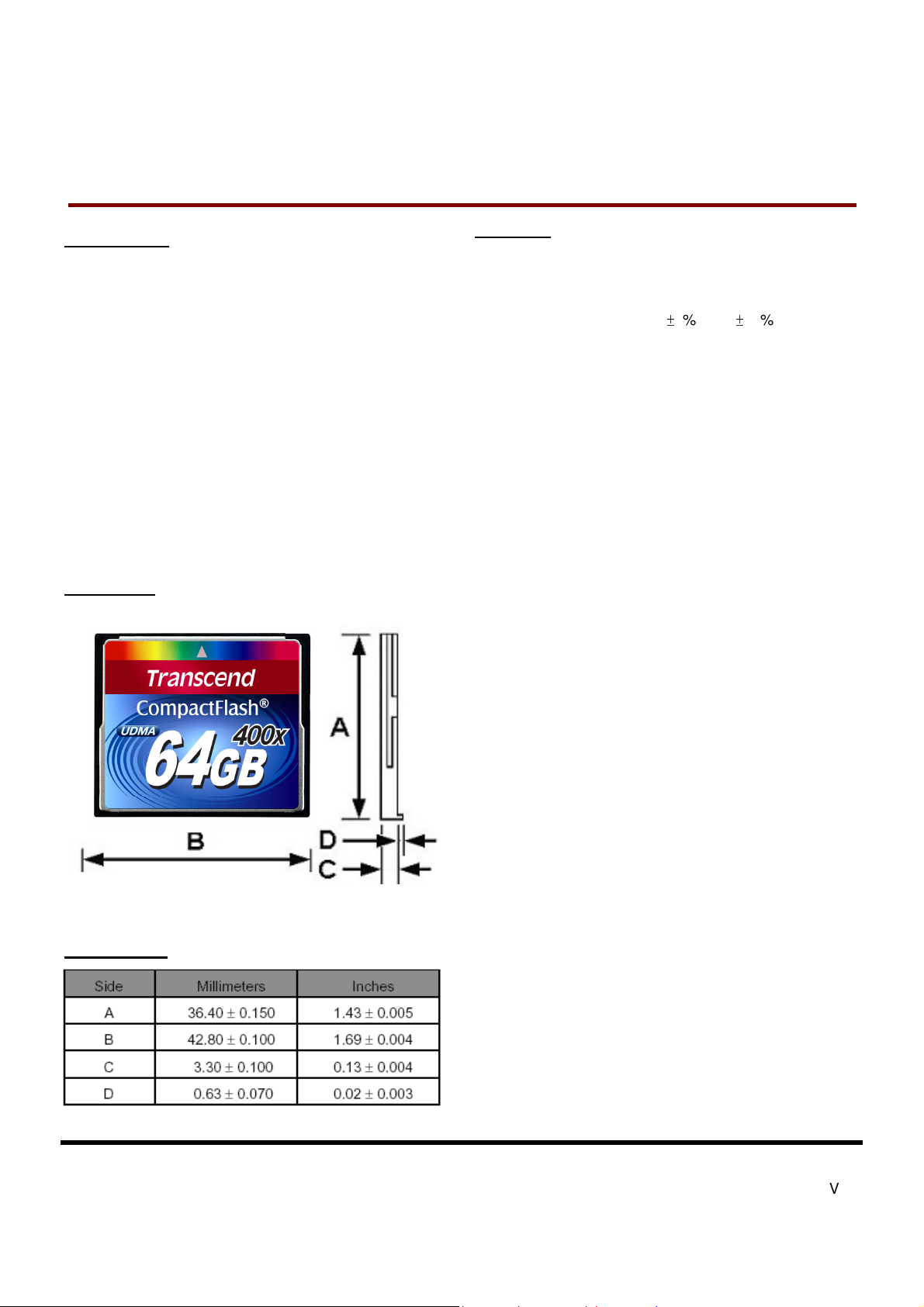
Dimensions
Transcend Information Inc.
•
True IDE mode: Fixed Disk (Default)
•
PC Card Mode: Removable Disk (Default)
• Durability of Connector: 10,000 times
• Built-in 15 bit ECC (Error Correction Code) functionality
• Support Global Wear-Leveling to extend product life
• Transfer rate up to read 90MB/s write 60MB/s based on
TestMetrix.
V1.0
Page 2
T
2
S
1
6
G
~
6
4
G
C
F
T
S
1
6
G
~
6
4
T
S
1
6
G
Specification
Interface Specification
Drivers
ATA Compatibility
Physical Specification
~
6
4
G
G
C
C
F
F
4
4
4
0
0
0
0
0
0
No Device Driver Required
ATA/ATAPI 7
PIO Mode 0 - 6
Multiword mode 0 - 4
UDMA Mode 0 - 6
400X CompactFlash Card
Form Factor
Storage Capacities
Dimensions (mm)
Environmental Specifications
Operating Temperature
Storage Temperature
Humidity
Operating Humidity (Non condensation)
Storage Humidity (Non condensation)
* Note: 24-hours chamber test on ASUS Striker 2 Extreme, 1GB RAM, Windows® XP Version 2002 SP3.
Length
Width
Height
Compact Flash Card
16 GB to 64 GB
36.40 ± 0.15
42.80 ± 0.10
3.30 ± 0.10
-25 ℃ to 85 ℃
-40 ℃ to 85 ℃
5% to 95%
5% to 95%
Power Consumption
Product
Power
Consumption
(DC 3.3V @25℃)
Transcend Information Inc.
Standby
Read
Write
TS16GF400 TS32GCF400 TS64GCF400
0.2mA 0.2mA 0.2mA
221.0mA 225.7mA
213.2mA 231.7mA
231.6mA
205.7mA
V1.0
Page 3
T
3
T
T
S
S
S
1
1
1
6
6
6
G
G
G
~
~
~
6
6
6
4
4
4
G
G
G
C
C
C
F
F
F
4
4
4
0
0
0
0
0
0
400X CompactFlash Card
Performance
TS16GCF400 16GB 83.67 44.96 82.38 8.671
TS32GCF400 32GB 86.16 45.82 85.09 10.99
TS64GCF400 64GB 88.87 39.67 88.48 10.59
Note : 25 ℃, according to IDE to CF card transferring board test on ASUS P4S800-MX, 1GB RAM, IDE interface support
UDMA6, Windows® XP Version 2002 SP2, CrystalDiskMark, copied file 100MB
Actual Capacity
* Note: FAT32 format
Model P/N Capacity Read(MB/s) Write(MB/s) Random Read (MB/s) Random Write (MB/s)
Model P/N User LBA Cylinder Head Sector
TS16GCF400 31293360 31045 16 63
TS32GCF400 62537328 62041 16 63
TS64GCF400 125059072 16383 15 63
Transcend Information Inc.
Transcend
V1.0
Page 4

T
4
S
1
6
G
~
6
4
T
S
1
6
S
1
6
G
G
T
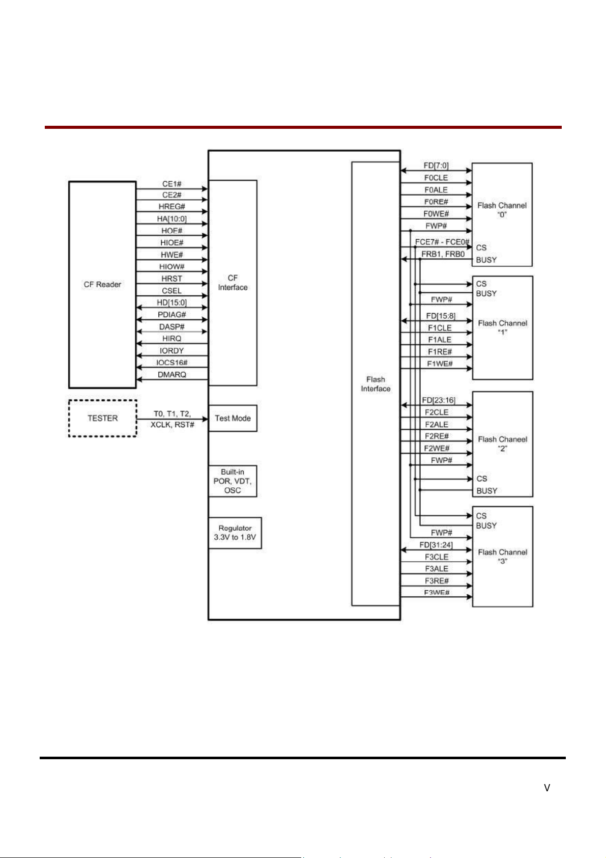
Block Diagram
~
~
6
6
4
4
G
G
G
C
C
C
F
F
F
4
4
4
0
0
0
0
0
0
400X CompactFlash Card
Transcend Information Inc.
V1.0
Page 5
T
5
T
T
S
S
S
1
1
1
6
6
6
G
G
G
~
~
~
6
6
6
4
4
4
G
G
G
C
C
C
F
F
F
4
4
4
0
0
0
0
0
0
400X CompactFlash Card
Transcend Information Inc.
V1.0
Page 6

T
6
S
1
6
G
~
6
4
G
C
F
4
0
0
4
4
0
0
0
0
T
T
S
S
1
1
6
6
G
G
~
~
6
6
4
4
G
G
C
C
F
F
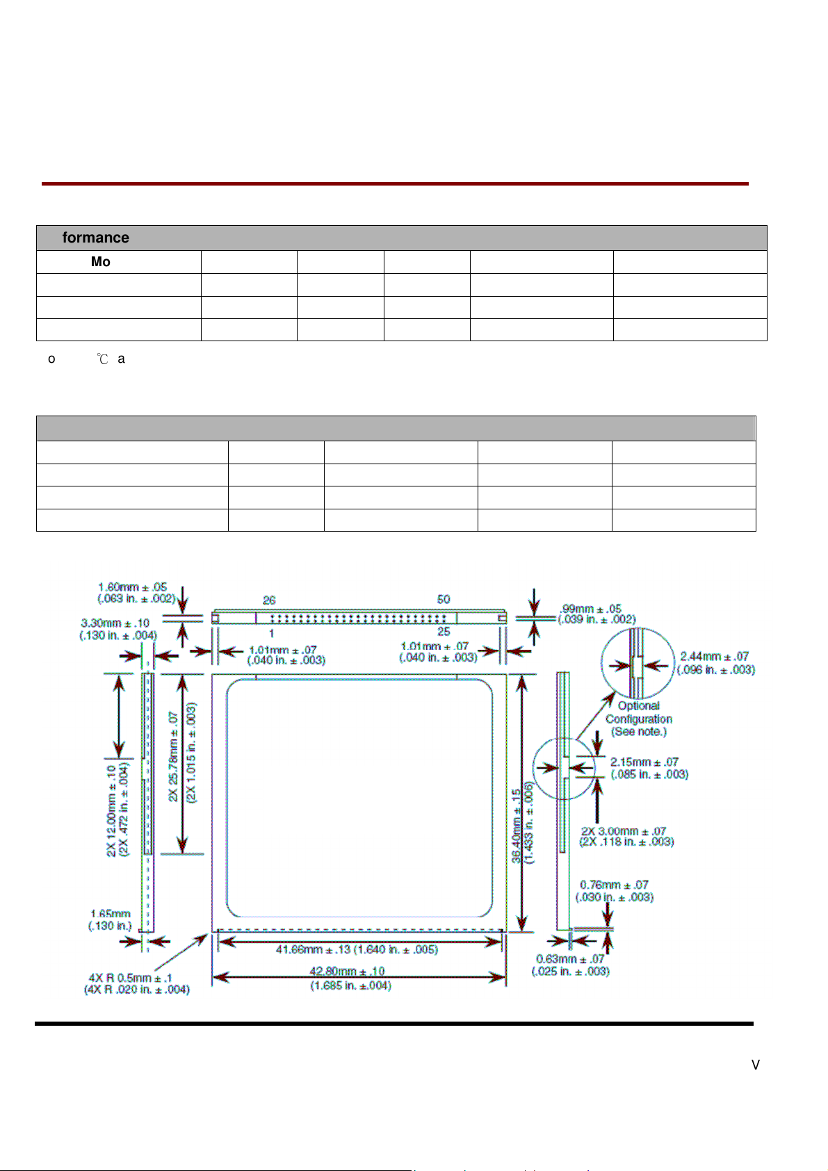
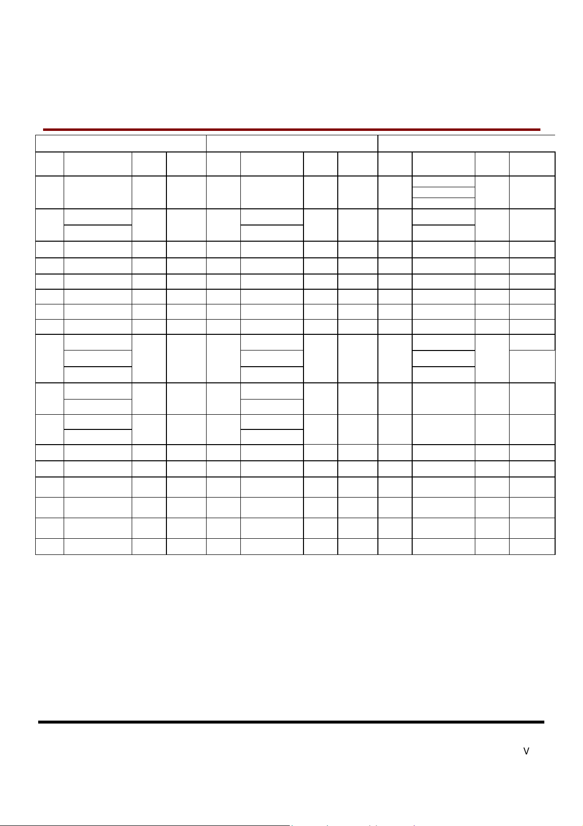
Pin Assignments and Pin Type
400X CompactFlash Card
PC Card Memory Mode PC Card I/O Mode True IDE Mode
Pin
Num
1 GND
2 D03 I/O I1Z, OZ3 2 D03 I/O I1Z, OZ3
3 D04 I/O I1Z, OZ3 3 D04 I/O I1Z, OZ3
4 D05 I/O I1Z, OZ3 4 D05 I/O I1Z, OZ3
5 D06 I/O I1Z, OZ3 5 D06 I/O I1Z, OZ3
6 D07 I/O I1Z, OZ3 6 D07 I/O I1Z, OZ3
7 -CE1 I I3U 7 -CE1 I I3U 7 -CS0 I I3Z
8 A10 I I1Z 8 A10 I I1Z 8 A102 I I1Z
9 -OE I I3U 9 -OE I I3U 9 -ATA SEL
10
11
12
13
14
15
16
17
18
19
20
21
22
23
24
25
26
27
28
29
30
31
32
33
Signal
Name
A09 I I1Z 10 A09 I I1Z 10 A092 I I1Z
A08 I I1Z 11 A08 I I1Z 11 A082 I I1Z
A07 I I1Z 12 A07 I I1Z 12 A072 I I1Z
VCC
A06 I I1Z 14 A06 I I1Z 14 A062 I I1Z
A05 I I1Z 15 A05 I I1Z 15 A052 I I1Z
A04 I I1Z 16 A04 I I1Z 16 A042 I I1Z
A03 I I1Z 17 A03 I I1Z 17 A032 I I1Z
A02 I I1Z 18 A02 I I1Z 18 A02 I I1Z
A01 I I1Z 19 A01 I I1Z 19 A01 I I1Z
A00 I I1Z 20 A00 I I1Z 20 A00 I I1Z
D00 I/O I1Z, OZ3 21 D00 I/O I1Z, OZ3 21 D00 I/O I1Z, OZ3
D01 I/O I1Z, OZ3 22 D01 I/O I1Z, OZ3 22 D01 I/O I1Z, OZ3
D02 I/O I1Z, OZ3 23 D02 I/O I1Z, OZ3 23 D02 I/O I1Z, OZ3
WP O OT3 24 -IOIS16 O OT3 24 -IOCS16
-CD2 O Ground 25 -CD2 O Ground
-CD1 O Ground 26 -CD1 O Ground
D111 I/O I1Z, OZ3 27 D111 I/O I1Z, OZ3 27 D111 I/O I1Z, OZ3
D121 I/O I1Z, OZ3 28 D121 I/O I1Z, OZ3 28 D121 I/O I1Z, OZ3
D131 I/O I1Z, OZ3 29 D131 I/O I1Z, OZ3 29 D131 I/O I1Z, OZ3
D141 I/O I1Z, OZ3 30 D141 I/O I1Z, OZ3 30 D141 I/O I1Z, OZ3
D151 I/O I1Z, OZ3 31 D151 I/O I1Z, OZ3 31 D151 I/O I1Z, OZ3
-CE21 I I3U 32 -CE21 I I3U 32 -CS11 I I3Z
-VS1 O Ground 33 -VS1 O Ground
Pin
Type
In, Out Type Pin Num
Ground 1 GND
Power 13 VCC
Signal
Name
Pin
Type
In, Out
Type
Ground
Power
Pin
Num
1 GND
2 D03 I/O I1Z, OZ3
3 D04 I/O I1Z, OZ3
4 D05 I/O I1Z, OZ3
5 D06 I/O I1Z, OZ3
6 D07 I/O I1Z, OZ3
13 VCC
25 -CD2 O Ground
26 -CD1 O Ground
33 -VS1 O Ground
Signal
Name
4
Pin
Type
O ON3
In, Out
Type
Ground
I I3U
Power
Transcend Information Inc.
V1.0
Page 7
T
7
S
T
S
T
S
Pin
Num
34
35
36
37
38
39
40
41
42
43
44
45
46
47
48
49
50
1
6
G
~
6
4
G
C
F
4
0
0
1
6
G
~
6
4
G
C
1
6
G
~
6
4
PC Card Memory Mode PC Card I/O Mode True IDE Mode
Signal Name
-HIOE
HSTROBE
HDMARDY
-IOWR -IOWR -IOWR7
10,11
STOP
-WE I I3U 36 -WE I I3U 36 -WE3 I I3U
READY O OT1 37 -IREQ O OT1 37 INTRQ O OZ1
VCC Power 38 VCC Power 38 VCC Power
-CSEL5 I I2Z 39 -CSEL5 I I2Z 39 -CSEL I I2U
-VS2 O OPEN 40 -VS2 O OPEN 40 -VS2 O OPEN
RESET I I2Z 41 RESET I I2Z 41 -RESET I I2Z
-WAIT -WAIT IORDY7 ON1
-DDMARDY
DSTROBE11
-INPACK -INPACK
-DMARQ12
-REG I I3U 44 -REG
-DMACK
BVD2 O OT1 45 -SPKR O OT1 45 -DASP I/O I1U, ON1
BVD1 O OT1 46 -STSCHG O OT1 46 -PDIAG I/O I1U, ON1
D081 I/O
D091 I/O
D101 I/O
GND Ground 50 GND Ground 50 GND Ground
F
G
C
F
Pin
Type
10
11
10
12
DMACK
4
0
0
4
0
0
In, Out
Type
I I3U 34
I I3U 35
O OT1 42
O OT1 43
I1Z,
OZ3
I1Z,
OZ3
I1Z,
OZ3
Pin
Num
47 D081 I/O
48 D091 I/O
49 D101 I/O
Signal Name
-HIOE
HSTROBE10
-HDMARDY11
10,11
STOP
-DDMARDY10
DSTROBE
-DMARQ12
12
11
400X CompactFlash Card
Pin
Type
In, Out
Type
I I3U 34
I I3U 35
O OT1 42
O OT1 43 DMARQ O OZ1
I I3U 44 -DMACK 6 I I3U
I1Z,
OZ3
I1Z,
OZ3
I1Z,
OZ3
Pin
Num
Signal Name
-HIOE7
HSTROBE8
-HDMARDY
8,9
STOP
-DDMARDY8
DSTROBE9
47 D081 I/O I1Z, OZ3
48 D091 I/O I1Z, OZ3
49 D101 I/O I1Z, OZ3
Pin
Type
I I3Z
9
I I3Z
O
4
In, Out
Type
OT113
Note: 1) These signals are required only for 16 bit accesses and not required when installed in 8 bit systems. Devices should allow for 3-state
signals not to consume current.
2) The signal should be grounded by the host.
3) The signal should be tied to VCC by the host.
4) The mode is required for CompactFlash Storage Cards.
5) The -CSEL signal is ignored by the card in PC Card modes. However, because it is not pulled upon the card in these modes,
it should not be left floating by the host in PC Card modes. In these modes, the pin should be connected by the host to PC
Card A25 or grounded by the host.
6) If DMA operations are not used, the signal should be held high or tied to VCC by the host. For proper operation in older hosts: while DMA
operations are not active, the card shall ignore this signal,including a floating condition
7) Signal usage in True IDE Mode except when Ultra DMA mode protocol is active.
8) Signal usage in True IDE Mode when Ultra DMA mode protocol DMA Write is active.
9) Signal usage in True IDE Mode when Ultra DMA mode protocol DMA Read is active.
10) Signal usage in PC Card I/O and Memory Mode when Ultra DMA mode protocol DMA Write is active.
11) Signal usage in PC Card I/O and Memory Mode when Ultra DMA mode protocol DMA Read is active.
12) Signal usage in PC Card I/O and Memory Mode when Ultra DMA protocol is active.
Transcend Information Inc.
V1.0
Page 8
T
8
T
T
S
S
S
1
1
1
6
6
6
G
G
G
~
~
~
6
6
6
4
4
4
G
G
G
C
C
C
F
F
F
4
4
4
0
0
0
0
0
0
400X CompactFlash Card
Input Leakage Current
Note: In Table 1 below, x refers to the characteristics described in table 2. For example, I1U indicates a pull-up resistor with a type 1
input characteristic.
Type Parameter Symbol
IxZ Input Leakage Current
IxU Pull-Up Resistor RPU1 Vcc = 5.0V 50k
IxD Pull-Down Resistor RPD1 Vcc = 5.0V 50k
Note: The minimum pull-up resistor resistance meets the PCMCIA PC Card specification of 10k ohms but is intentionally higher in the
CompactFlash Specification to reduce power use.
Input Characteristics
Type Parameter Symbol
Input Voltage
1
CMOS
Input Voltage
2
CMOS
Input Voltage
3
CMOS Schmitt
Trigger
Notes: 1) The host provides a logic output high voltage for a CMOS load of .9 x VCC. For a 5 volt product, this translates to .9 x
4.5 = 4.05 volts minimum Voh.
Table 1: Input Leakage Current
Conditions MIN TYP MAX Units
IL Vih = Vcc / Vil = Gnd -1
500k Ohm
500k Ohm
1 µA
Table 2: Input Characteristics
Units
Volts
Volts
Volts
Vih
Vil
Vih
Vil
Vth
Vtl
MIN TYP MAX MIN TYP MAX
VCC = 3.3 V VCC = 5.0 V
2.4
1.5
1.8
1.0
0.6 4.0
0.6 2.0
1
2.8
2.0
0.8
0.8
Output Drive Type
Note: In Table 3 below, x refers to the characteristics described in Table 4. For example, OT3 refers to Totem pole output with a type
3 output drive characteristic.
Type Output Type Valid Conditions
OTx Totempole Ioh & Iol
OZx Tri-State N-P Channel Ioh & Iol
OPx P-Channel Only Ioh Only
ONx N-Channel Only Iol Only
Transcend Information Inc.
Table 3: Output Drive Type
V1.0
Page 9

T
9
S
1
6
G
~
6
4
G
C
F
4
T
S
1
6
G
~
6
4
T
S
1
6
G
Output Drive Characteristics
Type
1 Output Voltage
2 Output Voltage
3 Output Voltage
X
G
~
6
4
G
Parameter Symbol Conditions MIN TYP MAX Units
Tri-State Leakage
C
F
4
C
F
4
Current
0
0
0
0
0
0
Table 4: Output Drive Characteristics
Voh
Vol
Voh
Vol
Voh
Vol
Ioz
Ioh = -4 mA
Iol = 4 mA
Ioh = -4 mA
Iol = 4 mA
Ioh = -4 mA
Iol = 4 mA
Vol = Gnd
Voh = Vcc
Vcc
-0.8V
Vcc
-0.8V
Vcc
-0.8V
-10
400X CompactFlash Card
Gnd
+0.4V
Gnd
+0.4V
Gnd
+0.4V
10 µA
Volts
Volts
Volts
Transcend Information Inc.
V1.0
Page 10

T
10
select the following:
port address registers within the CompactFlash Storage Card,
tion control and status
READY and Write
Present signal in
CompactFlash Storage
S
1
6
G
~
6
4
G
6
6
4
4
G
G
C
C
C
T
T
S
S
1
1
6
6
G
G
~
~
Signal Description
F
F
F
4
4
4
0
0
0
0
0
0
400X CompactFlash Card
Signal Name
A10 – A00
(PC Card Memory Mode)
A10 – A00
(PC Card I/O Mode)
A02 - A00
(True IDE Mode)
BVD1
(PC Card Memory Mode)
-STSCHG
(PC Card I/O Mode)
Status Changed
-PDIAG
(True IDE Mode)
BVD2
(PC Card Memory Mode)
-SPKR
(PC Card I/O Mode)
-DASP
(True IDE Mode)
Dir.
I
I
I/O
I/O
Pin
8,10,11,12,
14,15,16,17,
18,19,20
18,19,20
46 This signal is asserted high, as BVD1 is not supported.
45 This signal is asserted high, as BVD2 is not supported.
These address lines along with the -REG signal are used to
The I/O port address registers within the CompactFlash Storage Card , the
memory mapped
a byte in the card's information structure and its configura
registers.
This signal is the same as the PC Card Memory Mode signal.
In True IDE Mode, only A[02:00] are used to select the one of eight registers
in the Task File, the remaining address lines should be grounded by the
host.
This signal is asserted low to alert the host to changes in the
Protect states, while the I/O interface is configured. Its use is controlled by the
Card Config and Status Register.
In the True IDE Mode, this input / output is the Pass Diagnostic signal in the
Master / Slave handshake protocol.
This line is the Binary Audio output from the card. If the Card does not support
the Binary Audio function, this line should be held negated.
In the True IDE Mode, this input/output is the Disk Active/Slave
the Master/Slave handshake protocol.
Description
-CD1, -CD2
(PC Card Memory Mode)
-CD1, -CD2
(PC Card I/O Mode)
-CD1, -CD2
(True IDE Mode)
O
26,25 These Card Detect pins are connected to ground on the
Transcend Information Inc.
Card. They are used by the host to determine that the CompactFlash Storage
Card is fully inserted into its socket.
This signal is the same for all modes.
This signal is the same for all modes.
V1.0
Page 11

T
11
the host to PC
the host to PC
a Master or a
between the host
Byte of the Word. D08 is the LSB
on the low order
T
T
S
S
S
1
1
1
6
6
6
G
G
G
~
~
~
6
6
6
4
4
4
G
G
G
C
C
C
F
F
F
4
4
4
0
0
0
0
0
0
400X CompactFlash Card
Signal Name
-CE1, -CE2
(PC Card Memory Mode)
Card Enable
-CE1, -CE2
(PC Card I/O Mode)
Card Enable
-CS0, -CS1
(True IDE Mode)
-CSEL
(PC Card Memory Mode)
-CSEL
(PC Card I/O Mode)
-CSEL
(True IDE Mode)
Dir.
I
I
Pin
7,32
39
These input signals are used both to select the card and to indicate to the card
whether a byte or a word operation is being performed. -CE2 always accesses
the odd byte of the word.-CE1 accesses the even byte or the Odd byte of the
word depending on A0 and -CE2. A multiplexing scheme based on A0,-CE1,
-CE2 allows 8 bit hosts to access all data on D0-D7. See Table 27, Table 29,
Table 31, Table 35, Table 36 and Table 37.
This signal is the same as the PC Card Memory Mode signal.
In the True IDE Mode, -CS0 is the address range select for the task file
registers while -CS1 is used to select the Alternate Status Register and the
Device Control Register.
While –DMACK is asserted, -CS0 and –CS1 shall be held negated and the
width of the transfers shall be 16 bits.
This signal is not used for this mode, but should be connected by
Card A25 or grounded by the host.
This signal is not used for this mode, but should be connected by
Card A25 or grounded by the host.
This internally pulled up signal is used to configure this device as
Slave when configured in the True IDE Mode.
Description
D15 - D00
(PC Card Memory Mode)
D15 - D00
(PC Card I/O Mode)
D15 - D00
(True IDE Mode)
GND
(PC Card Memory Mode)
GND
(PC Card I/O Mode)
GND
(True IDE Mode)
I/O
--
Transcend Information Inc.
31,30,29,28,
27,49,48,47,
6,5,4,3,2,
23, 22, 21
1,50 Ground.
When this pin is grounded, this device is configured as a Master.
When the pin is open, this device is configured as a Slave.
These lines carry the Data, Commands and Status information
and the controller. D00 is the LSB of the Even
of the Odd Byte of the Word.
This signal is the same as the PC Card Memory Mode signal.
In True IDE Mode, all Task File operations occur in byte mode
bus D[7:0] while all data transfers are 16 bit using D[15:0].
This signal is the same for all modes.
This signal is the same for all modes.
V1.0
Page 12

T
12
of
transfers between host
device when it is ready to transfer data to
handshake manner with
while the host is
is not selected in
PC Card and True
gates I/O data onto
Card when the card is configured to use
signal has the same
signal is asserted
in bursts.
rising and falling edge of HSTROBE
T
T
S
S
S
1
6
G
~
1
6
G
~
1
6
G
~
Signal Name
6
6
6
4
4
4
G
G
G
C
C
C
F
F
F
4
4
4
0
0
0
0
0
0
Dir.
Pin
Description
400X CompactFlash Card
-INPACK
(PC Card Memory Mode except
Ultra DMA Protocol Active)
-INPACK
(PC Card I/O Mode except Ultra
DMA Protocol Active)
Input Acknowledge
-DMARQ
(PC Card Memory Mode -Ultra
DMA Protocol Active)
-DMARQ
(PC Card I/O Mode -Ultra DMA
Protocol Active)
DMARQ
(True IDE Mode)
-HIOE
(PC Card Memory Mode except
Ultra DMA Protocol Active)
-HIOE
(PC Card I/O Mode except Ultra
DMA Protocol Active)
-HIOE
(True IDE Mode – Except Ultra
DMA Protocol Active)
-HDMARDY
(All Modes - Ultra DMA Protocol
DMA Read)
HSTROBE
(All Modes - Ultra DMA Protocol
DMA Write)
O
I
43 This signal is not used in this mode.
The Input Acknowledge signal is asserted by the CompactFlash Storage Card
when the card is selected and responding to an I/O read cycle at the address
that is on the address bus. This signal is used by the host to control the enable
any input data buffers between the CompactFlash Storage Card and the CPU.
Hosts that support a single socket per interface logic, such as for Advanced
Timing Modes and Ultra DMA operation may ignore the –INPACK signal from
the device and manage their input buffers based solely on Card Enable signals.
This signal is a DMA Request that is used for DMA data
and device. It shall be asserted by the
or from the host. For Multiword DMA transfers, the direction of data transfer is
controlled by -HIOE and -IOWR. This signal is used in a
(-)DMACK, i.e., the device shall wait until the host asserts (-)DMACK before
negating (-)DMARQ, and re-asserting (-)DMARQ if there is more data to
transfer.
In PCMCIA I/O Mode, the -DMARQ shall be ignored by the host
performing an I/O Read cycle to the device. The host shall not initiate an I/O
Read cycle while -DMARQ is asserted by the device.
In True IDE Mode, DMARQ shall not be driven when the device
the Drive-Head register.
While a DMA operation is in progress, -CS0 (-CE1)and -CS1 (-CE2) shall be
held negated and the width of the transfers shall be 16 bits.
If there is no hardware support for True IDE DMA mode in the host, this output
signal is not used and should not be connected at the host. In this case, the
BIOS must report that DMA mode is not supported by the host so that device
drivers will not attempt DMA mode operation.
A host that does not support DMA mode and implements both
IDE modes of operation need not alter the PC Card mode connections while in
True IDE mode as long as this does not prevent proper operation in any mode.
34 This signal is not used in this mode.
This is an I/O Read strobe generated by the host. This signal
the bus from the CompactFlash Storage
the I/O interface.
In True IDE Mode, while Ultra DMA mode is not active, this
function as in PC Card I/O Mode.
In all modes when Ultra DMA mode DMA Read is active, this
by the host to indicate that the host is ready to receive Ultra DMA dataThe host may negate – HDMARDY to pause an Ultra DMA transfer.
In all modes when Ultra DMA mode DMA Write is active, this signal is the data
out strobe generated by the host. Both the
cause data to be latched by the device. The host may stop generating
HSTROBE edges to pause an Ultra DMA data-out burst.
Transcend Information Inc.
V1.0
Page 13

T
13
Except Ultra
assertion of this signal
is
continuous assertion of RESET from the application
Interrupt Request. This line is
S
1
6
G
~
6
4
G
C
T
S
1
6
G
~
6
T
S
1
6
Signal Name
-IOWR
(PC Card Memory Mode– Except
Ultra DMA Protocol Active)
-IOWR
(PC Card I/O Mode –
DMA Protocol Active)
-IOWR
(True IDE Mode – Except Ultra
DMA Protocol Active)
STOP
(All Modes – Ultra DMA Protocol
Active)
-OE
(PC Card Memory Mode)
-OE
(PC Card I/O Mode)
-ATA SEL
(True IDE Mode)
READY
(PC Card Memory Mode)
-IREQ
(PC Card I/O Mode)
INTRQ
(True IDE Mode)
G
~
4
6
4
G
G
C
C
F
F
F
4
4
4
0
0
0
0
0
0
Dir.
I
I
O
Pin
35
9
37
This signal is not used in this mode.
The I/O Write strobe pulse is used to clock I/O data on the Card Data bus into
the CompactFlash Storage Card controller registers when the CompactFlash
Storage Card is configured to use the I/O interface.
The clocking shall occur on the negative to positive edge of the signal (trailing
edge).
In True IDE Mode, while Ultra DMA mode protocol is not active, this signal has
the same function as in PC Card I/O Mode. When Ultra DMA mode protocol is
supported, this signal must be negated before entering Ultra DMA mode
protocol.
In All Modes, while Ultra DMA mode protocol is active, the
causes the termination of the Ultra DMA data burst.
This is an Output Enable strobe generated by the host interface. It is used to
read data from the CompactFlash Storage Card in Memory Mode and to read
the CIS and configuration registers.
In PC Card I/O Mode, this signal is used to read the CIS and configuration
registers.
To enable True IDE Mode this input should be grounded by the host.
In Memory Mode, this signal is set high when the CompactFlash Storage Card
ready to accept a new data transfer operation and is held low when the card is
busy.
At power up and at Reset, the READY signal is held low (busy) until the
CompactFlash Storage Card has completed its power up or reset function. No
access of any type should be made to the CompactFlash Storage Card during
this time.
Note, however, that when a card is powered up and used with RESET
continuously disconnected or asserted, the Reset function of the RESET pin is
disabled. Consequently, the
of power shall not cause the READY signal to remain continuously in the busy
state.
I/O Operation – After the CompactFlash Storage Card Card has been
configured for I/O operation, this signal is used as strobed low to generate a pulse mode interrupt or held low for a level mode
interrupt.
In True IDE Mode signal is the active high Interrupt Request to the host.
Description
400X CompactFlash Card
Transcend Information Inc.
V1.0
Page 14

T
14
Except Ultra
High for Common Memory,
protocol on the card the, host shall keep the
I/O address is on
the host and the
REG
shall ignore the
RESET pin is high with the
S
1
6
G
~
6
4
G
C
T
S
1
6
G
~
6
T
S
1
6
Signal Name
-REG
(PC Card Memory Mode– Except
Ultra DMA Protocol Active)
Attribute Memory Select
-REG
(PC Card I/O Mode –
DMA Protocol Active)
-DMACK
(PC Card Memory Mode when
Ultra DMA Protocol Active)
DMACK
(PC Card I/O Mode when Ultra
DMA Protocol Active)
-DMACK
(True IDE Mode)
G
~
6
4
4
G
G
C
C
F
F
F
4
4
4
0
0
0
0
0
0
Dir.
I
Pin
44
This signal is used during Memory Cycles to distinguish between Common
Memory and Register (Attribute) Memory accesses.
Low for Attribute Memory.
In PC Card Memory Mode, when Ultra DMA Protocol is supported by the host
and the host has enabled Ultra DMA
-REG signal negated during the execution of any DMA Command by the device.
The signal shall also be active (low) during I/O Cycles when the
the Bus.
In PC Card I/O Mode, when Ultra DMA Protocol is supported by
host has enabled Ultra DMA protocol on the card the, host shall keep the signal asserted during the execution of any DMA Command by the device.
This is a DMA Acknowledge signal that is asserted by the host in response to
(-)DMARQ to initiate DMA transfers.
In True IDE Mode, while DMA operations are not active, the card
(-)DMACK signal, including a floating condition.
If DMA operation is not supported by a True IDE Mode only host, this signal
should be driven high or connected to VCC by the host.
A host that does not support DMA mode and implements both PC Card and
True-IDE modes of operation need not alter the PC Card mode connections
while in True-IDE mode as long as this does not prevent proper operation all
modes.
Description
400X CompactFlash Card
RESET
(PC Card Memory Mode)
RESET
(PC Card I/O Mode)
-RESET
(True IDE Mode)
VCC
(PC Card Memory Mode)
VCC
(PC Card I/O Mode)
VCC
(True IDE Mode)
--
I
41 The CompactFlash Storage Card is Reset when the
following important exception:
The host may leave the RESET pin open or keep it continually high from the
application of power without causing a continuous Reset of the card. Under
either of these conditions, the card shall emerge from power-up having
completed an initial Reset.
The CompactFlash Storage Card is also Reset when the Soft Reset bit in the
Card Configuration Option Register is set.
This signal is the same as the PC Card Memory Mode signal.
In the True IDE Mode, this input pin is the active low hardware reset from the
host.
13,38 +5 V, +3.3 V power.
This signal is the same for all modes.
This signal is the same for all modes.
Transcend Information Inc.
V1.0
Page 15

T
15
VS2 is
Except
Except Ultra
Card to signal the
signal is asserted
signal is the data in
write data to the
registers of the CompactFlash Storage Card when the card is configured in the
connected to VCC
does not have a write protect
IOIS16) function. A
that a 16 bit or odd byte only operation can be performed at
device is expecting
S
1
6
G
~
6
4
G
C
T
S
1
6
G
~
6
T
S
1
6
Signal Name
-VS1
-VS2
(PC Card Memory Mode)
-VS1
-VS2
(PC Card I/O Mode)
-VS1
-VS2
(True IDE Mode)
-WAIT
(PC Card Memory Mode –
Ultra DMA Protocol Active)
-WAIT
(PC Card I/O Mode –
DMA Protocol Active)
IORDY
(True IDE Mode – Except Ultra
DMA Protocol Active)
-DDMARDY
(All Modes – Ultra DMA Write
Protocol Active)
DSTROBE
(All Modes – Ultra DMA Read
Protocol Active)
G
~
4
6
4
G
G
C
C
F
F
F
4
4
4
0
0
0
0
0
0
Dir.
O
O
Pin
33
40
42
Voltage Sense Signals. -VS1 is grounded on the Card and sensed by the Host
so that the CompactFlash Storage Card CIS can be read at 3.3 volts and reserved by PCMCIA for a secondary voltage and is not connected on the Card.
This signal is the same for all modes.
This signal is the same for all modes.
The -WAIT signal is driven low by the CompactFlash Storage
host to delay completion of a memory or I/O cycle that is in progress.
This signal is the same as the PC Card Memory Mode signal.
In True IDE Mode, except in Ultra DMA modes, this output signal may be used
as IORDY.
In all modes, when Ultra DMA mode DMA Write is active, this
by the device during a data burst to indicate that the device is ready to receive
Ultra DMA data out bursts. The device may negate -DDMARDY to pause an
Ultra DMA transfer.
In all modes, when Ultra DMA mode DMA Read is active, this
strobe generated by the device. Both the rising and falling edge of DSTROBE
cause data to be latched by the host. The device may stop generating
DSTROBE edges to pause an Ultra DMA data in burst.
Description
400X CompactFlash Card
-WE
(PC Card Memory Mode)
-WE
(PC Card I/O Mode)
-WE
(True IDE Mode)
WP
(PC Card Memory Mode)
Write Protect
-IOIS16
(PC Card I/O Mode)
-IOCS16
(True IDE Mode)
I
O
Transcend Information Inc.
36 This is a signal driven by the host and used for strobing memory
memory interface mode. It is also used for writing the configuration registers.
In PC Card I/O Mode, this signal is used for writing the configuration registers.
In True IDE Mode, this input signal is not used and should be
by the host.
24
Memory Mode – The CompactFlash Storage Card
switch. This signal is held low after the completion of the reset initialization
sequence.
I/O Operation – When the CompactFlash Storage Card is configured for I/O
Operation Pin 24 is used for the -I/O Selected is 16 Bit Port (Low signal indicates
the addressed port.
In True IDE Mode this output signal is asserted low when this
a word data transfer cycle.
V1.0
Page 16
T
16
S
1
6
G
~
6
4
G
C
F
4
0
0
4
4
0
0
0
0
400X CompactFlash Card
T
T
S
S
1
1
6
6
G
G
~
~
6
6
4
4
G
G
C
C
F
F
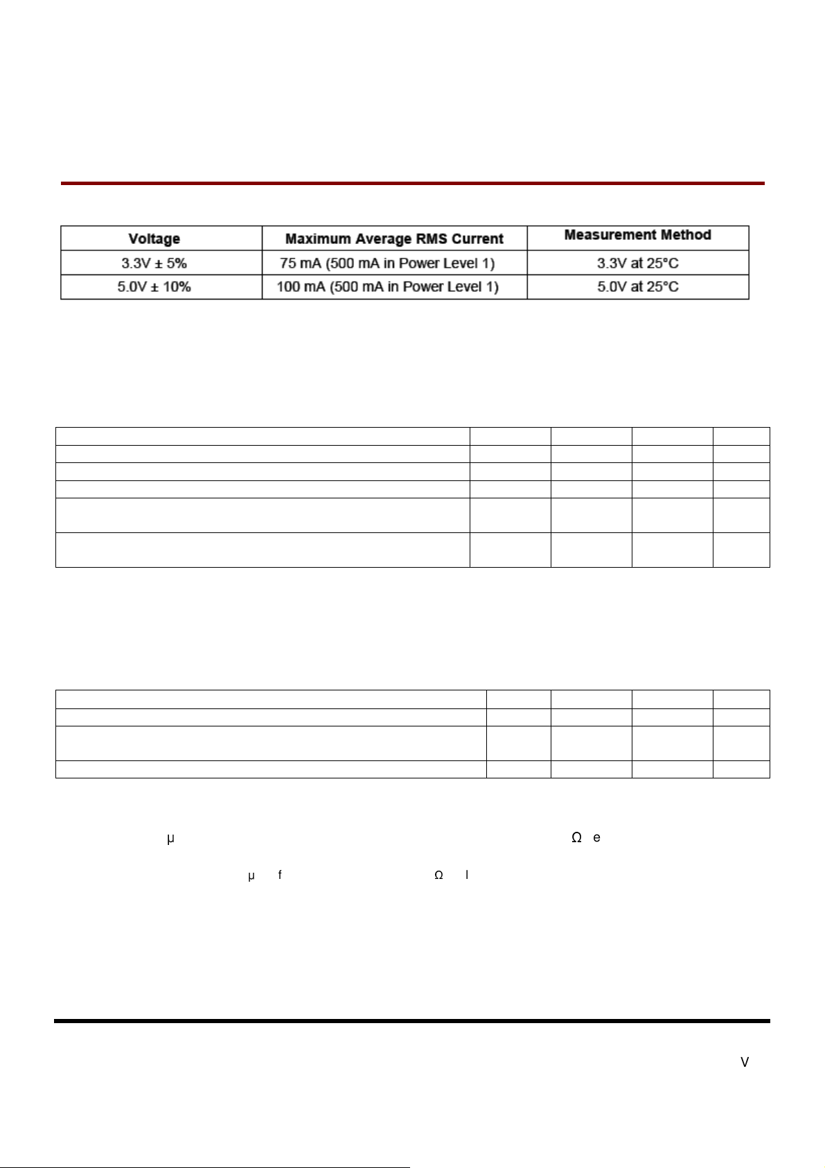
Electrical Specification
The following tables indicate all D.C. Characteristics for the CompactFlash Storage Card. Unless
otherwise stated, conditions are:
Vcc = 5V ±10%
Vcc = 3.3V ± 5%
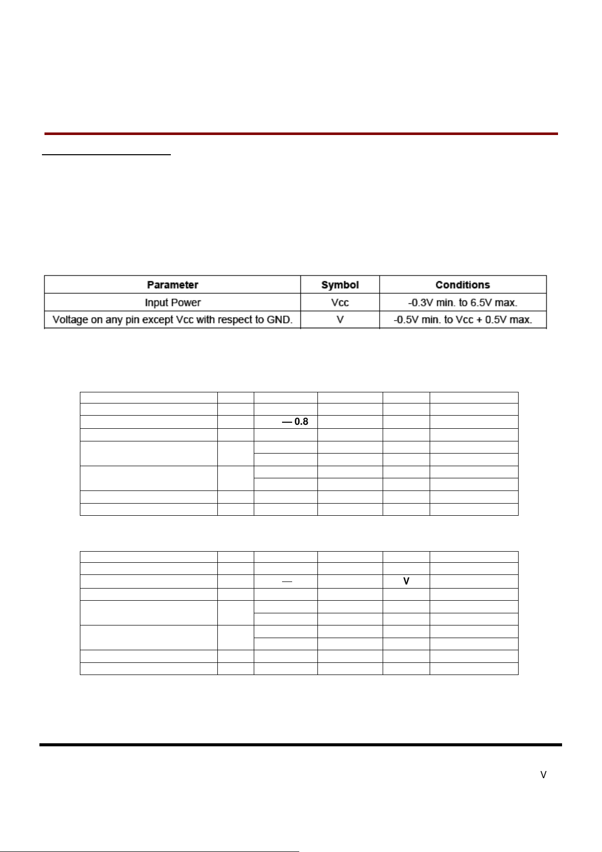
Absolute Maximum Conditions
DC Characteristics
CompactFlash Interface I/O at 5.0V
Parameter
Supply Voltage
High level output voltage VOH
Low level output voltage VOL 0.8 V
High level input voltage VIH
Low level input voltage VIL
Pull up resistance2 RPU 50 73 KOhm
Pull down resistance RPD 50 97 KOhm
CompactFlash Interface I/O at 3.3V
Parameter
Supply Voltage
High level output voltage VOH
Low level output voltage VOL 0.8 V
High level input voltage VIH
Low level input voltage VIL
Pull up resistance2 RPU 52.7 141 KOhm
Pull down resistance RPD 47.5 172 KOhm
1. Include CE1, CE2, HREG, HOE, HIOE, HWE, HIOW pins
2. Include CE1, CE2, HREG, HOE, HIOE, HWE, HIOW, CSEL (P35), PDIAG, DASP pins
Symbol
V
CC
Symbol
V
CC
Min.
4.5 5.5 V
VCC
─
0.8
─
──
4.0 V
2.92 V
0.8 V
1.70 V
Min.
3.135 3.465 V
VCC
────
0.8
2.4 V
2.05 V
0.6 V
1.25 V
Max.
Max.
V
V
Unit
Unit
Remark
Non-schmitt trigger
Schmitt trigger
Non-schmitt trigger
Schmitt trigger
Remark
Non-schmitt trigger
Schmitt trigger
Non-schmitt trigger
Schmitt trigger
1
1
1
1
Transcend Information Inc.
V1.0
Page 17
T
17
hall
S
1
6
G
~
6
4
G
C
F
4
0
0
T
S
1
6
T
S
1
6
Input Power
G
G
~
~
6
6
4
4
G
G
C
F
C
F
4
4
0
0
0
0
400X CompactFlash Card
Input Characteristics for UDMA mode >4
In UDMA modes greater than 4, the following characteristics apply. Voltage output high and low values shall be met
at the source connector to include the effect of series termination.
Table: Input Characteristics (UDMA Mode > 4)
Parameter Symbol MIN MAX Units
DC supply voltage to drivers V
Low to high input threshold V+ 1.5 2.0 Volts
High to low input threshold V- 1.0 1.5 Volts
Difference between input thresholds:
((V+
current value
Average of thresholds:
((V+
current value
) - (V-
) + (V-
current value
current value
))
))/2
V
V
THRAVG
DD3
HYS
3.3 –8% 3.3% + 8% Volts
320 Volts
1.3 1.7 Volts
Output Drive Characteristics for UDMA mode > 4
In UDMA modes greater than 4, the characteristics specified in the following table apply. Voltage output high and low
values shall be met at the source connector to include the effect of series termination.
Table: Output Drive Characteristics (UDMA Mode > 4)
Parameter Symbol
DC supply voltage to drivers V
Voltage output high at -6 mA to +3 mA (at VoH2 the output s
be able to supply and sink current toVDD3)
Voltage output low at 6 mA V
Notes:
oLDASP
1) I
2) I
3) Voltage output high and low values shall be met at the source connector to include the effect of series termination.
4) A device shall have less than 64 μA of leakage current into a 6.2 KΩ pull-down resistor while the INTRQ signal is in the released
state.
shall be 12 mA minimum to meet legacy timing and signal integrity.
oH
value at 400 μA is insufficient in the case of DMARQ that is pulled low by a 5.6 kΩ resistor.
MIN MAX Units
3.3 –8% 3.3% + 8% Volts
DD3
V
V
oH2
0.51 Volts
oL2
–0.51 V
DD3
+0.3 Volts
DD3
Transcend Information Inc.
V1.0
Page 18
T
18
up
S
1
6
G
~
6
4
G
C
F
4
0
0
4
4
0
0
0
0
400X CompactFlash Card
T
T
S
S
1
1
6
6
G
G
~
~
6
6
4
4
G
G
C
C
F
F
Signal Interface
Electrical specifications shall be maintained to ensure data reliability. Additional requirements are necessary for
Advanced Timing Modes and Ultra DMA modes operations. See next sections for additional information.
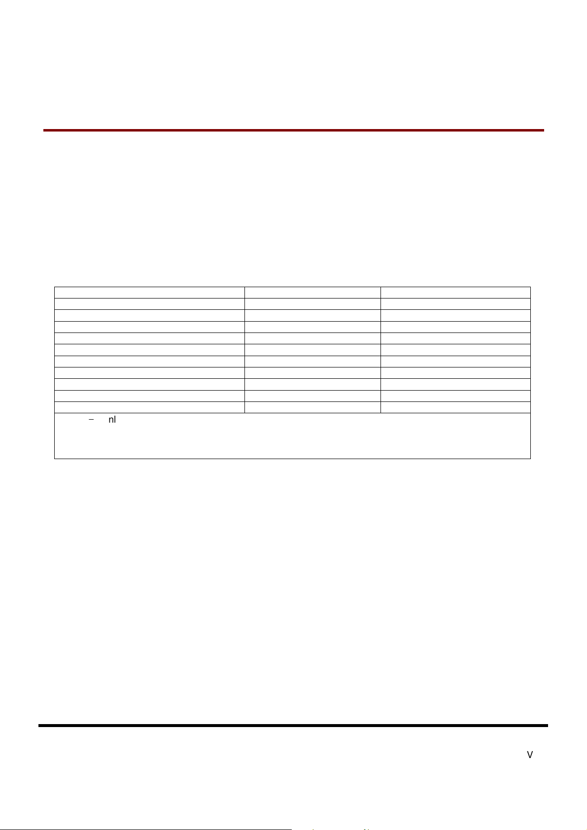
Item Signal Card10 Host
-CE1
-CE2
Control Signal
RESET
Status Signal
-INPACK
-REG
-HIOE
-IOWR
-OE
-WE
READY
-WAIT
WP
Pull-up to VCC 500 K
shall be sufficient to keep inputs inactive
when the pins are not connected at the
1
host.
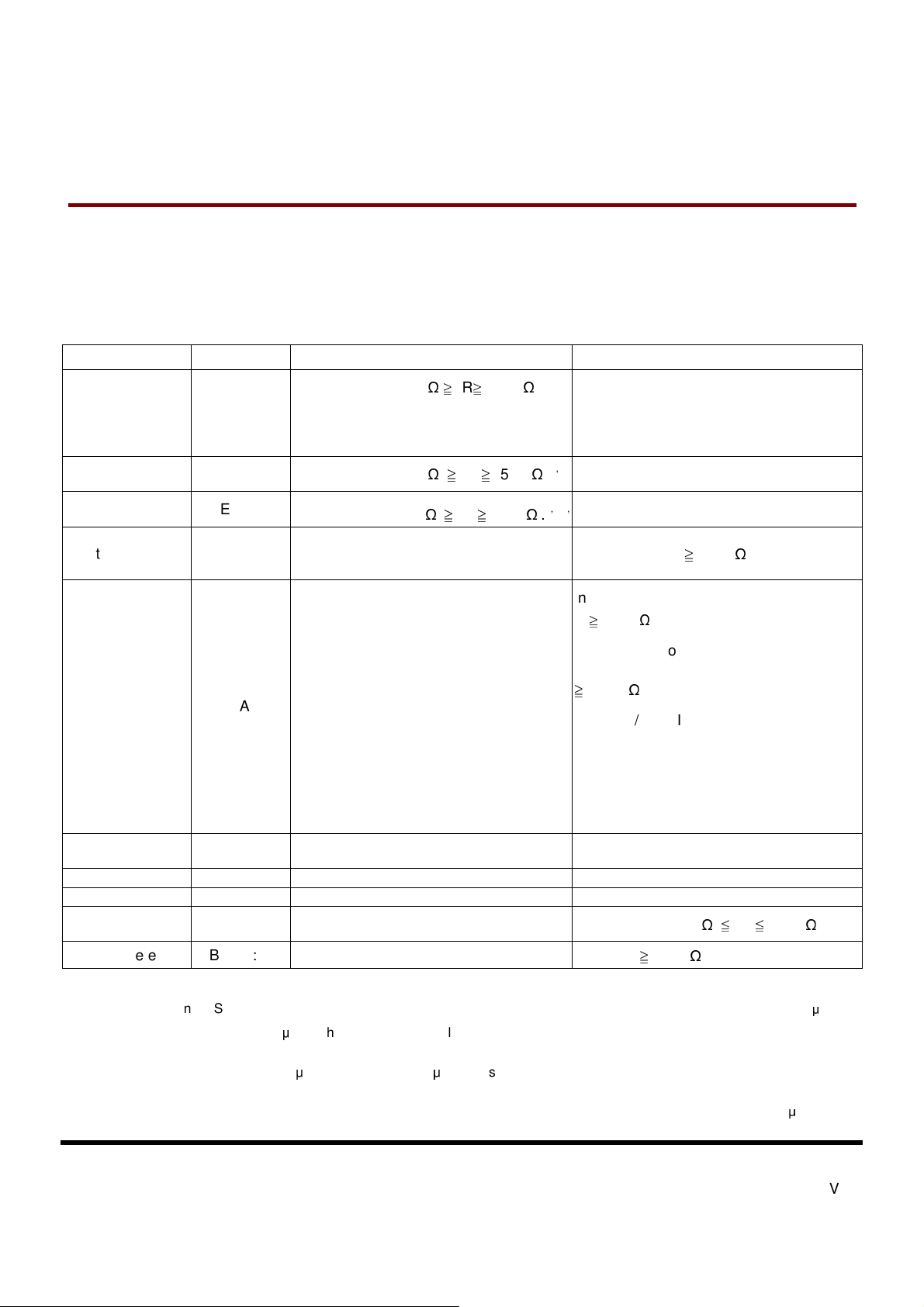
Pull-up to VCC 500 KΩ ≧ R ≧ 50 KΩ.
Pull-up to VCC 500 KΩ ≧ R ≧ 50 KΩ.
Ω ≧ R≧
50 KΩ and
1,2
1,2,9,
Pull-up to VCC R ≧ 10 KΩ.
In PCMCIA PC Card modes Pull-up to VCC
R ≧ 10 KΩ.4
In True IDE mode, if DMA operation is
supported by the host, Pull-down to Gnd R
≧
5.6 KΩ.5
PC Card / True IDE hosts switch the pullto pull down in True IDE mode if DMA
operation is supported.
The PC Card mode Pull-up may be left
active during True IDE mode if True IDE
DMA operation is not supported.
10
3
Address
Data Bus D[15:00]
Card Detect
Voltage Sense
Battery/Detect BVD[2:1]
A[10:00]
-CSEL
-CD[2:1] Connected to GND in the card
-VS1
-VS2
Notes: 1) Control Signals: each card shall present a load to the socket no larger than 50 pF
low state and 150 μA high state, including pull-resistor. The socket shall be able to drive at least the following
load
10
while meeting all AC timing requirements: (the number of sockets wired in parallel) multiplied by (50 pF
with DC current 700 μA low state and 150 μA high state per socket).
2) Resistor is optional.
3) Status Signals: the socket shall present a load to the card no larger than 50 pF
Transcend Information Inc.
1.
Pull-up to Vcc 10 KΩ ≦ R ≦100KΩ.
Pull-up R ≧ 50 KΩ.
10
10
at a DC current of 400 μA low
3.6
at a DC current of 700 μA
V1.0
Page 19

T
19
S
1
6
G
~
6
4
G
C
F
4
0
0
T
S
1
6
G
~
6
4
G
C
T
S
1
6
G
~
6
4
state and 100 μA high state, including pull-up resistor. The card shall be able to drive at least the following load
10
4) Status Signals: the socket shall present a load to the card no larger than 50 pF
state and 100 μA high state, including pull-up resistor. The card shall be able to drive at least the following load
10
5) Status Signals: the socket shall present a load to the card no larger than 50 pF
state and 100 μA high state, including pull-up resistor. The card shall be able to drive at least the following load
10
6) BVD2 was not defined in the JEIDA 3.0 release. Systems fully supporting JEIDA release 3 SRAM cards shall
pull-up pin 45 (BVD2) to avoid sensing their batteries as “Low.”
7) Address Signals: each card shall present a load of no more than 100pF
150μA high state. The host shall be able to drive at least the following load
requirements: (the number of sockets wired in parallel) multiplied by (100pF with DC current 450μA low state
and 150μA high state per socket).
8) Data Signals: the host and each card shall present a load no larger than 50pF
150μA high state. The host and each card shall be able to drive at least the following load
AC timing requirements: 100pF with DC current 1.6mA low state and 300μA high state. This permits the host to
wire two sockets in parallel without derating the card access speeds.
9) Reset Signal: This signal is pulled up to prevent the input from floating when a CFA to PCMCIA adapter is used
in a PCMCIA revision 1 host. However, to minimize DC current drain through the pull-up resistor in normal
operation the pull-up should be turned off once the Reset signal has been actively driven low by the host.
Consequently, the input is specified as an I2Z because the resistor is not necessarily detectable in the input
current leakage test.
10) Host and card restrictions for CF Advanced Timing Modes and Ultra DMA modes: Additional Requirements for
CF Advanced Timing Modes and Ultra DMA Electrical Requirements for additional required limitations on the
implementation of CF Advanced Timing modes and Ultra DMA modes respectively.
Additional Requirements for CF Advanced Timing Modes
The CF Advanced Timing modes include PC Card I/O and Memory modes that are 100ns or faster, PC Card Ultra
DMA modes 3 or above and True IDE PIO Modes 5,6, Multiword DMA Modes 3,4 and True IDE Ultra DMA modes
3 or above.
When operating in CF Advanced timing modes, the host shall conform to the following requirements:
1) Only one CF device shall be attached to the CF Bus.
2) The host shall not present a load of more than 40pF to the device for all signals, including any cabling.
3) The maximum cable length is 0.15 m (6 in). The cable length is measured from the card connector to the host
controller. 0.46 m (18 in) cables are
F
G
C
F
while meeting all AC timing requirements: 50 pF at a DC current of 400 μA low state and 100 μA high state.
while meeting all AC timing requirements: 50 pF at a DC current of 400 μA low state and 100 μA high state.
while meeting all AC timing requirements: 50 pF at a DC current of 400 μA low state and 1100 μA high state.
4
4
0
0
0
0
10
not
supported.
400X CompactFlash Card
at a DC current of 400 μA low
10
10
at a DC current of 400 μA low
at a DC current of 450μA low state and
while meeting all AC timing
10
10
at a DC current of 450μA and
while meeting all
10
4) The -WAIT and IORDY signals shall be ignored by the host.
Devices supporting CF Advanced timing modes shall also support slower timing modes, to ensure operability with
systems that do not support CF Advanced timing modes
Transcend Information Inc.
V1.0
Page 20
T
20
S
1
6
G
~
6
4
G
C
F
4
0
0
T
S
1
6
G
~
6
4
G
C
T
S
1
6
G
~
6
4
Ultra DMA Electrical Requirements
Host and Card signal capacitance limits for Ultra DMA operation
The host interface signal capacitance at the host connector shall be a maximum of 25 pF for each signal as measured at
1 MHz.
The card interface signal capacitance at the card connector shall be a maximum of 20 pF for each signal as measured at
1 MHz.
Series termination required for Ultra DMA operation
Series termination resistors are required at both the host and the card for operation in any of the Ultra DMA modes. Table
describes typical values for series termination at the host and the device.
G
C
F
F
4
4
0
0
0
0
400X CompactFlash Card
Table: Typical Series Termination for Ultra DMA
Signal Host Termination Device Termination
-HIOE (-HDMARDY,HSTROBE) 22 ohm 82 ohm
-IOWR (STOP) 22 ohm 82 ohm
-CS0, -CS1 33 ohm 82 ohm
A00, A01, A02 33 ohm 82 ohm
-DMACK 22 ohm 82 ohm
D15 through D00 33 ohm 33 ohm
DMARQ 82 ohm 22 ohm
INTRQ 82 ohm 22 ohm
IORDY (-DDMARDY, DSTROBE) 82 ohm 22 ohm
-RESET 33 ohm 82 ohm
NOTE
−
Only those signals requiring termination are listed in this table. If a signal is not listed, series
termination is not required for operation in an Ultra DMA mode. Shows signals also requiring a pull-up or
pull-down resistor at the host. The actual termination values should be selected to compensate for transceiver
and trace impedance to match the characteristic cable impedance.
Transcend Information Inc.
V1.0
Page 21
T
21
T
T
S
S
S
1
1
1
6
6
6
G
G
G
~
~
~
6
6
6
4
4
4
G
G
G
C
C
C
F
F
F
4
4
4
0
0
0
0
0
0
400X CompactFlash Card
Table: Ultra DMA Termination with Pull-up or Pull down Example
Printed Circuit Board (PCB) Trace Requirements for Ultra DMA
On any PCB for a host or device supporting Ultra DMA:
The longest D[15:00] trace shall be no more than 0.5" longer than either STROBE trace as measured from the
IC pin to the connector.
The shortest D[15:00] trace shall be no more than 0.5" shorter than either STROBE trace as measured from
the IC pin to the connector.
Ultra DMA Mode Cabling Requirement
Operation in Ultra DMA mode requires a crosstalk suppressing cable. The cable shall have a grounded line
between each signal line.
For True IDE mode operation using a cable with IDE (ATA) type 40 pin connectors it is recommended that the
host sense the cable type using the method described in the ANSI INCITS 361-2002 AT Attachment - 6
standard, to prevent use of Ultra DMA with a 40 conductor cable.
Transcend Information Inc.
V1.0
Page 22
T
22
S
1
6
G
~
6
4
G
C
F
4
0
0
T
S
1
6
G
~
6
4
G
C
T
S
1
6
G
~
6
4
Attribute Memory Read Timing Specification
Attribute Memory access time is defined as 300 ns. Detailed timing specs are shown in Table below
Speed Version 300 ns
Item
Read Cycle Time tc(R) tAVAV 300
Address Access Time ta(A) tAVQV 300
Card Enable Access Time ta(CE)
Output Enable Access Time ta(OE)
Output Disable Time from CE tdis(CE)
Output Disable Time from OE tdis(OE)
Address Setup Time tsu (A)
Output Enable Time from CE ten(CE)
Output Enable Time from OE ten(OE)
Data Valid from Address Change
Note: All times are in nanoseconds. Dout signifies data provided by the CompactFlash Storage Card to the system. The -CE signal or
both the -OE signal and the -WE signal shall be de-asserted between consecutive cycle operations.
G
F
C
F
4
4
0
0
0
0
400X CompactFlash Card
Symbol
tv(A) tAXQX 0
IEEE Symbol
tELQV 300
tGLQV 150
tEHQZ 100
tGHQZ 100
tAVGL 30
tELQNZ 5
tGLQNZ 5
Min ns.
Max ns.
Transcend Information Inc.
V1.0
Page 23
T
23
S
1
6
G
~
6
4
G
C
F
4
0
0
T
S
1
6
G
~
6
4
G
C
T
S
1
6
G
~
6
4
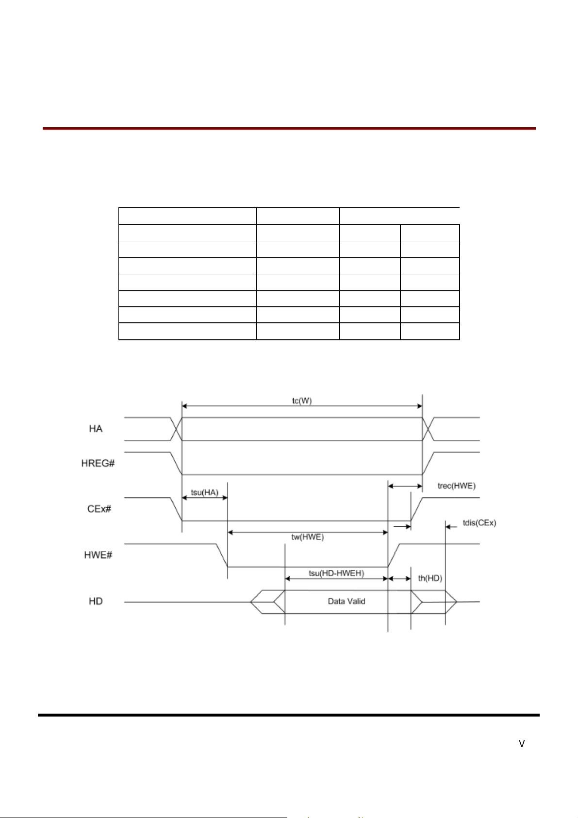
Configuration Register (Attribute Memory) Write Timing Specification
The Card Configuration write access time is defined as 250 ns. Detailed timing specifications are shown in Table
below.
G
C
F
F
4
0
0
4
0
0
Table: Configuration Register (Attribute Memory) Write Timing
400X CompactFlash Card
Speed Version
Item Symbol Min ns Max ns
Write Cycle Time tc(W) 250
Write Pulse Width tw(HWE) 150
Address Setup Time tsu(HA) 30
Write Recovery Time trec(HWE) 30
Data Setup Time for WE tsu(HD-HWEH) 80
Data Hold Time th(HD) 30
Note: All times are in nanoseconds. Din signifies data provided by the system to the CompactFlash Storage Card .
250 ns
Transcend Information Inc.
V1.0
Page 24
T
24
S
1
6
G
~
6
4
G
C
F
4
0
0
T
S
1
6
G
~
6
4
G
C
T
S
1
6
G
~
6
4
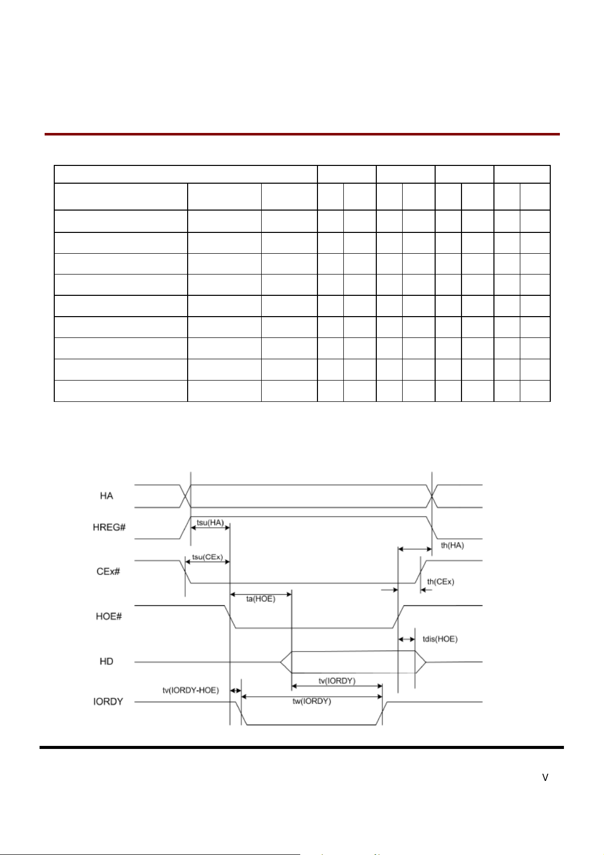
Common Memory Read Timing Specification
Item Symbol
G
C
F
F
4
4
0
0
0
0
Cycle Time Mode:
IEEE
Symbol
400X CompactFlash Card
250 ns 120 ns 100 ns 80 ns
Min
Max
Min
ns.
ns.
Max
ns.
ns.
Min
ns.
Max
ns.
Min
ns.
Max
ns.
Output Enable Access Time ta(HOE) tGLQV
Output Disable Time from HOE tdis(HOE) tGHQZ
Address Setup Time tsu(HA) tAVGL 30
Address Hold Time th(HA) tGHAX 20
CEx Setup before HOE tsu(CEx) tELGL 5
CEx Hold following HOE th(CEx) tGHEH 20
Wait Delay Falling from HOE tv(IORDY-HOE) tGLWTV
Data Setup for Wait Release tv(IORDY) tQVWTH
Wait Width Time
Notes:1) –WAIT is not supported in this mode.
2) The maximum load on -WAIT is 1 LSTTL with 50 pF (40pF below 120nsec Cycle Time) total load. All times are in
nanoseconds. Dout signifies data provided by the CompactFlash Storage Card to the system. The -WAIT signal may be
ignored if the -OE cycle to cycle time is greater than the Wait Width time. The Max Wait Width time can be determined from the
Card Information Structure. The Wait Width time meets the PCMCIA PC Card specification of 12µs but is intentionally less in
this specification.
2
tw(IORDY) tWTLWTH
125
100
35
0
350
15
15
5
15
60
60
35
0
350
10
15
5
15
50
50
10
10
10
35
0
350
45
45
5
1
na
na
na
1
1
Transcend Information Inc.
V1.0
Page 25
T
25
S
1
6
G
~
6
4
G
C
F
4
0
0
4
4
0
0
0
0
T
T
S
S
1
1
6
6
G
G
~
~
6
6
4
4
G
G
C
C
F
F
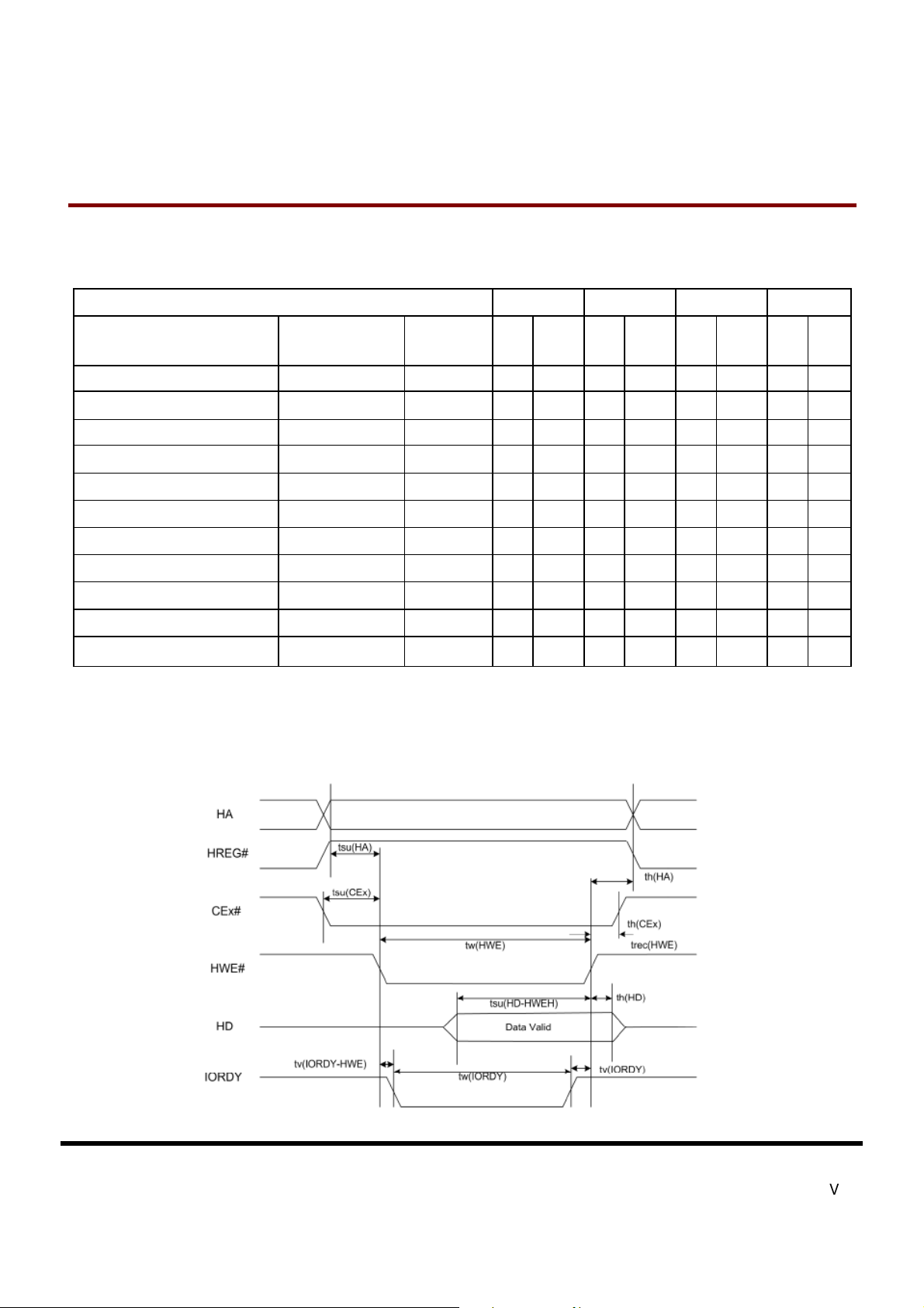
Common Memory Write Timing Specification
Cycle Time Mode: 250 ns 120 ns 100 ns 80 ns
Item Symbol
Data Setup before HWE tsu (HD-HWEH) tDVWH 80
Data Hold following HWE th(HD) tWMDX 30
HWE Pulse Width tw(HWE) tWLWH 150
Address Setup Time tsu(HA) tAVWL 30
CEx Setup before HWE tsu(CEx) tELWL 5
Write Recovery Time trec(HWE) tWMAX 30
Address Hold Time th(HA) tGHAX 20
CEx Hold following HWE th(CEx) tGHEH 20
Wait Delay Falling from HWE tv (IORDY-HWE) tWLWTV
WE High from Wait Release tv(IORDY) tWTHWH 0
Wait Width Time
2
tw (IORDY) tWTLWTH
IEEE
Symbol
Min
ns.
Max
ns.
35
350
400X CompactFlash Card
Min
ns.
50
15
70
15
5
15
15
15
0
Max
350
ns.
35
Min
Max
ns.
ns.
40
10
60
10
5
15
15
15
0
35
350
Min
ns.
30
10
55
10
5
15
15
10
na
Ma
x
ns.
1
na
1
1
na
Notes: 1) –WAIT is not supported in this mode.
2) The maximum load on -WAIT is 1 LSTTL with 50 pF (40pF below 120nsec Cycle Time) total load. All times are in
nanoseconds. Din signifies data provided by the system to the CompactFlash Storage Card. The -WAIT signal may be
ignored if the -HWE cycle to cycle time is greater than the Wait Width time. The Max Wait Width time can be determined
from the Card Information Structure. The Wait Width time meets the PCMCIA PC Card specification of 12µs but is
intentionally less in this specification.
Transcend Information Inc.
V1.0
Page 26
T
26
S
1
6
G
~
6
4
G
C
F
4
0
0
T
S
1
6
G
~
6
4
G
C
T
S
1
6
G
~
6
4
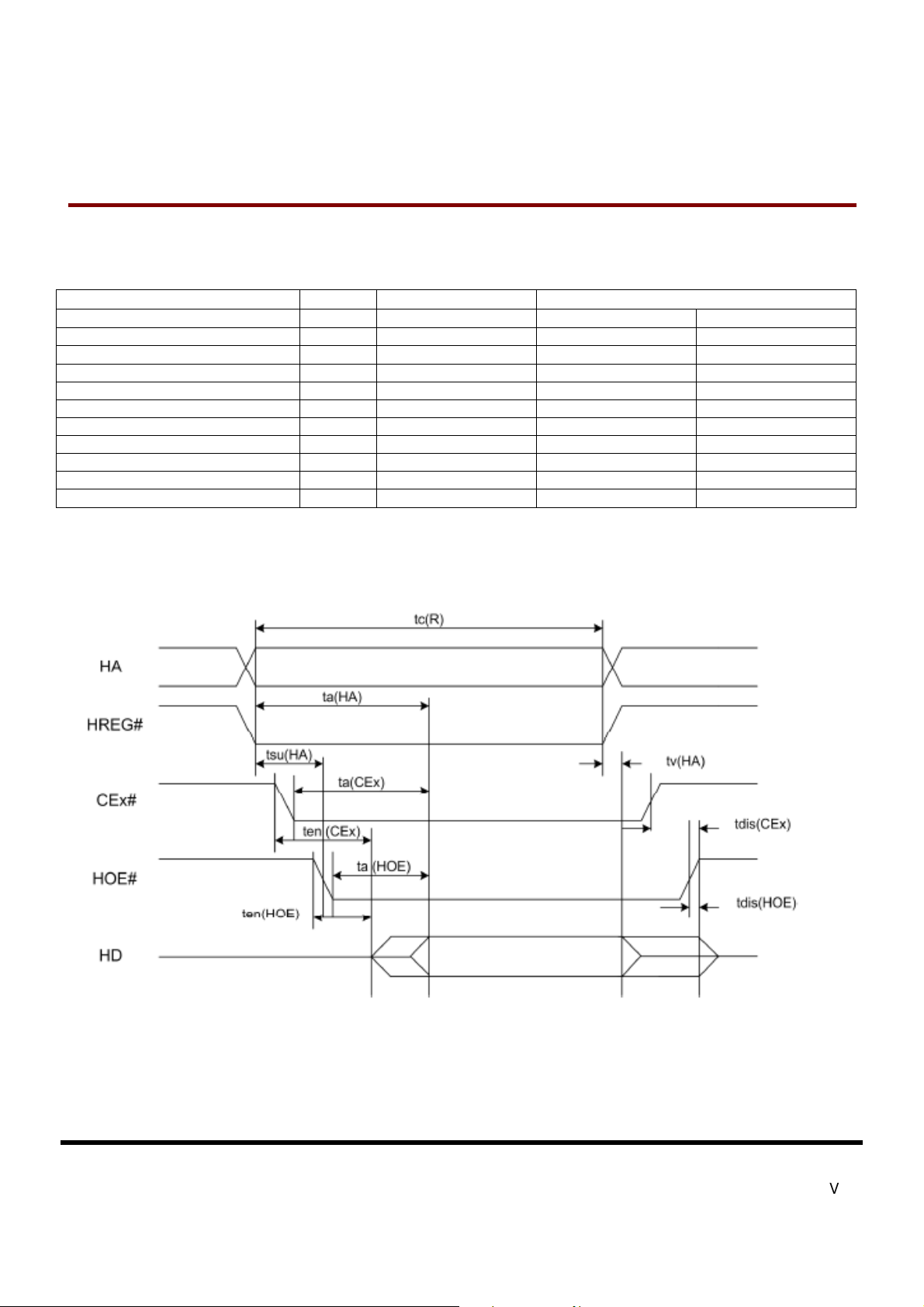
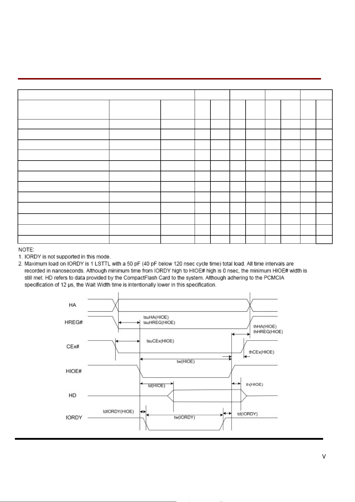
I/O Input (Read) Timing Specification
Data Delay after HIOE td(HIOE) tlGLQV
Data Hold following HIOE th(HIOE) tlGHQX 0
HIOE Width Time tw(HIOE) tlGLIGH 165
Address Setup before HIOE tsuA(HIOE) tAVIGL 70
Address Hold following HIOE thA(HIOE) tlGHAX 20
CEx Setup before HIOE tsuCE(HIOE) tELIGL 5
CEx Hold following HIOE thCE(HIOE) tlGHEH 20
HREG Setup before HIOE tsuREG (HIOE) tRGLIGL 5
F
G
C
F
Item Symbol
4
4
0
0
0
0
Cycle Time Mode: 250 ns 120 ns 100 ns 80 ns
IEEE
Symbol
Min
ns.
Max
ns.
100
400X CompactFlash Card
Min
ns.
5
70
25
10
5
10
5
Max
50
ns.
Min
ns.
5
65
25
10
5
10
5
Max
ns.
50
Min
ns.
5
55
15
10
5
10
5
Ma
x
ns.
45
HREG Hold following HIOE thREG (HIOE) tlGHRGH 0
Wait Delay Falling from HIOE2 tdWT(HIOE) tlGLWTL
Data Delay from Wait Rising2 td(IORDY) tWTHQV
Wait Width Time2 tw(IORDY) tWTLWTH
0
35
0
350
35 35 Na
350
0
0 0 Na
350
0
Na
1
1
1
Transcend Information Inc.
V1.0
Page 27
T
27
S
1
6
G
~
6
4
G
C
F
4
0
0
T
S
1
6
G
~
6
4
G
C
T
S
1
6
G
~
6
4
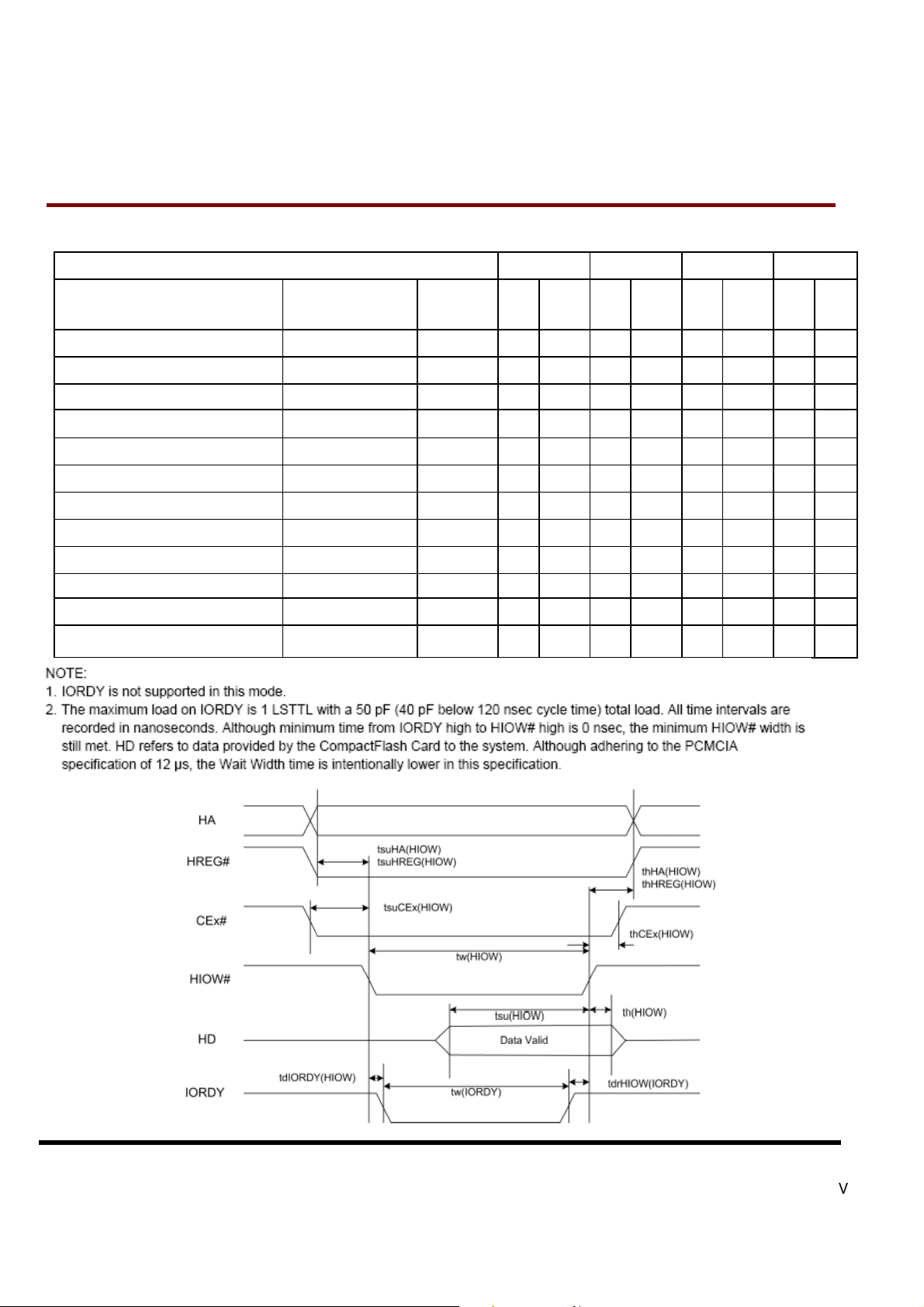
I/O Output (Write) Timing Specification
Data Setup before HIOW tsu(HIOW) tDVIWH 60
G
Item
C
F
F
4
4
0
0
0
0
Cycle Time Mode: 255 ns 120 ns 100 ns 80 ns
Symbol
IEEE
Symbol
Min
ns.
400X CompactFlash Card
Max
Min
Max
ns.
ns.
ns.
20 20 15
Min
ns.
Max
ns.
Min
ns.
Ma
x
ns.
Data Hold following HIOW th(HIOW) tlWHDX 30
HIOW Width Time tw(HIOW) tlWLIWH 165 70 65 55
Address Setup before HIOW tsuA(HIOW) tAVIWL 70
Address Hold following HIOW thA(HIOW) tlWHAX 20
CEx Setup before HIOW tsuCE (HIOW) tELIWL 5
CEx Hold following HIOW thCE (HIOW) tlWHEH 20
HREG Setup before HIOW tsuREG (HIOW) tRGLIWL 5
HREG Hold following HIOW thREG (HIOW) tlWHRGH 0
Wait Delay Falling from HIOW2 tdWT(HIOW) tlWLWTL
HIOW high from Wait high2 tdrHIOW (IORDY) tWTJIWH 0
Wait Width Time2 tw(IORDY)
tWTLWT
H
10 5 5
25 25 15
20 10 10
5 5 5
20 10 10
5 5 5
0 0 0
35
350 350
35 35 Na1
0 0 Na1
350
Na1
Transcend Information Inc.
V1.0
Page 28

T
28
S
1
6
G
~
6
4
G
C
F
4
0
0
T
S
1
6
G
~
6
4
G
C
T
S
1
6
G
~
6
4
True IDE PIO Mode Read/Write Timing Specification
t0 Cycle time (min) 600 383 240 180 120 100 80 1
t1
t2 HIOE/HIOW (min) 165 125 100 80 70 65 55 1
t2 HIOE/HIOW (min) Register (8 bit) 290 290 290 80 70 65 55 1
t2i HIOE/HIOW recovery time (min) - - - 70 25 25 20 1
t3 HIOW data setup (min) 60 45 30 30 20 20 15
F
G
C
F
Item
Address Valid to HIOE/HIOW
setup (min)
4
4
0
0
0
0
400X CompactFlash Card
Mode
0 1 2 3 4 5 6
70 50 30 30 25 15 10
Note
t4 HIOW data hold (min) 30 20 15 10 10 5 5
t5 HIOE data setup (min) 50 35 20 20 20 15 10
t6 HIOE data hold (min) 5 5 5 5 5 5 5
T6Z HIOE data tristate (max) 30 30 30 30 30 20 20 2
Address valid to -IOCS16
t7
assertion (max)
Address valid to -IOCS16 released
t8
(max)
t9 HIOE/HIOW to address valid hold 20 15 10 10 10 10 10
Read Data Valid to IORDY active
tRD
(min), if IORDY initially low after tA
tA IORDY Setup time 35 35 35 35 35 na
tB IORDY Pulse Width (max) 1250 1250 1250 1250 1250 na
tC IORDY assertion to release (max) 5 5 5 5 5 na
Notes: All timings are in nanoseconds. The maximum load on -IOCS16 is 1 LSTTL with a 50 pF (40pF below 120nsec Cycle Time) total load.
All times are in nanoseconds. Minimum time from -IORDY high to -HIOE high is 0 nsec, but minimum -HIOE width shall still be met.
1) t0 is the minimum total cycle time, t2 is the minimum command active time, and t2i is the minimum command recovery time or
command inactive time. The actual cycle time equals the sum of the actual command active time and the actual command inactive
time. The three timing requirements of t0, t2, and t2i shall be met. The minimum total cycle time requirement is greater than the
sum of t2 and t2i. This means a host implementation can lengthen either or both t2 or t2i to ensure that t0 is equal to or greater than
the value reported in the device’s identify device data. A CompactFlash Storage Card implementation shall support any legal host
implementation.
2) This parameter specifies the time from the negation edge of -HIOE to the time that the data bus is no longer driven by the
CompactFlash Storage Card (tri-state).
3) The delay from the activation of -HIOE or -HIOW until the state of IORDY is first sampled. If IORDY is inactive then the host shall
wait until IORDY is active before the PIO cycle can be completed. If the CompactFlash Storage Card is not driving IORDY negated
at tA after the activation of -HIOE or -HIOW, then t5 shall be met and tRD is not applicable. If the CompactFlash Storage Card is
driving IORDY negated at the time tA after the activation of -HIOE or -HIOW, then tRD shall be met and t5 is not applicable.
4) t7 and t8 apply only to modes 0, 1 and 2. For other modes, this signal is not valid.
5) IORDY is not supported in this mode.
90 50 40 n/a n/a n/a n/a 4
60 45 30 n/a n/a n/a n/a 4
0 0 0 0 0 0 0
5
na5 3
5
na5
5
na
5
Transcend Information Inc.
V1.0
Page 29

T
29
T
T
S
S
S
1
1
1
6
6
6
G
G
G
~
~
~
6
6
6
4
4
4
G
G
G
C
C
C
F
F
F
4
4
4
0
0
0
0
0
0
400X CompactFlash Card
Transcend Information Inc.
V1.0
Page 30

T
30
S
1
6
G
~
6
4
G
C
F
4
0
0
4
4
0
0
0
0
T
T
S
S
1
1
6
6
G
G
~
~
6
6
4
4
G
G
C
C
F
F
True IDE Multiword DMA Mode Read/Write Timing Specification
t
Cycle time (min) 480 150 120 100 80 1
O
t
-HIOE / -HIOW asserted width (min) 215 80 70 65 55 1
D
t
-HIOE data access (max) 150 60 50 50 45
E
t
-HIOE data hold (min) 5 5 5 5 5
F
t
G
-HIOE/-HIOW data setup (min) 100 30 20 15 10
t
H
-HIOW data hold (min) 20 15 10 5 5
t
I
-HREG to –HIOE/-HIOW setup (min) 0 0 0 0 0
t
-HIOE / -HIOW to -HREG hold (min) 20 5 5 5 5
J
t
-HIOE negated width (min) 50 50 25 25 20 1
KR
t
KW
-HIOW negated width (min) 215 50 25 25 20 1
t
LR
-HIOE to DMARQ delay (max) 120 40 35 35 35
t
LW
-HIOW to DMARQ delay (max) 40 40 35 35 35
t
M
CEx valid to –HIOE / -HIOW 50 30 25 10 5
t
N
CEx hold 15 10 10 10 10
Item
Mode 0
(ns)
Mode 1
(ns)
Mode 2
(ns)
400X CompactFlash Card
Mode 3
(ns)
Mode 4
(ns)
Note
Transcend Information Inc.
V1.0
Page 31

T
31
T
T
S
S
S
1
1
1
6
6
6
G
G
G
~
~
~
6
6
6
4
4
4
G
G
G
C
C
C
F
F
F
4
4
4
0
0
0
0
0
0
400X CompactFlash Card
True IDE Ultra DMA Mode Read/Write Timing Specification
Ultra DMA operations can take place in any of the three basic interface modes: PC Card Memory mode, PC Card I/O mode,
Transcend Information Inc.
V1.0
Page 32

T
32
S
1
6
G
~
6
4
G
C
F
4
0
0
T
S
1
6
G
~
6
4
G
C
T
S
1
6
G
~
6
4
and True IDE (the original mode to support UDMA). The usage of signals in each of the modes is shown in Table 24:Ultra DMA
Signal Usage In Each Interface Mode
UDMA Signal Type
DMARQ Output 43 (-INPACK) -DMARQ -DMARQ DMARQ
G
C
F
F
4
4
0
0
0
0
Pin # (Non
UDMA MEM
MODE)
PC CARD MEM
MODE UDMA
400X CompactFlash Card
PC CARD IO MODE
UDMA
TRUE IDE MODE
UDMA
HREG Input
HIOW Input
HIOE Input
IORDY Output
HD [15:0] Bidir
HA [10:0] Input
CSEL Input
HIRQ Output 37 (READY) READY -INTRQ INTRQ
CE1
CE2
Notes:1) The UDMA interpretation of this signal is valid only during an Ultra DMA data burst.
2) The UDMA interpretation of this signal is valid only during and Ultra DMA data burst during a DMA Read command.
3) The UDMA interpretation of this signal is valid only during an Ultra DMA data burst during a DMA Write command.
4) The HSTROBE and DSTROBE signals are active on both the rising and the falling edge.
5) Address lines 03 through 10 are not used in True IDE mode.
Several signal lines are redefined to provide different functions during an Ultra DMA data burst. These lines assume their
UDMA definitions when:
1 an Ultra DMA mode is selected, and
2 a host issues a READ DMA, or a WRITE DMA command requiring data transfer, and
3 the device asserts (-)DMARQ, and
4 the host asserts (-)DMACK.
These signal lines revert back to the definitions used for non-Ultra DMA transfers upon the negation of -DMACK by the host at
the termination of an Ultra DMA data burst.
Input
44 (-REG) -DMACK DMACK -DMACK
35 (-HIOW) STOP 1 STOP 1 STOP 1
34 (-HIOE)
42 (-WAIT)
… (D[15:00]) D[15:00] D[15:00] D[15:00]
… (A[10:00]) A[10:00] A[10:00] A[02:00] 5
39 (-CSEL) -CSEL -CSEL -CSEL
7 (-CE1)
31 (-CE2)
-HDMARDY(R) 1,
2HSTROBE(W)
-DDMARDY(W)
DSTROBE(R)
-CE1
-CE2
1. 2. 4
1, 3, 4
1, 3
-HDMARDY(R)
HSTROBE(W)
-DDMARDY(W)
DSTROBE(R)
-CE1
-CE2
1, 2
1, 3, 4
1, 3
1. 2. 4
-HDMARDY(R)
HSTROBE(W)
-DDMARDY(W)
DSTROBE(R)
-CS0
-CS1
1, 2
1, 3, 4
1, 3
1. 2. 4
With the Ultra DMA protocol, the STROBE signal that latches data from D[15:00] is generated by the same agent (either host
or device) that drives the data onto the bus. Ownership of D[15:00] and this data strobe signal are given either to the device
during an Ultra DMA data-in burst or to the host for an Ultra DMA data-out burst.
During an Ultra DMA data burst a sender shall always drive data onto the bus, and, after a sufficient time to allow for
propagation delay, cable settling, and setup time, the sender shall generate a STROBE edge to latch the data. Both edges of
STROBE are used for data transfers so that the frequency of STROBE is limited to the same frequency as the data.
Words in the IDENTIFY DEVICE data indicate support of the Ultra DMA feature and the Ultra DMA modes the device is
capable of supporting. The Set transfer mode subcommand in the SET FEATURES command shall be used by a host to
select the Ultra DMA mode at which the system operates. The Ultra DMA mode selected by a host shall be less than or equal
to the fastest mode of which the device is capable. Only one Ultra DMA mode shall be selected at any given time. All timing
requirements for a selected Ultra DMA mode shall be satisfied. Devices supporting any Ultra DMA mode shall also support all
slower Ultra DMA modes.
Transcend Information Inc.
V1.0
Page 33

T
33
S
1
6
G
~
6
4
G
C
F
4
0
0
T
S
1
6
G
~
6
4
G
C
T
S
1
6
G
~
6
4
An Ultra DMA capable device shall retain the previously selected Ultra DMA mode after executing a software reset sequence
or the sequence caused by receipt of a DEVICE RESET command if a SET FEATURES disable reverting to defaults
command has been issued. The device may revert to a Multiword DMA mode if a SET FEATURES enable reverting to default
has been issued. An Ultra DMA capable device shall clear any previously selected Ultra DMA mode and revert to the default
non-Ultra DMA modes after executing a power-on or hardware reset.
Both the host and device perform a CRC function during an Ultra DMA data burst. At the end of an Ultra DMA data burst the
host sends its CRC data to the device. The device compares its CRC data to the data sent from the host. If the two values do
not match, the device reports an error in the error register. If an error occurs during one or more Ultra DMA data bursts for any
one command, the device shall report the first error that occurred. If the device detects that a CRC error has occurred before
data transfer for the command is complete, the device may complete the transfer and report the error or abort the command
and report the error.
NOTE -If a data transfer is terminated before completion, the assertion of INTRQ should be passed through to the host
software driver regardless of whether all data requested by the command has been transferred.
G
C
F
F
4
4
0
0
0
0
400X CompactFlash Card
Transcend Information Inc.
V1.0
Page 34

T
34
T
T
S
S
S
1
1
1
6
G
6
G
6
Name
t
t
t
t
t
t
t
t
t
t
t
t
t
t
t
~
6
~
6
G
~
2CYCTYP
CYC
2CYC
DS
DH
DVS
DVH
CS
CH
CVS
CVH
ZFS
DZFS
FS
LI
4
G
C
F
4
0
0
4
G
C
6
4
F
G
C
F
UDMA Mode
0
Min Max Min Max Min Max Min Max Min Max Min Max Min Max
240
112
230
15.0
5.0
70.0
6.2
15.0
5.0
70.0
6.2
0
70.0
0 150 0 150 0 150 0 100 0 100 0 75 0 60 Note 4
4
4
230
0
0
0
0
160
153
10.0
48.0
10.0
48.0
48.0
UDMA
Mode 1
73
5.0
6.2
5.0
6.2
0
200
UDMA
Mode 2
120
54
115
7.0
5.0
31.0
6.2
7.0
5.0
31.0
6.2
0
31.0
170
400X CompactFlash Card
UDMA
Mode 3
90
39
86
7.0
5.0
20.0
6.2
7.0
5.0
20.0
6.2
0
20.0
130
UDMA
Mode 4
60
25
57
5.0
5.0
6.7
6.2
5.0
5.0
6.7
6.2
0
6.7
120
UDMA
Mode 5
40
16.8
38
4.0
4.6
4.8
4.8
5.0
5.0
10.0
10.0
35
25
90 80 Device
UDMA
Mode 6
30 Sender
13.0 Note 3
29 Sender
2.6
3.5
4.0
4.0
5.0
5.0
10.0 Host
10.0 Host
25 Device
17.5 Sender
Measure
location (see
Note 2)
Recipient
Recipient
Sender
Sender
Device
Device
Notes:
t
MLI
t
UI
t
AZ
t
ZAH
t
ZAD
t
ENV
t
RFS
t
RP
t
IORDYZ
t
ZIORDY
t
ACK
t
SS
20
0
20
0
20 70 20 70 20 70 20 55 20 55 20 50 20 50 Host
160
0
20
50
1) All timing measurement switching points (low to high and high to low) shall be taken at 1.5 V.
2) All signal transitions for a timing parameter shall be measured at the connector specified in the measurement location
column. For example, in the case of tRFS, both STROBE and –DMARDY transitions are measured at the sender
connector.
3) The parameter tCYC shall be measured at the recipient’s connector farthest from the sender.
10
75
20
20
0
20
0
125
0
20
50
10
70
20
20
0
20
0
100
0
20
50
10
60
20
20
0
20
0
100
0
20
50
10
60
20
20
0
20
0
100
0
20
50
10
60
20
20
0
20
0
85
0
20
50
20 Host
0 Host
10 10 Note 5
20 Host
0 Device
50 50 Sender
85 Recipient
20 20 Device
0 Device
20 Host
50 Sender
Transcend Information Inc.
V1.0
Page 35

T
35
T
T
S
S
S
1
1
1
6
G
~
6
4
G
C
F
4
0
0
6
G
~
6
4
G
C
6
G
~
6
4
4) The parameter tLI shall be measured at the connector of the sender or recipient that is responding to an incoming
transition from the recipient or sender respectively. Both the incoming signal and the outgoing response shall be
measured at the same connector.
5) The parameter tAZ shall be measured at the connector of the sender or recipient that is driving the bus but must release the
bus the allow for a bus turnaround.
Name Comment
G
C
F
F
4
4
0
0
0
0
400X CompactFlash Card
Notes
t
2CYCTYP
t
CYC
t
2CYC
t
DS
t
DH
t
DVS
t
DVH
t
CS
t
CH
t
CVS
t
CVH
t
ZFS
t
DZFS
t
FS
t
LI
t
MLI
t
UI
t
AZ
t
ZAH
t
ZAD
t
ENV
t
RFS
t
RP
t
IORDYZ
t
ZIORDY
t
ACK
t
SS
Typical sustained average two cycle time
Cycle time allowing for asymmetry and clock variations (from STROBE edge to STROBE edge)
Two cycle time allowing for clock variations (from rising edge to next rising edge or from falling edge to
next falling edge of STROBE)
Data setup time at recipient (from data valid until STROBE edge) 2, 5
Data hold time at recipient (from STROBE edge until data may become invalid) 2, 5
Data valid setup time at sender (from data valid until STROBE edge) 3
Data valid hold time at sender (from STROBE edge until data may become invalid) 3
CRC word setup time at device 2
CRC word hold time device 2
CRC word valid setup time at host (from CRC valid until -DMACK negation) 3
CRC word valid hold time at sender (from -DMACK negation until CRC may become invalid) 3
Time from STROBE output released-to-driving until the first transition of critical timing.
Time from data output released-to-driving until the first transition of critical timing.
First STROBE time (for device to first negate DSTROBE from STOP during a data in burst)
Limited interlock time 1
Interlock time with minimum 1
Unlimited interlock time 1
Maximum time allowed for output drivers to release (from asserted or negated)
Minimum delay time required for output
drivers to assert or negate (from released)
Envelope time (from -DMACK to STOP and -HDMARDY during data in burst initiation and from DMACK
to STOP during data out burst initiation)
Ready-to-final-STROBE time (no STROBE edges shall be sent this long after negation of -DMARDY)
Ready-to-pause time (that recipient shall wait to pause after negating -DMARDY)
Maximum time before releasing IORDY 6
Minimum time before driving IORDY 4, 6
Setup and hold times for -DMACK (before assertion or negation)
Time from STROBE edge to negation of DMARQ or assertion of STOP (when sender terminates a
burst)
Transcend Information Inc.
V1.0
Page 36

T
36
S
1
6
G
~
6
4
G
C
F
4
0
0
T
S
1
6
G
~
6
4
G
C
T
S
1
6
G
~
6
4
Notes: 1) The parameters tUI, tMLI : (Ultra DMA Data-In Burst Device Termination Timing and Ultra DMA Data-In
Burst Host Termination Timing), and tLI indicate sender-to-recipient or recipient-to-sender interlocks, i.e.,
one agent (either sender or recipient) is waiting for the other agent to respond with a signal before
proceeding. tUI is an unlimited interlock that has no maximum time value. tMLI is a limited time-out that
has a defined minimum. tLI is a limited time-out that has a defined maximum.
2) 80-conductor cabling shall be required in order to meet setup (tDS, tCS) and hold (tDH, tCH) times in
modes greater than 2.
3) Timing for tDVS, tDVH, tCVS and tCVH shall be met for lumped capacitive loads of 15 and 40 pF at the
connector where the Data and STROBE signals have the same capacitive load value. Due to reflections
on the cable, these timing measurements are not valid in a normally functioning system.
4)For all modes the parameter tZIORDY may be greater than tENV due to the fact that the host has a
pull-up on IORDY- giving it a known state when released.
5)The parameters tDS, and tDH for mode 5 are defined for a recipient at the end of the cable only in a
configuration with a single device located at the end of the cable. This could result in the minimum values
for tDS and tDH for mode 5 at the middle connector being 3.0 and 3.9 ns respectively.
G
C
F
F
4
4
0
0
0
0
400X CompactFlash Card
UDMA
Name
t
DSIC
t
DHIC
t
DVSIC
t
DVHIC
t
DSIC
t
DHIC
t
DVSIC
t
DVHIC
Notes: 1) All timing measurement switching points(low to high and high to low) shall be taken at 1.5 V.
Mode 0
(ns)
Min Max Min Max Min Max Min Max Min Max Min Max Min Max
14.7
4.8
72.9
9.0
Recipient IC data setup time (from data valid until STROBE edge) (see note 2)
Recipient IC data hold time (from STROBE edge until data may become invalid) (see note 2)
Sender IC data valid setup time (from data valid until STROBE edge) (see note 3)
Sender IC data valid hold time (from STROBE edge until data may become invalid) (see note 3)
2) The correct data value shall be captured by the recipient given input data with a slew rate of 0.4 V/ns
rising and falling and the input STROBE with a slew rate of 0.4 V/ns rising and falling at tDSIC and tDHIC
timing (as measured through 1.5 V).
3)The parameters tDVSIC and tDVHIC shall be met for lumped capacitive loads of 15 and 40 pF at the IC
where all signals have the same capacitive load value. Noise that may couple onto the output signals from
external sources has not been included in these values.
UDMA
Mode 1
(ns)
9.7
4.8
50.9
9.0
UDMA
Mode 2
6.8
4.8
33.9
9.0
(ns)
UDMA
Mode 3
(ns)
6.8
4.8
22.6
9.0
UDMA
Mode4
4.8
4.8
9.5
9.0
(ns)
UDMA
Mode 5
2.3
2.8
6.0
6.0
(ns)
UDMA
Mode 6
(ns)
2.3
2.8
5.2
5.2
Transcend Information Inc.
V1.0
Page 37

T
37
T
T
S
S
S
1
1
1
6
6
6
G
G
G
~
~
~
6
6
6
4
4
4
G
G
G
C
C
C
F
F
F
4
4
4
0
0
0
0
0
0
400X CompactFlash Card
Name
S
RISE
S
FALL
Note: 1) The sender shall be tested while driving an 18 inch long, 80 conductor cable with PVC insulation material.
The signal under test shall be cut at a test point so that it has not trace, cable or recipient loading after the
test point. All other signals should remain connected through to the recipient. The test point may be located
at any point between the sender’s series termination resistor and one half inch or less of conductor exiting
the connector. If the test point is on a cable conductor rather than the PCB, an adjacent ground conductor
shall also be cut within one half inch of the connector.
The test load and test points should then be soldered directly to the exposed source side connectors. The
test loads consist of a 15 pF or a 40 pF, 5%, 0.08 inch by 0.05 inch surface mount or smaller size capacitor
from the test point to ground. Slew rates shall be met for both capacitor values.
Measurements shall be taken at the test point using a <1 pF, >100 Kohm, 1 Ghz or faster probe and a 500
MHz or faster oscilloscope. The average rate shall be measured from 20% to 80% of the settled VOH level
with data transitions at least 120 nsec apart. The settled VOH level shall be measured as the average
output high level under the defined testing conditions from 100 nsec after 80% of a rising edge until 20% of
the subsequent falling edge.
Comment Min
[V/ns]
Rising Edge Slew Rate for any signal
Falling Edge Slew Rate for any signal
Max
[V/ns]
1.25 1
1.25 1
Notes
Transcend Information Inc.
V1.0
Page 38

T
38
S
1
6
G
~
6
4
G
C
F
4
0
0
4
4
0
0
0
0
XX X X X X Standby and UDMA transfer
XX X X X 0 Configuration Registers Read
XX X X X X Common Memory Read (8 Bit D7-D0)
XX X X X X Common Memory Read (8 Bit D15-D8)
XX X X X 0 Common Memory Read (16 Bit D15-D0)
XX X X X 0 Configuration Registers Write
XX X X X X Common Memory Write (8 Bit D7-D0)
XX X X X X Common Memory Write (8 Bit D15-D8)
XX X X X 0 Common Memory Write (16 Bit D15-D0)
XX X X X 0 Card Information Structure Read
XX X X X 0 Invalid Access (CIS Write)
XX X X X 1 Invalid Access (Odd Attribute Read)
XX X X X 1 Invalid Access (Odd Attribute Write)
XX X X X X Invalid Access (Odd Attribute Read)
XX X X X X Invalid Access (Odd Attribute Write)
400X CompactFlash Card
SELECTED SPACE
T
S
1
6
G
~
6
4
G
C
T
S
1
6
G
~
6
4
Card Configuration
The CompactFlash Storage Cards is identified by appropriate information in the Card Information Structure (CIS). The
following configuration registers are used to coordinate the I/O spaces and the Interrupt level of cards that are located
in the system. In addition, these registers provide a method for accessing status information about the CompactFlash
Storage Card that may be used to arbitrate between multiple interrupt sources on the same interrupt level or to
replace status information that appears on dedicated pins in memory cards that have alternate use in I/O cards.
Multiple Function CompactFlash Storage Cards
-CE2 -CE1 -REG -OE -WE A10 A9 A8-A4 A3 A2 A1 A0
1 1 X X X X X
X 0 0 0 1 0 1
1 0 1 0 1 X X
0 1 1 0 1 X X
0 0 1 0 1 X X
X 0 0 1 0 0 1
1 0 1 1 0 X X
0 1 1 1 0 X X
0 0 1 1 0 X X
X 0 0 0 1 0 0
1 0 0 1 0 0 0
1 0 0 0 1 X X
1 0 0 1 0 X X
0 1 0 0 1 X X
0 1 0 1 0 X X
F
G
C
F
Table: CompactFlash Storage Card Registers and Memory Space Decoding
Transcend Information Inc.
V1.0
Page 39

T
39
0 1
0 1
0 1
0 1
0 1
0 1
0 1
0 1
S
1
6
G
~
6
4
G
C
F
4
0
0
4
4
0
0
0
0
400X CompactFlash Card
T
T
S
S
1
1
6
6
G
G
~
~
6
6
4
4
G
G
C
C
F
F
Table: PC Card Memory Mode UDMA Function
W
-DMARDY
-HIOE
(R)-WAIT
(W)
-CE2 -CE1
1 1 1 X X X X No XX Standby
X X
X X 0 1 1 X 1 YES XX Host Acknowledge Preparation
1 1 0 1 1 1 1 YES Static Host Acknowledge Preparation
1 1 0 0 1 1 1 YES Static DMA Acknowledge (Stopped)
1 1 0 0 0 0 1 YES Static Burst Initiation / Active
1 1 0 0 0 X / or \ YES Static Burst Transfer
1 1 0 0 0 1 0 or 1 RD Static Data In Burst Host Pause
1 1 0 0 0 0 0 or 1 RD Static Data In Burst Device Pause
1 1 0 0 0 1 0 or 1 WR Static Data Out Burst Device Pause
1 1 0 0 0 0 0 or 1 WR Static Data Out Burst Host Pause
1 1 1 0 0 0 0 or 1 RD Static Device Initiating BurstTermination
-DMARQ
-INPACK
0 1 X X 1 YES XX
-DMACK
-REG
STOP
-HIO
STROBE
-WAIT
(R)-HIOE
(W)
DMA
CMD
A10-
A00
Operation
Device UDMA Transfer Request
(Assert DMARQ)
1 1 1 0 1 1 0 or 1 RD Static
1 1 0 0 1 0 0 or 1 YES Static Host Initiating BurstTermination
1 1 1 0 1 1 0 or 1 YES Static
1 1 1 0 1 1 / YES Static
1 1 1 / 1 1 1 YES Static CRC Data Transfer for UDMA Burst
1 1 1 1 1 1 1 YES Static Burst Completed
Host Acknowledement of Device
Initiated Burst Termination
Device Acknowledging Host Initiated
Burst Termination
Device Aligning STROBE to Asserted
before CRC Transfer
Table: CompactFlash Storage Card Configuration Registers Decoding
-CE2 -CE1 -REG -OE -WE A10 A9 A8-A4 A3 A2 A1 A0 SELECTED REGISTER
X 0 0 0 1
X 0 0 1 0
X 0 0 0 1
X 0 0 1 0
X 0 0 0 1
X 0 0 1 0
X 0 0 0 1
X 0 0 1 0
00 0 0 0 0 Configuration Option Reg Read
00 0 0 0 0 Configuration Option Reg Write
00 0 0 1 0 Card Status Register Read
00 0 0 1 0 Card Status Register Write
00 0 1 0 0 Pin Replacement Register Read
00 0 1 0 0 Pin Replacement Register Write
00 0 1 1 0 Socket and Copy Register Read
00 0 1 1 0 Socket and Copy Register Write
Transcend Information Inc.
V1.0
Page 40

T
40
S
1
6
G
~
6
4
G
C
F
4
0
0
4
4
0
0
0
0
400X CompactFlash Card
T
T
S
S
1
1
6
6
G
G
~
~
6
6
4
4
G
G
C
C
F
F
Attribute Memory Function
Attribute memory is a space where CompactFlash Storage Card identification and configuration information are
stored, and is limited to 8 bit wide accesses only at even addresses. The card configuration registers are also
located here. For CompactFlash Storage Cards, the base address of the Card configuration registers is 200h.
Function Mode DMA CMD -REG -CE2 -CE1 A10 A9 A0 -OE -WE D15-D8 D7-D0
Table: Attribute Memory Function
Standby Mode Don’t Care
Standby Mode No X H H X X X X X High Z High Z
UDMA Operation (see section
4.3.18: Ultra DMA Mode
Read/Write Timing
Specification)
Read Byte Access CIS ROM
(8 bits)
Write Byte Access CIS (8 bits)
(Invalid)
Read Byte Access
Configuration CompactFlash
Storage (8 bits)
Write Byte Access
Configuration CompactFlash
Storage (8 bits)
Read Word Access CIS (16
bits)
Write Word Access CIS (16
bits) (Invalid)
Read Word Access
Configuration CompactFlash
Storage (16 bits)
Write Word Access
Configuration CompactFlash
Storage (16 bits)
Notes: 1) In UDMA operation, the -REG (-DMACK) signal shall be asserted only in response to -DMARQ.
2) The -CE signals or both the -OE signal and the -WE signal shall be de-asserted between consecutive cycle operations.
Yes L
No L H L
No L H L
No L H L L H L L H High Z
No L H L L H L H L
No L L
No L L
No L L
No L L
H H H X X X X X High Z High Z
1
H H X X X H H Odd Byte
2
L L L L
2
L L L H L
2
2
2
2
2
L
L L X L
2
L
L
L
L L X H L
2
L H X L
2
L H X H L
2
H High Z
2
2
H Not Valid
2
2
H Not Valid
2
Don’t
Care
Don’t
Care
Don’t
Care
Don’t
Care
Even
Byte
Even
Byte
Even
Byte
Even
Byte
Even
Byte
Even
Byte
Even
Byte
Even
Byte
Even
Byte
Transcend Information Inc.
V1.0
Page 41

T
41
S
1
6
G
~
6
4
G
C
F
4
0
0
T
S
1
6
G
~
6
4
G
C
T
S
1
6
G
~
6
4
Configuration Option Register (Base + 00h in Attribute Memory)
G
C
F
F
4
4
0
0
0
0
400X CompactFlash Card
Transcend Information Inc.
V1.0
Page 42

T
42
S
1
6
G
~
6
4
G
C
F
4
0
0
T
S
1
6
G
~
6
4
G
C
T
S
1
6
G
~
6
4
Card Configuration and Status Register (Base + 02h in Attribute Memory)
G
C
F
F
4
4
0
0
0
0
400X CompactFlash Card
Transcend Information Inc.
V1.0
Page 43

T
43
S
1
6
G
~
6
4
G
C
F
4
0
0
T
S
1
6
G
~
6
4
G
C
T
S
1
6
G
~
6
4
Pin Replacement Register (Base + 04h in Attribute Memory)
G
C
F
F
4
4
0
0
0
0
400X CompactFlash Card
Transcend Information Inc.
V1.0
Page 44

T
44
S
1
6
G
~
6
4
G
C
F
4
0
0
T
S
1
6
G
~
6
4
G
C
T
S
1
6
G
~
6
4
Socket and Copy Register (Base + 06h in Attribute Memory)
G
C
F
F
4
4
0
0
0
0
400X CompactFlash Card
Transcend Information Inc.
V1.0
Page 45

T
4
5
S
1
6
G
~
6
4
G
C
F
4
0
0
4
4
0
0
0
0
400X CompactFlash Card
T
T
S
S
1
1
6
6
G
G
~
~
6
6
4
4
G
G
C
C
F
F
I/O Transfer Function
The I/O transfer to or from the CompactFlash Storage can be either 8 or 16 bits. When a 16 bit accessible port is
addressed, the signal -IOIS16 is asserted by the CompactFlash Storage. Otherwise, the -IOIS16 signal is
de-asserted. When a 16 bit transfer is attempted, and the -IOIS16 signal is not asserted by the CompactFlash
Storage, the system shall generate a pair of 8 bit references to access the word‘s even byte and odd byte. The
CompactFlash Storage Card permits both 8 and 16 bit accesses to all of its I/O addresses, so -IOIS16 is asserted
for all addresses to which the CompactFlash Storage responds. The CompactFlash Storage Card may request the
host to extend the length of an input cycle until data is ready by asserting the -WAIT signal at the start of the cycle.
Function Code
Standby Mode No X H H X
UDMA Write Write H H H X
Table: PCMCIA Mode I/O Function
DMA
CMD
-REG -CE2 -CE1 A0 -HIOE -HIOW
D15-D8 D7-D0
X X High Z High Z
X X Odd Byte Even Byte
UDMA Read Read H H H X
Byte Input Access (8 bits) X
Byte Output Access (8 bits) X
Word Input Access (16 bits) X L L L L
Word Output Access (16 bits) X L L L L
I/O Read Inhibit X H X X X
I/O Write Inhibit X H X X X
High Byte Input Only (8 bits) X L L H X
High Byte Output Only (8 bits) X L L H X
L
L
L
L
H
H
H
H
L
L
L
L
L
H
L
H
X X Odd Byte Even Byte
L
L
H
H
L H Odd-Byte Even-Byte
H L Odd-Byte Even-Byte
L H Don’t Care Don’t Care
H L High Z High Z
L H Odd-Byte High Z
H L Odd-Byte Don’t Care
H
H
L
L
High Z
High Z
Don’t Care
Don’t Care
Even-Byte
Odd-Byte
Even-Byte
Odd-Byte
Transcend Information Inc.
V1.0
Page 46

T
46
T
T
S
S
S
1
1
1
6
6
6
G
G
G
~
~
~
6
6
6
4
4
4
G
G
G
C
C
C
F
F
F
4
4
4
0
0
0
0
0
0
Table: PC Card I/O Mode UDMA Function
400X CompactFlash Card
-DMARDY
-CE2 -CE1
1 1 1 X X X X No
X X
X X 0 0 1 X 1 YES XX Host Acknowledge Preparation
1 1 0 0 1 1 1 YES Static Host Acknowledge Preparation
1 1 0 1 1 1 1 YES Static DMA Acknowledge (Stopped)
1 1 0 1 0 0 1 YES Static Burst Initiation / Active
1 1 0 1 0 X / or \ YES Static Burst Transfer
1 1 0 1 0 1 0 or 1 RD Static Data In Burst Host Pause
1 1 0 1 0 0 0 or 1 RD Static Data In Burst Device Pause
1 1 0 1 0 1 0 or 1 WR Static Data Out Burst Device Pause
1 1 0 1 0 0 0 or 1 WR Static Data Out Burst Host Pause
1 1 1 1 0 0 0 or 1 RD Static Device Initiating BurstTermination
1 1 1 1 1 1 0 or 1 RD Static
-DMARQ
-INPACK
0 0 X X 1 YES XX
DMACK
-REG
STOP
-HIOW
-HIOE
(R)-WAIT
(W)
STROBE
-WAIT
(R)-HIOE
(W)
DMA
CMD
A10-
A00
XX Standby
Device UDMA Transfer Request
(Assert DMARQ)
Host Acknowledement of Device
Initiated Burst Termination
Operation
1 1 0 1 1 0 0 or 1 YES Static Host Initiating BurstTermination
1 1 1 1 1 1 0 or 1 YES Static
1 1 1 1 1 1 / YES Static
1 1 1 \ 1 1 1 YES Static CRC Data Transfer for UDMA Burst
1 1 1 0 1 1 1 YES Static Burst Completed
Device Acknowledging Host Initiated
Burst Termination
Device Aligning STROBE to Asserted
before CRC Transfer
Transcend Information Inc.
V1.0
Page 47

T
47
S
1
6
G
~
6
4
G
C
F
4
0
0
T
S
1
6
G
~
6
4
G
C
T
S
1
6
G
~
6
4
G
C
F
F
Common Memory Transfer Function
4
4
0
0
0
0
400X CompactFlash Card
The Common Memory transfer to or from the CompactFlash Storage can be either 8 or 16 bits.
Function Code DMA -REG -CE2 -CE1 A0 -OE -WE D15-D8 D7-D0
Standby Mode None X H H X X X High Z High Z
Table: Common Memory Function
Byte Read (8 bits)
Byte Write (8 bits)
Word Read (16 bits)
Word Write (16 bits)
Odd Byte Read Only (8 bits)
Odd Byte Write Only (8 bits)
Ultra DMA Write Write L H H X H H Odd-Byte
Ultra DMA Read Read L H H X H H Odd-Byte
Don’t
Care
Don’t
Care
Don’t
Care
Don’t
Care
Don’t
Care
Don’t
Care
H
H
H
H
H L L X L H Odd-Byte
H L L X H L Odd-Byte
H L H X L H Odd-Byte
H L H X H L Odd-Byte
H
H
H
H
L
L
L
L
H
H
L
L
L
L
H
H
H
H
L
L
High Z
High Z
Don’t Care
Don’t Care
Even-Byte
Odd-Byte
Even-Byte
Odd-Byte
Even-Byte
Even-Byte
High Z
Don’t Care
Even-Byte
Even-Byte
Transcend Information Inc.
V1.0
Page 48

T
48
S
1
6
G
~
6
4
G
C
F
4
0
0
T
S
1
6
G
~
6
4
G
C
T
S
1
6
G
~
6
4
True IDE Mode I/O Transfer Function
The CompactFlash Storage Card can be configured in a True IDE Mode of operation. The CompactFlash Storage Card
is configured in this mode only when the -OE input signal is grounded by the host during the power off to power on cycle.
Optionally, CompactFlash Storage Cards may support the following optional detection methods:
1. The card is permitted to monitor the –OE (-ATA SEL) signal at any time(s) and switch to PCMCIA mode upon
detecting a high level on the pin.
2. The card is permitted to re-arbitrate the interface mode determination following a transition of the (-)RESET pin.
3. The card is permitted to monitor the –OE (-ATA SEL) signal at any time(s) and switch to True IDE mode upon
detection of a continuous low level on pin for an extended period of time.
Table: True IDE Mode I/O Function defines the function of the operations for the True IDE Mode.
G
C
F
F
4
4
0
0
0
0
400X CompactFlash Card
Transcend Information Inc.
V1.0
Page 49

T
49
the ATA
a single speed
S
1
6
G
~
6
4
G
C
F
4
0
0
T
S
1
6
G
~
6
4
G
C
T
S
1
6
G
~
6
4
Host Configuration Requirements for Master/Slave or New Timing Modes
The CF Advanced Timing modes include PCMCIA PC Card style I/O modes that are faster than the original 250 ns
cycle time. These modes are not supported by the PCMCIA PC Card specification nor CF by cards based on revisions
of the CF specification before Revision 3.0. Hosts shall ensure that all cards accessed through a common electrical
interface are capable of operation at the desired, faster than 250 ns, I/O mode before configuring the interface for that
I/O mode.
Advanced Timing modes are PCMCIA PC Card style I/O modes that are 100 ns or faster, PC Card Memory modes
that are 100ns or faster, True IDE PIO Modes 5,6 and Multiword DMA Modes 3,4. These modes are permitted to be
used only when a single card is present and the host and card are connected directly, without a cable exceeding 0.15m
in length. Consequently, the host shall not configure a card into an Advanced Timing Mode if two cards are sharing I/O
lines, as in Master/Slave operation, nor if it is constructed such that a cable exceeding 0.15 meters is required to
connect the host to the card.
The load presented to the Host by cards supporting Ultra DMA is more controlled than that presented by other
CompactFlash cards. Therefore, the use of a card that does not support Ultra DMA in a Master/Slave arrangement
with a Ultra DMA card can affect the critical timing of the Ultra DMA transfers. The host shall not configure a card into
Ultra DMA mode when a card not supporting Ultra DMA is also present on the same interface
When the use of two cards on an interface is otherwise permitted, the host may use any mode that is supported by
both cards, but to achieve maximum performance it should use its highest performance mode that is also supported
by both cards.
G
C
F
F
4
4
0
0
0
0
400X CompactFlash Card
Metaformat Overview
The goal of the Metaformat is to describe the requirements and capabilities of the CompactFlash Storage Card as
thoroughly as possible. This includes describing the power requirements, IO requirements, memory requirements,
manufacturer information and details about the services provided.
Table: Sample Device Info Tuple Information for Extended Speeds
Note: The value “1” defined for D3 of the N+0 words indicates that no write-protect switch controls writing
registers. The value “0” defined for D7 in the N+2 words indicates that there is not more than
extension byte.
Transcend Information Inc.
V1.0
Page 50

T
50
S
1
6
G
~
6
4
G
C
F
4
0
0
T
S
1
6
G
~
6
4
G
C
T
S
1
6
G
~
6
4
CF-ATA Drive Register Set Definition and Protocol
The CompactFlash Storage Card can be configured as a high performance I/O device through:
a) The standard PC-AT disk I/O address spaces 1F0h-1F7h, 3F6h-3F7h (primary) or 170h- 177h, 376h-377h
(secondary) with IRQ 14 (or other available IRQ).
b) Any system decoded 16 byte I/O block using any available IRQ.
c) Memory space.
The communication to or from the CompactFlash Storage Card is done using the Task File registers, which provide all
the necessary registers for control and status information related to the storage medium. The PCMCIA interface
connects peripherals to the host using four register mapping methods. Table 39 is a detailed description of these
methods:
G
C
F
F
4
4
0
0
0
0
400X CompactFlash Card
Transcend Information Inc.
V1.0
Page 51

T
51
S
1
6
G
~
6
4
G
C
F
4
0
0
T
S
1
6
G
~
6
4
G
C
T
S
1
6
G
~
6
4
I/O Primary and Secondary Address Configurations
G
C
F
F
4
4
0
0
0
0
Table: Primary and Secondary I/O Decoding
400X CompactFlash Card
Transcend Information Inc.
V1.0
Page 52

T
52
S
1
6
G
~
6
4
G
C
F
4
0
0
T
S
1
6
G
~
6
4
G
C
T
S
1
6
G
~
6
4
Contiguous I/O Mapped Addressing
When the system decodes a contiguous block of I/O registers to select the CompactFlash Storage Card, the registers
are accessed in the block of I/O space decoded by the system as follows:
G
C
F
F
4
4
0
0
0
0
Table: Contiguous I/O Decoding
400X CompactFlash Card
Transcend Information Inc.
V1.0
Page 53

T
53
S
1
6
G
~
6
4
G
C
F
4
0
0
T
S
1
6
G
~
6
4
G
C
T
S
1
6
G
~
6
4
Memory Mapped Addressing
When the CompactFlash Storage Card registers are accessed via memory references, the registers appear in the
common memory space window: 0-2K bytes as follows:
G
C
F
F
4
4
0
0
0
0
400X CompactFlash Card
True IDE Mode Addressing
When the CompactFlash Storage Card is configured in the True IDE Mode, the I/O decoding is as follows:
Transcend Information Inc.
V1.0
Page 54

T
54
S
1
6
G
~
6
4
G
C
F
4
0
0
T
S
1
6
G
~
6
4
G
C
T
S
1
6
G
~
6
4
CF-ATA Registers
The following section describes the hardware registers used by the host software to issue commands to the
CompactFlash device. These registers are often collectively referred to as the “task file.”
Data Register (Address - 1F0h[170h];Offset 0,8,9)
The Data Register is a 16 bit register, and it is used to transfer data blocks between the CompactFlash Storage
Card data buffer and the Host. This register overlaps the Error Register.
G
C
F
F
4
4
0
0
0
0
400X CompactFlash Card
Error Register
This register contains additional information about the source of an error when an error is indicated in bit 0 of the
Status register.
(Address - 1F1h[171h]; Offset 1, 0Dh Read Only)
This register is also accessed in PC Card Modes on data bits D15-D8 during a read operation to offset 0 with
-CE2 low and -CE1 high.
Bit 7 (BBK/ICRC)
detected in True IDE Ultra DMA modes of operation.
Bit 6 (UNC)
Bit 5
: this bit is 0.
Bit 4 (IDNF)
Bit 3
: this bit is 0.
Bit 2 (Abort)
condition: (Not Ready, Write Fault, etc.) or when an invalid command has been issued.
Bit 1
This bit is 0.
Bit 0 (AMNF)
: this bit is set when a Bad Block is detected. This bit is also set when an interface CRC error is
: this bit is set when an Uncorrectable Error is encountered.
: the requested sector ID is in error or cannot be found.
This bit is set if the command has been aborted because of a CompactFlash Storage Card status
This bit is set in case of a general error.
Transcend Information Inc.
V1.0
Page 55

T
55
S
1
6
G
~
6
4
G
C
F
4
0
0
T
S
1
6
G
~
6
4
G
C
T
S
1
6
G
~
6
4
Feature Register (Address - 1F1h[171h]; Offset 1, 0Dh Write Only)
This register provides information regarding features of the CompactFlash Storage Card that the host can utilize.
This register is also accessed in PC Card modes on data bits D15-D8 during a write operation to Offset 0 with
-CE2 low and -CE1 high.
Sector Count Register (Address - 1F2h[172h]; Offset 2)
This register contains the numbers of sectors of data requested to be transferred on a read or write operation
between the host and the CompactFlash Storage Card. If the value in this register is zero, a count of 256 sectors
is specified. If the command was successful, this register is zero at command completion. If not successfully
completed, the register contains the number of sectors that need to be transferred in order to complete the
request.
Sector Number (LBA 7-0) Register (Address - 1F3h[173h]; Offset 3)
This register contains the starting sector number or bits 7-0 of the Logical Block Address (LBA) for any
CompactFlash Storage Card data access for the subsequent command.
6.1.5.5 Cylinder Low (LBA 15-8) Register (Address - 1F4h[174h]; Offset 4)
This register contains the low order 8 bits of the starting cylinder address or bits 15-8 of the Logical Block
Address.
Cylinder High (LBA 23-16) Register (Address - 1F5h[175h]; Offset 5)
This register contains the high order bits of the starting cylinder address or bits 23-16 of the Logical Block
Address.
Drive/Head (LBA 27-24) Register (Address 1F6h[176h]; Offset 6)
The Drive/Head register is used to select the drive and head. It is also used to select LBA addressing instead of
cylinder/head/sector addressing.
Bit 7: this bit is specified as 1 for backward compatibility reasons. It is intended that this bit will become obsolete
in a future revision of the specification. This bit is ignored by some controllers in some commands.
Bit 6: LBA is a flag to select either Cylinder/Head/Sector (CHS) or Logical Block Address Mode (LBA). When
LBA=0, Cylinder/Head/Sector mode is selected. When LBA=1, Logical Block Address is selected. In Logical
Block Mode, the Logical Block Address is interpreted as follows:
LBA7-LBA0: Sector Number Register D7-D0.
LBA15-LBA8: Cylinder Low Register D7-D0.
LBA23-LBA16: Cylinder High Register D7-D0.
LBA27-LBA24: Drive/Head Register bits HS3-HS0.
Bit 5: this bit is specified as 1 for backward compatibility reasons. It is intended that this bit will become obsolete
in a future revisions of the specification. This bit is ignored by some controllers in some commands.
Bit 4 (DRV): DRV is the drive number. When DRV=0, drive (card) 0 is selected. When DRV=1, drive (card) 1 is
selected. Setting this bit to 1 is obsolete in PCMCIA modes of operation. If the obsolete functionality is
support by a CF Storage Card, the CompactFlash Storage Card is set to be Card 0 or 1 using the copy field
(Drive #) of the PCMCIA Socket & Copy configuration register.
Bit 3 (HS3): when operating in the Cylinder, Head, Sector mode, this is bit 3 of the head number. It is Bit 27 in
the Logical Block Address mode.
F
G
C
F
4
4
0
0
0
0
400X CompactFlash Card
Transcend Information Inc.
V1.0
Page 56

T
56
T
T
S
1
6
G
~
6
4
G
C
F
4
0
0
S
1
6
G
~
6
4
G
C
S
1
6
G
~
6
4
Bit 2 (HS2): when operating in the Cylinder, Head, Sector mode, this is bit 2 of the head number. It is Bit 26 in
the Logical Block Address mode.
Bit 1 (HS1): when operating in the Cylinder, Head, Sector mode, this is bit 1 of the head number. It is Bit 25 in
the Logical Block Address mode.
Bit 0 (HS0): when operating in the Cylinder, Head, Sector mode, this is bit 0 of the head number. It is Bit 24 in
the Logical Block Address mode.
Status & Alternate Status Registers (Address 1F7h[177h]&3F6h[376h]; Offsets 7 & Eh)
These registers return the CompactFlash Storage Card status when read by the host. Reading
the Status register does clear a pending interrupt while reading the Auxiliary Status register does
not. The status bits are described as follows:
Bit 7 (BUSY): the busy bit is set when the CompactFlash Storage Card has access to the command buffer and
registers and the host is locked out from accessing the command register and buffer. No other bits in this
register are valid when this bit is set to a 1. During the data transfer of DMA commands, the Card shall not
assert DMARQ unless either the BUSY bit, the DRQ bit, or both are set to one.
Bit 6 (RDY): RDY indicates whether the device is capable of performing CompactFlash Storage Card
operations. This bit is cleared at power up and remains cleared until the CompactFlash Storage Card is
ready to accept a command.
Bit 5 (DWF): This bit, if set, indicates a write fault has occurred.
Bit 4 (DSC): This bit is set when the CompactFlash Storage Card is ready.
Bit 3 (DRQ): The Data Request is set when the CompactFlash Storage Card requires that information be
transferred either to or from the host through the Data register. During the data transfer of DMA commands,
the Card shall not assert DMARQ unless either the BUSY bit, the DRQ bit, or both are set to one.
Bit 2 (CORR): This bit is set when a Correctable data error has been encountered and the data has been
corrected. This condition does not terminate a multi-sector read operation.
Bit 1 (IDX): This bit is always set to 0.
Bit 0 (ERR): This bit is set when the previous command has ended in some type of error. The bits in the Error
register contain additional information describing the error. It is recommended that media access
commands (such as Read Sectors and Write Sectors) that end with an error condition should have the
address of the first sector in error in the command block registers.
G
C
F
F
4
4
0
0
0
0
400X CompactFlash Card
Transcend Information Inc.
V1.0
Page 57

T
57
S
1
6
G
~
6
4
G
C
F
4
0
0
T
S
1
6
G
~
6
4
G
C
T
S
1
6
G
~
6
4
Device Control Register (Address - 3F6h[376h]; Offset Eh)
This register is used to control the CompactFlash Storage Card interrupt request and to issue an ATA soft reset
to the card. This register can be written even if the device is BUSY. The bits are defined as follows:
Bit 7: this bit is ignored by the CompactFlash Storage Card. The host software should set this bit to 0.
Bit 6: this bit is ignored by the CompactFlash Storage Card. The host software should set this bit to 0.
Bit 5: this bit is ignored by the CompactFlash Storage Card. The host software should set this bit to 0.
Bit 4: this bit is ignored by the CompactFlash Storage Card. The host software should set this bit to 0.
Bit 3: this bit is ignored by the CompactFlash Storage Card. The host software should set this bit to 0.
Bit 2 (SW Rst): this bit is set to 1 in order to force the CompactFlash Storage Card to perform an AT Disk
controller Soft Reset operation. This does not change the PCMCIA Card Configuration Registers as a
hardware Reset does. The Card remains in Reset until this bit is reset to ‘0.’
Bit 1 (-IEn): the Interrupt Enable bit enables interrupts when the bit is 0. When the bit is 1, interrupts from the
CompactFlash Storage Card are disabled. This bit also controls the Int bit in the Configuration and Status
Register. This bit is set to 0 at power on and Reset.
Bit 0: this bit is ignored by the CompactFlash Storage Card.
G
C
F
F
4
4
0
0
0
0
400X CompactFlash Card
Transcend Information Inc.
V1.0
Page 58

T
58
S
1
6
G
~
6
4
G
C
F
4
0
0
T
S
1
6
G
~
6
4
G
C
T
S
1
6
G
~
6
4
Card (Drive) Address Register (Address 3F7h[377h]; Offset Fh)
This register is provided for compatibility with the AT disk drive interface. It is recommended that this register not
be mapped into the host’s I/O space because of potential conflicts on Bit 7.
Bit 7: this bit is unknown.
Implementation Note:
Conflicts may occur on the host data bus when this bit is provided by a Floppy Disk Controller operating at
the same addresses as the CompactFlash Storage Card. Following are some possible solutions to this
problem for the PCMCIA implementation:
1) Locate the CompactFlash Storage Card at a non-conflicting address, i.e. Secondary address (377) or
2) Do not install a Floppy and a CompactFlash Storage Card in the system at the same time.
3) Implement a socket adapter that can be programmed to (conditionally) tri-state D7 of I/0 address
4) Do not use the CompactFlash Storage Card’s Drive Address register. This may be accomplished by
Bit 6 (-WTG): this bit is 0 when a write operation is in progress; otherwise, it is 1.
Bit 5 (-HS3): this bit is the negation of bit 3 in the Drive/Head register.
Bit 4 (-HS2): this bit is the negation of bit 2 in the Drive/Head register.
Bit 3 (-HS1): this bit is the negation of bit 1 in the Drive/Head register.
Bit 2 (-HS0): this bit is the negation of bit 0 in the Drive/Head register.
Bit 1 (-nDS1): this bit is 0 when drive 1 is active and selected.
Bit 0 (-nDS0): this bit is 0 when the drive 0 is active and selected.
F
G
C
F
in an independently decoded Address Space when a Floppy Disk Controller is located at the Primary
addresses.
3F7h/377h when a CompactFlash Storage Card is installed and conversely to tristate D6-D0 of I/O
address 3F7h/377h when a floppy controller is installed.
either a) If possible, program the host adapter to enable only I/O addresses 1F0h-1F7h, 3F6h (or
170h-177h, 176h) to the CompactFlash Storage Card or b) if provided use an additional Primary /
Secondary configuration in the CompactFlash Storage Card which does not respond to accesses to
I/O locations 3F7h and 377h. With either of these implementations, the host software shall not attempt
to use information in the Drive Address Register.
4
4
0
0
0
0
400X CompactFlash Card
Transcend Information Inc.
V1.0
Page 59

T
59
S
1
6
G
~
6
4
G
C
F
4
0
0
T
S
1
6
G
~
6
4
G
C
T
S
1
6
G
~
6
4
G
C
F
F
CF-ATA Command Set
CF-ATA Command Set summarizes the CF-ATA command set with the paragraphs that follow describing the individual
commands and the task file for each.
Command Code FR SC SN CY DH LBA
1 Check Power Mode E5 or 98h – – – – Y – Support
2 Execute Drive Diagnostic 90h – – – – Y – Support
3 Erase Sector C0h – Y Y Y Y Y Support
4 Flush Cache E7h – – – – Y – Support
5 Format Track 50h – Y – Y Y Y Support
6 Identify Device ECh – – – – Y – Support
7 Idle E3h or 97h – Y – – Y – Support
8 Idle Immediate E1h or 95h – – – – Y – Support
9 Initialize Drive Parameters 91h – Y – – Y – Support
Key Management
10
Structure Read
Key Management Read
11
Keying Material
Key Management Change
12
Key Management Value
13 NOP 00h – – – – Y – Support
4
4
0
0
0
0
B9 (Feature
0-127)
B9 (Feature
80)
B9 (Feature
81)
Y Y Y Y Y – NOT Support #1
Y Y Y Y Y – NOT Support #1
Y Y Y Y Y – NOT Support #1
400X CompactFlash Card
Status Note
14 Read Buffer E4h – – – – Y – Support
15 Read DMA C8h – Y Y Y Y Y Support
16 Read Long Sector 22h or 23h –
17 Read Multiple C4h – Y Y Y Y Y Support
18 Read Sector(s) 20h or 21h – Y Y Y Y Y Support
19 Read Verify Sector(s) 40h or 41h – Y Y Y Y Y Support
20 Recalibrate 1Xh – – – – Y – Support
21 Request Sense 03h – – – – Y – Support
22 Seek 7Xh – – Y Y Y Y Support
23 Set Feature EFh Y – – – Y – Support
24 Set Multiple Mode C6h – Y – – Y – Support
25 Set Sleep Mode E6h or 99h – – – – Y – Support
26 Standby E2 or 96h – – – – Y – Support
27 Standby Immediate E0 or 94h – – – – Y – Support
Transcend Information Inc.
Y Y Y Y NOT Support #2
V1.0
Page 60

T
60
T
T
S
S
S
1
1
1
6
G
~
6
4
G
C
F
4
0
0
6
G
~
6
4
G
C
6
G
~
6
4
28 Security Disable Password F6h – – – – Y – Not Support
29 Security Erase Prepare F3h – – – – Y – Not Support
30 Security Erase Unit F4h – – – – Y – Not Support
31 Security Freeze Lock F5h – – – – Y – Not Support
32 Security Set Password F1h – – – – Y – Not Support
33 Security Unlock F2h – – – – Y – Not Support
34 Translate Sector 87h – Y Y Y Y Y Support
35 Wear Level F5h – – – – Y – Support
36 Write Buffer E8h – – – – Y – Support
37 Write DMA CAh – Y Y Y Y Y Support
38 Write Long Sector 32h or 33h – – Y Y Y Y Not Support #2
39 Write Multiple C5h – Y Y Y Y Y Support
40 Write Multiple w/o Erase CDh – Y Y Y Y Y Support
41 Write Sector(s) 30h or 31h – Y Y Y Y Y Support
42 Write Sector(s) w/o Erase 38h – Y Y Y Y Y Support
G
C
F
F
4
4
0
0
0
0
400X CompactFlash Card
43 Write Verify 3Ch – Y Y Y Y Y Support
#1: This command is optional, depending on the key Management scheme in use.
#2: Use of this command is not recommended by CFA.
Definitions
FR = Features Register
SC =Sector Count register (00H to FFH, 00H means 256 sectors)
SN = Sector Number register
CY = Cylinder Low/High register
DH = Head No. (0 to 15) of Drive/Head register
LBA = Logic Block Address Mode Support
– = Not used for the command
Y = Used for the command
Transcend Information Inc.
V1.0
Page 61

T
61
S
1
6
G
~
6
4
G
C
F
4
0
0
T
S
1
6
G
~
6
4
G
C
T
S
1
6
G
~
6
4
Check Power Mode - 98h or E5h
If the CompactFlash Storage Card is in, going to, or recovering from the sleep mode, the CompactFlash Storage Card
sets BSY, sets the Sector Count Register to 00h, clears BSY and generates an interrupt.
If the CompactFlash Storage Card is in Idle mode, the CompactFlash Storage Card sets BSY, sets the Sector Count
Register to FFh, clears BSY and generates an interrupt.
F
G
C
F
Command (7)
C/D/H (6)
Cyl High (5)
Cyl Low (4)
Sec Num (3)
4
0
4
0
Bit ->
0
0
7 6 5 4 3 2 1 0
X
98h or E5h
Drive
X
X
X
400X CompactFlash Card
X
Sec Cnt (2)
Feature (1)
Execute Drive Diagnostic - 90h
When the diagnostic command is issued in a PCMCIA configuration mode, this command runs only on the
CompactFlash Storage Card that is addressed by the Drive/Head register. This is because PCMCIA card interface
does not allows for direct inter-drive communication (such as the ATA PDIAG and DASP signals). When the diagnostic
command is issued in the True IDE Mode, the Drive bit is ignored and the diagnostic command is executed by both the
Master and the Slave with the Master responding with status for both devices.
Bit ->
Command (7)
C/D/H (6)
Cyl High (5)
Cyl Low (4)
Sec Num (3)
Sec Cnt (2)
Feature (1)
Diagnostic Codes are returned in the Error Register at the end of the command.
Code Error Type
01h No Error Detected
7 6 5 4 3 2 1 0
X
Drive
X
X
90h
X
X
X
X
X
X
Transcend Information Inc.
02h Formatter Device Error
03h Sector Buffer Error
04h ECC Circuitry Error
05h Controlling Microprocessor Error
8Xh Slave Error in True IDE Mode
V1.0
Page 62

T
62
S
1
6
G
~
6
4
G
C
F
4
0
0
T
S
1
6
G
~
6
4
G
C
T
S
1
6
G
~
6
4
Erase Sector(s) - C0h
This command is used to pre-erase and condition data sectors in advance of a Write without Erase or Write Multiple
without Erase command. There is no data transfer associated with this command but a Write Fault error status can
occur.
F
G
C
F
Command (7)
4
0
4
0
Bit ->
0
0
7 6 5
400X CompactFlash Card
4 3 2 1 0
C0h
C/D/H (6)
Cyl High (5)
Cyl Low (4)
Sec Num (3)
Sec Cnt (2)
Feature (1)
Flush Cache – E7h
This command causes the card to complete writing data from its cache. The card returns status with RDY=1 and
DSC=1 after the data in the write cache buffer is written to the media. If the Compact Flash Storage Card does not
support the Flush Cache command, the Compact Flash Storage Card shall return command aborted.
Command (7)
Cyl High (5)
Cyl Low (4)
Sec Num (3)
Sec Cnt (2)
Feature (1)
Bit ->
C/D/H (6)
1 LBA 1
7 6 5 4 3 2 1 0
X
Drive
Cylinder High (LBA 23-16)
Cylinder Low (LBA 15-8)
Sector Number (LBA 7-0)
Sector Count
X
E7h
Drive
X
X
X
X
X
Head (LBA 27-24)
X
Format Track - 50h
This command writes the desired head and cylinder of the selected drive with a vendor unique data pattern (typically
FFh or 00h). To remain host backward compatible, the CompactFlash Storage Card expects a sector buffer of data
from the host to follow the command with the same protocol as the Write Sector(s) command although the information
in the buffer is not used by the CompactFlash Storage Card. If LBA=1 then the number of sectors to format is taken
from the Sec Cnt register (0=256). The use of this command is not recommended.
Command (7)
Cyl High (5)
Cyl Low (4)
Sec Num (3)
Sec Cnt (2)
Feature (1)
Transcend Information Inc.
Bit ->
C/D/H (6)
7 6 5
1 LBA 1
4 3 2 1 0
50h
Drive
Cylinder High (LBA 23-16)
Cylinder Low (LBA 15-8)
X (LBA 7-0)
Count (LBA mode only)
X
Head (LBA 27-24)
V1.0
Page 63

T
63
S
1
6
G
~
6
4
T
S
1
6
T
G
S
1
6
G
Identify Device – Ech
G
~
6
4
G
~
6
4
Command (7)
C
F
4
0
C
F
4
G
Cyl High (5)
Cyl Low (4)
Sec Num (3)
0
C
F
4
Bit ->
C/D/H (6)
0
0
0
0
7 6 5 4 3 2 1 0
ECh
X X X Drive
X
X
X
400X CompactFlash Card
X
Sec Cnt (2)
Feature (1)
The Identify Device command enables the host to receive parameter information from the CompactFlash
Storage Card. This command has the same protocol as the Read Sector(s) command. The parameter words in
the buffer have the arrangement and meanings defined in Table as below. All reserved bits or words are zero.
Hosts should not depend on Obsolete words in Identify Device containing 0. Table 47 specifies each field in the
data returned by the Identify Device Command. In Table as below, X indicates a numeric nibble value specific to
the card and aaaa indicates an ASCII string specific to the particular drive.
Word
Address
0
1 XXXXh 2 Default number of cylinders
2 0000h 2 Reserved
3 00XXh 2 Default number of heads
4 0000h 2 Obsolete
5 0000h 2 Obsolete
6 XXXXh 2 Default number of sectors per track
7-8 XXXXh 4 Number of sectors per card (Word 7 = MSW, Word 8 = LSW)
9 XXXXh 2 Obsolete
10-19 XXXXh 20 Serial number in ASCII (Right Justified)
20 0002h 2 Obsolete
21 0002h 2 Obsolete
22 0004h 2 Number of ECC bytes passed on Read/Write Long Commands
23-26 XXXXh 8 Firmware revision in ASCII. Big Endian Byte Order in Word
27-46 XXXXh 40 Model number in ASCII (Left Justified) Big Endian Byte Order in Word
47 8001h 2 Maximum number of sectors on Read/Write Multiple command
48 0000h 2 Reserved
49 0200h 2 Capabilities
50 0000h 2 Reserved
Default
Value
848Ah 2 General configuration - signature for the CompactFlash Storage Card
0XXX 2 General configuration – Bit Significant with ATA-4 definitions.
Total
Bytes
X
X
Data Field Type Information
Transcend Information Inc.
V1.0
Page 64

T
64
T
T
S
S
S
1
6
G
~
6
4
G
C
F
4
0
0
1
6
G
~
6
4
G
C
1
6
G
~
6
4
Word
Address
51 0200h 2 PIO data transfer cycle timing mode
52 0000h 2 Obsolete
53 000Xh 2 Field Validity
54 XXXXh 2 Current numbers of cylinders
55 XXXXh 2 Current numbers of heads
56 XXXXh 2 Current sectors per track
57-58 XXXXh 4 Current capacity in sectors (LBAs)(Word 57 = LSW, Word 58 = MSW)
59 01XXh 2 Multiple sector setting
60-61 XXXXh 4 Total number of sectors addressable in LBA Mode
62 0000h 2 Reserved
63 0007h 2 Multiword DMA transfer. In PC Card modes this value shall be 0h
64 0003h 2 Advanced PIO modes supported
65 0078h 2
66 0078h 2
67 0078h 2 Minimum PIO transfer cycle time without flow control
68 0078h 2 Minimum PIO transfer cycle time with IORDY flow control
69-79 0000h 20 Reserved
80 0000h 2 Major version number
81 0000h 2 Minor version number
82 7028h 2 Command sets supported
83 500Ch 2 Command sets supported
84 4000h 2 Command sets supported
85 XXXXh 2 Command sets enabled
86 XXXXh 2 Command sets enabled
87 XXXXh 2 Command sets enabled
88 007Fh 2 Ultra DMA Mode Supported and Selected
89 XXXXh 2 Time required for Security erase unit completion
90 XXXXh 2 Time required for Enhanced security erase unit completion
91 XXXXh 2 Current Advanced power management value
92 XXXXh 2 Master password revision code
93-127 0000h 70 Reserved
128 XXXXh 2 Security status
129-159 0000h 64 Vendor unique bytes
160 81F4h 2 Power requirement description
161 0000h 2 Reserved
G
F
C
F
Default
Value
4
4
0
0
0
0
Total
Bytes
Minimum Multiword DMA transfer cycle time per word. In PC Card modes this value
shall be 0h
Recommended Multiword DMA transfer cycle time. In PC Card modes this
value shall be 0h
Data Field Type Information
400X CompactFlash Card
Transcend Information Inc.
V1.0
Page 65

T
65
S
1
6
G
~
6
4
G
C
F
4
0
0
T
S
1
6
G
~
6
4
G
C
T
S
1
6
G
~
6
4
162 0000h 2 Key management schemes supported
163 0092h 2 CF Advanced True IDE Timing Mode Capability and Setting
164 8D9Bh 2 CF Advanced PC Card I/O and Memory Timing Mode Capability
165-175 0000h 22 Reserved
176-255 0000h 140 Reserved
Word 0: General Configuration
This field indicates the general characteristics of the device. When Word 0 of the Identify drive information is
848Ah then the device is a CompactFlash Storage Card and complies with the CFA specification and CFA
command set. It is recommended that PCMCIA modes of operation report only the 848Ah value as they are
always intended as removable devices.
Bits 15-0: CF Standard Configuration Value
Word 0 is 848Ah. This is the recommended value of Word 0.
Some operating systems require Bit 6 of Word 0 to be set to 1 (Non-removable device) to use the card as the
root storage device. The Card must be the root storage device when a host completely replaces conventional
disk storage with a CompactFlash Card in True IDE mode. To support this requirement and provide capability
for any future removable media Cards, alternatehandling of Word 0 is permitted.
Bits 15-0: CF Preferred Alternate Configuration Values
044Ah: This is the alternate value of Word 0 turns on ATA device and turns off Removable Media and
Removable Device while preserving all Retired bits in the word.
0040h: This is the alternate value of Word 0 turns on ATA device and turns off Removable Media and
Removable Device while zeroing all Retired bits in the word
Bit 15-12: Configuration Flag
If bits 15:12 are set to 8h then Word 0 shall be 848Ah.
If bits 15:12 are set to 0h then Bits 11:0 are set using the definitions below and the Card is required to support
for the CFA command set and report that in bit 2 of Word 83.
Bit 15:12 values other than 8h and 0h are prohibited.
Bits 11-8: Retired
These bits have retired ATA bit definitions. It is recommended that the value of these bits be either the preferred
value of 0h or the value of 4h that preserves the corresponding bits from the 848Ah CF signature value.
Bit 7: Removable Media Device
If Bit 7 is set to 1, the Card contains media that can be removed during Card operation.
If Bit 7 is set to 0, the Card contains nonremovable media.
G
C
F
F
4
4
0
0
0
0
400X CompactFlash Card
Bit 6: Not Removable Controller and/or Device
Alert! This bit will be considered for obsolescence in a future revision of this standard.
If Bit 6 is set to 1, the Card is intended to be nonremovable during operation.
If Bit 6 is set to 0, the Card is intended to be removable during operation.
Bits 5-0: Retired/Reserved
Alert! Bit 2 will be considered for definition in a future revision of this standard and shall be 0 at this time.
Bits 5-1 have retired ATA bit definitions.
Bit 2 shall be 0.
Bit 0 is Reserved and shall be 0.
It is recommended that the value of bits 5-0 be either the preferred value of 00h or the value of 0Ah that
preserves the corresponding bits from the 848Ah CF signature value.
Word 1: Default Number of Cylinders
This field contains the number of translated cylinders in the default translation mode. This value will be the
Transcend Information Inc.
V1.0
Page 66

T
66
T
T
S
1
6
G
~
6
4
G
C
F
4
0
0
S
1
6
G
~
6
4
G
C
S
1
6
G
~
6
4
same as the number of cylinders.
Word 3: Default Number of Heads
This field contains the number of translated heads in the default translation mode.
Word 6: Default Number of Sectors per Track
This field contains the number of sectors per track in the default translation mode.
Words 7-8: Number of Sectors per Card
This field contains the number of sectors per CompactFlash Storage Card. This double word
value is also the first invalid address in LBA translation mode.
Words 10-19: Serial Number
This field contains the serial number for this CompactFlash Storage Card and is right justified and padded with
spaces (20h).
Word 22: ECC Count
This field defines the number of ECC bytes used on each sector in the Read and Write Long commands. This
value shall be set to 0004h.
Words 23-26: Firmware Revision
This field contains the revision of the firmware for this product.
Words 27-46: Model Number
This field contains the model number for this product and is left justified and padded with spaces (20h).
Word 47: Read/Write Multiple Sector Count
Bits 15-8 shall be the recommended value of 80h or the permitted value of 00h. Bits 7-0 of this word define the
maximum number of sectors per block that the CompactFlash Storage Card supports for Read/Write Multiple
commands.
G
C
F
F
4
4
0
0
0
0
400X CompactFlash Card
Word 49: Capabilities
Bit 13: Standby Timer
If bit 13 is set to 1 then the Standby timer is supported as defined by the IDLE command
If bit 13 is set to 0 then the Standby timer operation is defined by the vendor.
Bit 11: IORDY Supported
If bit 11 is set to 1 then this CompactFlash Storage Card supports IORDY operation.
If bit 11 is set to 0 then this CompactFlash Storage Card may support IORDY operation.
Bit 10: IORDY may be disabled
Bit 10 shall be set to 0, indicating that IORDY may not be disabled.
Bit 9: LBA supported
Bit 9 shall be set to 1, indicating that this CompactFlash Storage Card supports LBA mode addressing. CF
devices shall support LBA addressing.
Bit 8: DMA Supported If bit 8 is set to 1 then Read DMA and Write DMA commands are supported. Bit 8 shall be
set to 0. Read/Write DMA commands are not currently permitted on CF cards.
PIO Data Transfer Cycle Timing Mode
The PIO transfer timing for each CompactFlash Storage Card falls into modes that have unique parametric
timing specifications. The value returned in Bits 15-8 shall be 00h for mode 0, 01h for mode 1, or 02h for mode
2. Values 03h through FFh are reserved.
Translation Parameters Valid
Bit 0 shall be set to 1 indicating that words 54 to 58 are valid and reflect the current number of cylinders, heads
and sectors. If bit 1 of word 53 is set to 1, the values in words 64 through 70 are valid. If this bit is cleared to 0,
the values reported in words 64-70 are not valid. Any CompactFlash Storage Card that supports PIO mode 3 or
above shall set bit 1 of word 53 to one and support the fields contained in words 64 through 70.
Current Number of Cylinders, Heads, Sectors/Track
These fields contains the current number of user addressable Cylinders, Heads, and Sectors/Track in the
Transcend Information Inc.
V1.0
Page 67

T
67
T
T
S
1
6
G
~
6
4
G
C
F
4
0
0
S
1
6
G
~
6
4
G
C
S
1
6
G
~
6
4
current translation mode.
Current Capacity
This field contains the product of the current cylinders times heads times sectors.
Multiple Sector Setting
Bits 15-9 are reserved and shall be set to 0.
Bit 8 shall be set to 1 indicating that the Multiple Sector Setting is valid.
Bits 7-0 are the current setting for the number of sectors that shall be transferred per interrupt on Read/Write
Multiple commands.
Total Sectors Addressable in LBA Mode
This field contains the total number of user addressable sectors for the CompactFlash Storage Card in LBA
mode only.
G
C
F
F
4
4
0
0
0
0
400X CompactFlash Card
Multiword DMA transfer
Bits 15 through 8 of word 63 of the Identify Device parameter information is defined as the Multiword DMA
mode selected field. If this field is supported, bit 1 of word 53 shall be set to one. This field is bit significant. Only
one of bits may be set to one in this field by the CompactFlash Storage Card to indicate the multiword DMA
mode which is currently selected. Of these bits, bits 15 through 11 are reserved. Bit 8, if set to one, indicates
that Multiword DMA mode 0 has been selected. Bit 9, if set to one, indicates that Multiword DMA mode 1 has
been selected. Bit 10, if set to one, indicates that Multiword DMA mode 2 has been selected.
Selection of Multiword DMA modes 3 and above are specific to CompactFlash are reported in word 163, Word
163: CF Advanced True IDE Timing Mode Capabilities and Settings.
Bits 7 through 0 of word 63 of the Identify Device parameter information is defined as the Multiword DMA data
transfer supported field. If this field is supported, bit 1 of word 53 shall be set to one. This field is bit significant.
Any number of bits may be set to one in this field by the CompactFlash Storage Card to indicate the Multiword
DMA modes it is capable of supporting.
Of these bits, bits 7 through 2 are reserved. Bit 0, if set to one, indicates that the CompactFlash Storage Card
supports Multiword DMA mode 0. Bit 1, if set to one, indicates that the CompactFlash Storage Card supports
Multiword DMA modes 1 and 0. Bit 2, if set to one, indicates that the CompactFlash Storage Card supports
Multiword DMA modes 2, 1 and 0. Support for Multiword DMA modes 3 and above are specific to
CompactFlash are reported in word 163, Word 163: CF Advanced True IDE Timing Mode Capabilities and
Settings.
Word 64: Advanced PIO transfer modes supported
Bits 7 through 0 of word 64 of the Identify Device parameter information is defined as the advanced PIO data
transfer supported field. If this field is supported, bit 1 of word 53 shall be set to one. This field is bit significant.
Any number of bits may be set to one in this field by the CompactFlash Storage Card to indicate the advanced
PIO modes it is capable of supporting.
Of these bits, bits 7 through 2 are reserved. Bit 0, if set to one, indicates that the CompactFlash Storage Card
supports PIO mode 3. Bit 1, if set to one, indicates that the CompactFlash StorageCard supports PIO mode 4.
Support for PIO modes 5 and above are specific to CompactFlash are reported in word 163.
Word 65: Minimum Multiword DMA transfer cycle time
Word 65 of the parameter information of the Identify Device command is defined as the minimum Multiword
DMA transfer cycle time. This field defines, in nanoseconds, the minimum cycle time that, if used by the host,
the CompactFlash Storage Card guarantees data integrity during the transfer.
If this field is supported, bit 1 of word 53 shall be set to one. The value in word 65 shall not be less than the
minimum cycle time for the fastest DMA mode supported by the device. This field shall be supported by all
CompactFlash Storage Cards supporting DMA modes 1 and above. If bit 1 of word 53 is set to one, but this field
is not supported, the Card shall return a value of zero in this field.
Recommended Multiword DMA transfer cycle time
Word 66 of the parameter information of the Identify Device command is defined as the recommended
Transcend Information Inc.
V1.0
Page 68

T
68
T
T
S
1
6
G
~
6
4
G
C
F
4
0
0
S
1
6
G
~
6
4
G
C
S
1
6
G
~
6
4
Multiword DMA transfer cycle time. This field defines, in nanoseconds, the cycle time that, if used by the host,
may optimize the data transfer from by reducing the probability that the CompactFlash Storage Card will need
to negate the DMARQ signal during the transfer of a sector.
If this field is supported, bit 1 of word 53 shall be set to one. The value in word 66 shall not be less than the value
in word 65. This field shall be supported by all CompactFlash Storage Cards supporting DMA modes 1 and
above. If bit 1 of word 53 is set to one, but this field is not supported, the Card shall return a value of zero in this
field.
Word 67: Minimum PIO transfer cycle time without flow control
Word 67 of the parameter information of the Identify Device command is defined as the minimum PIO transfer
without flow control cycle time. This field defines, in nanoseconds, the minimum cycle time that, if used by the
host, the CompactFlash Storage Card guarantees data integrity during the transfer without utilization of flow
control. If this field is supported, Bit 1 of word 53 shall be set to one. Any CompactFlash Storage Card that
supports PIO mode 3 or above shall support this field, and the value in word 67 shall not be less than the value
reported in word 68. If bit 1 of word 53 is set to one because a CompactFlash Storage Card supports a field in
words 64-70 other than this field and the CompactFlash Storage Card does not support this field, the
CompactFlash Storage Card shall return a value of zero in this field.
Word 68: Minimum PIO transfer cycle time with IORDY
Word 68 of the parameter information of the Identify Device command is defined as the minimum PIO transfer
with IORDY flow control cycle time. This field defines, in nanoseconds, the minimum cycle time that the
CompactFlash Storage Card supports while performing data transfers while utilizing IORDY flow control. If this
field is supported, Bit 1 of word 53 shall be set to one. Any CompactFlash Storage Card that supports PIO mode
3 or above shall support this field, and the value in word 68 shall be the fastest defined PIO mode supported by
the CompactFlash Storage Card. If bit 1 of word 53 is set to one because a CompactFlash Storage Card
supports a field in words 64-70 other than this field and the CompactFlash Storage Card does not support this
field, the CompactFlash Storage Card shall return a value of zero in this field.
G
C
F
F
4
4
0
0
0
0
400X CompactFlash Card
Words 82-84: Features/command sets supported
Words 82, 83, and 84 shall indicate features/command sets supported. The value 0000h or FFFFh was placed
in each of these words by CompactFlash Storage Cards prior to ATA-3 and shall be interpreted by the host as
meaning that features/command sets supported are not indicated. Bits 1 through 13 of word 83 and bits 0
through 13 of word 84 are reserved. Bit 14 of word 83 and word 84 shall be set to one and bit 15 of word 83 and
word 84 shall be cleared to zero to provide indication that the features/command sets supported words are valid.
The values in these words should not be depended on by host implementers.
Bit 0 of word 82 shall be set to zero; the SMART feature set is not supported.
If bit 1 of word 82 is set to one, the Security Mode feature set is supported.
Bit 2 of word 82 shall be set to zero; the Removable Media feature set is not supported.
Bit 3 of word 82 shall be set to one; the Power Management feature set is supported.
Bit 4 of word 82 shall be set to zero; the Packet Command feature set is not supported.
If bit 5 of word 82 is set to one, write cache is supported.
If bit 6 of word 82 is set to one, look-ahead is supported.
Bit 7 of word 82 shall be set to zero; release interrupt is not supported.
Bit 8 of word 82 shall be set to zero; Service interrupt is not supported.
Bit 9 of word 82 shall be set to zero; the Device Reset command is not supported.
Bit 10 of word 82 shall be set to zero; the Host Protected Area feature set is not supported.
Bit 11 of word 82 is obsolete.
Bit 12 of word 82 shall be set to one; the CompactFlash Storage Card supports the Write Buffer command.
Bit 13 of word 82 shall be set to one; the CompactFlash Storage Card supports the Read Buffer command.
Bit 14 of word 82 shall be set to one; the CompactFlash Storage Card supports the NOP command.
Bit 15 of word 82 is obsolete.
Bit 0 of word 83 shall be set to zero; the CompactFlash Storage Card does not support the Download
Microcode command.
Bit 1 of word 83 shall be set to zero; the CompactFlash Storage Card does not support the Read DMA Queued
Transcend Information Inc.
V1.0
Page 69

T
69
T
T
S
S
S
1
6
G
~
6
4
G
C
F
4
0
0
1
6
G
~
6
4
G
C
1
6
G
~
6
4
and Write DMA Queued commands.
Bit 2 of word 83 shall be set to one; the CompactFlash Storage Card supports the CFA feature set.
If bit 3 of word 83 is set to one, the CompactFlash Storage Card supports the Advanced Power Management
feature set.
Bit 4 of word 83 shall be set to zero; the CompactFlash Storage Card does not support the Removable Media
Status feature set.
G
C
F
F
4
4
0
0
0
0
400X CompactFlash Card
Words 85-87: Features/command sets enabled
Words 85, 86, and 87 shall indicate features/command sets enabled. The value 0000h or FFFFh was placed in
each of these words by CompactFlash Storage Cards prior to ATA-4 and shall be interpreted by the host as
meaning that features/command sets enabled are not indicated. Bits 1 through 15 of word 86 are reserved. Bits
0-13 of word 87 are reserved. Bit 14 of word 87 shall be set to one and bit 15 of word 87 shall be cleared to zero
to provide indication that the features/command sets enabled words are valid. The values in these words
should not be depended on by host implementers.
Bit 0 of word 85 shall be set to zero; the SMART feature set is not enabled.
If bit 1 of word 85 is set to one, the Security Mode feature set has been enabled via the Security Set Password
command.
Bit 2 of word 85 shall be set to zero; the Removable Media feature set is not supported.
Bit 3 of word 85 shall be set to one; the Power Management feature set is supported.
Bit 4 of word 85 shall be set to zero; the Packet Command feature set is not enabled.
If bit 5 of word 85 is set to one, write cache is enabled.
If bit 6 of word 85 is set to one, look-ahead is enabled.
Bit 7 of word 85 shall be set to zero; release interrupt is not enabled.
Bit 8 of word 85 shall be set to zero; Service interrupt is not enabled.
Bit 9 of word 85 shall be set to zero; the Device Reset command is not supported.
Bit 10 of word 85 shall be set to zero; the Host Protected Area feature set is not supported.
Bit 11 of word 85 is obsolete.
Bit 12 of word 85 shall be set to one; the CompactFlash Storage Card supports the Write Buffer command.
Bit 13 of word 85 shall be set to one; the CompactFlash Storage Card supports the Read Buffer command.
Bit 14 of word 85 shall be set to one; the CompactFlash Storage Card supports the NOP command.
Bit 15 of word 85 is obsolete.
Bit 0 of word 86 shall be set to zero; the CompactFlash Storage Card does not support the Download
Microcode command.
Bit 1 of word 86 shall be set to zero; the CompactFlash Storage Card does not support the Read DMA Queued
and Write DMA Queued commands.
If bit 2 of word 86 shall be set to one, the CompactFlash Storage Card supports the CFA feature set.
If bit 3 of word 86 is set to one, the Advanced Power Management feature set has been enabled via the Set
Features command.
Bit 4 of word 86 shall be set to zero; the CompactFlash Storage Card does not support the Removable Media
Status feature set.
Word 88: Ultra DMA Modes Supported and Selected
Word 88 identifies the Ultra DMA transfer modes supported by the device and indicates the mode that is
currently selected. Only one DMA mode shall be selected at any given time. If an Ultra DMA mode is selected,
then no Multiword DMA mode shall be selected. If a Multiword DMA mode is selected, then no Ultra DMA mode
shall be selected. Support of this word is mandatory if Ultra DMA is supported.
Bits 15: Reserved
Bit 14: 1 = Ultra DMA mode 6 is selected, 0 = Ultra DMA mode 6 is not selected
Bit 13: 1 = Ultra DMA mode 5 is selected, 0 = Ultra DMA mode 5 is not selected
Bit 12: 1 = Ultra DMA mode 4 is selected, 0 = Ultra DMA mode 4 is not selected
Bit 11: 1 = Ultra DMA mode 3 is selected, 0 = Ultra DMA mode 3 is not selected
Bit 10: 1 = Ultra DMA mode 2 is selected, 0 = Ultra DMA mode 2 is not selected
Transcend Information Inc.
V1.0
Page 70

T
70
T
T
S
1
6
G
~
6
4
G
C
F
4
0
0
S
1
6
G
~
6
4
G
C
S
1
6
G
~
6
4
Bit 9: 1 = Ultra DMA mode 1 is selected, 0 = Ultra DMA mode 1 is not selected
Bit 8: 1 = Ultra DMA mode 0 is selected, 0 = Ultra DMA mode 0 is not selected
Bits 7: Reserved
Bit 6: 1 = Ultra DMA mode 6 and below are supported. Bits 0-5 Shall be set to 1.
Bit 5: 1 = Ultra DMA mode 5 and below are supported. Bits 0-4 Shall be set to 1.
Bit 4: 1 = Ultra DMA mode 4 and below are supported. Bits 0-3 Shall be set to 1.
Bit 3: 1 = Ultra DMA mode 3 and below are supported, Bits 0-2 Shall be set to 1.
Bit 2: 1 = Ultra DMA mode 2 and below are supported. Bits 0-1 Shall be set to 1.
Bit 1: 1 = Ultra DMA mode 1 and below are supported. Bit 0 Shall be set to 1.
Bit 0: 1 = Ultra DMA mode 0 is supported
Word 89: Time required for Security erase unit completion
Word 89 specifies the time required for the Security Erase Unit command to complete. This command shall be
supported on CompactFlash Storage Cards that support security.
Value Time
0 Value not specified
1-254 (Value * 2) minutes
255 >508 minutes
Word 90: Time required for Enhanced security erase unit completion
Word 90 specifies the time required for the Enhanced Security Erase Unit command to complete.
This command shall be supported on CompactFlash Storage Cards that support security.
Value Time
0 Value not specified
1-254 (Value * 2) minutes
255 >508 minutes
Word 91: Advanced power management level value
Bits 7-0 of word 91 contain the current Advanced Power Management level setting.
G
C
F
F
4
4
0
0
0
0
400X CompactFlash Card
Word 128: Security Status
Bit 8: Security Level
If set to 1, indicates that security mode is enabled and the security level is maximum.
If set to 0 and security mode is enabled, indicates that the security level is high.
Bit 5: Enhanced security erase unit feature supported
If set to 1, indicates that the Enhanced security erase unit feature set is supported.
Bit 4: Expire
If set to 1, indicates that the security count has expired and Security Unlock and Security Erase Unit are
command aborted until a power-on reset or hard reset.
Bit 3: Freeze
If set to 1, indicates that the security is Frozen.
Bit 2: Lock
If set to 1, indicates that the security is locked.
Bit 1: Enable/Disable
If set to 1, indicates that the security is enabled.
If set to 0, indicates that the security is disabled.
Bit 0: Capability
If set to 1, indicates that CompactFlash Storage Card supports security mode feature set.
If set to 0, indicates that CompactFlash Storage Card does not support security mode feature set.
Word 160: Power Requirement Description
This word is required for CompactFlash Storage Cards that support power mode 1.
Bit 15: VLD
Transcend Information Inc.
V1.0
Page 71

T
71
T
T
S
1
6
G
~
6
4
G
C
F
4
0
0
S
1
6
G
~
6
4
G
C
S
1
6
G
~
6
4
If set to 1, indicates that this word contains a valid power requirement description.
If set to 0, indicates that this word does not contain a power requirement description.
Bit 14: RSV
This bit is reserved and shall be 0.
Bit 13: -XP
If set to 1, indicates that the CompactFlash Storage Card does not have Power Level 1 commands.
If set to 0, indicates that the CompactFlash Storage Card has Power Level 1 commands
Bit 12: -XE
If set to 1, indicates that Power Level 1 commands are disabled.
If set to 0, indicates that Power Level 1 commands are enabled.
Bit 0-11: Maximum current
This field contains the CompactFlash Storage Card’s maximum current in mA.
Word 162: Key Management Schemes Supported
Bit 0: CPRM support
If set to 1, the device supports CPRM Scheme (Content Protection for Recordable Media)
If set to 0, the device does not support CPRM.
Bits 1-15 are reserved for future additional Key Management schemes.
Word 163: CF Advanced True IDE Timing Mode Capabilities and Settings
This word describes the capabilities and current settings for CFA defined advanced timing modes using the
True IDE interface.
Notice! The use of True IDE PIO Modes 5 and above or of Multiword DMA Modes 3 and above impose
significant restrictions on the implementation of the host:
Additional Requirements for CF Advanced Timing Modes.
There are four separate fields defined that describe support and selection of Advanced PIO timing modes and
Advanced Multiword DMA timing modes. The older modes are reported in words 63 and 64.
Word 63: Multiword DMA transfer and 6.2.1.6.19: Word 64: Advanced PIO transfer modes supported.
Bits 2-0: Advanced True IDE PIO Mode Support Indicates the maximum True IDE PIO mode supported by the
card.
G
C
F
F
4
0
0
4
0
0
Value Maximum PIO mode timing selected
0 Specified in word 64
1 PIO Mode 5
2 PIO Mode 6
3-7 Reserved
400X CompactFlash Card
Bits 5-3: Advanced True IDE Multiword DMA Mode Support Indicates the maximum True IDE Multiword DMA
mode supported by the card.
Bits 8-6: Advanced True IDE PIO Mode Selected Indicates the current True IDE PIO mode selected on the
card.
Transcend Information Inc.
Value Maximum Multiword DMA timing mode supported
0 Specified in word 63
1 Multiword DMA Mode 3
2 Multiword DMA Mode 4
3-7 Reserved
Value Current PIO timing mode selected
V1.0
Page 72

T
72
T
T
S
1
6
G
~
6
4
G
C
F
4
0
0
S
1
6
G
~
6
4
G
C
S
1
6
G
~
6
4
Bits 11-9: Advanced True IDE Multiword DMA Mode Selected Indicates the current True IDE Multiword DMA
Mode Selected on the card.
Bits 15-12 are reserved.
Word 164: CF Advanced PCMCIA I/O and Memory Timing Modes Capabilities and Settings
This word describes the capabilities and current settings for CFA defined advanced timing modes using the
Memory and PCMCIA I/O interface.
Notice: The use of PCMCIA I/O or Memory modes that are 100ns or faster impose significant
Bits 2-0: Maximum Advanced PCMCIA I/O Mode Support Indicates the maximum I/O timing mode supported
by the card.
F
G
C
F
restrictions on the implementation of the host:
Additional Requirements for CF Advanced Timing Modes.
4
0
0
4
0
0
0 Specified in word 64
1 PIO Mode 5
2 PIO Mode 6
3-7 Reserved
Value Current Multiword DMA timing mode selected
0 Specified in word 63
1 Multiword DMA Mode 3
2 Multiword DMA Mode 4
3-7 Reserved
400X CompactFlash Card
Value Maximum PCMCIA IO timing mode Supported
0 255ns Cycle PCMCIA I/O Mode
1 120ns Cycle PCMCIA I/O Mode
2 100ns Cycle PCMCIA I/O Mode
3 80ns Cycle PCMCIA I/O Mode
4-7 Reserved
Bits 5-3: Maximum Memory timing mode supported
Indicates the Maximum Memory timing mode supported by the card.
Value Maximum Memory timing mode Supported
0 250ns Cycle Memory Mode
1 120ns Cycle Memory Mode
2 100ns Cycle Memory Mode
3 80ns Cycle Memory Mode
4-7 Reserved
Bits 8-6: Maximum PC Card I/O UDMA timing mode supported Indicates the Maximum PC Card I/O UDMA timing
Transcend Information Inc.
V1.0
Page 73

T
73
T
T
S
S
S
1
6
G
~
6
4
G
C
F
4
0
0
1
6
G
~
6
4
G
C
1
6
G
~
6
4
mode supported by the card when bit 15 is set.
Bits 11-9: Maximum PC Card Memory UDMA timing mode supported Indicates the Maximum PC Card Memory
UDMA timing mode supported by the card when bit 15 is set.
G
C
F
F
4
0
0
4
0
0
Value Maximum PC Card I/O UDMA timing mode Supported
0 PC Card I/O UDMA mode 0 supported
1 PC Card I/O UDMA mode 1 supported
2 PC Card I/O UDMA mode 2 supported
3 PC Card I/O UDMA mode 3 supported
4 PC Card I/O UDMA mode 4 supported
5 PC Card I/O UDMA mode 5 supported
6 PC Card I/O UDMA mode 6 supported
7 Reserved
400X CompactFlash Card
Value Maximum PC Card Memory UDMA timing mode Supported
0 PC Card Memory UDMA mode 0 supported
1 PC Card Memory UDMA mode 1 supported
2 PC Card Memory UDMA mode 2 supported
3 PC Card Memory UDMA mode 3 supported
4 PC Card Memory UDMA mode 4 supported
5 PC Card Memory UDMA mode 5 supported
6 PC Card Memory UDMA mode 6 supported
7 Reserved
Bits 14-12: PC Card Memory or I/O UDMA timing mode selectedIndicates the PC Card Memory or I/O UDMA timing
mode selected by the card.
Value PC Card Memory or I/O UDMA timing mode Selected
0 PC Card I/O UDMA mode 0 selected
1 PC Card I/O UDMA mode 1 selected
2 PC Card I/O UDMA mode 2 selected
3 PC Card I/O UDMA mode 3 selected
4 PC Card I/O UDMA mode 4 selected
5 PC Card I/O UDMA mode 5 selected
6 PC Card I/O UDMA mode 6 selected
7 Reserved
Bit 15: PC Card Memory and IO Modes Supported
This bit, when set, indicates that the PC Card UDMA support values in bits 11-6 are valid. When this bit is cleared,
PC Card Memory and IO Modes are not supported by the device
.
Transcend Information Inc.
V1.0
Page 74

T
74
S
1
6
G
~
6
4
G
C
F
4
0
0
T
S
1
6
G
~
6
4
G
C
T
S
1
6
G
~
6
4
Idle - 97h or E3h
This command causes the CompactFlash Storage Card to set BSY, enter the Idle mode, clear BSY and generate an
interrupt. If the sector count is non-zero, it is interpreted as a timer count with each count being 5 milliseconds and
the automatic power down mode is enabled. If the sector count is zero, the automatic power down mode is disabled.
Note that this time base (5 msec) is different from the ATA specification.
F
G
C
F
Command (7)
4
0
4
0
Bit ->
0
0
7 6 5 4 3 2 1 0
97h or E3h
400X CompactFlash Card
C/D/H (6)
Cyl High (5)
Cyl Low (4)
Sec Num (3)
Sec Cnt (2)
Feature (1)
Idle Immediate - 95h or E1h
This command causes the CompactFlash Storage Card to set BSY, enter the Idle mode, clear BSY and generate an
interrupt.
Bit ->
Command (7)
C/D/H (6)
Cyl High (5)
Cyl Low (4)
Sec Num (3)
Sec Cnt (2)
Feature (1)
Initialize Drive Parameters - 91h
This command enables the host to set the number of sectors per track and the number of heads per cylinder. Only
the Sector Count and the Card/Drive/Head registers are used by this command.
7 6 5 4 3 2 1 0
X
Timer Count (5 msec increments)
X
Drive
95h or E1h
Drive
X
X
X
X
X
X
X
X
X
X
X
Command (7)
NOP - 00h
Transcend Information Inc.
Bit ->
C/D/H (6)
Cyl High (5)
Cyl Low (4)
Sec Num (3)
Sec Cnt (2)
Feature (1)
7 6 5 4
X 0 X Drive Max Head (no. of heads-1)
Number of Sectors
3 2 1 0
91h
X
X
X
X
V1.0
Page 75

T
75
S
1
6
G
~
6
4
G
C
F
4
0
0
T
S
1
6
G
~
6
4
G
C
T
S
1
6
G
~
6
4
This command always fails with the CompactFlash Storage Card returning command aborted.
G
C
F
F
4
0
4
0
Bit ->
0
0
7 6 5 4 3 2 1 0
400X CompactFlash Card
Command (7)
C/D/H (6)
Cyl High (5)
Cyl Low (4)
Sec Num (3)
Sec Cnt (2)
Feature (1)
Read Buffer - E4h
The Read Buffer command enables the host to read the current contents of the CompactFlash Storage Card’s
sector buffer. This command has the same protocol as the Read Sector(s) command.
Command (7)
Cyl High (5)
Cyl Low (4)
Sec Num (3)
Sec Cnt (2)
Read DMA – C8h
Bit ->
C/D/H (6)
Feature (1)
7 6 5 4 3 2 1 0
X
X
Drive
Drive
00h
X
X
X
X
X
E4h
X
X
X
X
X
X
X
Read Long Sector - 22h or 23h
Transcend Information Inc.
V1.0
Page 76

T
76
S
1
6
G
~
6
4
G
C
F
T
S
1
6
G
~
6
T
S
1
6
Read Multiple - C4h
G
~
6
4
4
G
G
C
C
F
F
4
Read Sector(s) - 20h or 21h
4
4
0
0
0
0
0
0
400X CompactFlash Card
Read Verify Sector(s) - 40h or 41h
Recalibrate - 1Xh
Transcend Information Inc.
V1.0
Page 77

T
77
S
1
6
G
~
6
T
S
1
6
T
S
1
6
Request Sense - 03h
G
G
~
~
6
6
4
4
4
The extended error code is returned to the host in the Error Register.
G
G
G
C
C
C
F
F
F
4
4
4
0
0
0
0
0
0
400X CompactFlash Card
Seek - 7Xh
Set Features – EFh
Transcend Information Inc.
V1.0
Page 78

T
78
S
1
6
G
1
1
6
6
G
G
~
~
T
T
S
S
Feature Supported
~
6
6
6
4
4
4
G
G
G
C
C
C
F
F
F
4
4
4
0
0
0
0
0
0
400X CompactFlash Card
Features 01h and 81h are used to enable and clear 8 bit data transfer modes in True IDE Mode. If the 01h feature
command is issued all data transfers shall occur on the low order D[7:0] data bus and the -IOIS16 signal shall not be
asserted for data register accesses. The host shall not enable this feature for DMA transfers.
Features 02h and 82h allow the host to enable or disable write cache in CompactFlash Storage Cards that
implement write cache. W hen the subcommand disable write cache is issued, the CompactFlash Storage Card
shall initiate the sequence to flush cache to non-volatile memory before command completion.
Feature 03h allows the host to select the PIO or Multiword DMA transfer mode by specifying a value in the Sector
Transcend Information Inc.
V1.0
Page 79

T
79
S
1
6
G
~
6
4
G
C
F
4
0
0
T
S
1
6
G
~
6
4
G
C
T
S
1
6
G
~
6
4
Count register. The upper 5 bits define the type of transfer and the low order 3 bits encode the mode value. One PIO
mode shall be selected at all times. For Cards which support DMA, one Multiword DMA mode shall be selected at all
times. The host may change the selected modes by the Set Features command.
Set Multiple Mode - C6h
G
C
F
F
4
4
0
0
0
0
400X CompactFlash Card
Set Sleep Mode- 99h or E6h
Standby - 96h or E2h
Transcend Information Inc.
V1.0
Page 80

T
80
S
1
6
G
~
6
4
G
C
F
4
0
0
T
S
1
6
G
~
6
4
G
C
T
S
1
6
G
~
6
4
Standby Immediate - 94h or E0h
G
C
F
F
4
4
0
0
0
0
Translate Sector - 87h
400X CompactFlash Card
Translate Sector Information
Transcend Information Inc.
V1.0
Page 81

T
81
S
1
6
G
~
6
T
S
1
6
T
S
1
6
Wear Level - F5h
Write Buffer - E8h
G
G
~
~
6
6
4
4
4
G
G
G
C
C
C
F
F
F
4
4
4
0
0
0
0
0
0
400X CompactFlash Card
Write DMA – CAh
Transcend Information Inc.
V1.0
Page 82

T
82
S
1
6
G
~
6
4
G
C
F
4
0
0
T
S
1
6
G
~
6
4
G
C
T
S
1
6
G
~
6
4
Write Long Sector - 32h or 33h
G
C
F
F
4
4
0
0
0
0
Write Multiple Command - C5h
400X CompactFlash Card
Write Multiple without Erase – CDh
Transcend Information Inc.
V1.0
Page 83

T
83
S
1
6
G
~
6
4
G
C
F
4
0
0
T
S
1
6
G
~
6
4
G
C
T
S
1
6
G
~
6
4
Write Sector(s) - 30h or 31h
G
C
F
F
4
4
0
0
0
0
Write Sector(s) without Erase - 38h
400X CompactFlash Card
Write Verify - 3Ch
Transcend Information Inc.
V1.0
Page 84

T
84
S
1
6
T
T
G
S
1
6
G
S
1
6
G
Error Posting
Command Error Register Status Register
~
~
~
6
6
6
4
4
4
G
G
G
C
C
C
F
4
0
0
4
4
0
0
0
0
BBK UNC IDNF ABRT AMNF DRDY DWF DSC CORR ERR
400X CompactFlash Card
F
F
Check Power Mode
Execute Drive Diagnostic
Erase Sector(s) V
Flush Cache
Format Track
Identify Device
Idle
Idle Immediate
Initialize Drive
Parameters
Key Management
Structure Read
Key Management Read
Keying Material
Key Management
Change Key
Management Value
NOP
Read Buffer
Read DMA V V V V V V V V V V
1
V V V V V V
V V V V V V
V V V
V V V
V
V
V
V
V
V
V
V
V
V V V
V
V
V V V
V V V
V V V
V V V
V
V
V
V V V
V V
V V V
V
V
V
V
V
V
V
V
V
V
V
V
V
V
V
V
V
Read Multiple V V V V V V V V V V
Read Long Sector V
Read Sector(s) V V V V V V V V V V
Read Verify Sectors V V V V V V V V V V
Recalibrate
Request Sense
Security Disable
Password
Security Erase Prepare
Security Erase Unit
Security Freeze Lock
Security Set Password
Security Unlock
Seek
Set Features
Transcend Information Inc.
V V V V V V
V
V
V
V
V
V
V
V
V V
V
V V V
V
V V V
V V V
V V V
V V V
V V V
V V V
V V V
V V V
V
V
V
V
V
V
V
V
V
V
V
V
V1.0
Page 85

T
85
T
T
S
S
S
1
6
G
~
6
4
G
C
F
4
0
0
1
1
6
6
G
G
~
~
6
6
4
4
G
G
C
C
F
F
4
4
0
0
0
0
Command Error Register
400X CompactFlash Card
Status Register
Set Multiple Mode
Set Sleep Mode
Stand By
Stand By Immediate
Translate Sector V
Wear Level V V V V V V V V
Write Buffer
Write DMA V
Write Long Sector V
Write Multiple V
Write Multiple w/o Erase
Write Sector(s) V
Write Sector(s) w/o Erase V
Write Verify V
Invalid Command Code
Error and Status Register summarizes the valid status and error value for all the CF-ATA Command set.
BBK UNC IDNF ABRT AMNF DRDY DWF DSC CORR ERR
V
V
V
V
V
V V V V V V
V
V V V V V V
V V V V V V
V V V V V V
V V V V V V
V V V V V V
V V V V V V
V V V V V V
V
V V V
V V V
V V V
V V V
V V V
V V V
V
V
V
V
V
V
V
V
V
V
V
V
V
V
V
Transcend Information Inc.
V1.0
Page 86

T
86
S
1
6
G
~
6
4
G
C
F
4
0
0
T
S
1
6
G
~
6
4
G
C
T
S
1
6
G
~
6
4
Smart Command Set
SMART Command Set
D0h Read Data D5h Read Log
D1h Read Attribute Threshold D6h Write Log
D2h Enable/Disable Autosave D8h Enable SMART Operations
D3h Save Attribute Values D9h Disable SMART Operations
D4h Execute OFF-LINE Immediate DAh Return Status
* If reserved size is below the Threshold, the status can be read from Cylinder register by Return Status command (DAh).
G
C
F
F
4
4
0
0
0
0
SMART Feature Register Values
400X CompactFlash Card
SMART Data Structure
BYTE F / V
0-1 X Revision code
2-114 X Vendor specific
115-116 V Power cycle count of the device
117-361 X Vendor specific
362 V Off line data collection status
363 X Self-test execution status byte
364-365 V Total time in seconds to complete off-line data collection activity
366 X Vendor specific
367 F Off-line data collection capability
368-369 F SMART capability
370 F
371 X Vendor specific
372 F Short self-test routine recommended polling time (in minutes)
Description
Error logging capability
7-1 Reserved
0 1=Device error logging supported
373 F Extended self-test routine recommended polling time (in minutes)
Transcend Information Inc.
V1.0
Page 87

T
87
T
T
S
S
S
1
1
1
6
6
6
G
G
G
~
6
4
G
C
F
4
0
0
~
6
4
G
C
~
6
4
374 F Conveyance self-test routine recommended polling time (in minutes)
375-385 R Reserved
386-395 F Firmware Version/Date Code
396-397 F Number of initial invalid block (396 = MSB, 397 = LSB)
398-399 V Number of run time bad block (398 = MSB, 399 = LSB)
400 V Number of spare block
401-402 V Erase count
403-405 F “SMI”
406 F Number of max pair
407-510 X Vendor specific
511 V Data structure checksum
F=the content of the byte is fixed and does not change.
V=the content of the byte is variable and may change depending on the state of the device or
X=the content of the byte is vendor specific and may be fixed or variable.
F
G
C
F
the commands executed by the device.
4
4
0
0
0
0
400X CompactFlash Card
R=the content of the byte is reserved and shall be zero.
N=Nth Management Unit.
* 4 Byte value : [MSB] [2] [1] [LSB]
Transcend Information Inc.
V1.0
Page 88

T
88
CompactFlash Card 400X
Transcend Product
S
1
6
G
~
6
4
G
C
F
T
S
1
6
G
~
6
4
T
S
1
6
G
Ordering Information
Ordering Information
Ordering InformationOrdering Information
Capacity:
16G-64G = 16GB up to 64GB
~
6
4
G
G
C
C
F
F
4
4
4
0
0
0
0
0
0
TS XG CF400 XX
400X CompactFlash Card
Form Factor
-S = SLC
-M = MLC
-I = Industrial (SLC)
The above technical information is based on industry standard data and has been tested to be reliable. However,
Transcend makes no warranty, either expressed or implied, as to its accuracy and assumes no liability in connection
with the use of this product. Transcend reserves the right to make changes to the specifications at any time without
prior notice.
JAPAN
E-mail: sales@transcend.co.jp
www.transcend.jp
CHINA
E-mail: sales@transcendchina.com
www.transcendchina.com
TAIWAN
No.70, XingZhong Rd., NeiHu Dist., Taipei, Taiwan, R.O.C
TEL +886-2-2792-8000
Fax +886-2-2793-2222
E-mail: sales@transcend.com.tw
www.transcend.com.tw
USA
Los Angeles:
E-mail: sales@transcendusa.com
Maryland:
E-mail: sales_md@transcendusa.com
www.transcendusa.com
GERMANY
E-mail: vertrieb@transcend.de
www.transcend.de
HONG KONG
E-mail: sales@transcend.com.hk
www.transcendchina.com
Korea
E-mail: sales@transcend.co.kr
www.transcend.co.kr
THE NETHERLANDS
E-mail: sales@transcend.nl
www.transcend.nl
United Kingdom
E-mail: sales@transcend-uk.com
www.transcend-uk.com
Transcend Information Inc.
V1.0
 Loading...