


STK-MBa53
User's Manual
STK-MBa53 UM 100
28.03.2013

User's Manual l STK-MBa53 UM 100 l © 2013 TQ-Group Page i
TABLE OF CONTENTS
1. ABOUT THIS MANUAL ...................................................................................................................................................................................... 1
1.1 Copyright ............................................................................................................................................................................................................. 1
1.2 Copyright and licence expenses .................................................................................................................................................................. 1
1.3 Registered trademarks .................................................................................................................................................................................... 1
1.4 Disclaimer ............................................................................................................................................................................................................ 1
1.5 Imprint .................................................................................................................................................................................................................. 1
1.6 Tips on safety ...................................................................................................................................................................................................... 1
1.7 Symbols and typographic conventions ..................................................................................................................................................... 2
1.8 Handling and ESD tips ..................................................................................................................................................................................... 2
1.9 Naming of signals ............................................................................................................................................................................................. 3
1.10 Further applicable documents / presumed knowledge ....................................................................................................................... 3
1.11 Acronyms and definitions .............................................................................................................................................................................. 4
2. BRIEF DESCRIPTION .......................................................................................................................................................................................... 6
3. TECHNICAL DATA .............................................................................................................................................................................................. 6
3.1 System architecture and functionality ....................................................................................................................................................... 6
3.1.1 Block diagram..................................................................................................................................................................................................... 6
3.1.2 Functionality ....................................................................................................................................................................................................... 6
4. ELECTRONICS SPECIFICATION ....................................................................................................................................................................... 8
4.1 System components ........................................................................................................................................................................................ 8
4.1.1 Processor module ............................................................................................................................................................................................. 8
4.1.2 IC address mapping ..................................................................................................................................................................................... 11
4.1.3 I/O extension ................................................................................................................................................................................................... 13
4.1.4 Temperature sensor ...................................................................................................................................................................................... 14
4.1.5 RTC backup supply ........................................................................................................................................................................................ 15
4.1.6 Power and Reset ............................................................................................................................................................................................. 16
4.1.7 Power supply ................................................................................................................................................................................................... 18
4.1.7.1 Electrical parameters switching regulator.............................................................................................................................................. 20
4.1.7.2 Connector and pin assignment ................................................................................................................................................................. 21
4.2 Communication and supply interfaces ................................................................................................................................................... 21
4.2.1 Ethernet 1 ......................................................................................................................................................................................................... 21
4.2.2 Ethernet 2 / USB 2.0 Hi-Speed Host .......................................................................................................................................................... 23
4.2.3 USB 2.0 Hi-Speed OTG .................................................................................................................................................................................. 26
4.2.4 CAN1 / CAN2 .................................................................................................................................................................................................... 27
4.2.4.1 Galvanic separation ....................................................................................................................................................................................... 28
4.2.4.2 Connectors and pin assignment ............................................................................................................................................................... 29
4.2.5 RS232 ................................................................................................................................................................................................................. 30
4.2.6 RS485 ................................................................................................................................................................................................................. 31
4.2.7 DVI ...................................................................................................................................................................................................................... 34
4.2.8 LVDS ................................................................................................................................................................................................................... 37
4.2.9 Audio .................................................................................................................................................................................................................. 39
4.2.10 SD card .............................................................................................................................................................................................................. 41
4.2.11 SATA ................................................................................................................................................................................................................... 42
4.2.12 JTAG ................................................................................................................................................................................................................... 43
4.2.13 Pin headers ....................................................................................................................................................................................................... 45
4.3 Diagnostic and user interfaces ................................................................................................................................................................... 49
4.3.1 Diagnostic LEDs .............................................................................................................................................................................................. 49
4.3.2 Stimuli buttons ............................................................................................................................................................................................... 51
4.3.3 Power-On and Reset button ....................................................................................................................................................................... 51
4.3.4 CAN1 / CAN2, RS485 termination ............................................................................................................................................................. 51
4.3.5 Boot-Mode configuration ............................................................................................................................................................................ 52
4.3.6 Buzzer ................................................................................................................................................................................................................ 55

User's Manual l STK-MBa53 UM 100 l © 2013 TQ-Group Page ii
TABLE OF CONTENTS (continued)
5. MECHANICS SPECIFICATION ....................................................................................................................................................................... 56
5.1 General notes .................................................................................................................................................................................................. 56
5.2 Dimensions ...................................................................................................................................................................................................... 56
5.3 Housing ............................................................................................................................................................................................................. 57
5.4 Thermal management .................................................................................................................................................................................. 57
5.5 Component placement ................................................................................................................................................................................ 57
6. SAFETY REQUIREMENTS AND PROTECTIVE REGULATIONS ............................................................................................................... 58
6.1 EMC..................................................................................................................................................................................................................... 58
6.2 ESD ...................................................................................................................................................................................................................... 58
6.3 Operational safety and personal security ............................................................................................................................................... 58
6.4 Climatic and operational conditions ........................................................................................................................................................ 58
6.5 Protection against external effects ........................................................................................................................................................... 58
6.6 Reliability and service life ............................................................................................................................................................................ 58
6.7 Environment protection .............................................................................................................................................................................. 58
6.7.1 RoHS compliance ........................................................................................................................................................................................... 58
6.7.2 WEEE regulation ............................................................................................................................................................................................. 58
6.7.3 Batteries ............................................................................................................................................................................................................ 59
6.7.3.1 General notes .................................................................................................................................................................................................. 59
6.7.3.2 Lithium batteries ............................................................................................................................................................................................ 59
6.8 Other entries .................................................................................................................................................................................................... 59
7. SOFTWARE........................................................................................................................................................................................................ 59
8. APPENDIX ......................................................................................................................................................................................................... 60
8.1 References ........................................................................................................................................................................................................ 60

User's Manual l STK-MBa53 UM 100 l © 2013 TQ-Group Page iii
TABLE DIRECTORY
Table 1: Terms and Conventions ..................................................................................................................................................................... 2
Table 2: Acronyms ............................................................................................................................................................................................... 4
Table 3: Overview communication and supply interfaces ...................................................................................................................... 7
Table 4: Overview user's interfaces ................................................................................................................................................................ 7
Table 5: Possible mating connectors on the carrier board ..................................................................................................................... 8
Table 6: TQMa53 and module connector ..................................................................................................................................................... 8
Table 7: Pin assignment module connector X1 .......................................................................................................................................... 9
Table 8: Pin assignment module connector X2 ....................................................................................................................................... 10
Table 9: IC address mapping (IC2 bus) .................................................................................................................................................... 11
Table 10: IC address mapping (IC3 bus) .................................................................................................................................................... 12
Table 11: Possible configurations of the IC addresses for the I/O expander ................................................................................... 12
Table 12: Possible configurations of the IC addresses for the temperature sensor ...................................................................... 12
Table 13: Configuration INT# signal .............................................................................................................................................................. 13
Table 14: Electric characteristics of the temperature sensor LM75A .................................................................................................. 14
Table 15: Electrical parameters of the RTC backup supply ..................................................................................................................... 15
Table 16: Battery and battery holder............................................................................................................................................................. 15
Table 17: Resets on the TQMa53 .................................................................................................................................................................... 16
Table 18: Electrical parameters PGOOD signals ......................................................................................................................................... 17
Table 19: Power- and Reset-Buttons S8, S9 ................................................................................................................................................. 17
Table 20: Electrical parameters of the protective circuit ......................................................................................................................... 19
Table 21: Electrical parameters VIN / VCC12V ............................................................................................................................................ 19
Table 22: Electrical parameters VCC5V ......................................................................................................................................................... 20
Table 23: Electrical parameter VCC3V3......................................................................................................................................................... 20
Table 24: Power supply connectors X8, X21 ............................................................................................................................................... 21
Table 25: LAN8720A modes ............................................................................................................................................................................. 22
Table 26: Ethernet connector X11 .................................................................................................................................................................. 22
Table 27: Pin assignment RJ45 receptacle X11 (Ethernet 1) .................................................................................................................. 22
Table 28: USB, RJ45, pin header, connectors X9, X10, X19 ..................................................................................................................... 24
Table 29: Pin assignment USB host 1 / 2 connector X9 ........................................................................................................................... 25
Table 30: Pin assignment RJ45 receptacle X10 (Ethernet 2) .................................................................................................................. 25
Table 31: Pin assignment USB host 3 pin header X19 .............................................................................................................................. 25
Table 32: USB type Micro-AB connector X16 .............................................................................................................................................. 26
Table 33: Pin assignment USB OTG connector X16 .................................................................................................................................. 26
Table 34: Electrical parameter CAN1 / CAN2 .............................................................................................................................................. 27
Table 35: Settings of DIP switches for CAN1 / CAN2 termination ........................................................................................................ 27
Table 36: Characteristics of the galvanic separation for CAN1 and CAN2 ......................................................................................... 28
Table 37: Pin headers X3, X4 ............................................................................................................................................................................ 29
Table 38: Pin assignment CAN1 / CAN2 connector X3, X4 ..................................................................................................................... 29
Table 39: Electrical parameters RS232 .......................................................................................................................................................... 30
Table 40: D-Sub 9-pin connector X1.............................................................................................................................................................. 31
Table 41: Pin assignment RS232 connector X1 .......................................................................................................................................... 31
Table 42: Configuration of the RS485 modes ............................................................................................................................................. 31
Table 43: Electrical parameters RS485 .......................................................................................................................................................... 32
Table 44: Settings of DIP switch S4 for RS485 ............................................................................................................................................ 32
Table 45: Characteristics of the galvanic separation for RS485 ............................................................................................................ 33
Table 46: Pin headers connector X2 .............................................................................................................................................................. 33
Table 47: Pin assignment RS485 connector X2 .......................................................................................................................................... 33
Table 48: DVI connector X5 .............................................................................................................................................................................. 35
Table 49: Pin assignment DVI connector X5 ............................................................................................................................................... 36
Table 50: LVDS connector X17 ........................................................................................................................................................................ 38
Table 51: Pin assignment LVDS header X17 ................................................................................................................................................ 38
Table 52: Configuration for headphone or line-out ................................................................................................................................. 39
Table 53: Electric characteristics of the audio interface .......................................................................................................................... 39
Table 54: Jacks X13, X14, X15 .......................................................................................................................................................................... 40
Table 55: Pin assignment audio connector X13 (line-out / headphone) ........................................................................................... 40
Table 56: Pin assignment audio connector X14 (line-in) ........................................................................................................................ 40
Table 57: Pin assignment audio connector X15 (microphone) ............................................................................................................. 40
Table 58: SD card connector X6 ...................................................................................................................................................................... 41
Table 59: Pin assignment SD card connector X6 ....................................................................................................................................... 41

User's Manual l STK-MBa53 UM 100 l © 2013 TQ-Group Page iv
TABLE DIRECTORY (continued)
Table 60: SATA connector X12 ........................................................................................................................................................................ 42
Table 61: Pin assignment SATA connector X12 ......................................................................................................................................... 42
Table 62: High- and Low level for 2.775V signals of the JTAG interface............................................................................................. 43
Table 63: Pin header X7 ..................................................................................................................................................................................... 44
Table 64: Pin assignment JTAG ....................................................................................................................................................................... 44
Table 65: Pin headers X18, X19, X20 .............................................................................................................................................................. 45
Table 66: Pin header X18................................................................................................................................................................................... 46
Table 67: Pin header X19................................................................................................................................................................................... 47
Table 68: Pin header „Power-Out“ X20 ......................................................................................................................................................... 48
Table 69: Diagnostic LEDs................................................................................................................................................................................. 49
Table 70: Diagnostic LEDs................................................................................................................................................................................. 49
Table 71: Stimuli buttons .................................................................................................................................................................................. 51
Table 72: Configuration Boot-Mode .............................................................................................................................................................. 52
Table 73: Configuration general i.MX53 Boot-Parameter ....................................................................................................................... 52
Table 74: Configuration Boot-Devices (for internal Boot) ...................................................................................................................... 53
Table 75: Buzzer ................................................................................................................................................................................................... 55
Table 76: Climatic and operational conditions .......................................................................................................................................... 58
Table 77: Further applicable documents ..................................................................................................................................................... 60

User's Manual l STK-MBa53 UM 100 l © 2013 TQ-Group Page v
ILLUSTRATION DIRECTORY
Illustration 1: Block diagram STK-MBa53 ......................................................................................................................................................... 6
Illustration 2: Block diagram TQMa53 .............................................................................................................................................................. 8
Illustration 3: Block diagram IC buses .......................................................................................................................................................... 11
Illustration 4: Block diagram I/O extension .................................................................................................................................................. 13
Illustration 5: Block diagram temperature sensor ..................................................................................................................................... 14
Illustration 6: Characteristic curve of the temperature sensor .............................................................................................................. 14
Illustration 7: Position of temperature sensor ............................................................................................................................................ 14
Illustration 8: Position of battery holder ....................................................................................................................................................... 15
Illustration 9: Block diagram Power and Reset ........................................................................................................................................... 16
Illustration 10: Position of buttons S8, S9 ....................................................................................................................................................... 17
Illustration 11: Block diagram power supply ................................................................................................................................................. 18
Illustration 12: Block diagram power supply (recommended for customer specific carrier board) ............................................. 18
Illustration 13: Protective circuit for VIN / VCC12V ...................................................................................................................................... 19
Illustration 14: Position of power-supply connectors X8, X21 ................................................................................................................. 21
Illustration 15: Block diagram Ethernet 1 ....................................................................................................................................................... 21
Illustration 16: Position of Ethernet connector X11 .................................................................................................................................... 22
Illustration 17: Block diagram USB 2.0 Hi-Speed 1 – 3, Ethernet 2 .......................................................................................................... 23
Illustration 18: Position of USB, RJ45, pin header, connectors X9, X10, X19 ........................................................................................ 24
Illustration 19: Block diagram USB 2.0 Hi-Speed OTG ................................................................................................................................. 26
Illustration 20: Position of USB Micro-AB connector X16........................................................................................................................... 26
Illustration 21: Block diagram CAN1/CAN2 .................................................................................................................................................... 27
Illustration 22: Position of S10 ............................................................................................................................................................................ 28
Illustration 23: Position of pin headers X3, X4 ............................................................................................................................................... 29
Illustration 24: Block diagram RS232 ................................................................................................................................................................ 30
Illustration 25: Position of D-Sub 9-pin connector X1 ................................................................................................................................ 30
Illustration 26: Block diagram RS485 ................................................................................................................................................................ 31
Illustration 27: Position of pin headers S4 ...................................................................................................................................................... 32
Illustration 28: Position of pin header X2 ........................................................................................................................................................ 33
Illustration 29: Block diagram DVI (analog signals) ..................................................................................................................................... 34
Illustration 30: Block diagram DVI (digital signals) ...................................................................................................................................... 35
Illustration 31: Position of DVI connector X5 ................................................................................................................................................. 35
Illustration 32: Block diagram LVDS ................................................................................................................................................................. 37
Illustration 33: Position of LVDS connector X17 ........................................................................................................................................... 37
Illustration 34: Block diagram audio................................................................................................................................................................. 39
Illustration 35: Position of jacks X13, X14, X15 .............................................................................................................................................. 40
Illustration 36: Block diagram SD card ............................................................................................................................................................. 41
Illustration 37: Position of SD card connector X6 ......................................................................................................................................... 41
Illustration 38: Block diagram SATA-Interface ............................................................................................................................................... 42
Illustration 39: Position of SATA connector X12 ........................................................................................................................................... 42
Illustration 40: Block diagram JTAG .................................................................................................................................................................. 43
Illustration 41: Position of pin header X7 ........................................................................................................................................................ 43
Illustration 42: Position of pin headers 18, X19, X20 ................................................................................................................................... 45
Illustration 43: Position of LEDs power supply (V32 – V35) ....................................................................................................................... 49
Illustration 44: Position of LEDs USB Host 1 / Host 2 (V28, V29) .............................................................................................................. 50
Illustration 45: Position of LEDs USB Host 3 and OTG (V30, V31) ............................................................................................................ 50
Illustration 46: Block diagram stimuli buttons .............................................................................................................................................. 51
Illustration 47: Position of S5, S6, S7 ................................................................................................................................................................. 51
Illustration 48: Configuring the boot loader with DIP switches S1, S2, S3 ........................................................................................... 52
Illustration 49: Position of DIP switch S1 ......................................................................................................................................................... 54
Illustration 50: Position of DIP switches S2, S3 .............................................................................................................................................. 54
Illustration 51: Block diagram buzzer............................................................................................................................................................... 55
Illustration 52: Position of buzzer ...................................................................................................................................................................... 55
Illustration 53: Height of STK-MBa53 ............................................................................................................................................................... 56
Illustration 54: Dimension drawing of STK-MBa53 ...................................................................................................................................... 56
Illustration 55: Component placement top ................................................................................................................................................... 57

User's Manual l STK-MBa53 UM 100 l © 2013 TQ-Group Page vi
REVISION HISTORY
Rev. Date Name Pos. Modification
100 28.03.2013 Petz Document created

User's Manual l STK-MBa53 UM 100 l © 2013 TQ-Group Page 1
1.
1.1.
1. ABOUT THIS MANUAL
ABOUT THIS MANUALABOUT THIS MANUAL
ABOUT THIS MANUAL
1.1
1.11.1
1.1 Copyright
CopyrightCopyright
Copyright
Copyright protected © 2013 by TQ-Systems GmbH. This User's Manual may not be copied, reproduced, translated, changed
or distributed, completely or partially in electronic, machine readable, or in any other form without the written consent of
TQ-Systems GmbH.
1.2
1.21.2
1.2 Copyright and licence expenses
Copyright and licence expensesCopyright and licence expenses
Copyright and licence expenses
The drivers and utilities for the used components as well as the BIOS are subject to the copyrights of the respective
manufacturers. The licence conditions of the respective manufacturer are to be adhered to.
Bootloader licence expenses are paid by TQ-Systems GmbH and are included in the price.
Licence expenses for the operating system and applications are not taken into consideration and must be separately
calculated / declared.
1.3
1.31.3
1.3 Registered trademarks
Registered trademarksRegistered trademarks
Registered trademarks
TQ-Systems GmbH aims to adhere to the copyrights of all the graphics and texts used in all publications, and strives to use
original or license-free graphics and texts.
All the brand names and trademarks mentioned in the publication, including those protected by a third party, unless specified
otherwise in writing, are subjected to the specifications of the current copyright laws and the proprietary laws of the present
registered proprietor without any limitation. One should conclude that brand and trademarks are rightly protected by of a third
party.
1.4
1.41.4
1.4 Disclaimer
DisclaimerDisclaimer
Disclaimer
TQ-Systems GmbH does not guarantee that the information in this User's Manual is up-to-date, correct, complete or of good
quality. Nor does TQ-Systems GmbH assume guarantee for further usage of the information. Liability claims against TQ-Systems
GmbH, referring to material or non-material related damages caused, due to usage or non-usage of the information given in the
User's Manual, or due to usage of erroneous or incomplete information, are exempted, as long as there is no proven intentional
or negligent fault of TQ-Systems GmbH.
TQ-Systems GmbH explicitly reserves the rights to change or add to the contents of this User's Manual or parts of it without
special notification.
1.5
1.51.5
1.5 Imprint
ImprintImprint
Imprint
TQ-Systems GmbH
Gut Delling, Mühlstraße 2
82229 Seefeld
Tel: +49 (0) 8153 9308–0
Fax: +49 (0) 8153 9308–134
Email:
info@tqs.de
Web: http://www.tq-group.com/
1.6
1.61.6
1.6 Tips on safety
Tips on safetyTips on safety
Tips on safety
Improper or incorrect handling of the product can substantially reduce its life span.

User's Manual l STK-MBa53 UM 100 l © 2013 TQ-Group Page 2
1.7
1.71.7
1.7 Symbols and typographic conventions
Symbols and typographic conventionsSymbols and typographic conventions
Symbols and typographic conventions
Table 1: Terms and Conventions
Symbol Meaning
This symbol represents the handling of electrostatic-sensitive modules and / or components. These
components are often damaged / destroyed by the transmission of a voltage higher than about 50 V.
A human body usually only experiences electrostatic discharges above approximately 3,000 V.
This symbol indicates the possible use of voltages higher than 24 V.
Please note the relevant statutory regulations in this regard.
Non-compliance with these regulations can lead to serious damage to your health and also cause
damage / destruction of the component.
This symbol indicates a possible source of danger. Acting against the procedure described can lead to
possible damage to your health and / or cause damage / destruction of the material used.
This symbol represents important details or aspects for working with TQ-products.
Command
A font with fixed-width is used to denote commands, file names, or menu items.
1.8
1.81.8
1.8 Handling and ESD tips
Handling and ESD tipsHandling and ESD tips
Handling and ESD tips
General handling of your TQ-products
The TQ-product may only be used and serviced by certified personnel who have taken note of the
information, the safety regulations in this document and all related rules and regulations.
A general rule is: do not touch the TQ-product during operation. This is especially important when
switching on, changing jumper settings or connecting other devices without ensuring beforehand
that the power supply of the system has been switched off.
Violation of this guideline may result in damage / destruction of the module and be dangerous to your
health.
Improper handling of your TQ-product would render the guarantee invalid.
Proper ESD handling
The electronic components of your TQ-product are sensitive to electrostatic discharge (ESD).
Always wear antistatic clothing, use ESD-safe tools, packing materials etc., and operate your TQ-
product in an ESD-safe environment. Especially when you switch modules on, change jumper settings,
or connect other devices.

User's Manual l STK-MBa53 UM 100 l © 2013 TQ-Group Page 3
1.9
1.91.9
1.9 Naming of signals
Naming of signalsNaming of signals
Naming of signals
A hash mark (#) at the end of the signal name indicates a low-active signal.
Example: RESET#
If a signal can switch between two functions and if this is noted in the name of the signal, the low-active function is marked with
a hash mark and shown at the end.
Example: C / D#
If a signal has multiple functions, the individual functions are separated by slashes when they are important for the wiring.
The identification of the individual functions follows the above conventions.
Example: WE2# / OE#
1.10
1.101.10
1.10 Further applicable documents / presumed knowle
Further applicable documents / presumed knowleFurther applicable documents / presumed knowle
Further applicable documents / presumed knowledge
dgedge
dge
Specifications and manual of the used modules:
Specifications and manual of the used modules:Specifications and manual of the used modules:
Specifications and manual of the used modules:
These documents describe the service, functionality and special characteristics of the used module (incl. BIOS).
Specifications of the used components:
Specifications of the used components:Specifications of the used components:
Specifications of the used components:
The manufacturer's specifications of the used components, for example CompactFlash cards, are to be taken note of.
They contain, if applicable, additional information that must be taken note of for safe and reliable operation.
These documents are stored at TQ-Systems GmbH.
Chip errata:
Chip errata:Chip errata:
Chip errata:
It is the user's responsibility to make sure all errata published by the manufacturer of each component are taken note of.
The manufacturer’s advice should be followed.
Software behaviour:
Software behaviour:Software behaviour:
Software behaviour:
No warranty can be given, nor responsibility taken for any unexpected software behaviour due to deficient components.
General expertise:
General expertise:General expertise:
General expertise:
Expertise in electrical engineering / computer engineering is required for the installation and the use of the device.
The following documents are required to fully comprehend the following contents:
• Circuit diagram MBa53.SP
• CPU Manual IMX53RM
• User's Manual TQMa53
• Documentation of boot loader U-Boot (
http://www.denx.de/wiki/U-Boot/Documentation)
• Documentation of ELDK (http://www.denx.de/wiki/DULG/ELDK)

User's Manual l STK-MBa53 UM 100 l © 2013 TQ-Group Page 4
1.11
1.111.11
1.11 Acronyms and definitions
Acronyms and definitionsAcronyms and definitions
Acronyms and definitions
The following acronyms and abbreviations are used in this document:
Table 2: Acronyms
Acronym Meaning
AHCI Advanced Host Controller Interface
AI Analog In
AMBA Advanced Microcontroller Bus Architecture
AO Analog Out
ARM® Advanced RISC Machine
CAN Controller Area Network
CD Card Detect
CPU Central Processing Unit
CSI Camera Sensor Interface
DC Direct Current
DDR Double Data Rate
DIN Deutsche Industrie Norm
DIP Dual In-line Package
DVI Digital Visual Interface
ECSPI enhanced Configurable SPI
EEPROM Electrically Erasable Programmable Read-only Memory
EMC Electro-Magnetic Compatibility
EMI Electro-Magnetic Interference
eMMC embedded Multimedia Card
EN Europäische Norm
ESD Electro-Static Discharge
ESPI enhanced Serial Peripheral Interface
FEC Fast Ethernet Controller
FIRI Fast Infrared Interface
FR4 Flame Retardant 4
GPIO General Purpose Input/Output
HD High Density
HDD Hard Disk Drive
HDMI High Definition Multimedia Interface
I Input
I/O Input/Output
IEEE® Institute of Electrical and Electronics Engineers
IP Ingress Protection
IPD Input with Pull-Down (resistor)
IPU Input with Pull-Up (resistor)
IC Inter-Integrated Circuit
IS Inter Integrated Circuit Sound
JTAG Joint Test Action Group
LCD Liquid Crystal Display
LCL Inductance-Capacitance-Inductance
LED Light Emitting Diode
LICELL Lithium Cell
LSB Least Significant Bit
LVDS Low Voltage Differential Signal

User's Manual l STK-MBa53 UM 100 l © 2013 TQ-Group Page 5
Table 2: Acronyms (continued)
Acronym Meaning
MMC Multimedia Card
MMU Memory Management Unit
MOSFET Metal-Oxide-Semiconductor Field-Effect Transistor
MSB Most Significant Bit
MTBF Mean operating Time Between Failures
n.a. Not Assembled
n.c. Not Connected
O Output
OOD Output with Open Drain
OTG On-The-Go
P Power
PCB Printed Circuit Board
PD Pull-Down (resistor)
PHY Physical (layer of the OSI model)
PMIC Power Management Integrated Circuit
PU Pull-Up (resistor)
RC Resistor Capacitor
RGB Red Green Blue
RJ Registered Jack
RMS Root Mean Square
RoHS Restriction of (the use of certain) Hazardous Substances
ROM Read-Only Memory
RTC Real-Time Clock
SATA Serial ATA
SD Secure Digital
SD-Card Secure Digital Card
SD/MMC Secure Digital Multimedia Card
SDHC Secure Digital High Capacity
SDRAM Synchronous Dynamic Random Access Memory
SMD Surface-Mounted Device
SPDIF Sony-Philips Digital Interface Format
SPI Serial Peripheral Interface
SPL Sound Pressure Level
THD Through Hole Device
THT Through-Hole Technology
TMDS Transition-Minimized Differential Signalling
TMS Test Mode Select
UART Universal Asynchronous Receiver/Transmitter
USB Universal Serial Bus
USBH Universal Serial Bus Host
USBOTG USB On-The-Go
VESA Video Electronics Standards Association
VGA Video Graphics Array (640 × 480)
WEEE Waste Electrical and Electronic Equipment
WEIM Wireless External Interface Module
WP Write-Protection
WUXGA Widescreen Ultra Extended Graphics Array (1920 × 1200)

User's Manual l STK-MBa53 UM 100 l © 2013 TQ-Group Page 6
2.
2.2.
2. BRIEF DESCRIPTION
BRIEF DESCRIPTIONBRIEF DESCRIPTION
BRIEF DESCRIPTION
The STK-MBa53 is designed to be used in combination with the TQ module TQMa53, which is based on the Freescale ARM-CPU
MCIMX53 (i.MX53). Together with the module TQMa53 the STK-MBa53 provides all basic functions and interfaces.
Together with the TQMa53 the STK-MBa53 forms a modular system for developments of own products.
Unless otherwise stated, this User’s Manual refers to the TQMa53 revision 0200.
3.
3.3.
3. TECHNICAL DATA
TECHNICAL DATATECHNICAL DATA
TECHNICAL DATA
3.1
3.13.1
3.1 System architecture an
System architecture anSystem architecture an
System architecture and functionality
d functionalityd functionality
d functionality
3.1.1 Block diagram
Illustration 1: Block diagram STK-MBa53
3.1.2 Functionality
The core of the complete unit is the Freescale i.MX53 CPU based processor module TQMa53 of TQ-Systems GmbH.
This module, which is plugged onto the STK-MBa53, provides the connection to all peripheral components.
In addition to the standard communication interfaces like USB, Ethernet, RS232 etc. all other available signals of the TQMa53 are
routed on headers with a 2.54 mm pitch.
The STK-MBa53 provides the following interfaces, functions and user's interfaces:
User's Manual l STK-MBa53 UM 100 l © 2013 TQ-Group Page 7
Table 3: Overview communication and supply interfaces
Interface Section Number Type of connector Remark
USB 2.0 HS Host 4.2.2 2 USB receptacle type A Dual port receptacle, right angle
USB 2.0 HS OTG 4.2.2 1 USB receptacle type Micro-AB
Ethernet 4.2.1, 4.2.2 2 RJ45 receptacle Receptacle with integrated magnetics
CAN 4.2.4 2 Phoenix basic housing Vertical version
RS232 4.2.5 1 D-Sub 9-pin connector Right angle, Debug-UART
RS485 4.2.6 1 Phoenix basic housing Vertical version
DVI 4.2.7 1 DVI receptacle type I Right angle, VGA and HDMI compatible
LVDS 4.2.8 1 DF19 receptacle Hirose DF19
Audio Out 4.2.9 3 3.5 mm jack
Right angle
1 × Line-out (stereo)
1 × Line-in (stereo)
1 × Microphone (mono)
SD card 4.2.10 1 Push-Push type –
SATA 4.2.11 1 SATA socket Vertical version
JTAG 4.2.12 1 Pin header 2.54 mm –
Pin headers 4.2.13 2 Pin header 2.54 mm
• 14 × GPIO
• 1 × USB 2.0 HS Host
• 1 × CSI
• 1 × UART
• 1-wire
• 2 × SPI
• 2 × IC
• SPDIF
• FIRI
• 1 × 4-wire touch
• 1 × parallel display interface
• LCD backlight control
• Optional: WEIM bus
Power-IN 4.1.7 1 DC jack (2.5 mm / 5.5 mm) VIN = 12 V ±5 % DC
Power-OUT Table 68 1 Pin header 2.54 mm
• 3.3 V DC
• 5 V DC
• 12 V DC
• 3 × Power-On / Reset signals
Battery holder 4.1.5 1 CR2032 holder Backup battery RTC
Table 4: Overview user's interfaces
Interface Section Number Remark
Diagnostic LEDs 4.3.1 12 4 × each for power supply, Ethernet and USB
Push buttons 4.3.2 3
Power-On and Reset button 4.3.3 1
CAN1 / CAN2 and RS485 termination 4.3.4 1 At each interface 120 Ω can be connected by DIP switches
Boot mode configuration 4.3.5 1
Buzzer 4.3.6 1
User's Manual l STK-MBa53 UM 100 l © 2013 TQ-Group Page 8
4.
4.4.
4. ELECTRONICS SPECIFIC
ELECTRONICS SPECIFICELECTRONICS SPECIFIC
ELECTRONICS SPECIFICATION
ATIONATION
ATION
4.1
4.14.1
4.1 System components
System componentsSystem components
System components
4.1.1 Processor module
Illustration 2: Block diagram TQMa53
The main components of the processor module TQMa53 are the i.MX53-CPU, DDR3 SDRAM and eMMC memory.
The technical characteristics of the TQMa53 are to be taken from the User's a Manual1.
The available signals are routed over the two 120-pin module connectors X1 and X2 to the STK-MBa53.
Table 7 and Table 8 show the pins assignment of the connectors as well as signal names and directions seen from the TQMa53.
The boot-mode configuration of the i.MX53 is set via DIP switches. See section 4.3.5, Boot-Mode configuration.
The TQMa53 can be plugged put on mating connectors of different stack height on the carrier board.
In this way different board to board distances can be achieved, which are shown in Table 5.
Table 5: Possible mating connectors on the carrier board
Manufacturer / number Contact Plating Board to board distance
tyco / 5177986-5 0.2 µm Gold 5 mm
tyco / 5-5177986-5 0.76 µm Gold 5 mm
tyco / 1-5177986-5 0.2 µm Gold 6 mm
tyco / 6-5177986-5 0.76 µm Gold 6 mm
tyco / 2-5177986-5 0.2 µm Gold 7 mm
n.a. 0.76 µm Gold 7 mm
tyco / 3-5177986-5 0.2 µm Gold 8 mm
tyco / 6123001-5 0.76 µm Gold 8 mm
Table 6: TQMa53 and module connector
Manufacturer / number Description Package
TQ-Systems / TQMa53
• CPU module with Freescale i.MX53
• 2 GiB eMMC flash
• 512 MiB DDR3 SDRAM
• 800 MHz CPU frequency
• –25 °C to +85 °C
Tyco / 5177986-5
• Connectors for TQMa53 module
• 120-pin
• Plugged height: 5.0 mm
• –40 °C to +125 °C
• 100 mating cycles
SMD120
1
See (1), TQMa53 User's Manual.

User's Manual l STK-MBa53 UM 100 l © 2013 TQ-Group Page 9
Table 7: Pin assignment module connector X1
Ball I/O Level Group Signal Pin Signal Group Level I/O Ball
– P 0 V POWER
DGND 1
2 DGND POWER
0 V P – P02 I 3.3 V CSI0 CSI0_HSYNC
3 4
CSI0_PIXCLK
CSI0 3.3 V I P01 P04 I 3.3 V CSI0 CSI0_VSYNC
5 6
DGND POWER
0 V P – – P 0 V POWER
DGND 7 8 CSI0_DATA_EN
CSI0 3.3 V I P03 R01 I 3.3 V CSI0 CSI0_D4
9 10
CSI0_D5
CSI0 3.3 V I R02 R06 I 3.3 V CSI0 CSI0_D6
11 12
CSI0_D7
CSI0 3.3 V I R03 T01 I 3.3 V CSI0 CSI0_D8
13 14
CSI0_D9
CSI0 3.3 V I R04 R05 I 3.3 V CSI0 CSI0_D10
15 16
CSI0_D11
CSI0 3.3 V I T02 T03 I 3.3 V CSI0 CSI0_D12
17 18
CSI0_D13
CSI0 3.3 V I T06 U01 I 3.3 V CSI0 CSI0_D14
19 20
CSI0_D15
CSI0 3.3 V I U02 T04 I 3.3 V CSI0 CSI0_D16
21 22
CSI0_D17
CSI0 3.3 V I T05 U03 I 3.3 V CSI0 CSI0_D18
23 24
CSI0_D19
CSI0 3.3 V I U04 P05 I 3.3 V CSI0 CSI0_PWDN
25 26
CSI0_MCLK
CSI0 3.3 V I V14 P06 I 3.3 V CSI0 CSI0_RST#
27 28
DGND POWER
0 V P – – P 0 V POWER
DGND 29 30 GPIO3_GPIO20
GPIO 3.3 V I/O W01 AA01 I/O 3.3 V GPIO GPIO3_GPIO28
31 32
GPIO3_GPIO29
GPIO 3.3 V I/O AA02 W02 I/O 3.3 V GPIO GPIO3_GPIO22
33 34
GPIO3_GPIO21
GPIO 3.3 V I/O V03 AB04 I/O 3.3 V GPIO GPIO2_GPIO26
35 36
GPIO2_GPIO27
GPIO 3.3 V I/O AA06 V08 I/O 3.3 V GPIO GPIO2_GPIO25
37 38
GPIO2_GPIO23
GPIO 3.3 V I/O W08 AC06 I/O 3.3 V GPIO GPIO3_GPIO11
39 40
GPIO3_GPIO13
GPIO 3.3 V I/O AC07 AB09 I/O 3.3 V GPIO GPIO5_GPIO0
41 42
GPIO3_GPIO14
GPIO 3.3 V I/O Y10 U05 I 3.3 V ESPI ESPI_MISO
43 44
GPIO3_GPIO12
GPIO 3.3 V I/O V10 V01 O 3.3 V ESPI ESPI_MOSI
45 46
ESPI_SS1#
ECSPI1
3.3 V O V02 Y02 O 3.3 V ESPI ESPI_SS2#
47 48
ESPI_SS0#
ECSPI1
3.3 V O Y03 – P 0 V POWER
DGND 49 50 ESPI_SS3#
ECSPI1
3.3 V O W03 AB07 O 3.3 V DISP1 DISP1_DRDY_DE
51 52
DGND POWER
0 V P – AA08 O 3.3 V DISP1 DISP1_DAT1
53 54
ESPI_SCLK
ECSPI1
3.3 V O U06 Y09 O 3.3 V DISP1 DISP1_DAT3
55 56
DISP1_CLK
DISP1 3.3 V O AA05 AB06 O 3.3 V DISP1 DISP1_DAT5
57 58
DGND POWER
0 V P – AA07 O 3.3 V DISP1 DISP1_DAT7
59 60
DISP1_HSYNC
DISP1 3.3 V O Y01 Y08 O 3.3 V DISP1 DISP1_DAT9
61 62
DISP1_VSYNC
DISP1 3.3 V O Y04 AC03 O 3.3 V DISP1 DISP1_DAT11
63 64
DGND POWER
0 V P – AB03 O 3.3 V DISP1 DISP1_DAT13
65 66
DISP1_DAT0
DISP1 3.3 V O W10 Y06 O 3.3 V DISP1 DISP1_DAT15
67 68
DISP1_DAT2
DISP1 3.3 V O AC05 AA03 O 3.3 V DISP1 DISP1_DAT17
69 70
DISP1_DAT4
DISP1 3.3 V O V09 Y05 O 3.3 V DISP1 DISP1_DAT19
71 72
DISP1_DAT6
DISP1 3.3 V O W09 W04 O 3.3 V DISP1 DISP1_DAT21
73 74
DISP1_DAT8
DISP1 3.3 V O AC04 V04 O 3.3 V DISP1 DISP1_DAT23
75 76
DISP1_DAT10
DISP1 3.3 V O AB05 – P 0 V POWER
DGND 77 78 DISP1_DAT12
DISP1 3.3 V O V07 AA09 O 3.3 V VGA VGA_HSYNC
79 80
DISP1_DAT14
DISP1 3.3 V O W07 Y07 O 3.3 V VGA VGA_VSYNC
81 82
DISP1_DAT16
DISP1 3.3 V O AA04 AC19 AO 0.7 V VGA TVDAC_IOB
83 84
DISP1_DAT18
DISP1 3.3 V O V06 AB20 AO 0.7 V VGA TVDAC_IOG
85 86
DISP1_DAT20
DISP1 3.3 V O W05 AC21 AO 0.7 V VGA TVDAC_IOR
87 88
DISP1_DAT22
DISP1 3.3 V O V05 – P 0 V POWER
DGND 89 90 DGND POWER
0 V P – AC16 O 1.2 V LVDS0
LVDS0_CLK_P
91 92
LVDS1_CLK_P
LVDS1
1.2 V O Y13 AB16 O 1.2 V LVDS0
LVDS0_CLK_N
93 94
LVDS1_CLK_N
LVDS1
1.2 V O AA13 – P 0 V POWER
DGND 95 96 DGND POWER
0 V P – AA17 O 1.2 V LVDS0
LVDS0_TX0_P
97 98
LVDS1_TX0_P
LVDS1
1.2 V O AB14 Y17 O 1.2 V LVDS0
LVDS0_TX0_N
99
100 LVDS1_TX0_N
LVDS1
1.2 V O AC14 – P 0 V POWER
DGND 101 102 DGND POWER
0 V P – AC17 O 1.2 V LVDS0
LVDS0_TX1_P
103 104 LVDS1_TX1_P
LVDS1
1.2 V O AB13 AB17 O 1.2 V LVDS0
LVDS0_TX1_N
105 106 LVDS1_TX1_N
LVDS1
1.2 V O AC13 – P 0 V POWER
DGND 107 108 DGND POWER
0 V P – AA16 O 1.2 V LVDS0
LVDS0_TX2_P
109 110 LVDS1_TX2_P
LVDS1
1.2 V O AB12 Y16 O 1.2 V LVDS0
LVDS0_TX2_N
111 112 LVDS1_TX2_N
LVDS1
1.2 V O AC12 – P 0 V POWER
DGND 113 114 DGND POWER
0 V P – AC15 O 1.2 V LVDS0
LVDS0_TX3_P
115 116 LVDS1_TX3_P
LVDS1
1.2 V O Y12 AB15 O 1.2 V LVDS0
LVDS0_TX3_N
117 118 LVDS1_TX3_N
LVDS1
1.2 V O AA12 – P 0 V POWER
DGND 119 120 DGND POWER
0 V P –

User's Manual l STK-MBa53 UM 100 l © 2013 TQ-Group Page 10
Table 8: Pin assignment module connector X2
Ball I/O Level Group Signal Pin Signal Group Level I/O Ball
– P 5 V POWER
VCC5V
1 2 VCC5V
POWER
5 V P – – P 5 V POWER
VCC5V
3 4
VCC5V
POWER
5 V P – – P 5 V POWER
VCC5V
5 6
VCC5V
POWER
5 V P – – P 0 V POWER
DGND 7 8 DGND POWER
0 V P – – P 0 V POWER
DGND 9 10 DGND POWER
0 V P – – P 0 V POWER
DGND 11 12 DGND POWER
0 V P –
K04[∗]
AI 2.4 V TOUCH TSX1
13 14 TSY1 TOUCH 2.4 V AI
J07
[∗]
L05[∗]
AI 2.4 V TOUCH TSX2
15 16 TSY2 TOUCH 2.4 V AI
J06
[∗]
– P 0 V POWER
DGND 17 18 DGND POWER
0 V P –
A11[∗]
P 3.3 V PMIC LICELL
19 20 GLBRST# PMIC 3.3 V I
IPU
G07
[∗]
G08[∗]
I
IPU
1.5 V PMIC PWRON
21 22 RESET_OUT# PMIC 3.3 V OOD –
L03 O 3.3 V LCD LCD_BLT_EN
23 24
LCD_PWR_EN
LCD 3.3 V O M04 B07 O 3.3 V LCD LCD_CONTRAST
25 26
LCD_RESET
LCD 3.3 V O L04 – P 0 V POWER
DGND 27 28 DGND POWER
0 V P – J01 O 3.3 V UART2
UART2_TXD
29 30
UART1_RXD
UART1
3.3 V I J02 K04 I 3.3 V UART2
UART2_RXD
31 32
UART1_TXD
UART1
3.3 V O J03 K03 I 3.3 V UART2
UART2_RTS#
33 34
UART3_RXD
UART3
3.3 V I L02 K05 O 3.3 V UART2
UART2_CTS#
35 36
UART3_TXD
UART3
3.3 V O L05 – P 0 V POWER
DGND 37 38 DGND POWER
0 V P – E05 O 3.3 V CAN2 CAN2_TX
39 40
CAN1_TX
CAN1 3.3 V O C04 E06 I 3.3 V CAN2 CAN2_RX
41 42
CAN1_RX
CAN1 3.3 V I D05 D06 I 3.3 V I2S I2S_DIN
43 44
I2S_SCLK
I2S 3.3 V O C05 E07 O 3.3 V I2S I2S_LRCLK
45 46
I2S_DOUT
I2S 3.3 V O B03 – P 0 V POWER
DGND 47 48 DGND POWER
0 V P – C08 O 3.3 V I2S I2S_MCLK
49 50
SPDIF_OUT
SPDIF 3.3 V O A03 – P 0 V POWER
DGND 51 52 SPDIF_IN
SPDIF 3.3 V I C06 B05 O 3.3 V FIRI FIRI_TXD
53 54
FIRI_RXD
FIRI 3.3 V I A04 D04 I/OPU
3.3 V I2C2 I2C2_SDA
55 56
I2C3_SDA
I2C3 3.3 V I/O B06 F06 I/OPU
3.3 V I2C2 I2C2_SCL
57 58
I2C3_SCL
I2C3 3.3 V I/O A05 – P 0 V POWER
DGND 59 60 DGND POWER
0 V P – A06 I/O 3.3 V GPIO GPIO1_GPIO3
61 62
OWIRE
1-
WIRE 3.3 V I/O D07 A07 O 2.775 V
JTAG JTAG_TDO
63 64
RESET_IN#
CONFIG
3.3 V IPU –
A08 IPU
2.775 V
JTAG JTAG_TMS
65 66
JTAG_TDI
JTAG 2.775 V
IPU
B08 E09 IPU
2.775 V JTAG JTAG_TRST#
67 68
JTAG_TCK
JTAG 2.775 V
IPD
D09 – P 0 V POWER
DGND 69 70 DGND POWER
0 V P – A10 O [2] SATA SATA_TXP
71 72
SATA_RXP
SATA [2] I B12 B10 O [2] SATA SATA_TXM
73 74
SATA_RXM
SATA [2] I A12 – P 0 V POWER
DGND 75 76 DGND POWER
0 V P – M05 I 3.3 V FEC FEC_INT#
77 78
FEC_RST#
FEC 3.3 V O K06 C10 O 3.3 V FEC FEC_TX_EN
79 80
FEC_RXD0
FEC 3.3 V I C11 F10 O 3.3 V FEC FEC_TXD0
81 82
FEC_RXD1
FEC 3.3 V I E11 D10 O 3.3 V FEC FEC_TXD1
83 84
FEC_RX_DV
FEC 3.3 V I D11 E10 O 3.3 V FEC FEC_MDC
85 86
FEC_MDIO
FEC 3.3 V I/OPU
D12 F12 I 3.3 V FEC FEC_RX_ER
87 88
FEC_REF_CLK
FEC 3.3 V I E12 – P 0 V POWER
DGND 89 90 DGND POWER
0 V P – C07 I 3.3 V SD SD_WP
91 92
SD_DAT0
SD
3.3 V I/O D13 D08 I 3.3 V SD SD_CD#
93 94
SD_DAT1
SD
3.3 V I/O C14 C15 I/O 3.3 V SD SD_CMD
95 96
SD_DAT2
SD
3.3 V I/O D14 E14 O 3.3 V SD SD_CLK
97 98
SD_DAT3
SD
3.3 V I/O E13 – P 0 V POWER
DGND 99 100 DGND POWER
0 V P – A19 I/O [3] USBOTG
USB_OTG_DN
101 102 USB_H1_DN
USBH1
[3] I/O B17 B19 I/O [3] USBOTG
USB_OTG_DP
103 104 USB_H1_DP
USBH1
[3] I/O A17 – P 0 V POWER
DGND 105 106 DGND POWER
0 V P – C16 I 3.3 V USBOTG
USB_OTG_ID
107 108 USB_H1_VBUS
USBH1
5.0 V AI D15 E15 AI 5.0 V USBOTG
USB_OTG_VBUS
109 110 BOOT_MODE0
CONFIG
2.775 V
IPD
C18 – P 2.775 V
POWER
VCC2V775
111 112 BOOT_MODE1
CONFIG
2.775 V
IPU
B20 C17 O 3.3 V SPI SPI_SS0#
113 114 SPI_SS2#
SPI 3.3 V O F16 A20 I 3.3 V SPI SPI_MISO
115 116 SPI_SS1#
SPI 3.3 V O F17 E16 O 3.3 V SPI SPI_SCLK
117 118 SPI_MOSI
SPI 3.3 V O F18 – P 0 V POWER
DGND 119 120 DGND POWER
0 V P –
∗
No. of PMIC ball.
2
See (3), Serial ATA specification 2.6.
3
See (4), USB 2.0 specification.

User's Manual l STK-MBa53 UM 100 l © 2013 TQ-Group Page 11
4.1.2 IC address mapping
Illustration 3: Block diagram IC buses
Both IC buses of the TQMa53 are used on the STK-MBa53 (IC2 and IC3).
Table 9 and Table 10 show the internally used device addresses.
The IC buses IC2 and IC3 are also routed on the headers X18 and X19.
IC3 is level-shifted to 5 V and also available at the DVI receptacle X5 (see also section 4.2.7, DVI).
It is also possible to customise A0 to A2 of the IC addresses for the temperature sensor and the I/O expander according to own
requirements by placement option.
Table 11 and Table 12 show the possible address configurations.
Table 9: IC address mapping (IC2 bus)
Device Ref.
Device address
Hex MSB Binary LSB
TQMa53
TQMa53TQMa53
TQMa53
PMIC
(MC34708VM)
– 0x08 0 0 0 1 0 0 0 (A0)
Temperature sensor
(LM75A)
– 0x48 1 0 0 1 0 (A2) 0 (A1) 0 (A0)
EEPROM
(M24C64)
– 0x50 1 0 1 0 0 (A2) 0 (A1) 0 (A0)
STK
STKSTK
STK----MBa53
MBa53MBa53
MBa53
Audio Codec
(SGTL5000XNAA3)
D12 0x0A 0 0 0 1 0 1 0
I/O extension
(PCA9554)
D9
0x20
(configurable)
0 1 0 0 0 (A2) 0 (A1) 0 (A0)
Temperature sensor
(LM75A)
D10
0x49
(configurable)
1 0 0 1 0 (A2) 0 (A1) 1 (A0)

User's Manual l STK-MBa53 UM 100 l © 2013 TQ-Group Page 12
Table 10: IC address mapping (IC3 bus)
Device Ref
Device address
Hex MSB Binary LSB
STK
STKSTK
STK----MBa53
MBa53MBa53
MBa53
DVI transmitter
(TFP410)
D8 0x38 0 1 1 1 0 (A3) 0 (A2) 0 (A1)
DVI connector
(Version DDC2B)
X5 0x50 1 0 1 0 0 0 0
DVI connector
(Version DDC / CI)
X5 0x37 0 1 1 0 1 1 1
DVI connector
(Version E-DDC)
X5 0x30 0 1 1 0 0 0 0
Table 11: Possible configurations of the IC addresses for the I/O expander
Device address Resistors
Remark
Hex A2 A1 A0 R66 R67 R64 R65 R62 R63
0x20 0 0 0 0 Ω n.a. 0 Ω n.a. 0 Ω n.a. Default
0x21 0 0 1 0 Ω n.a. 0 Ω n.a. n.a. 10 kΩ
0x22 0 1 0 0 Ω n.a. n.a. 10 kΩ 0 Ω n.a.
0x23 0 1 1 0 Ω n.a. n.a. 10 kΩ n.a. 10 kΩ
0x24 1 0 0 n.a. 10 kΩ 0 Ω n.a. 0 Ω n.a.
0x25 1 0 1 n.a. 10 kΩ 0 Ω n.a. n.a. 10 kΩ
0x26 1 1 0 n.a. 10 kΩ n.a. 10 kΩ 0 Ω n.a.
0x27 1 1 1 n.a. 10 kΩ n.a. 10 kΩ n.a. 10 kΩ
Table 12: Possible configurations of the IC addresses for the temperature sensor
Device address Resistors
Remark
Hex A2 A1 A0 R72 R73 R70 R71 R68 R69
0x48 0 0 0 0 Ω n.a. 0 Ω n.a. 0 Ω n.a.
0x49 0 0 1 0 Ω n.a. 0 Ω n.a. n.a. 10 kΩ Default
0x4A 0 1 0 0 Ω n.a. n.a. 10 kΩ 0 Ω n.a.
0x4B 0 1 1 0 Ω n.a. n.a. 10 kΩ n.a. 10 kΩ
0x4C 1 0 0 n.a. 10 kΩ 0 Ω n.a. 0 Ω n.a.
0x4D 1 0 1 n.a. 10 kΩ 0 Ω n.a. n.a. 10 kΩ
0x4E 1 1 0 n.a. 10 kΩ n.a. 10 kΩ 0 Ω n.a.
0x4F 1 1 1 n.a. 10 kΩ n.a. 10 kΩ n.a. 10 kΩ
Attention: destruction or malfunction
Attention: destruction or malfunctionAttention: destruction or malfunction
Attention: destruction or malfunction
There are no pull-ups for the IC3 bus on the STK-MBa53.
On a carrier board these pull-ups have to be provided, however.
The pin headers X18 and X19 as well as the DVI receptacle X5 are described in sections 4.2.13, or 4.2.7.

User's Manual l STK-MBa53 UM 100 l © 2013 TQ-Group Page 13
4.1.3 I/O extension
GPIOs are required for some communication interfaces (e.g., DVI) to read status signals, or to display control signals.
A GPIO port expander PCA9554, which is connected to IC bus IC2, is provided on the STK-MBa53 for this purpose.
The IC address can be configured (see Table 9 in section 4.1.2, IC address mapping).
Illustration 4: Block diagram I/O extension
To detect events using an interrupt the INT# output of the expander can optionally be used over GPIO5_GPIO0.
Table 13 shows the placement option.
Table 13: Configuration INT# signal
Mode R140 R180 Remark
INT# available 0 Ω 10 kΩ
GPIO5_GPIO0 is additionally
available at header X18
INT# not available n.a. n.a.

User's Manual l STK-MBa53 UM 100 l © 2013 TQ-Group Page 14
4.1.4 Temperature sensor
Illustration 5: Block diagram temperature sensor
As with the TQMa53 a temperature sensor is also provided on the STK-MBa53. The same sensor as on the TQMa53 is used.
It is connected to the same IC bus (IC2).
The sensor on the STK-MBa53 has a different IC address, (see Table 9 section 4.1.2, IC address mapping).
Table 14: Electric characteristics of the temperature sensor LM75A
Parameter Value Range Unit
Precision
–2 … +2 –25 … +100 °C
–3 … +3 –55 … +125 °C
Resolution 0.125 11 bit –
The characteristic curve of the sensor is shown in the following illustration. The decimal values are the two's complement of
register value "Temp". More details are to be taken from the data sheet.4
Illustration 6: Characteristic curve of the temperature sensor
The temperature sensor is on the top side of the STK-MBa53 directly under the TQMa53.
Illustration 7: Position of temperature sensor
4
See (7), data sheet LM75A.
Temperature
Temperature Temperature
Temperature ((((°C
°C°C
°C))))
Register value
Register value ((
decimal
decimal))

User's Manual l STK-MBa53 UM 100 l © 2013 TQ-Group Page 15
4.1.5 RTC backup supply
The PMIC used on the TQMa53 provides an RTC.
For the backup supply of the RTC the PMIC provides a pin (LICELL), which is routed to the module connector.
For the RTC to work reliably the voltage at the pin “LICELL” has to be in the range of 1.8 V to 3.6 V.
The accompanying quartz is assembled on the TQMa53.
A lithium battery with very low self-discharge is used to supply the RTC of the TQMa53.
The battery only supplies the RTC if VCC5V is not present at the TQMa53.
The battery is socketed and can therefore be exchanged easily.
Table 15: Electrical parameters of the RTC backup supply
Parameter Min. Typ. Max. Unit Remark
Backup power on TQMa53-LICELL V
INRTC
1.8 – 3.6 V –
Current consumption5 I
RTC
– 4 8 µA PMIC in Status “RTC / Power cut”
Bridging period 2.1 4.2 – Years 2/3 of the batteries’ energy is available
Illustration 8: Position of battery holder
Table 16: Battery and battery holder
Manufacturer / number Description
Sony / CR2032
• Lithium battery 3.0 V
• 20 mm diameter
• 220 mAh
• –30 °C to +60 °C
MPD / BU2032SM-JJ-GTR
• CR2032 battery holder
• –40 °C to +280 °C
5
See (1), TQMa53 User's Manual.
User's Manual l STK-MBa53 UM 100 l © 2013 TQ-Group Page 16
4.1.6 Power and Reset
Illustration 9: Block diagram Power and Reset
There are several different possibilities to trigger a reset on the STK-MBa53, which are shown in the following table.
Table 17: Resets on the TQMa53
Reset-Signal Description Trigger
RESET_IN
• Generates a warm-reset of the i.MX53 CPU
on the TQMa53
• JTAG device at JTAG interface (pin header X17)
PWRON
• “On”-switch for PMIC on TQMa53
• Keystroke at S9
• Pull-down to GND at pin header X17 (see Table 68)
GLBRST#
• Generates complete restart of the PMIC
on the TQMa53
• A Power-down and Power-up cycle
is performed
• VCC3V3 and VCC5V switching regulator
(e.g., voltage drop at VIN, or overload)
• Long keystroke at S8 according to PMIC register
GLBRSTTMR[1:0]

User's Manual l STK-MBa53 UM 100 l © 2013 TQ-Group Page 17
At overvoltage and undervoltage the switching regulators for VCC3V3 and VCC5V also trigger a system reset over GLBRST#.
The corresponding parameters are listed in Table 18.
Attention!
Attention!Attention!
Attention!
On self-developed carrier boards it is recommended to route the signals RESET_IN# and GLBRST# to a common
button. A short keystroke triggers a warm-reset of the CPU or a reset of the PMIC. Depending on PMIC register
GLBRSTTMR[1:0] a long keystroke triggers a complete power-down and power-up cycle.
Table 18: Electrical parameters PGOOD signals
Parameter Min. Typ. Max. Unit Remark
PGOOD VCC3V3
PGOOD VCC3V3PGOOD VCC3V3
PGOOD VCC3V3
HIGH
LOW
Falling voltage
Rising voltage
–
–
–10
10
–12
12
%
%
Undervoltage
Overvoltage
LOW
HIGH
Rising voltage
Falling voltage
–
–
–10
10
–12
12
%
%
PGOOD VCC5V
PGOOD VCC5VPGOOD VCC5V
PGOOD VCC5V
HIGH
LOW
Falling voltage
Rising voltage
–7
7
–10
10
–13
13
%
%
Undervoltage
Overvoltage
LOW
HIGH
Rising voltage
Falling voltage
–
–
–8.5
8.5
–
–
%
%
Table 19: Power- and Reset-Buttons S8, S9
Manufacturer / number Description
Knitter Switch / TMSE 10 J-RA
• Push button
• 3 N ±1 N actuating force
• Service life >100,000 cycles
• Right angle
• –55 °C to +125 °C
Illustration 10: Position of buttons S8, S9

User's Manual l STK-MBa53 UM 100 l © 2013 TQ-Group Page 18
4.1.7 Power supply
Illustration 11: Block diagram power supply
The STK-MBa53 is supplied at X8, or optionally at X21, with 12 V and generates 3.3 V and 5 V internally.
To supply external components these three internal supply voltages are additionally routed on pin header X20 (Power-Out).
At this header all three voltages can each provide a maximum of 1 A.
Attention!
Attention!Attention!
Attention!
To avoid a cross supply and errors in the power-up sequence, the switching regulator for VCC3V3 should be
switched on with VCC_2V775 of the TQMa53.
The following implementation is recommended for a customer design.
Illustration 12: Block diagram power supply (recommended for customer specific carrier board)
User's Manual l STK-MBa53 UM 100 l © 2013 TQ-Group Page 19
Over a protective circuit the voltage VIN is directly used as a system voltage VCC12V.
The protective circuit (Illustration 13) has the following characteristics:
• Surge protection by a SMBJ12C diode
• Inverse-polarity protection by MOSFET
• Overcurrent protection by fuse
6
Illustration 13: Protective circuit for VIN / VCC12V
Table 20: Electrical parameters of the protective circuit
Parameter Min. Typ. Max. Unit
Overcurrent limitation by fuse – 3.5 – A
Overvoltage limitation by diode SMBJ12C – 15 – V
Table 21 shows the electrical parameters of the power supply over VIN.
The necessary wall-plug unit has to be selected accordingly.
Table 21: Electrical parameters VIN / VCC12V
Parameter Min. Typ. Max. Unit
Output voltage (VCC12V) 11.4 12 12.6 V
Power consumption tbd tbd 42 W
6
See (5), data sheet Belfuse SSQ 1.5.

User's Manual l STK-MBa53 UM 100 l © 2013 TQ-Group Page 20
4.1.7.1 Electrical parameters switching regulator
The parameters shown in Table 22 and Table 23 result from the switching regulators LTC3603 and LTC3605 used on the
STK-MBa53.
Table 22: Electrical parameters VCC5V
Parameter Min. Typ. Max. Unit Remark
Output voltage VCC5V 4.795 4.929 5.066 V 1% feedback resistors
Output current VCC5V – – 4 A –
Ripple
– 21.4 – mV I
OUT
= 0 A
– 44.4 – mV I
OUT
= 3.9 A
Efficiency
– tbd – % I
OUT
= 4.0 A
– tbd – % I
OUT
= 2.0 A
– tbd – % I
OUT
= 0.5 A
Load step change I
OUT
= 0 A to 3.7 A
Temporary drop of VCC5V
Control time
–
–
70
90
–
–
mV
ms
–
–
Table 23: Electrical parameter VCC3V3
Parameter Min. Typ. Max. Unit Remark
Output voltage VCC3V3 3.173 3.257 3.344 V 1% feedback resistors
Output current VCC3V3 – – 2.1 A –
Ripple
– 52 – mV I
OUT
= 0 A
– 54 – mV I
OUT
= 1.9 A
Efficiency
– tbd – % I
OUT
= 2.1 A
– tbd – % I
OUT
= 1.0 A
– tbd – % I
OUT
= 0.5 A
Load step change I
OUT
= 0 A to 1.9 A
Temporary drop of VCC3V3
Control time
–
–
20
100
–
–
mV
ms
–
–
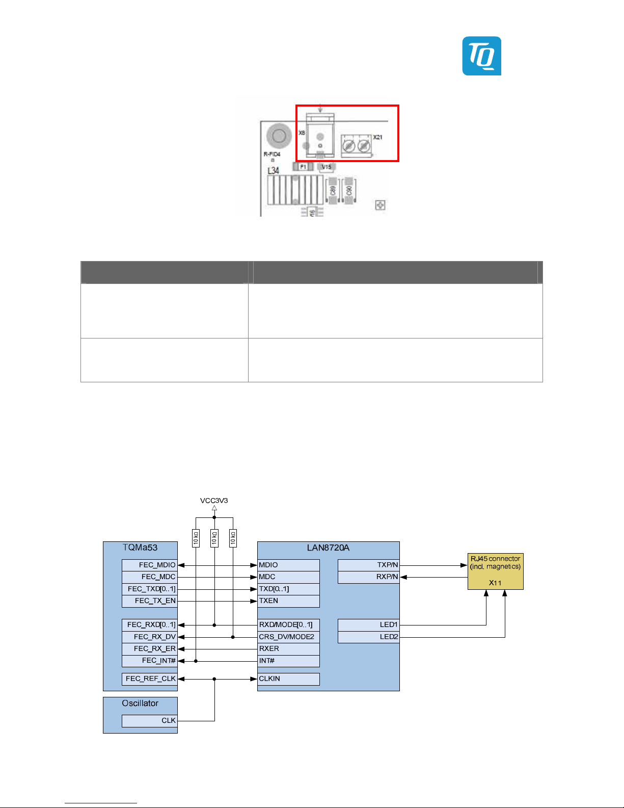
User's Manual l STK-MBa53 UM 100 l © 2013 TQ-Group Page 21
4.1.7.2 Connector and pin assignment
Illustration 14: Position of power-supply connectors X8, X21
Table 24: Power supply connectors X8, X21
Manufacturer / number Description
CUI INC / PJ-102BH
• DC jack 2.5 mm / 5.5 mm
• Right angle
• Nominal values: 5 A / 24 V
• 5,000 mating cycles
• –25 °C to +85 °C
Lumberg / KRM2
• Screw terminal 5 mm
• Nominal values: 15 A / 240 V (AC)
• Max. cable cross-section 2.5 mm
• –25 °C to +100 °C
4.2
4.24.2
4.2 Communication and supply interfaces
Communication and supply interfacesCommunication and supply interfaces
Communication and supply interfaces
4.2.1 Ethernet 1
The following illustration shows the wiring of the Ethernet 1 interface.
It is designed as a 100Base-TX interface and corresponds to the IEEE 802.3 standard.
The PHY used provides an Auto-MDI-X detection.
The maximum cable length at 100 Mbit/s is 100 m.
An oscillator is provided as a clock generator for the LAN8720 (CLKIN) and the signal FEC_REF_CLK of the TQMa53.
Illustration 15: Block diagram Ethernet 1

User's Manual l STK-MBa53 UM 100 l © 2013 TQ-Group Page 22
The operation mode of the LAN8720A is preconfigured with MODE[2:0] = 111 (all capable).
Other configurations can be set by placement options:
Table 25: LAN8720A modes
MODE [0..2] Function Remark
000 10BASE-T Half-duplex, autonegotiation off
001 10BASE-T Full-duplex, autonegotiation off
010 10BASE-TX Half-duplex, autonegotiation off
011 100BASE-TX Full-duplex, autonegotiation off
100 100BASE-TX Half-duplex start, autonegotiation on
101 100BASE-TX Repeater Mode, Half-duplex start, autonegotiation on
110 Power down Information in the data sheet
111
111111
111 ALL capable
ALL capableALL capable
ALL capable No definitions
No definitionsNo definitions
No definitions, autonegotiation on,
, autonegotiation on,, autonegotiation on,
, autonegotiation on, preset m
preset mpreset m
preset mode in
ode in ode in
ode in hardware
hardwarehardware
hardware
The RJ45 receptacle X11 provides 2 status LEDs, as well as an integrated magnetics.
Illustration 16: Position of Ethernet connector X11
Table 26: Ethernet connector X11
Manufacturer / number Description
Pulse / J0011D21BNL
• RJ45 receptacle
• Integrated magnetics
• 1.5 kV RMS (min.)
• LEDs: green and yellow
• 0 °C to +70 °C
• 750 mating cycles
Table 27: Pin assignment RJ45 receptacle X11 (Ethernet 1)
Pin Pin name Signal Dir. Remark
1 TX+ ETH1_TXP O –
2 TX– ETH1_TXN O –
3 RX+ ETH1_RXP I –
4 – VCC3V3A_ETH1 – –
5 – – – –
6 RX– ETH1_RXN I –
7 n.c. – – (Not used)
8 – DGND P –
M1..2 – DGND P –
A1 (12) LED1 anode (+) VCC3V3A_ETH1 –
Link Activity, green (shines with available
connection, blinks with transfer)
K1 (11) LED1 cathode (–) INTSEL# (270 Ω) –
A2 (9) LED2 anode (+) REGOFF –
Speed Indicator, yellow (shines with
100 Mbit/s, does not shine with 10 Mbit/s)
K2 (10) LED2 cathode (–) DGND (270 Ω) –
# - low active signal, - element to VCC5V (pull-up), - element to ground (pull-down), - element in series

User's Manual l STK-MBa53 UM 100 l © 2013 TQ-Group Page 23
4.2.2 Ethernet 2 / USB 2.0 Hi-Speed Host
A USB hub with integrated Ethernet controller provides three USB 2.0 Hi-Speed host interfaces, as well as the second Ethernet
interface. The hub has an upstream USB port, four downstream USB ports and an Ethernet interface.
The wiring is based on the reference schematic of the LAN9514. The 5 V host voltage is activated and the current is monitored in
each case with the power distribution switches for the USB 2.0 hosts. In case of an overload and / or excessive heat they switch
off the host voltage. The LAN9514 is clocked by an external 25 MHz oscillator7.
USB host 1 and 2 are routed to the dual port USB receptacle X9. USB host 3 is routed on header X19.
The RJ45 receptacle X10 provides two status LEDs as well as an integrated magnetics.
Illustration 17: Block diagram USB 2.0 Hi-Speed 1 – 3, Ethernet 2
7
±50 ppm (incl. tolerance at 25 °C, drift over temperature range of –40 °C to +85 °C and ageing after 10 years).

User's Manual l STK-MBa53 UM 100 l © 2013 TQ-Group Page 24
Illustration 18: Position of USB, RJ45, pin header, connectors X9, X10, X19
The pin assignment of connectors X9, X10 and X19 is shown in Table 29, Table 30 and Table 31.
Table 28: USB, RJ45, pin header, connectors X9, X10, X19
Connector Manufacturer / number Description
X9 Yamaichi / USB-A-002A
• Dual port USB receptacle, type USB-A
• U
N
=30 V
RMS
AC / IN = 1 A
• U
max
=500 V AC for 1 minute
• –55 °C to +85 °C
X10 Pulse / J0011D21BNL
• RJ45 receptacle
• Integrated magnetics
• 1.5 kV
RMS
(min.)
• LEDs: green and yellow
• 0 °C to +70 °C
• 750 mating cycles
X19 Fischer Elektronik / SL 22 124 60 G
• Pin header 2.54 mm pitch
• 2 × 30 pins
• >7 N retention force
• –40 °C to +163 °C

User's Manual l STK-MBa53 UM 100 l © 2013 TQ-Group Page 25
Table 29: Pin assignment USB host 1 / 2 connector X9
Pin Pin name Signal Dir. Remark
U1_1 VBUS USB_HOST1_VBUS (EMI filter ) P 100 µF to DGND
U1_2 D– USBH1_D– I/O Additional common mode choke in series
U1_3 D+ USBH1_D+ I/O Additional common mode choke in series
U1_4 Ground DGND P –
M1 – DGND P –
U2_1 VBUS USB_HOST2_VBUS (EMI filter ) P 100 µF to DGND
U2_2 D– USBH2_D– I/O Additional common mode choke in series
U2_3 D+ USBH2_D+ I/O Additional common mode choke in series
U2_4 Ground DGND P –
M18 – DGND P –
# - low active signal, - element to VCC5V (pull-up), - element to ground (pull-down), - element in series
Table 30: Pin assignment RJ45 receptacle X10 (Ethernet 2)
Pin Name Signal Dir. Remark
1 TX+ ETH2_TXP O –
2 TX– ETH2_TXN O –
3 RX+ ETH2_RXP I –
4 – VCC3V3A_ETH2 (10 Ω) – –
5 – VCC3V3A_ETH2 (10 Ω) – –
6 RX– ETH2_RXN I –
7 n.c. n.c. – (Not used)
8 – DGND P –
M1..2 – DGND P –
A1 (9) LED1 Anode VCC3V3 –
Link Activity, green
(shines when connection is established, blinks during transfer)
K1 (10) LED1 Cathode ETH2_LINKA# (270 Ω) –
A2 (12) LED2 Anode VCC3V3 –
Speed Indicator, yellow
(shines at 100 Mbit/s, does not shine at 10 Mbit/s)
K2 (11) LED2 Cathode ETH2_SPD# (270 Ω) –
# - low active signal, - element to VCC5V (pull-up), - element to ground (pull-down), - element in series
Table 31: Pin assignment USB host 3 pin header X19
Pin Signal Dir. Remark
34 USBH3_VBUS P 100 µF to DGND
36 USBH3_D– I/O Additional common mode choke in series
38 USBH3_D+ I/O Additional common mode choke in series
# - low active signal, - element to VCC5V (pull-up), - element to ground (pull-down), - element in series
8
See USB-Host 1.

User's Manual l STK-MBa53 UM 100 l © 2013 TQ-Group Page 26
4.2.3 USB 2.0 Hi-Speed OTG
The USB-OTG interface of the TQMa53 is provided on the STK-MBa53. The OTG compatibility is achieved by a 5-pin Micro-AB
receptacle.
The ID signal is directly routed to the CPU. USB 2.0 has been implemented, which works in the Hi-Speed, Full-Speed or LowSpeed mode.
Illustration 19: Block diagram USB 2.0 Hi-Speed OTG
Illustration 20: Position of USB Micro-AB connector X16
Table 32: USB type Micro-AB connector X16
Manufacturer / number Description
Tyco / 1981584-1
• USB receptacle, type Micro-AB
• Right angle
• 10,000 mating cycles
• –30 °C to +85 °C
Table 33: Pin assignment USB OTG connector X16
Pin Pin name Signal Dir. Remark
1 VBUS USB_OTG_VBUS (EMI Filter ) P 100 µF to DGND, IIII
max
maxmax
max
= 100 mA
= 100 mA= 100 mA
= 100 mA
2 D– USBOTG_D– I/O Additional common mode choke in series and bidirectional ESD-diode
3 D+ USBOTG_D+ I/O Additional common mode choke in series and bidirectional ESD-diode
4 ID USB_OTG_ID I –
5 Ground DGND P –
M1..6 – DGND P –
# - low active signal, - element to VCC5V (pull-up), - element to ground (pull-down), - element in series

User's Manual l STK-MBa53 UM 100 l © 2013 TQ-Group Page 27
4.2.4 CAN1 / CAN2
Illustration 21: Block diagram CAN1/CAN2
Both CAN interfaces of the STK-MBa53 are directly connected to the CAN ports of the TQMa53. They are available at the 3-pin
plug connectors X3 and X4. Both interfaces are galvanically separated from the rest of the circuitry. The two CAN interfaces are,
however, not galvanically separated from each other.
The high speed mode is configured at the input RS of the CAN transceivers MCP2551 by default. R24 configures CAN1 and R30
configures CAN2. The two 390 Ω resistors to ground ensure maximum slew rate. The high-speed mode supports data rates of up
to 1 Mbit/s or maximum cable lengths. To reduce the slew rate the resistance at RS can be increased (10 kΩ to 120 kΩ), if required.
The CAN signals can be terminated with 120 Ω using DIP switches S10–1 and S10–2. More information can be found in the
following section.
Table 34: Electrical parameter CAN1 / CAN2
Parameter Min. Typ. Max. Unit Remark
Transfer rate – – tbd baud –
Line length – – tbd m 10 Mbaud
Line length – – tbd m 500 kbaud
Output voltage CANH (dominant / high) 2.75 – 4.5 V –
Output voltage CANL (dominant / high) 0.5 – 2.25 V –
Output voltage CANH / CANL (recessive) 2 – 3 V Without load
Output voltage differential recessive –500 – 50 mV Without load
Output voltage differential dominant 0.5 – 2.25 V –
The interfaces CAN1 and CAN2 can be terminated with DIP switches S10–1 / S10–2.
The configuration of the DIP switches is shown in the following table.
Table 35: Settings of DIP switches for CAN1 / CAN2 termination
Switch Interface Position “On” Position “Off”
S10–1 CAN1 CAN1 terminated with 120 Ω CAN1 not terminated
S10–2 CAN2 CAN2 terminated with 120 Ω CAN2 not terminated

User's Manual l STK-MBa53 UM 100 l © 2013 TQ-Group Page 28
Illustration 22: Position of S10
4.2.4.1 Galvanic separation
The characteristics of the galvanic separation are shown in Table 36.
Table 36: Characteristics of the galvanic separation for CAN1 and CAN2
Parameter Min. Typ. Max. Unit
Voltage firmness – – tbd mV
Isolation distance on inner layers 1.1 – – mm
Isolation distance on outer layers 1.7 – – mm

User's Manual l STK-MBa53 UM 100 l © 2013 TQ-Group Page 29
4.2.4.2 Connectors and pin assignment
Illustration 23: Position of pin headers X3, X4
Table 37: Pin headers X3, X4
Manufacturer / number Description
Phoenix Contact / MCV 1,5/ 3-G-3,5
• 3-pin header
• 160 V / 8 A
• Pitch: 3.5 mm
• –40 °C to +100 °C
Table 38: Pin assignment CAN1 / CAN2 connector X3, X4
Pin Pin name / signal Dir. Remark
X3-1 CAN1_H I/O CAN High-Level I/O, galvanically separated
X2-2 CAN1_L I/O CAN Low-Level I/O, galvanically separated
X3-3 DGND_CAN P Galvanically separated
X4-1 CAN2_H I/O CAN High-Level I/O, galvanically separated
X4-2 CAN2_L I/O CAN Low-Level I/O, galvanically separated
X4-3 DGND_CAN P Galvanically separated
Pin X3
-1
Pin X4-1

User's Manual l STK-MBa53 UM 100 l © 2013 TQ-Group Page 30
4.2.5 RS232
Illustration 24: Block diagram RS232
UART2 of the i.MX53 is routed to the transceiver SP3222E, which provides the signals as RS232 interface at a D-Sub 9-pin
connector according to the EIA/TIA-232-F standard. The UART2 handshake signals RTS# and CTS# are also available.
The UART2 interface is used as debug information output.
Further information (e.g.: default baud rate) should be taken from the software specification.
Table 39: Electrical parameters RS232
Parameter Min. Typ. Max. Unit Remark
Transfer rate – – tbd baud –
Line length – – tbd m 235,000 baud
Line length – – tbd m 115,200 baud
Line length – – tbd m 96,000 baud
Output voltage Low – – 0.4 V I
out
1.6 mA
Output voltage High 2.7 – – V –
Illustration 25: Position of D-Sub 9-pin connector X1

User's Manual l STK-MBa53 UM 100 l © 2013 TQ-Group Page 31
Table 40: D-Sub 9-pin connector X1
Manufacturer / number Description Package
Yamaichi / DRA-09P11-ZN
• D-Sub connector
• 9-pin
• Right angle
• –55 °C to +105 °C
THT9
Table 41: Pin assignment RS232 connector X1
Pin Pin name Signal Dir. Remark
1 n.c. – – (Not used)
2 RXD RS232_RXD I –
3 TXD RS232_TXD O –
4 n.c. – – (Not used)
5 GND DGND P –
6 n.c. – – (Not used)
7 RTS# RS232_RTS# O –
8 CTS# RS232_CTS# I –
9 n.c. – – (Not used)
M1 – DGND P –
4.2.6 RS485
Illustration 26: Block diagram RS485
UART3 of the i.MX53 is routed to the transceiver SP491E, which provides the signals as RS485 interface at the D-Sub 9-pin
connector X2. The RS485 interface is galvanically separated and can operate in Full-duplex mode at a maximum of 10 Mbit/s.
Half-duplex mode is also possible by placement option.
Table 42: Configuration of the RS485 modes
Mode R10 R11 Remark
Full-duplex n.a. 0 Ω Receiver always active (default)
Half-duplex 0 Ω n.a. Receiver is controlled by DE_Signal (GPIO1_GPIO3)
The RS485 signals can be terminated with 120 Ω by using DIP switches S4–1 and S4–2.
Details can be found in the following section.
The DC/DC converter R1S-0505 provides an isolation voltage of 1 kV. It does not provide short circuit protection.

User's Manual l STK-MBa53 UM 100 l © 2013 TQ-Group Page 32
Table 43: Electrical parameters RS485
Parameter Min. Typ. Max. Unit Remark
Transfer rate – – tbd baud
Line length – – tbd m 10 Mbaud
Line length – – tbd m 115,200 baud
Line length – – tbd m 96,000 baud
Output voltage Low – – 0.4 V I
out
= +4 mA
Output voltage High 3.5 – – V I
out
= –4 mA
The RS485 signals can be terminated with 120 Ω using DIP switches S4–1 and S4–2.
The possible settings of the DIP switches are shown in the following table.
Table 44: Settings of DIP switch S4 for RS485
Switch Interface Position “On” Position “Off”
S4–1 RS485 Receive path is terminated with 120 Ω Receive path is not terminated
S4–2 RS485 Transmit path is terminated with 120 Ω Transmit path is not terminated
Illustration 27: Position of pin headers S4

User's Manual l STK-MBa53 UM 100 l © 2013 TQ-Group Page 33
The characteristics of the galvanic separation are shown in the following table.
Table 45: Characteristics of the galvanic separation for RS485
Parameter Min. Typ. Max. Unit
Dielectric strength – – tbd V
Isolation distance auf inner layers 1.2 – – mm
Isolation distance auf outer layers 1.7 – – mm
Illustration 28: Position of pin header X2
Table 46: Pin headers connector X2
Manufacturer / number Description
Phoenix Contact / MCV 1,5/ 4-G-3,5
• 4-pin header
• 160 V / 8 A
• Pitch: 3.5 mm
• –40 °C to +100 °C
Table 47: Pin assignment RS485 connector X2
Pin Pin name / signal Dir. Remark
1 RS485_A I Non-inverted input, galvanically separated
2 RS485_B I Inverted input, galvanically separated
3 RS485_Y O Non-inverted output, galvanically separated
4 RS485_Z O Inverted output, galvanically separated
Pin 1

User's Manual l STK-MBa53 UM 100 l © 2013 TQ-Group Page 34
4.2.7 DVI
An external display can be connected to the single link DVI interface, which provides analog and digital image data.
A DVI receptacle type I is used (X5). The DVI interface corresponds to the DVI specification 1.0.
The Transmitter TFP410 for the digital image signals provides two possibilities to configure the display interface:
• By IC bus
• By fixed wiring using the config pins
On the STK-MBa53 the configuration by IC is used by default.
The display interface can also be configured using configuration resistors as a placement option.
Detailed information concerning the component placement options is to be taken from the circuit diagram.
Resolutions of up to 1080p and WUXGA at 60 Hz or pixel rates of up to 165 MHz are supported.
More details are to be taken from the TFP410 data sheet.9
The VGA signals for RGB are directly routed to the connector.
The levels of the following signals are separately adapted to the VESA standard:
• VGA_HSYNC and VGA_VSYNC
• I2C3_SCL and I2C3_SDA
The levels are adapted using the VGA Port Protector MAX4895E.
This device also provides an ESD protection for the RGB signals.
Some of the image data signals are used to configure the boot-mode and are routed to header X19, too.
Illustration 29: Block diagram DVI (analog signals)
9
See (8), data sheet TFP410.

User's Manual l STK-MBa53 UM 100 l © 2013 TQ-Group Page 35
By using a DVI-I receptacle, which transmits digital and analog image signals, the interface is compatible to the VGA standard
and to the HDMI standard. The difference to the HDMI standard is that with DVI only video and no audio signals are transmitted.
Illustration 30: Block diagram DVI (digital signals)
Illustration 31: Position of DVI connector X5
Table 48: DVI connector X5
Manufacturer / No. Description Package
Molex / 74320-1004
• DVI-I receptacle
• Right angle
• 100 mating cycles
• –20 °C to +85 °C
THT30

User's Manual l STK-MBa53 UM 100 l © 2013 TQ-Group Page 36
Table 49: Pin assignment DVI connector X5
Pin Pin name Signal Dir. Remark
1 TMDS Data2– TMDS_DATA2– O Additional data line filter in series
2 TMDS Data2+ TMDS_DATA2+ O Additional data line filter in series
3 TMDS Data2/4 Shield DGND P –
4 TMDS Data4– n.c. – (Not used)
5 TMDS Data4+ n.c. – (Not used)
6 DDC Clock DDC_CLK O 15 k Ωto VCC5V, additional LCL filter in series
7 DDC Data DDC_SDA I/O 15 k Ω to VCC5V, additional LCL filter in series
8 Analog Vsync ANALOG_VSYNC O –
9 TMDS Data1– TMDS_DATA1– O Additional data line filter in series
10 TMDS Data1+ TMDS_DATA1+ O Additional data line filter in series
11 TMDS Data1/3 Shield DGND P –
12 TMDS Data3– n.c. – (Not used)
13 TMDS Data3+ n.c. – (Not used)
14 +5V Power VCC5V P IIII
max
max max
max
= 55 mA
= 55 mA= 55 mA
= 55 mA, 10 µF, 1 µF to DGND, additional LCL-Filter in series
15 Ground DGND P –
16 Hot Plug Detect HOTPLUG_DETECT (1 kΩ) I Additional LCL filter in series
17 TMDS Data0– TMDS_DATA0– O Additional data line filter in series
18 TMDS Data0+ TMDS_DATA0+ O Additional data line filter in series
19 TMDS Data0/5 Shield DGND P –
20 TMDS Data5– n.c. – (Not used)
21 TMDS Data5+ n.c. – (Not used)
22 TMDS Clock Shield DGND P –
23 TMDS Clock+ TMDS_CLK+ (270 Ω || TMDS_CLK–) O Additional data line filter in series
24 TMDS Clock– TMDS_CLK– O Additional data line filter in series
C1 Analog Red ANALOG_RED O 75 Ω to AGND_VGA, additional ferrite filter in series
C2 Analog Green ANALOG_GREEN O 75 Ω to AGND_VGA, additional ferrite filter in series
C3 Analog Blue ANALOG_BLUE O 75 Ω to AGND_VGA, additional ferrite filter in series
C4 Analog Hsync ANALOG_HSYNC O –
C5a/b Analog Ground AGND_VGA P –
M1..2 – DGND P –
# - low active signal, - element to VCC5V (pull-up), - element to ground (pull-down), - element in series

User's Manual l STK-MBa53 UM 100 l © 2013 TQ-Group Page 37
4.2.8 LVDS
Both LVDS interfaces of the TQMa53 (one pair of clock signals and four pair of data signals each) are routed directly to the 30-pin
female connector X17.
In addition to the LVDS signals 3.3 V and 5 V are provided at the connector. The current drawn from this connector, including the
current drawn from header X19 and "Power-out", X20, may not exceed 1 A for each voltage.
The STK-MBa53 was qualified with the AUO display G156XW01 v.1.
Illustration 32: Block diagram LVDS
Illustration 33: Position of LVDS connector X17
Pin 1
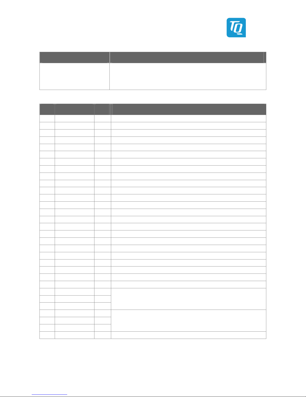
User's Manual l STK-MBa53 UM 100 l © 2013 TQ-Group Page 38
Table 50: LVDS connector X17
Manufacturer / number Description
Hirose / DF19G-30P-1H
• Board to cable socket connector 30-pin
• Pitch: 1 mm
• Right angle
• 30 mating cycles
30 mating cycles30 mating cycles
30 mating cycles
• –35 °C to +85 °C
Table 51: Pin assignment LVDS header X17
Pin Pin name / signal Dir. Remark
1 LVDS0_TX0_N O
2 LVDS0_TX0_P O
3 LVDS0_TX1_N O
4 LVDS0_TX1_P O
5 LVDS0_TX2_N O
6 LVDS0_TX2_P O
7 DGND P
8 LVDS0_CLK_N O
9 LVDS0_CLK_P O
10 LVDS0_TX3_N O
11 LVDS0_TX3_P O
12 LVDS1_TX0_N O
13 LVDS1_TX0_P O
14 DGND P
15 LVDS1_TX1_N O
16 LVDS1_TX1_P O
17 DGND P
18 LVDS1_TX2_N O
19 LVDS1_TX2_P O
20 LVDS1_CLK_N O
21 LVDS1_CLK_P O
22 LVDS1_TX3_N O
23 LVDS1_TX3_P O
24 DGND P
25 VCC5V_LVDS P
IIII
max
maxmax
max
= 1 A
= 1 A= 1 A
= 1 A
((((minus the current, which is drawn from the headers X19 and "Power
minus the current, which is drawn from the headers X19 and "Powerminus the current, which is drawn from the headers X19 and "Power
minus the current, which is drawn from the headers X19 and "Power----OUT" (X20))
OUT" (X20))OUT" (X20))
OUT" (X20))
10 µF, 1 µF to DGND, additional ferrite filters in series
26 VCC5V_LVDS P
27 VCC5V_LVDS P
28 VCC3V3_LVDS P
IIII
max
maxmax
max
= 1 A
= 1 A= 1 A
= 1 A
((((minus the current, which is drawn from the headers X19 and "Power
minus the current, which is drawn from the headers X19 and "Powerminus the current, which is drawn from the headers X19 and "Power
minus the current, which is drawn from the headers X19 and "Power----OUT" (X20))
OUT" (X20))OUT" (X20))
OUT" (X20))
10 µF, 1 µF to DGND, additional ferrite filters in series
29 VCC3V3_LVDS P
30 VCC3V3_LVDS P
M1..2 DGND P
# - low active signal, - element to VCC5V (pull-up), - element to ground (pull-down), - element in series
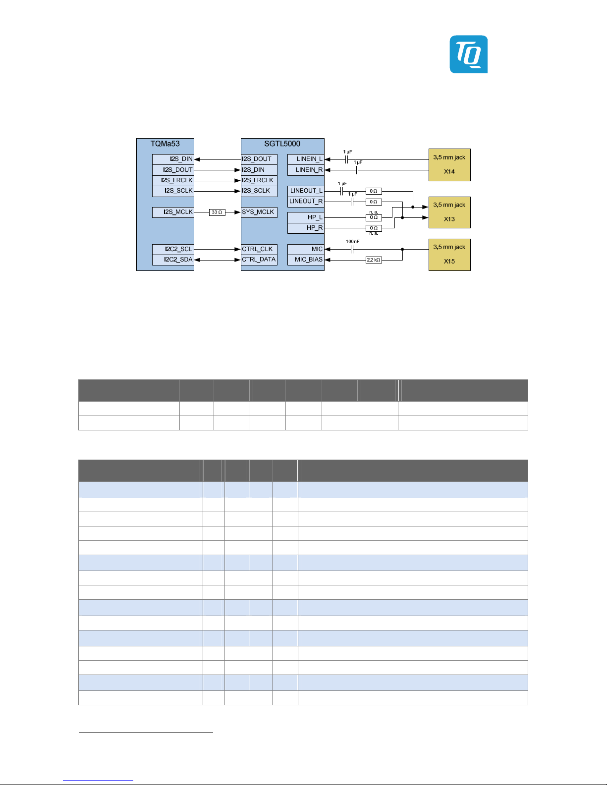
User's Manual l STK-MBa53 UM 100 l © 2013 TQ-Group Page 39
4.2.9 Audio
To process audio input and output signals the audio-codec SGTL5000 is provided.
It is connected to the TQMa53 over the interfaces IC and IS. The IC bus 2 is used.
Illustration 34: Block diagram audio
The SGTL500010 provides a stereo line-in, stereo line-out, a microphone input, as well as an (amplified) headphone output.
The headphone output is, however, not available on the STK-MBa53 by default. It can be enabled at X13 by placement option.
The necessary configurations are shown in Table 52.
The audio interfaces are provided at three 3.5 mm jacks (X13 – X15). The basic electric characteristics are shown in Table 53.
Table 52: Configuration for headphone or line-out
Signals at X13 R112 R114 R113 R115 R117 R118 Remark
Line-out 0 Ω 0 Ω n.a. n.a. 0 Ω n.a. Default
Headphone n.a. n.a. 0 Ω 0 Ω n.a. 0 Ω
Table 53: Electric characteristics of the audio interface
Parameter Min. Typ. Max. Unit Remark
Headphone (p
Headphone (pHeadphone (p
Headphone (placement option
lacement optionlacement option
lacement option)))) Stereo
StereoStereo
Stereo
Output power – – 58 mW At 16 Ω input impedance
Output power – – 30 mW At 32 Ω input impedance
Signal-noise ratio – – 98 dB At 16 Ω input impedance, with –60 dB input power
Signal-noise ratio – – 100 dB At 32 Ω input impedance, with –60 dB input power
Line
LineLine
Line----out
outout
out Stereo
StereoStereo
Stereo
Signal-noise ratio – – 100 dB With –60 dB input power
Output level – – 1 V
RMS
–
Line
LineLine
Line----in
inin
in Stereo
StereoStereo
Stereo
Input impedance 10 – – kΩ –
Microphone input
Microphone inputMicrophone input
Microphone input Mono
MonoMono
Mono
Gain – N*10 – dB N = [0, 2, 3, 4]
1.25 – 3 V Can be set in steps of 0.25 V
General
GeneralGeneral
General
Sampling rate 8 – 96 kHz Only multiples of SYS_MCLK (256×, 384×, 512×) can be selected
10
See (6), data sheet SGTL5000.
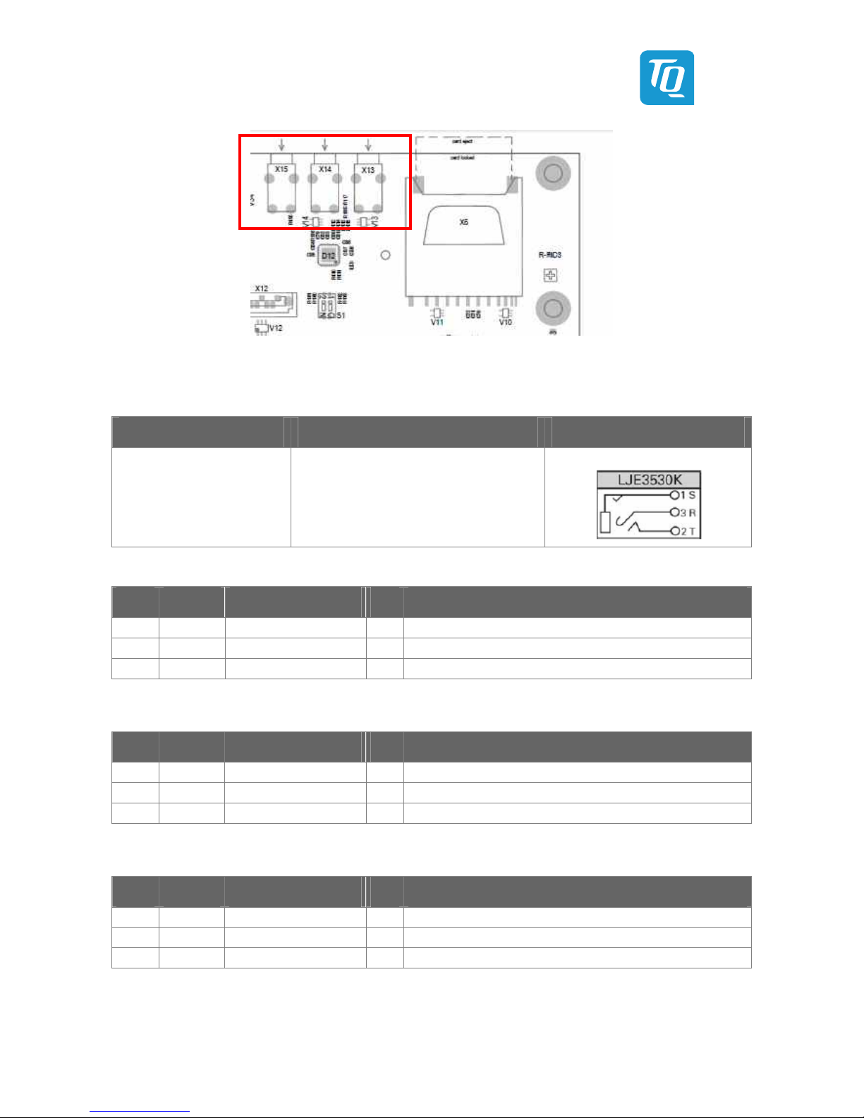
User's Manual l STK-MBa53 UM 100 l © 2013 TQ-Group Page 40
Illustration 35: Position of jacks X13, X14, X15
Table 54: Jacks X13, X14, X15
Manufacturer / number Description Package
Yamaichi / LJE3530K
• Jack, 3.5 mm
• Right angle
• 5,000 mating cycles
• Contact resistance: 30 mΩ (max.)
THT4
Table 55: Pin assignment audio connector X13 (line-out / headphone)
Pin Pin name Signal Dir. Remark
1 Ground AGND_AUDIO P Optional connection to AGND_HP (0 Ω, n.a.)
2A, 2B Left AUDIO_OUT_L (1 µF) AO Optional connection to HP_L (0 Ω, n.a.), additional ESD protection
3 Right AUDIO_OUT_R (1 µF) AO Optional connection to HP_R (0 Ω, n.a.), additional ESD protection
# - low active signal, - element to VCC5V (pull-up), - element to ground (pull-down), - element in series
Table 56: Pin assignment audio connector X14 (line-in)
Pin Pin name Signal Dir. Remark
1 Ground AGND_AUDIO P –
2A, 2B Left AUDIO_IN_L (1 µF) AI Additional ESD protection
3 Right AUDIO_IN_R (1 µF) AI Additional ESD protection
# - low active signal, - element to VCC5V (pull-up), - element to ground (pull-down), - element in series
Table 57: Pin assignment audio connector X15 (microphone)
Pin Pin name Signal Dir. Remark
1 Ground AGND_AUDIO P –
2A, 2B Left MIC_IN (100 nF) AI 2.2 kΩ MIC_BIAS, additional ESD protection
3 Right AGND_AUDIO (10 kΩ) AI (Not used, only mono)
# - low active signal, - element to VCC5V (pull-up), - element to ground (pull-down), - element in series

User's Manual l STK-MBa53 UM 100 l © 2013 TQ-Group Page 41
4.2.10 SD card
Illustration 36: Block diagram SD card
The SD card connector is directly routed to the SDHC controller of the TQMa53. All signals are equipped with an additional ESD
protection near the card connector. It is possible to boot from SD card (see section 4.3.5, Boot-Mode configuration).
Illustration 37: Position of SD card connector X6
Table 58: SD card connector X6
Manufacturer / number Description
Yamaichi / FPS009-2405-0
• SD / MMC card connector
• 10,000 mating cycles
• Push/Push latch
• –25 °C to +85 °C
Table 59: Pin assignment SD card connector X6
Pin Pin name Signal Dir. Remark
1 DAT3 / CS SD_DAT3 I/O 10 kΩ to VCC3V3 (n.a.), additional ESD protection
2 CMD / DATA IN SD_CMD I/O 10 kΩ to VCC3V3, additional ESD protection
3 VSS1 DGND P –
4 VDD VCC3V3 P 1 µF / 100 nF / 10 nF to DGND
5 CLK SD_CLK_R (22 Ω) O Additional ESD protection
6 VSS2 DGND P –
7 DAT0 / DATA OUT SD_DAT0 I/O 10 kΩ to VCC3V3 (n.a.), additional ESD protection
8 DAT1 SD_DAT1 I/O 10 kΩ to VCC3V3 (n.a.), additional ESD protection
9 DAT2 SD_DAT2 I/O 10 kΩ to VCC3V3 (n.a.), additional ESD protection
WP WRITE_PROTECT SD_WP I 10 kΩ to VCC3V3, additional ESD protection
CD CARD_DETECT# SD_CD# I 10 kΩ to VCC3V3, additional ESD protection
GND COMMON DGND P –
M1..2 – DGND P –
# - low active signal, - element to VCC5V (pull-up), - element to ground (pull-down), - element in series

User's Manual l STK-MBa53 UM 100 l © 2013 TQ-Group Page 42
4.2.11 SATA
Illustration 38: Block diagram SATA-Interface
The SATA interface of the TQMa53 is capacitive coupled (10 nF) to a 7-pin SATA connector.
The SATA device must be supplied separately, e.g., over the Power-Out header X20.
All four data lines have an ESD protection.
It is possible to boot from SATA, see section 4.3.5, Boot-Mode configuration.
The SATA interface provides the following core functionalities11:
• Compatible with Serial ATA 2.6, AHCI Revision 1.3
12
and AMBA 2.0 (ARM)
• Data rate of 1.5 Gbit/s
Illustration 39: Position of SATA connector X12
Table 60: SATA connector X12
Manufacturer / number Description
3M / 5607-5102-SH
• SATA connector 7-pin
• Vertical version
• Corresponds to SATA specification
• –40 °C to +85 °C
Table 61: Pin assignment SATA connector X12
Pin Pin name Signal Dir. Remark
1 Ground DGND P –
2 A+ SATA_TX+ (10 nF) I Additional ESD protection
3 A– SATA_TX– (10 nF) I Additional ESD protection
4 Ground DGND P –
5 B– SATA_RX– (10 nF) O Additional ESD protection
6 B+ SATA_RX+ (10 nF) O Additional ESD protection
7 Ground DGND P –
M1, M2 – DGND – –
# - low active signal, - element to VCC5V (pull-up), - element to ground (pull-down), - element in series
11
See (2), i.MX53 multimedia Applications Processor Reference Manual.
12
No FIS switching.

User's Manual l STK-MBa53 UM 100 l © 2013 TQ-Group Page 43
4.2.12 JTAG
Illustration 40: Block diagram JTAG
The JTAG interface is routed to the 20-pin header X7.
The pull-up and pull-down resistors for the signals TDI, TMS, TRST# and TCK are assembled on the TQMa53.
The reference of 2.775 V provided by the TQMa53 is used as I/O voltage.
This causes deviant high and low levels for the corresponding signals, see Table 62.
Table 62: High- and Low level for 2.775V signals of the JTAG interface
Parameter Min. Typ. Max. Unit
High level output voltage 2.2 – – V
Low level output voltage – – 0.555 V
High level input voltage 1.9425 – 2.775 V
Low level input voltage 0 – 0.8325 V
The reference voltage VCC _2V775 may not be used as a supply voltage.
VCC3V3 is also routed to the pin header. The maximum load is 10 mA.
The JTAG interface on the STK-MBa53 has no ESD protection.
Illustration 41: Position of pin header X7
Pin 1

User's Manual l STK-MBa53 UM 100 l © 2013 TQ-Group Page 44
Table 63: Pin header X7
Manufacturer / number Description
Fischer Elektronik / SL 11 SMD 052 20 G
• Header 2.54 mm pitch
• 2 × 10 pins
• >7 N retention force
• –40 °C to +163 °C
Table 64: Pin assignment JTAG
Pin Pin name Signal Dir. Remark
1 VREF VCC_2V775 (100 Ω) P 100 nF to DGND use only as reference
use only as referenceuse only as reference
use only as reference
2 VSUPPLY VCC3V3 (0 Ω) P 100 nF to DGND, IIII
max
maxmax
max
= 10 mA
= 10 mA= 10 mA
= 10 mA
3 TRST# JTAG_TRST# I On the TQMa53: 10 kΩ to VCC2V775
4 GND DGND P –
5 TDI JTAG_TDI I On the TQMa53: 10 kΩ to VCC2V775
6 GND DGND P –
7 TMS JTAG_TMS I On the TQMa53: 10 kΩ to VCC2V775
8 GND DGND P –
9 TCK JTAG_TCK I On the TQMa53: 10 kΩ to DGND
10 GND DGND P –
11 GND DGND (10 kΩ) I –
12 GND DGND P –
13 TDO JTAG_TDO O –
14 GND DGND P –
15 SRST# RESET_IN# I –
16 GND DGND P –
17 DBGRQ VCC_2V775 (10 kΩ) I –
18 GND DGND P –
19 DBGACK DGND (10 kΩ) I –
20 GND DGND P –
# - low active signal, - element to VCC5V (pull-up), - element to ground (pull-down), - element in series

User's Manual l STK-MBa53 UM 100 l © 2013 TQ-Group Page 45
4.2.13 Pin headers
To connect extension cards to the STK-MBa53 all unused and some other selected signals are routed to pin headers X18, X19 and
X20. All pin headers have 60 pins with a 2.54 mm pitch.
The close placement of the headers makes it easy to plug on self-developed boards.
Illustration 42: Position of pin headers 18, X19, X20
Table 65: Pin headers X18, X19, X20
Manufacturer / number Description
Fischer Elektronik / SL 22 124 60 G
• Header 2.54 mm pitch
• 2 × 30 pins
• >7 N retention force
• –40 °C to +163 °C
The following tables show the distribution of the function groups at the three pin headers.
Pin 1

User's Manual l STK-MBa53 UM 100 l © 2013 TQ-Group Page 46
Table 66: Pin header X18
Pin
PinPin
Pin Signal
SignalSignal
Signal Interface TQMa53
Interface TQMa53Interface TQMa53
Interface TQMa53 Dir.
Dir.Dir.
Dir.
Remark:
Remark:Remark:
Remark:
1: Alternative function WEIM bus
2: Routed to DVI transmitter
3: Used for Boot-Mode configuration
1 DGND – Power 2
DGND – Power 3
CSI0_MCLK
CSI0 O 4
CSI0_HSYNC
CSI0 I 5
CSI0_PIXCLK
CSI0 I 6
CSI0_VSYNC
CSI0 I 7
DGND – Power 8
DGND – Power 9
CSI0_DATA_EN
CSI0 I 10
CSI0_D4
CSI0 I 11
CSI0_D5
CSI0 I 12
CSI0_D6
CSI0 I 13
CSI0_D7
CSI0 I 14
CSI0_D8
CSI0 I 15
CSI0_D9
CSI0 I 16
CSI0_D10
CSI0 I 17
CSI0_D11
CSI0 I 18
CSI0_D12
CSI0 I 19
CSI0_D13
CSI0 I 20
CSI0_D14
CSI0 I 21
CSI0_D15
CSI0 I 22
CSI0_D16
CSI0 I 23
CSI0_D17
CSI0 I 24
CSI0_D18
CSI0 I 25
CSI0_D19
CSI0 I 26
CSI0_PWDN
CSI0 O 27
GPIO3_GPIO20
GPIO I/O 1 28 CSI0_RST#
CSI0 O 29
GPIO3_GPIO29
GPIO I/O 1 30 GPIO3_GPIO28
GPIO I/O 1 31 GPIO3_GPIO21
GPIO I/O 1 32 GPIO3_GPIO22
GPIO I/O 1 33 GPIO2_GPIO27
GPIO I/O 1, 3 34 GPIO2_GPIO26
GPIO I/O 1 35 GPIO2_GPIO23
GPIO I/O 1 36 GPIO2_GPIO25
GPIO I/O 1 37 GPIO3_GPIO13
GPIO I/O 1 38 GPIO3_GPIO11
GPIO I/O 1 39 GPIO3_GPIO14
GPIO I/O 1 40 GPIO5_GPIO0
GPIO I/O 1, In addition, as an interrupt signal of the I/O expander usable
41
GPIO3_GPIO12
GPIO I/O 1 42 ESPI_MISO
ESPI I 1 43 DGND – Power 44
ESPI_MOSI
ESPI O 1 45 ESPI_SS1#
ESPI O 1 46 ESPI_SS2#
ESPI O 1 47 ESPI_SS0#
ESPI O 1 48 FIRI_RXD
FIRI I 49
ESPI_SS3#
ESPI O 1 50 FIRI_TXD
FIRI O 51
ESPI_SCLK
ESPI O 1 52 UART1_RXD
UART1
I 53 OWIRE
1-
wire I/O 54
UART1_TXD
UART1
O 55 I2C3_SCL
I2C3 O Additionally used as on
-
board bus
56
SPDIF_OUT
SPDIF O 57
I2C3_SDA
I2C3 I/O Additionally used as on
-
board bus
58
SPDIF_IN
SPDIF I 59
DGND – Power
60 DGND – Power

User's Manual l STK-MBa53 UM 100 l © 2013 TQ-Group Page 47
Table 67: Pin header X19
Pin
PinPin
Pin Signal
SignalSignal
Signal Interface
InterfaceInterface
Interface Dir.
Dir.Dir.
Dir.
Remark:
Remark:Remark:
Remark:
1: Alternative function WEIM bus
2: Routed to DVI transmitter
3: Used for Boot-Mode configuration
1 VCC12V
–
Power
I
max
= 1 A per voltage
(minus the current drawn from pin header „Power-OUT“
and the LVDS connector)
2 VCC3V3
–
Power 3 VCC5V
–
Power 4 VCC3V3
–
Power 5 DGND – Power 6
DGND – Power 7
DISP1_CLK
DISP1 O 2, 3 8 DISP1_DRDY_DE
DISP1 O 1, 2 9 DISP1_HSYNC
DISP1 O 1, 2 10 DISP1_DAT1
DISP1 O 1, 2, 3 11 DISP1_VSYNC
DISP1 O 1, 2 12 DISP1_DAT3
DISP1 O 1, 2, 3 13 DISP1_DAT0
DISP1 O 1, 2, 3 14 DISP1_DAT5
DISP1 O 1, 2 15 DISP1_DAT2
DISP1 O 1, 2, 3 16 DISP1_DAT7
DISP1 O 1, 2, 3 17 DISP1_DAT4
DISP1 O 1, 2 18 DISP1_DAT9
DISP1 O 1, 2, 3 19 DISP1_DAT6
DISP1 O 1, 2 20 DISP1_DAT11
DISP1 O 2, 3 21 DISP1_DAT8
DISP1 O 1, 2, 3 22 DISP1_DAT13
DISP1 O 2, 3 23 DISP1_DAT10
DISP1 O 2, 3 24 DISP1_DAT15
DISP1 O 2, 3 25 DISP1_DAT12
DISP1 O 26
DISP1_DAT17
DISP1 O 2, 3 27 DISP1_DAT14
DISP1 O 2, 3 28 DISP1_DAT19
DISP1 O 29
DISP1_DAT16
DISP1 O 2, 3 30 DISP1_DAT21
DISP1 O 1, 2 31 DISP1_DAT18
DISP1 O 2 32 DISP1_DAT23
DISP1 O 1, 2 33 DISP1_DAT20
DISP1 O 1, 2 34 USBH3_VBUS
– O
100 µF
to DGND
35
DISP1_DAT22
DISP1 O 1 36 USBH3_D
– – I/O Common mode chokes in series
37
DGND – Power 38
USBH3_D+
–
I/O Common mode chokes in
series 39 I2C2_SCL
I2C2 O Additionally used as on
-
board bus
40
DGND – Power 41
I2C2_SDA
I2C2 I/O Additionally used as on
-
board bus
42
SPI_SS0#
SPI O 43
SPI_MOSI
SPI O 44
SPI_MISO
SPI I 45
SPI_SS1#
SPI O 46
SPI_SCLK
SPI O 47
SPI_SS2
SPI O 48
DGND – Power 49
LCD_POWER_EN
LCD-CTRL O 50
LCD_BLT_EN
LCD-CTRL O 51
LCD_RESET
LCD-CTRL O 52
LCD_CONTRAST
LCD-CTRL O 53
DGND – Power 54
DGND – Power 55
TOUCH_Y1
Touch I 56
TOUCH_X1
Touch I 57
TOUCH_Y2
Touch I 58
TOUCH_X2
Touch I 59
DGND – Power
60 DGND – Power
# - low active signal, - element to VCC5V (pull-up), - element to ground (pull-down), - element in series

User's Manual l STK-MBa53 UM 100 l © 2013 TQ-Group Page 48
Table 68: Pin header „Power-Out“ X20
Pin Signal Interface Dir. Remark
1 VCC3V3
–
Power
I
max
= 1 A per voltage
(minus the current drawn at pin header X19
and at the LVDS connector)
2 DGND – Power 3 VCC3V3
–
Power 4 DGND – Power 5 VCC3V3
–
Power 6 DGND – Power 7 VCC3V3
–
Power 8 DGND – Power 9 VCC3V3
–
Power 10 DGND – Power 11 VCC3V3
–
Power 12 DGND – Power 13 VCC3V3
–
Power 14 DGND – Power 15 VCC3V3
–
Power 16 DGND – Power 17 VCC3V3
–
Power 18 DGND – Power 19 VCC5V
–
Power 20 DGND – Power 21 VCC5V
–
Power 22 DGND – Power 23 VCC5V
–
Power 24 DGND – Power 25 VCC5V
–
Power 26 DGND – Power 27 VCC5V
–
Power 28 DGND – Power 29 VCC5V
–
Power 30 DGND – Power 31 VCC5V
–
Power 32 DGND – Power 33 VCC5V
–
Power 34 DGND – Power 35 VCC5V
–
Power 36 DGND – Power 37 VCC12V
–
Power 38 DGND – Power 39 VCC12V
–
Power 40 DGND – Power 41 VCC12V
–
Power 42 DGND – Power 43 VCC12V
–
Power 44 DGND – Power 45 VCC12V
–
Power 46 DGND – Power 47 VCC12V
–
Power 48 DGND – Power 49 VCC12V
–
Power 50 DGND – Power 51 VCC12V
–
Power 52 DGND – Power 53 VCC12V
–
Power 54 DGND – Power 55 PWRON
Reset I 56
DGND – Power 57
GLBRST#
Reset I 58
DGND – Power 59
RESET_OUT#
Reset O 60
DGND – Power

User's Manual l STK-MBa53 UM 100 l © 2013 TQ-Group Page 49
4.3
4.34.3
4.3 Diagnostic and user interfaces
Diagnostic and user interfacesDiagnostic and user interfaces
Diagnostic and user interfaces
4.3.1 Diagnostic LEDs
The STK-MBa53 provides 12 Diagnostic LEDs to signal some conditions.
Table 69: Diagnostic LEDs
Function Reference Colour Signal
Power supply
V32 Green 12 V Power LED (shines, when 12 V supply is active)
V33 Green 5 V Power LED (shines, when 5 V supply is active)
V34 Green 3.3 V Power LED (shines, when 3.3 V supply is active)
V35 Orange
Global-Reset/Power-Good (shines when the TQMa53 is not in reset
and if low active signal GLBRST# is not active)
USB
V28 Green VBUS USB host 1 (shines, when VBUS of USB host 1 is active)
V29 Green VBUS USB host 2 (shines, when VBUS of USB host 2 is active)
V30 Green VBUS USB host 3 (shines, when VBUS of USB host 3 is active)
V31 Green VBUS USB OTG (shines, when VBUS of USB OTG is active)
Ethernet
(LEDs in the RJ45 connector)
X10 Green Link activity Ethernet 2 (shines with valid link, blinks with transfer)
X10 Yellow
Speed Indicator Ethernet 2 (shines with 100 Mbit/s transfer rate,
does not shine with 10 Mbit/s transfer rate)
X11 Green Link activity Ethernet 1 (shines with valid link, blinks with transfer)
X11 Yellow
Speed Indicator Ethernet 1 (shines with 100 Mbit/s transfer rate,
does not shine with 10 Mbit/s transfer rate)
Table 70: Diagnostic LEDs
Manufacturer / number Description
Osram / LGR971-KN-1 OSM
• SMD LED green
• Radiation angle: 160°
• Wavelength: 570 nm
• –30 °C to +85 °C
• Optical efficiency: 2.5 lm/W
Osram / LOR971 OSM
• SMD LED orange
• Radiation angle: 160°
• Wavelength: 605 nm
• –30 °C to +85 °C
• Optical efficiency: 1.5 lm/W
Illustration 43: Position of LEDs power supply (V32 – V35)

User's Manual l STK-MBa53 UM 100 l © 2013 TQ-Group Page 50
Illustration 44: Position of LEDs USB Host 1 / Host 2 (V28, V29)
Illustration 45: Position of LEDs USB Host 3 and OTG (V30, V31)

User's Manual l STK-MBa53 UM 100 l © 2013 TQ-Group Page 51
4.3.2 Stimuli buttons
As simple input stimulation three push-buttons, which are read by an I/O expander are assembled on the STK-MBa53.
Illustration 46: Block diagram stimuli buttons
Table 71: Stimuli buttons
Manufacturer / number Description
Knitter Switch / TSS 61N
• Push button
• 1.6 N actuating force
• Service life >200,000 actuations
• 4.3 mm high / colour: brown
• –40 °C to +85 °C
Illustration 47: Position of S5, S6, S7
4.3.3 Power-On and Reset button
The push buttons Power-On and Reset are described in section 4.1.6, Power and Reset.
4.3.4 CAN1 / CAN2, RS485 termination
The termination of the CAN1 / CAN2 and RS485 interfaces is described in section 4.2.4, CAN1 / CAN2, or section 4.2.6, RS485.

User's Manual l STK-MBa53 UM 100 l © 2013 TQ-Group Page 52
4.3.5 Boot-Mode configuration
Illustration 48: Configuring the boot loader with DIP switches S1, S2, S3
The i.MX53 provides a ROM with integrated boot loader, which can be configured with the pins BOOT_MODE[1:0].
The supported boot-modes, which can be configured with DIP switch S1 are shown in the following table.
Table 72: Configuration Boot-Mode
DIP switch
(1=On/0=Off)
Pad name i.MX53 Configuration Remark
S1 – 1
BOOT_MODE1
00 = Internal Boot
01 = Reserved
10 = Boot from eFuses
11 = Serial Downloader
Internal Boot:
Internal Boot:Internal Boot:
Internal Boot:
see Table 74
Boot from eFuses:
Boot from eFuses:Boot from eFuses:
Boot from eFuses:
On the TQMa53 active by default
10 kΩ at BOOT_MODE1, 10 kΩ at BOOT_MODE0
Serial Downloader:
Serial Downloader:Serial Downloader:
Serial Downloader:
Download program image over USB_OTG or UART2
S1 – 2 BOOT_MODE0
# - low active signal, - element to VCC5V (pull-up), - element to ground (pull-down), - element in series
After start-up the boot code initializes the hardware and then loads the program image from the selected boot device.
The STK-MBa53 supports the following boot devices:
• eMMC
• SD/MMC card
• SATA HDD
• Serial ROM (over ESPI)
In the boot-mode „ Internal Boot “ (BOOT_MODE[1:0] = 00) the boot device and its configuration is selected by a combination of
eFuses and / or GPIO pins. The exact behaviour during booting depends on the value of the register BT_FUSE_SEL (default = 0):
• BT_FUSE_SEL = 1: All boot options are set exclusively by the values of the eFuses.
• BT_FUSE_SEL = 0: The values in the eFuses can be overwritten by GPIO pins for different boot options.
On the TQMa53 the boot mode is set to "Boot from Fuses" (BOOT_MODE[1:0] = 10) with a resistor combination by default.
The GPIOs and their function is shown in Table 72 and Table 74.
The listed pins are not preconfigured with a defined level on the TQMa53.
Table 73: Configuration general i.MX53 Boot-Parameter
DIP switch
(1=On/0=Off)
Pad name i.MX53 eFuse Configurations Remark
S2–1 EIM_A16
BOOT_CFG1[1]
(BT_FREQ)
0 = ARM frequency 800 MHz
0 = ARM frequency 800 MHz0 = ARM frequency 800 MHz
0 = ARM frequency 800 MHz
1 = ARM frequency 400 MHz
Default: 0
S2–2 EIM_LBA
BOOT_CFG1[0]
(BT_MMU_ENABLE)
0 = MMU/Cache is disabled by ROM during the boot
0 = MMU/Cache is disabled by ROM during the boot0 = MMU/Cache is disabled by ROM during the boot
0 = MMU/Cache is disabled by ROM during the boot
1 = MMU/Cache is enabled by ROM during the boot
Default: 0
S2–3 EIM_DA1
BOOT_CFG2[4]
(AXI / DDR Freq)
0 = 200 MHz AXI / 400 MHz DDR
0 = 200 MHz AXI / 400 MHz DDR0 = 200 MHz AXI / 400 MHz DDR
0 = 200 MHz AXI / 400 MHz DDR
1 = 166 MHz AXI / 333 MHz DDR
Default: 0
S2–4 EIM_DA2
BOOT_CFG2[3]
(OSC_FREQ_SEL)
0 = 19.2, 24, 26, 27 MHz Auto Detection
0 = 19.2, 24, 26, 27 MHz Auto Detection0 = 19.2, 24, 26, 27 MHz Auto Detection
0 = 19.2, 24, 26, 27 MHz Auto Detection
1 = OSC frequency 24 MHz
Default: 0

User's Manual l ST K-MBa53 UM 100 l © 2013 TQ-Group Page 53
Table 74: Configuration Boot-Devices (for internal Boot)
DIP switch
(1=On/0=Off)
Pad name
i.MX53
eFuse
eMMC (ESDHCV3-3) SD card (ESDHCV2-2) SATA ESPI (ECSPI-1)
Definition Configurations Definition Configurations Definition Configurations Definition Configurations
S2–5 EIM_A22 BOOT_CFG1[7]
Boot Device Selection
01 = Boot from E SDHC Interfa c
01 = Boot from E SDHC Interfa c01 = B oot fro m ESD HC Int erfac
01 = Boot from E SDHC Interfa c
eeee
Else = not defined
Boot Device Sel ection
01 = Boot from ESDHC I nterface
Else = not defined
Boot Device Selection
0010 – Boot
from Hard Disk
Else = not
defined
Boot Device Selection
0011 – Boot
from Serial ROM
Else = not
defined
S2–6 EIM_A21 BOOT_CFG1[6]
S2–7 EIM_A20 BOOT_CFG1[5] SD/MMC selection
0 = not defined
1 = e MMC
1 = e MMC1 = eMMC
1 = e MMC
SD/MMC selection
0 = SD
1 = MMC
S2–8 EIM_A19 BOOT_CFG1[4] Fast Boot Support
0 = N ormal Bo ot
0 = N ormal Bo ot0 = Normal Boot
0 = N ormal Bo ot
1 = Fast Boot
Fast Boot Support
0 = Normal Boot
1 = not defined
S3–1 EIM_A18 BOOT_CFG1[3] SD/MMC Speed Mode
0 = N ormal Sp eed Mode
0 = N ormal Sp eed Mode0 = Norma l Speed M ode
0 = N ormal Sp eed Mode
1 = High Speed Mode
SD/MMC Speed Mode
0 = Normal Speed Mode
1 = High Speed Mode
HD Type
0 = not defined
1 = SATA
Serial ROM select
0 = not defined
1 = SPI
– EIM_A17 BOOT_CFG1[2] – Not defined – Not defined – Not defined – Not defined
S3–2 EIM_EB0 BOOT_CFG2[7]
Bus width
000 = 1 Bit
001 = 4 Bit
010 = 8 Bit
010 = 8 Bit0 10 = 8 Bi t
010 = 8 Bit
101 = 4 Bit DDR
110 = 8 Bit DDR
Else = not defined
Bus width
SD (B OOT_CFG1[ 5]=0):
SD (B OOT_CFG1[ 5]=0):SD (B OOT_CFG1[ 5]=0):
SD (B OOT_CFG1[ 5]=0):
xx0 = 1 Bit
xx1 = 4 Bit
Else = not defined
MMC ( BOOT_CFG 1[5]=1):
MMC ( BOOT_CFG 1[5]=1):MMC ( BOOT_CFG 1[5]=1):
MMC ( BOOT_CFG 1[5]=1):
000 = 1 Bit
001 = 4 Bit
Else = not defined
– Not defined – Not defined
S3–3 EIM_EB1 BOOT_CFG2[6]
– Not defined – Not defined
S3–4 EIM_DA0 BOOT_CFG2[5]
– Not defined SPI addressing
0 = 2-byt es (16 Bit)
1 = 3-
bytes (24 Bit)
– EIM_DA3 BOOT_CFG2[2]
– Not defined – Not defined – Not defined – Not defined – EIM_DA4 BOOT_CFG3[7]
– EIM_DA5 BOOT_CFG3[6]
S3–5 EIM_DA6 BOOT_CFG3[5]
Port select
10 = ESDHCV3
10 = ESDHCV310 = ESDHCV 3
10 = ESDHCV3 ----3333
Else = not defined
Port Select
01 = ESDHCV2-2
Else = not defined
– Not defined
Port select
00 = EC SP I -1
Else = not defined
S3–6 EIM_DA7 BOOT_CFG3[4]
– Not defined
S3–7 EIM_DA8 BOOT_CFG3[3] DLL Override
0 =
0 =0 =
0 = Boo t ROM de fault
Boot ROM defau ltBoot ROM defau lt
Boot ROM defau lt
1 = Apply value per fuse
field MMC_DLL_DLY[3:0]
DLL Override
0 = Boot ROM default
1 = Apply value per fuse
field MMC_DLL_DLY[3:0]
– Not defined
CS select
00 = SS0#
01 = SS1#
10 = SS2#
11 = SS3#
S3–8 EIM_DA9 BOOT_CFG3[2] Boot Ackno wledge Disable
0 = B oot Ackno wledge
0 = B oot Ackno wledge 0 = Boot Ackn owledge
0 = B oot Ackno wledge
enabl ed
enabl edenabled
enabl ed
1 = Boot Acknowledge
disabled
– Not defined – Not defined
– EIM_DA10 BOOT_CFG3[1] – Not defined – Not defined – Not defined – Not defined
The recommended default configuration to boot from the eMMC assembled on the TQMa53 is highlighted in red in Table 73 and Table 74.
This configuration is set in the eFuses on the TQMa53 by default.
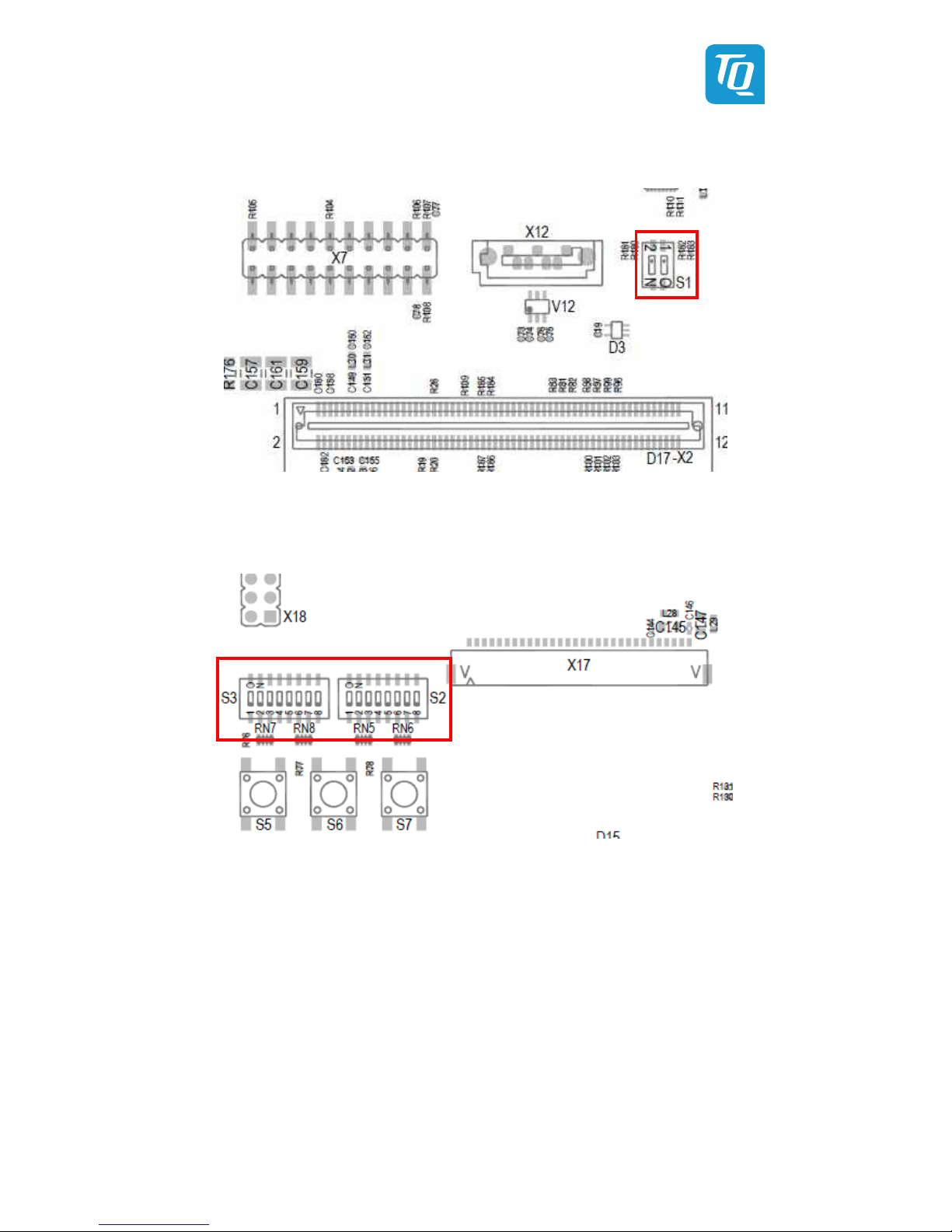
User's Manual l STK-MBa53 UM 100 l © 2013 TQ-Group Page 54
Illustration 49: Position of DIP switch S1
Illustration 50: Position of DIP switches S2, S3

User's Manual l STK-MBa53 UM 100 l © 2013 TQ-Group Page 55
4.3.6 Buzzer
Illustration 51: Block diagram buzzer
The STK-MBa53 provides a buzzer for acoustic signals. The buzzer is controlled by P2 of the IC-port expander PCA9554.
Table 75: Buzzer
Manufacturer / number Description
PUI Audio / SMI-1324-TW-5V-2-R
• Buzzer
• 5 V (typ.), 30 mA (max.)
• Resonant frequency 2,400 ±400 Hz
• SPL 88 dBA @ 100 mm (min.)
• –40 °C to +85 °C
Illustration 52: Position of buzzer

User's Manual l STK-MBa53 UM 100 l © 2013 TQ-Group Page 56
5.
5.5.
5. MECHANICS SPECIFICAT
MECHANICS SPECIFICATMECHANICS SPECIFICAT
MECHANICS SPECIFICATION
IONION
ION
5.1
5.15.1
5.1 General notes
General notesGeneral notes
General notes
• The STK-MBa53 is assembled on one side with SMD and THD components
• High pin count SMD connectors with 0.8 mm pitch
5.2
5.25.2
5.2 Dimensions
DimensionsDimensions
Dimensions
• Dimensions: 170 mm × 170 mm (each ±0.2 mm, see Illustration 54)
• Height: Minimum 22.4 mm
• Mounting holes: 6 holes with 4.3 mm diameter (see Illustration 54)
• Weight: Approximately 200 grams
Illustration 53: Height of STK-MBa53
Illustration 54: Dimension drawing of STK-MBa53

User's Manual l STK-MBa53 UM 100 l © 2013 TQ-Group Page 57
5.3
5.35.3
5.3 Housing
HousingHousing
Housing
The form factor and the holes of the STK-MBa53 are designed to be mounted in the COMSys housing.
For further information please contact the TQ-Support.
5.4
5.45.4
5.4 Thermal management
Thermal managementThermal management
Thermal management
No special precautions have been met concerning the thermal management of the STK-MBa53.
5.5
5.55.5
5.5 Component placement
Component placementComponent placement
Component placement
The component placement of the top side is shown in the following illustration.
No components are assembled on the bottom side.
Illustration 55: Component placement top

User's Manual l STK-MBa53 UM 100 l © 2013 TQ-Group Page 58
6.
6.6.
6. SAFETY REQUIREMENTS
SAFETY REQUIREMENTS SAFETY REQUIREMENTS
SAFETY REQUIREMENTS AND PROTECTIVE REGUL
AND PROTECTIVE REGULAND PROTECTIVE REGUL
AND PROTECTIVE REGULATIONS
ATIONSATIONS
ATIONS
6.1
6.16.1
6.1 EMC
EMCEMC
EMC
Because the STK-MBa53 is a development platform, no EMC specific tests have been carried out.
During the development of the STK-MBa53 the following standard was taken into account:
EMC-Interference radiation:
Measurement of the electrically radiated emission for standard, residential, commercial and light industrial environments in the
range of 30 MHz to 1 GHz according to DIN EN 55022 A1:2007.
6.2
6.26.2
6.2 ESD
ESDESD
ESD
Most of the interfaces on the STK-MBa53 are protected against electrostatic discharge13.
The interfaces, which provide an ESD protection is described in the corresponding paragraphs in section 4.
Following measures are recommended for a baseboard:
• Generally applicable: Shielding of the inputs
(shielding connected well to ground / housing on both ends)
• Supply voltages: Protection by suppressor diode(s)
• Slow signal lines: RC filtering, perhaps Zener diode(s)
• Fast signal lines: Integrated protective devices (suppressor diode arrays)
6.3
6.36.3
6.3 Operational safety and personal security
Operational safety and personal securityOperational safety and personal security
Operational safety and personal security
Due to the occurring voltages (≤30 V DC), tests with respect to the operational and personal safety have not been carried out.
6.4
6.46.4
6.4 Climatic and operational conditions
Climatic and operational conditionsClimatic and operational conditions
Climatic and operational conditions
In general reliable operation is given when the following conditions are met:
Table 76: Climatic and operational conditions
Parameter Range Remark
Permitted environmental temperature 0 °C to +70 °C Without Lithium battery CR2032
Permitted environmental temperature 0 °C to +60 °C With Lithium battery CR2032
Permitted storage temperature –10 °C to +60 °C
Relative air humidity (operation / storing) 10 % to 90 % Not condensing
6.5
6.56.5
6.5 Protection against external effects
Protection against external effectsProtection against external effects
Protection against external effects
Protection class IP00 was defined for the STK-MBa53. There is no protection against foreign objects, touch or humidity.
6.6
6.66.6
6.6 Reliability and service life
Reliability and service lifeReliability and service life
Reliability and service life
No detailed MTBF calculation has been done for the STK-MBa53. The STK-MBa53 is designed to be insensitive to vibration and
impact. Middle grade connectors, which guarantee at least 100 mating cycles, were used for the STK-MBa53.
The connector for the LVDS interface guarantees 30 mating cycles.
Information to the mating cycles of the remaining connectors can be looked up in the corresponding paragraphs in section 4.
6.7
6.76.7
6.7 Environment protection
Environment protectionEnvironment protection
Environment protection
6.7.1 RoHS compliance
The STK-MBa53 is manufactured RoHS compliant.
• All used components and assemblies are RoHS compliant
• RoHS compliant soldering processes are used
6.7.2 WEEE regulation
The company placing the product on the market is responsible for the observance of the WEEE regulation.
To be able to reuse the product, it is produced in such a way (a modular construction) that it can be easily repaired and
disassembled.
13
They JTAG interface is protected against ESD.

User's Manual l STK-MBa53 UM 100 l © 2013 TQ-Group Page 59
6.7.3 Batteries
6.7.3.1 General notes
Due to technical reasons a battery is necessary for this product. Batteries containing mercury (Hg), cadmium (Cd) or lead (Pb) are
not used. To allow a separate disposal, batteries are generally only mounted in sockets.
6.7.3.2 Lithium batteries
The requirements concerning special provision 188 of the ADR (section 3.3) are complied with for Lithium batteries.
There is therefore no classification as dangerous goods:
• Basic lithium content per cell not more than 1 g
(except for lithium ion and lithium polymer cells for which a lithium content of not more than
1.5 g per cell applies (equals 5 Ah)).
• Basic lithium content per battery not more than 2 g
(except for lithium ion batteries for which a lithium content of not more than 8 g per cell applies (equals 26 Ah)).
• Lithium cells and batteries are examined according to UN document ST/SG/AC.10-1.
• During transport a short circuit or discharging of the socketed lithium battery is prevented by extricable insulating
foils or by other suitable insulating measures.
6.8
6.86.8
6.8 Other entries
Other entriesOther entries
Other entries
By environmentally friendly processes, production equipment and products, we contribute to the protection of our
environment.
The energy consumption of this subassembly is minimised by suitable measures.
Printed pc-boards are delivered in reusable packaging. Modules and devices are delivered in an outer packaging of paper,
cardboard or other recyclable material.
Due to the fact that at the moment there is still no technical equivalent alternative for printed circuit boards with bromine-
containing flame protection (FR4 material), such printed circuit boards are still used.
No use of PCB containing capacitors and transformers (polychlorinated biphenyls).
These points are an essential part of the following laws:
• The law to encourage the circular flow economy and assurance of the environmentally
acceptable removal of waste as at 27.9.94
(source of information: BGBl I 1994, 2705)
• Regulation with respect to the utilization and proof of removal as at 1.9.96
(source of information: BGBl I 1996, 1382, (1997, 2860)
• Regulation with respect to the avoidance and utilization of packaging waste as at 21.8.98
(source of information: BGBl I 1998, 2379)
• Regulation with respect to the European Waste Directory as at 1.12.01
(source of information: BGBl I 2001, 3379)
This information is to be seen as notes. Tests or certifications were not carried out in this respect.
7.
7.7.
7. SOFTWARE
SOFTWARESOFTWARE
SOFTWARE
No software is required for the STK-MBa53. More information can be found in the Support Wiki for the TQMa53.

User's Manual l STK-MBa53 UM 100 l © 2013 TQ-Group Page 60
8.
8.8.
8. APPENDIX
APPENDIXAPPENDIX
APPENDIX
8.1
8.18.1
8.1 References
ReferencesReferences
References
Table 77: Further applicable documents
No. Name Date Company
(1) TQMa53 User’s Manual Rev. 0200, 03/2013 TQ-Systems GmbH
(2) i.MX53 Multimedia Applications Processor Reference Manual Rev. 2.1, 06/2012 Freescale
(3) Serial ATA Specification Rev 1.0a, Jan. 2003 APT Technologies
(4) USB 2.0 Specification Revision 2.0 Intel
(5) Data sheet Belfuse SSQ 1.5 SSQD1005 Bel Fuse
(6) Data sheet SGTL5000 Rev . 4.0 / Nov. 2011 Freescale
(7) Data sheet LM75A Rev. 04 / July 2007 NXP
(8) Data sheet TFP410 May 2011 TI

TQ
TQTQ
TQ----Systems G mbH
Syst ems Gmb HSyste ms GmbH
Syst ems Gmb H
Mühlstraße 2 l Gut Delling l 82229 Seefeld
info@tq-group.com l www.tq-group.com
 Loading...