

Toyota CN-TS0171LA, CN-TS0170LA Service Manual
Specifications*
CN-TS0170LA
CN-TS0171LA
DISPLAY UNIT
PART No. (CN-TS0170LA) : 86110-0D021-B1
(CN-TS0171LA) : 86110-0D021-H0
VEHICLE : YARIS
DESTINATION : Europe
PRODUCED AFTER : Dec., 2000
General
Power Supply DC 12V (11V - 16V),
Test Voltage 13.2V
Negative Ground
Current Consumption Less than 0.5A
Display Block
Display Type Positive Pattern LCD Display
Dot-Matrix
Display Size 68×33mm
Escutcheon Color
CX-TS0170K Shadow Gray
CX-TS0171K Turquoise
Display Illumination Back-Light Type
Dimensions**(W×H×D) 180.8×68.1×133.0mm
Weight** 580g
* Specifications and the design are subject to possible modification
without notice due to improvements.
** Dimensions and Weight shown are approximate.
CN-TS0170LA / CN-TS0171LA
CONTENTS
Page Page
1 FEATUERS 2
2 SYSTEM BLOCK DIAGRAM
3 FRONT VIEW AND FUNCTIONS
4 REAR VIEW AND CONNECTORS
5 WIRING CONNECTION
6 BLOCK DIAGRAM
7 TERMINALS DESCRIPTION
2
8 IC BLOCK DIAGRAM
9 REPLACEMENT PARTS LIST
2
3
10 EXPLODED VIEW
11 WIRING DIAGRAM
3
4
12 SCHEMATIC DIAGRAM
1 FEATUERS
•
• Employing HIT 64 for the transmission with NAVI (provided only for High- grade display).
• •
•
• Featuring the function of displaying various Trip Information [Outside air temperature, Cruising Range(CN-TS0170K)
• •
instantaneous fule consumption, average fule consumption and average travelling speed].
2 SYSTEM BLOCK DIAGRAM
5
6
7
10
11
15
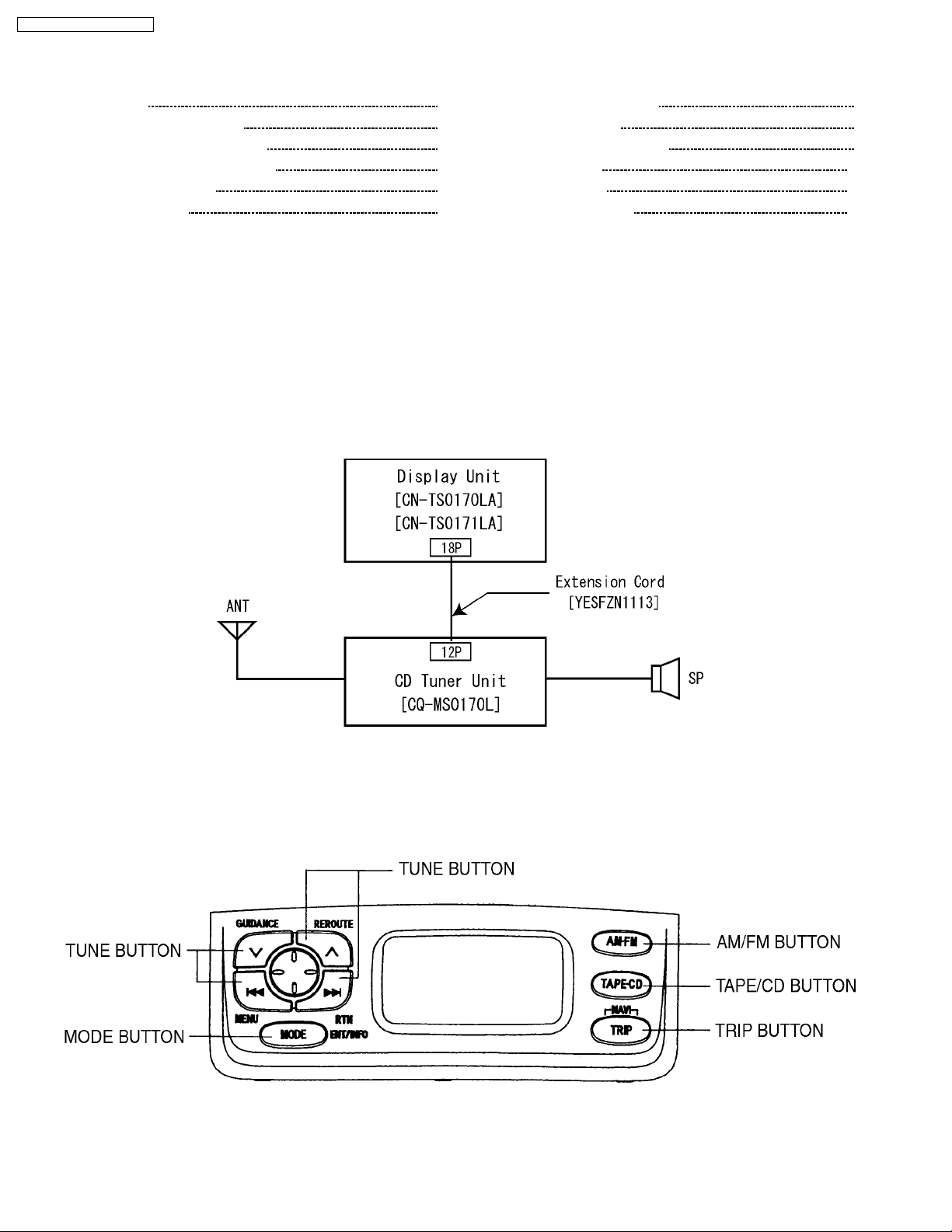
3 FRONT VIEW AND FUNCTIONS
2
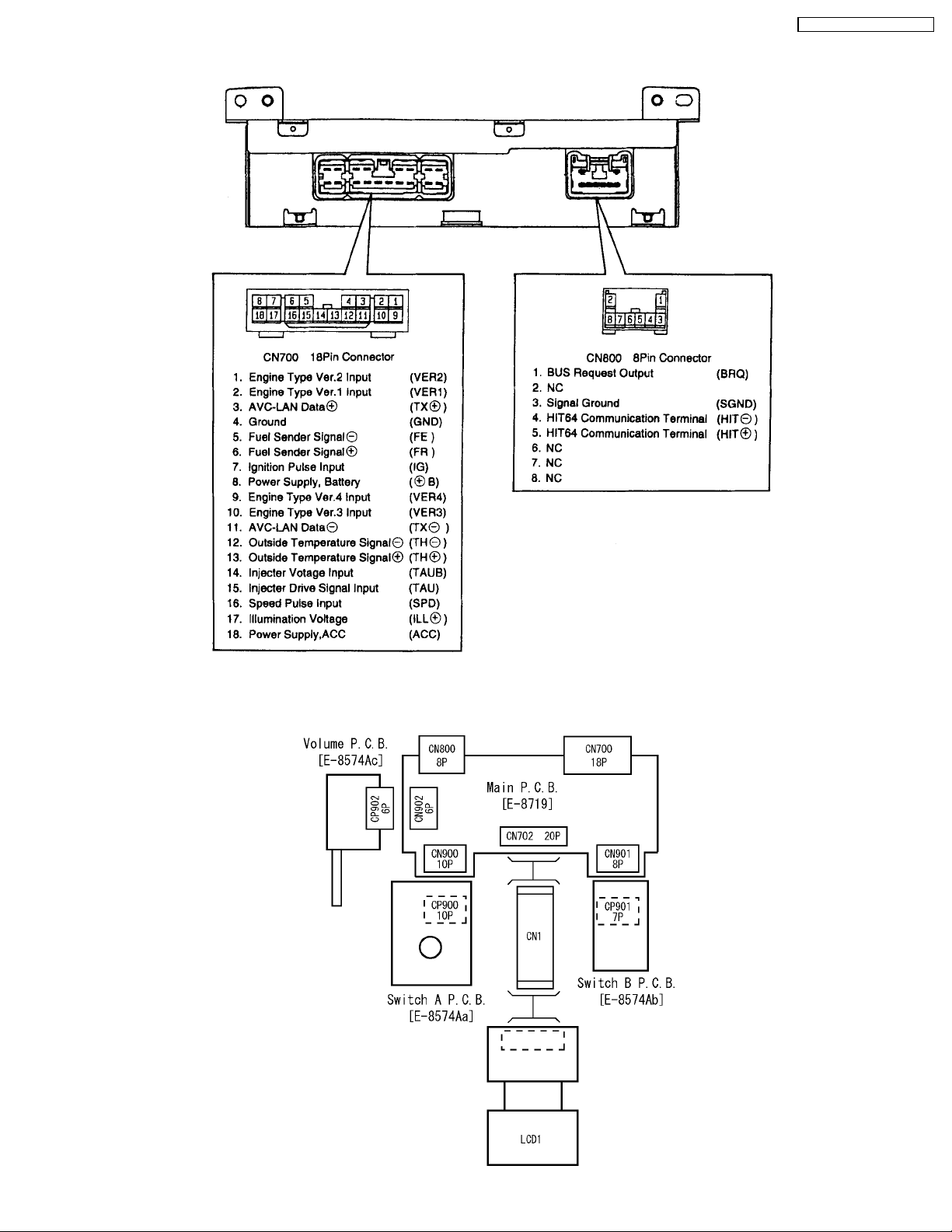
4 REAR VIEW AND CONNECTORS
CN-TS0170LA / CN-TS0171LA
5 WIRING CONNECTION
3
CN-TS0170LA / CN-TS0171LA
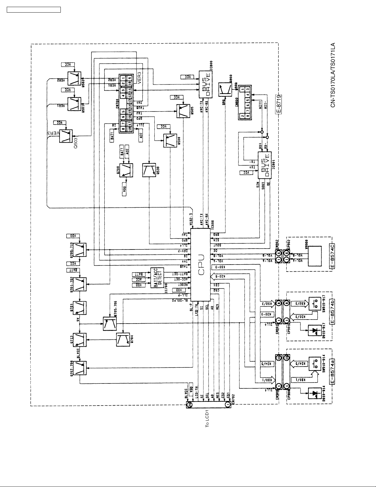
6 BLOCK DIAGRAM
4
7 TERMINALS DESCRIPTION
CN-TS0170LA / CN-TS0171LA
7.1. Main/Display Block
IC600 : C2CBHG000070
Pin
No.
1 D/A1 (NC) - - 2 D/A0 (NC) - - 3 NC - - 4 NC - - 5 TAU Injecter Pulse Input I 0
6 GND GND - 0
7 CNVSS GND - 0
8 XCIN Crystal Oscillator Input
9 XCOUT Crystal Oscillator Output
10 RESET Reset Input I 5.1
11 XOUT Crystal Oscillator Output
12 VSS GND - 0
13 XIN Crystal Oscillator Input
14 VCC +5V Power Supply - 5.1
15 BYTE +5V Power Supply - 5.1
16 +B DET Power Supply Level
17 ACC DET Power Supply Level
18 SPD Speed Pulse Input I 0
19 AVC TM AVC-LAN Start/Stop Detection I 0
20 DRV P Internal Power Supply Control O 5.1
21 NC - - 22 NC - - 23 VOL B Volume Pulse Counter Input I 0.5
24 VOL A Volume Pulse Counter Input I 0.5
25 DE Enab;e Signal Output for HIT64 O 0
26 HBRQ Bus Request Signal Output for
27 AVC RX AVC-LAN Data Input I 0
28 AVC TX AVC-LAN Data Output O 0
29 SI Serial Data Output for LCD
30 NC - - 31 SCL Serial Clock Output for LCD
32 CS2 Chip Select Output for LCD
33 SOUT Serial Data Output for HIT64 O 0
34 SIN Serial Data Input for HIT64 I 2.3
35 CS1 Chip Select Output for LCD
36 A0 Data/Command Selector for LCD
37 NC - - 38 NC - - 39 NC - - 40 LCD-P (NC) - - 41 THM-P (NC) - - 42 BL-P LCD Back Light Control O 5.1
43 RES Reset Output for LCD Driver O 0
44 HPM (NC) - - 45 MODE2 Back Light Dimmer Control
46 MODE1 - - 47 MODE0 Illumination Control Output O 5.1
48 CS1 (NC) - - 49 KEY S3 Key Scan Source Output 3 O 0
50 KEY S2 Key Scan Source Output 2 O 4.9
51 KEY S1 Key Scan Source Output 1 O 5
52 KEY S0 Key Scan Source Output 0 O 4.9
53 KEY D7 Key Scan Input 7 I 5.1
54 KEY D6 Key Scan Input 6 I 5.1
55 KEY D5 Key Scan Input 5 I 5.1
56 KEY D4 Key Scan Input 4 I 5.1
Port Descriptions I/O Vol.
(32.768kHz)
(32.768kHz)
(10MHz)
(10MHz)
Detection(+B)
Detection(ACC)
HIT64
Driver
Driver
Driver
Driver
Driver
Output
I 1.5
O 1.3
O 2.5
I 2.3
I 5.1
I 5.0
O 0
O 0
O 5.1
O 5.1
O 4.9
O 0
O 5.1
(V)
Pin
No.
57 KEY D3 Key Scan Input 3 I 5.1
59 KEY D2 Key Scan Input 2 I 5.1
59 KEY D1 Key Scan Input 1 I 5.1
60 VCC +5V Power Supply - 5.1
61 KEY D0 Key Scan Input 0 I 5.1
62 VSS GND - 0
63 MODEL3 Model Selector Signal 3 I 5.1
64 MODEL2 Model Selector Signal 2 I 5.1
65 MODEL1 Model Selector Signal 1 I 5.1
66 MODEL0 Model Selector Signal 0 I 5.1
67 VER4 Engine Type Signal 4 I 0
68 VER3 Engine Type Signal 3 I 0
69 VER2 Engine Type Signal 2 I 0
70 VER1 Engine Type Signal 1 I 0
71 VREF-D9
72 VREF-D8
73 VREF-D7
74 VREF-D6
75 VREF-D5 Reset Detection for LCD Driver I 5.1
76 TEST MODE
77 VREF-D3
78 VREF-D2
79-86 DM-D9 - D2 - - 87-89 NC - - -
90 LCD TEMP LCD Temperature Detection
91 IG Ignition Voltage Input I 0
92 FUEL Fuel Meter Detection Signal I 5.1
93 TEMP Open Air Temperature Sensor
94 AVSS GND - 0
95 TAUB Injecter Drive Voltage Input I 0
96 VREF +5V Power Supply - 5.1
97 AVCC +5V Power Supply - 5.1
98 L (NC) - - 99 NC - - -
100 ILL+ Illumination Detect I 0
Port Descriptions I/O Vol.
(NC)
(NC)
(NC)
(NC)
(NC)
(NC)
(NC)
- - -
- - -
- - -
- - -
- - -
- - -
- - -
Thermister Input
Input
I 3.2
I 0
Note :
Voltage measuerments are with respect to ground, with a
voltmeter (Internal resistance : 10M ohms.)
(V)
5
 Loading...