

Page 1

User’s Manual
TM-P3BX TM-P3VAP
ISA/ PCI/ AGP Mainboard
with onboard PCI IDE and super Multi-I/O.
Version: 2.0
1
Page 2

User’s Manual
Copyright
Copyright © 1998 by this manufacturer. All rights reserved. No part of this
publication may be reproduced, transmitted, transcribed, stored in a retrieval system,
or translated into any language or computer language, in any form or by any means,
electronic, mechanical, magnetic, optical, manual or otherwise, without the prior
written consent of this manufacturer.
Disclaimer
This manufacturer makes no representations or warranties, either expressed or
implied, with respect to the contents hereof and specifically disclaims any
warranties, merchantability or fitness for any particular purpose. Any software
described in this manual is sold or licensed “as is”. Should the programs prove
defective following their purchase, the buyer (and not this manufacturer, its
distributor, or its dealor) assumes the entire cost of all necessary servicing, repair,
and any incidental or consequential damages resulting from any defect in the
software. Further these manufacturer reserves the right to revise this publication and
to make changes from time to time in the contents hereof without obligation to
notify any person of such revision or changes.
Trademark Acknowledgement
Intel and Pentium are registered trademarks of Intel Corporation. Award is a
registered trademark of Award Software Inc. Other brand and product names are
trademarks and/or registered trademarks of their respective holders.
Printed in Taiwan
2
Page 3

User’s Manual
Overview
The TM-P3BX\VA are a Pentium II\III based mainboard that utilizes Intel
82440BX and VIA chipset on ATX PCI/ ISA platform. This mainboard is
designed for Pentium II\III CPU, and supports new architectures such as high
speed AGP graphic port, Ultra DMA/33/66, Bus Master IDE, SDRAM
memory and expandable to a maximum 1GMB. There is no second level
cache onboard since the cache is on the Pentium II\III CPU card.
In addition to above features, TM-P3BX\VA implements most advanced
technology such as Synchronous switching regulator, CPU thermal
protection, CPU fan monitoring, System voltage monitoring, Over
current protection, Modem Wake Up, Keyboard power on, PS/2 mouse
power on, Debug sensor on board and user-friendly Jumper-less.
The most unique feature of the TM-P3BX\VA is its capability to LED and
Voice debug onboard. When the CPU, DRAM, FDD, or VGA cards have not
been properly installed, a DIY user can isolate problems through reading the
Debug Sensor LED and instructions in the manual or hearing the voice
Dedug. To professional system test engineers or maintenance engineers, the
Debug Sensor can work as an 80 Port Debug Card. In other words, they can
use this debug sensor function to do testing and maintenance in lieu of the
80 Port Debug card.
3
Page 4

User’s Manual
Main Features
1. Debug sensor on board.
2. Support the newest specifications of ACPI.
3. Support Ultra DMA/33/ 66 (VIA)-highest rate IDE (must be applied with
driver).
4. Support current CPUs and future higher speed CPUs that are
compatible with SECC Socket.
5. Support IR/Consumer IR/USB and PS/2 device.
6. Support modem ring on.
7. Compatible with PCI 2.1 Spec.
8. With the “power saving” feature, the CPU cooler automatically stops
when the system enters the green mode state.
9. CPU cooler connector built in.
10. Supports Intel LDCM Network Manageability.
11. Supports ECC or Non-ECC type DRAM module.
12. Support Keyboard Power On.
13. Support PS/2 Mouse Power On.
14. Supports BIOS in setting CPU type.
15. Supports automatic closing of the unused DIMM/ PCI clock to
reduce noise.
4
Page 5

User’s Manual
CONTENTS
COPYRIGHT...............................................................................2
DISCLAIMER..............................................................................2
OVERVIEW.................................................................................3
MAIN FEATURES.......................................................................4
CONTENTS................................................................................5
INTRODUCTION.........................................................................8
A.SPECIFICATIONS....................................................................7
SETUP GUIDE............................................................................9
A.LAYOUT DIAGRAM..................................................................9
B.SMART DEBUG ON BORAD & S1 SET UP…………….
…………..9
C.CPU VOLTAGE AND
FREQUENCIES…………………………….10
D.EDO/ SDRAM INSTALLATION PROCEDURES:......................13
E.OTHER JUMPER SETTINGS...................................................15
F.NOTE TO BIOS UPDATE.......................................................17
G.KEYBOARD/ PS/2 MOUSE POWER ON AND MODEM RING ON
18
H.SYSTEM HEALTH MONITOR.................................................. 20
I. EDO/ SDRAM CONFIGURATIONTABLE:...............................22
AWARD BIOS SETUP.............................................................24
A.GETTING HELP.................................................................... 24
5
Page 6

User’s Manual
B.THE MAIN MENU..................................................................25
1.Standard CMOS Setup....................................................26
2.BIOS Features Setup.......................................................27
3.Chipset Features Setup...................................................31
4.Power Management.........................................................35
5.PNP/PCI Configuration Setup.........................................37
6.Load BIOS Default...........................................................39
7.Load Setup Default..........................................................39
8.Integrated Peripherals Setup...........................................39
9.Password Setting.............................................................42
10.IDE HDD Auto Detection...............................................43
11.Hard Disk Low Level Format Utility...............................43
12.Exiting the Setup Program.............................................44
TECHNICAL INFORMATION...................................................44
A.BLOCK DLAGRAM.................................................................44
B.I/O CONNECTOR MAP......................................................... 45
C.THE TRANSFER RATE OF IDE PIO AND DMA MODES............46
D.THE COMPUTER BOOT FLOW.CHART..................................47
E. FEATURES INTRODUCTION...................................................48
F.TIME AND DMA CHANNELS MAP.....................................50
G.INTERRUPT MAP............................................................50
H.RTC AND CMOS RAM MAP..............................................51
I.POST CODE........................................................................ 52
J.PROBLEM SHEET..................................................................57
UTILITY GUIDE........................................................................58
EXTERNAL 3.5" DRIVE BAY .................................................59
6
Page 7

User’s Manual
7
Page 8

User’s Manual
Introduction
A. Specifications
System Chipset Intel 82440 BX and VIA 693A+596B (or 686A in
Q1, 00) chipset.
CPU Intel Pentium II\III processors, support
233/266/300/333 (Ex. Clk 66 MHz).
300/350/400/450/500 550/600 (Ex. Clk 100MHz).
533/600 (Ex. Clk 133 MHz)
Memory Expandable to 768MB (3 banks) with three 168-
pin DIMM socket {support 3.3 V EDO (66MHz
only) / SDRAM (66MHz/ 100MHz)}.
I/O Winbond 83977, two high speed 16550
compatible serial ports, one Multi-Mode.
Parallel Port support SPP/EPP/ECP standard
mode.
Two onboard PCI IDE Ports (32-bit data transfer).
LS-120/ ZIP FDD, IrDA/ ASK IR/ Consumer IR.
Dual USB ports
Support two 360/720KB/1.2/1.44/2.88MB floppy
disk devices.
One PS/2 Mouse port.
BIOS Award System BIOS installed in socket (Flash and
PnP).
Expansion slots One AGP slot, five PCI Master Slots and two 16-
bit ISA Slots.
Voltage Auto 1.5V-3.5V
Dimension 4-layer PCB, size (300mm x 190mm).
Others Support BIOS setting CPU type (Jumper-less),
CPU Auto Temperature Sensor & Music Alarm,
voltage monitor and CPU Fan monitor, Bus
Master/ Ultra DMA/33, ACPI, AGP Bus, Keyboard
Power On, PS/2 Mouse Power On, Modem Ring
On, LAN wake up, Voice & Debug sensor on
board.
8
Page 9
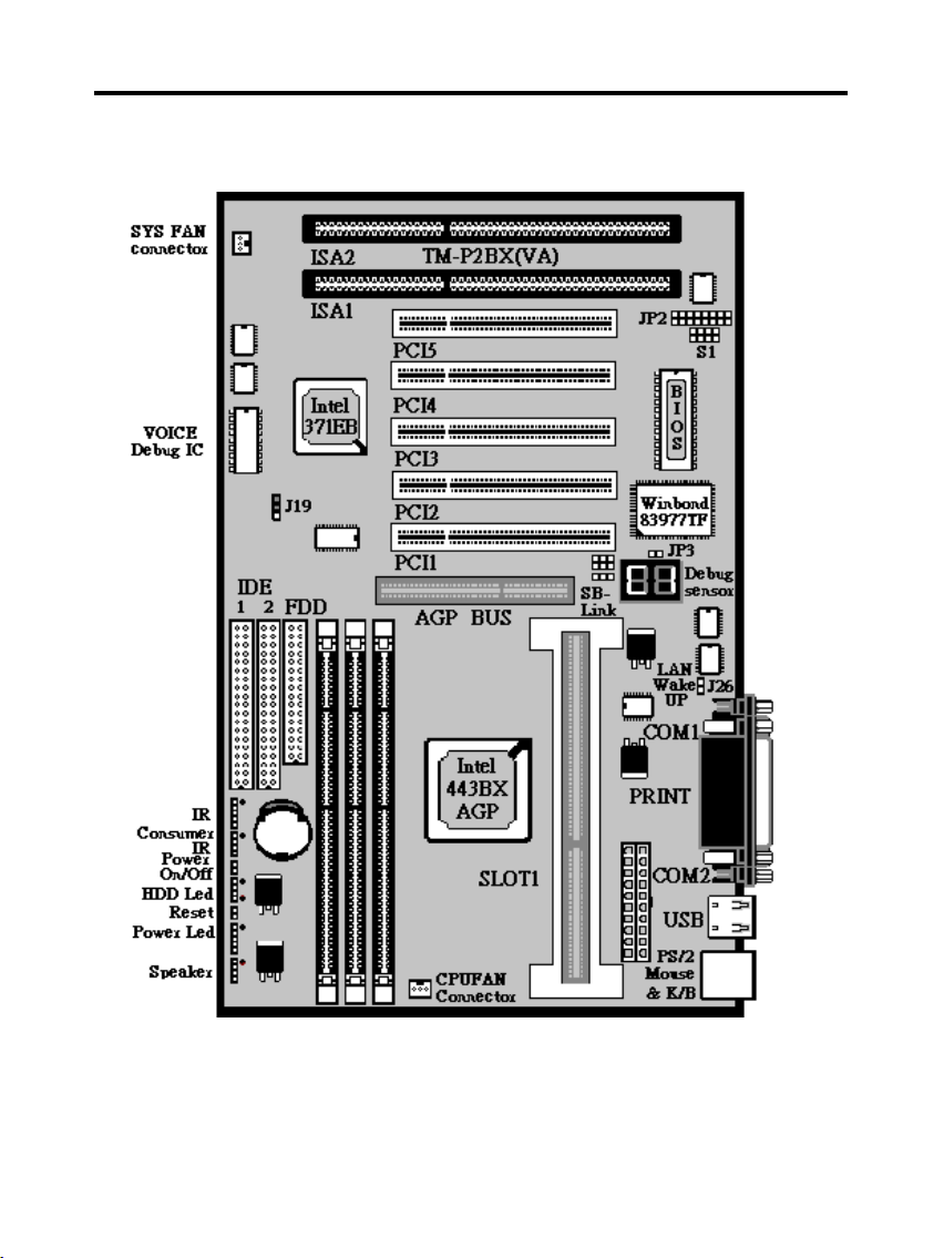
User’s Manual
Setup Guide
A. Layout Diagram
JP2 : Ex.Debug display connector.
Jp3 : Short=On board debug display
Open=Ex.Debug display
9
Page 10

User’s Manual
B. Voice / LED Debug On Board & S1 set up
When the CPU, DRAM, Cache RAM, FDD or VGA card have not been properly
installed, user can isolate those basic problems through the Debug Sensor LED and
instructions from the manual.
Error Message LED Error code Voice Debug
DRAM defect or improper connection
C1\C6
Please check memory.
CPU defect or improper connection
FF
Please check CPU.
Display card defect or improper
connection
OD
Please check display card
or memory.
Cache RAM Defect
61
Please check Cache RAM
Keyboard defect
05
Please check keyboard.
Floppy defect or improper connection
4E
Please check Floppy Disk
Drive connector or BIOS.
When CPU temperature over the set
point.
Your CPU temperature is too high.
When Mainboard was seriously
demaged in some of components.
Refer to page 52-56
for other Error Codes.
The Mainboard components may be
demaged, please sent it bck to your
supplier for repairing.
S1 Set up
In case the CPU you use is belonged old style - Multiplier type, you may refer
to following set up. All the new frequency-fixed CPU are Auto-Detect so that
don’t need to set up S1.
S1
Pin 1 Pin 2 Pin 3 Pin 4 Multiplier
Off Off Off Off X2
On On On Off X2.5
On On Off On X3
On On Off Off X 3.5
On Off On On X 4
On Off On Off X 4.5
On Off Off On X 5
On Off Off Off X 5.5
10
Page 11
User’s Manual
ROM PCI/ISA BIOS (2A69KTJ9)
CHIPSET FEATURE SETUP
AWARD SOFTWARE, INC
Auto Configuration : Enabled Auto Detect DIMM/ PCI
Clk
: Enabled
EDO DRAM Speed Selection : 60ns
EDO CASx# MA Wait State : 2
EDO RASx# Wait State : 2
SDRAM RAS-to CAS Delay : 3 Spread Spectrum : Disabled
SDRAM RAS Precharge
Time
: 3 CPU Warning Temperature : Disabled
SDRAM CAS latency Time : Auto Current CPU Temperature : 28℃/ 82℉
DRAM Data Integrity Mode : Non-ECC Current SYSFAN Speed :4285 RPM
System BIOS Cacheable : Enabled Current CPUFAN Speed :4000 RPM
Video BIOS Cacheable : Enabled Current Vin3 (V) : 2.88V
Video RAM Cacheable : Disabled
8 Bit I/O Recovery Time : 1
16 Bit I/O Recovery Time : 1
Memory Hole At 15M-16M : Disabled
Passive Release : Enabled
Esc : Quit Selection : Item
Delayed Transaction : Disabled F1 : Help PU/PD/+/- :
Modify
AGP Aperture Size (MB) : 64 F5 : Old Values (Shift) F2 : Color
F6 : Load BIOS Default
F7 : Load Setup Default
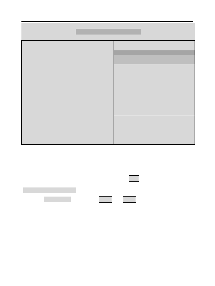
Dear Customers:
Thank you for your patronage of our products. The board you bought is a
jumper-less mainboard. The ratio and frequency of the CPU shall be set in
BIOS and the working voltage for the CPU shall be automatically detected.
Please read carefully the following instructions:
1. Power on the installed system and press the "DEL" key to enter BIOS
Setup. Select
"Chipset Features Setup" and press <Enter>.
2. Select "CPU Speed" and press "PgUp" or "PgDn" to set the CPU ratio and
frequency. The available options are Intel PII
233MHz (66X3.5), 266MHz (66X4), 300MHz (66X4.5), 333MHz (66X5),
366MHz (66X5.5), 400MHz(66X6), 433MHz(66X6.5), 466MHz(66X7),
500MHz(66X7.5).
250MHz(100X2.5), 300MHz(100X3), 350MHz(100X3.5), 400MHz(100X4),
450MHz(100X4.5), 500MHz(100X5), 550MHz(100X5.5), 600MHz(100X6)
and "Manual".
To set the CPU manually, please note the following:
11
Page 12
User’s Manual
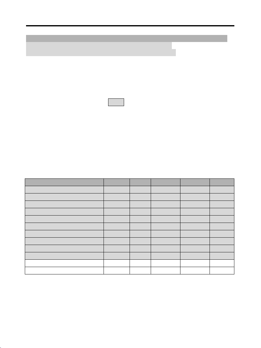
CPU Speed: "Manual" (you can manually set the CPU ratio and frequency)
CPU Ratios: x3.5, x4, x4.5, x5, x5.5, x6, x6.5, x7, x7.5
CPU Frequency: 66, 68, 75, 83, 100, 103, 112, 133Mhz
Several options are provided for the CPU external clock. You are
recommended to restore to the default setting in case of instability when the
external clock exceeds 66MHz.
NOTE: System failure may occur if the CPU frequency is set incorrectly. To
solve this problem. Press the "Insert" key on the keyboard to clear the
previously set frequency (i. c., restore the default frequency), and then reboot
the system.
Switch voltage is applied, making the temperature lower and voltage steadier.
You don’t need to adjust Voltage in Pentium II mainboard. It will
automatically send out one VID (Voltage Identification) to the mainboard
power supply to ask for the voltage it needs.
The CPU type default setting is Intel Pentium II 250MHz=100 MHz*2.5.
Intel Pentium II\III CPU family
CPU Ext. clk Ratio L1 cache L2 cache Voltage
Intel Pentium III – 600MHz 133MHz X4.5 32KB 512KB 2.8V
Intel Pentium III – 533MHz 133MHz X4 32KB 512KB 2.8V
Intel Pentium III – 600MHz 100MHz X6 32KB 512KB 2.8V
Intel Pentium III – 550MHz 100MHz X5.5 32KB 512KB 2.8V
Intel Pentium III – 500MHz 100MHz X5 32KB 512KB 2.8V
Intel Pentium III – 450MHz 100MHz X4.5 32KB 512KB 2.8V
Intel Pentium II – 450MHz 100MHz X4.5 32KB 512KB 2.8V
Intel Pentium II – 400MHz 100MHz X4 32KB 512KB 2.8V
Intel Pentium II – 350MHz 100MHz X3.5 32KB 512KB 2.8V
Intel Pentium II – 300MHz 100MHz X3 32KB 512KB 2.8V
Intel Pentium II – 333MHz 66MHz X5 32KB 512KB 2.8V
Intel Pentium II – 300MHz 66MHz X4.5 32KB 512KB 2.8V
12
Page 13
User’s Manual
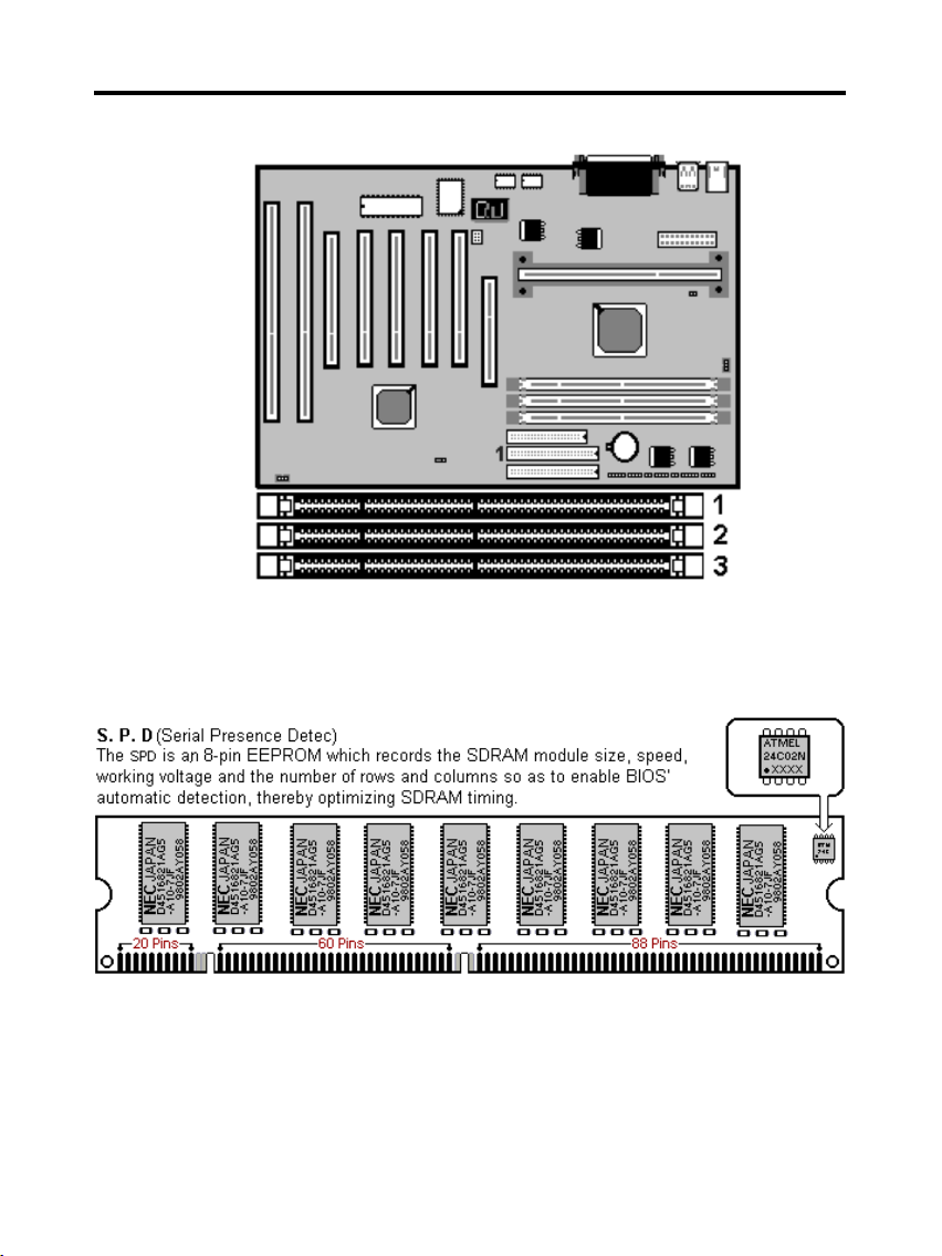
C. EDO/ SDRAM Installation Procedures:
A 168-pin DIMM can support up to 768MB 3.3V EDO (66MHz) / SDRAM
(66MHz/ 100MHz).
You are recommended to use SDRAMs. With SPD that are compliant
with PC-100. This will enable BIOS to detect the SDRAM speed, thereby
fully bring into play the efficiency of the SDRAM.
To avoid compatibility and reliability problems, you are recommended to
test the 168-pin SDRAMs before buying them since the PCB
specifications differ.
13
Page 14
User’s Manual
The following table shows the memories that have passed the PC-100
specifications.
Brand Memory size Number
TOSHIBA 8M X 08=64MB TC59S6408BFT-80
TOSHIBA 4M X 16=64MB TC59S6416BFT-80
HITACHI 8M X 08=64MB HM5264805TT-B60
HITACHI 4M X 16=64MB HM5264165TT-B60
MITSUBISHI 8M X 08=64MB M5M4V64S30ATP-8
MITSUBISHI 4M X 16=64MB M5M4V64S40ATP-8
MITSUBISHI 2M X 08=16MB M5M4V16S30DTP-8
FUJITSU 8M X 08=64MB 81F64842B-103FN
FUJITSU 4M X 16=64MB 81F641642B-103FN
TI 8M X 08=64MB TMX664814A81A7ET
TI 2M X 08=16MB TMX626812BDGE5M
SAMSUNG 8M X 08=64MB KM48S8030BT-GH
SAMSUNG 4M X 16=64MB KM416S4030BT-G10
SAMSUNG 2M X 08=16MB KM48S2020CT-GL
HYUNDAI 8M X 08=64MB HY57V658020ALTC-10P
HYUNDAI 2M X 08=16MB HY57V168010C TC-10S
LG 8M X 08=64MB GM72V66841CT7J
LG 4M X 16=64MB GM72V661641CT-7J
First, verify the working voltage of the EDO/ SDRAM module in either
DIMM socket.
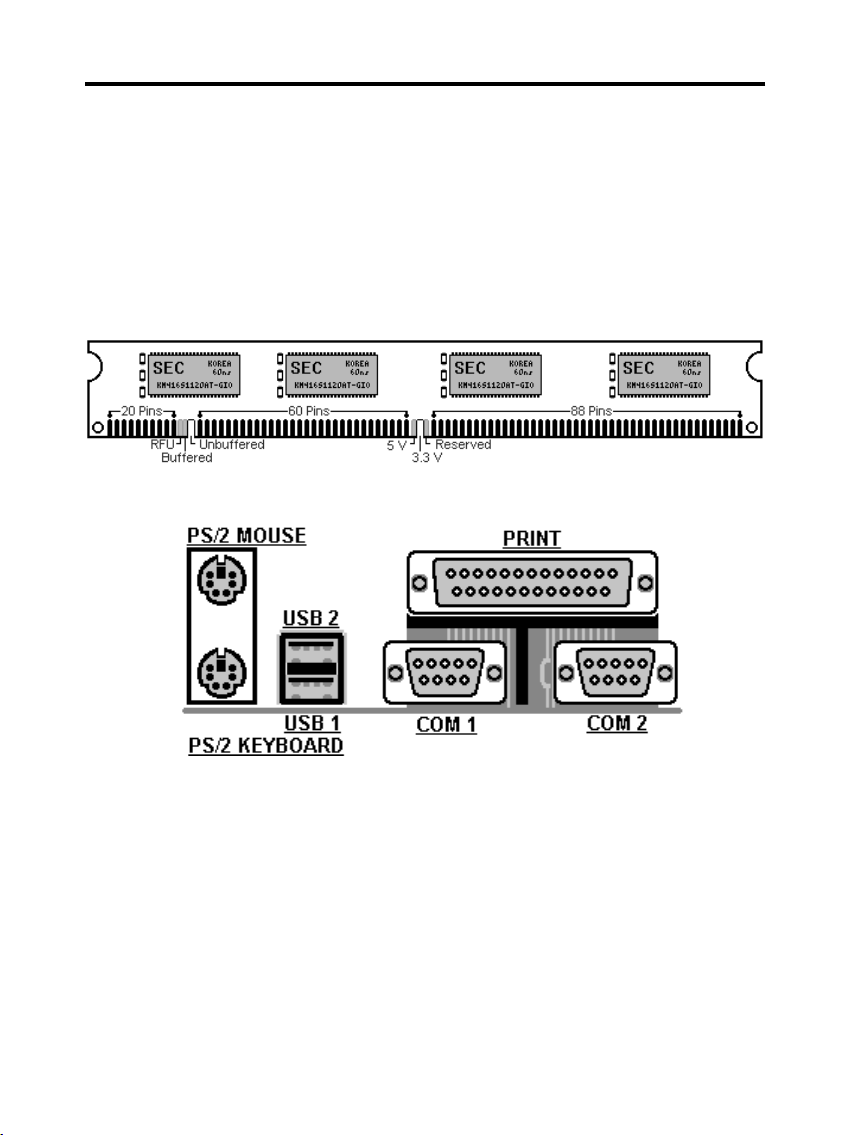
P3BX only supports 3.3V EDO/ SDRAM module. The following
illustration shows you the difference between 3.3V and 5V to ensure
your correct selection of 3.3V DIMM module for using.
You can set up the BIOS “Chipset Feature Setup” to the best working
condition basing on the type of EDO/ SDRAM you are using.
The BIOS DRAM default setting is 60 ns. Change the BIOS “Chipset
Feature Setup” default setting to 50ns for better performance, if the
chipset is marked 50ns.
Change nothing if EDO RAM is used. BIOS automatically detect the
RAM type.
MEMO for Installing System:
14
Page 15
User’s Manual
⊕ Concerning memory setup, you can find how to from “Chipset
Feature Setup” under BIOS setup. However, to avoid system unstable
or system hang, user without engineering background is not suggested
to change BIOS set up.
⊕ If system boot failure, please clean DIMM socket (with clean oil) or
polish Gold-Finger of DRAM with soft eraser, and try again.
The Dual Inline Memory Module (DIMM) must be 3.3 Volt and
Unbuffered Synchronus DRAM (SDRAM) 8MB, 16MB, 32MB, 64MB,
128MB or 256MB. The following illustration shows the type of DIMM
Module.
168-PIN SDRAM DIMM Notch Key Definitions
15
Page 16
User’s Manual
D. Other Jumper Settings
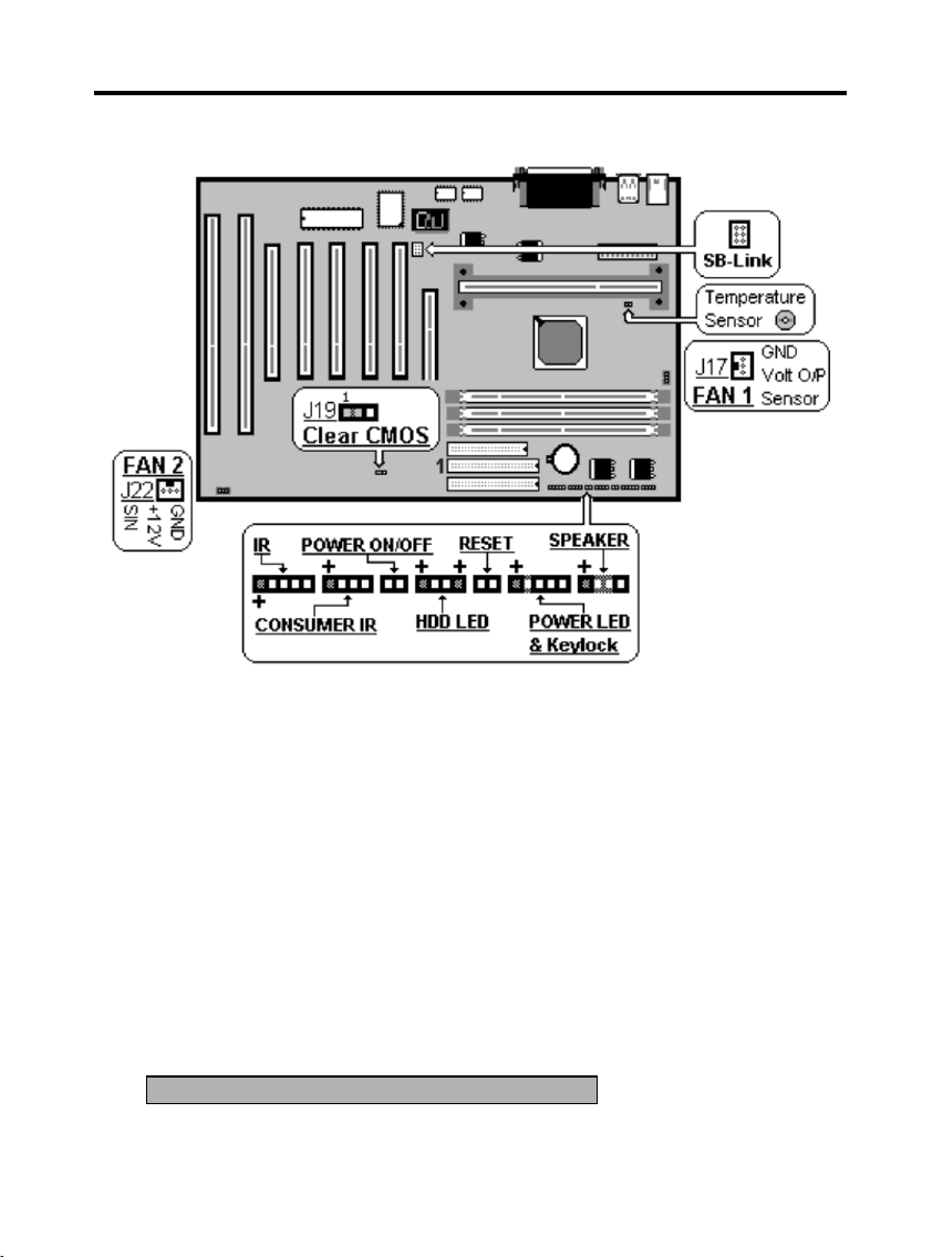
Speaker: Connect to the system’s speaker for beeping.
Keylock: Keyboard lock switch and Power LED connector.
Reset: Short to restart system.
HDD LED: LED ON when on board PCI IDE hard disk activates.
POWER SW (FOR ATX POWER SUPPLY):
The button should be a momentary switch that is normally open.
Pushing the ATX Power Switch will immediately change the system
status. Before or during “POST”, you need to hold the button for four
seconds in order to turn off the system.
J19: Clear CMOS
Turn off the system and short pins 2-3 to clear CMOS. Then short pins
1-2 before turning it on.
J19
16
Page 17

User’s Manual
1-2 Normal operation(Default).
2-3 for clearing CMOS Data.
CPU Cooler Fan connector
This is the connector for CPU cooler. Never use the jumper to short the
connector. Serious damages caused this way will not be warrantied.
Creative SB-Link
It is used to connect the AWE64 or other compatible sound cards so
that they are made compatible with the ISA-compatible SB16 sound
cards.
E. Note to BIOS Update
Do not update the BIOS if no abnormalities occur. However, if BIOS
update is needed, consult your dealer first. Prior to updating your BIOS,
you are recommended to save the original BIOS values.
1. Download the AWARD BIOS Flash Utility file (Awdflash.exe)
2. Download the BIOS file used by your mainboard(e.g., BXV110N.BIN)
3. Reboot your system (but do not run Himem.sys and Emm386.exe)
to
execute the new BIOS program.
4. Execute these commands: Awdflash BXV110N.BIN
5. When this message displays: "Do you want to save BIOS (Y/N)?"
Type "N"
6. When this message displays: "Are you sure to program (Y/N)?"
Type "Y"
7. Turn off power to your system to clear the CMOS data.
8. Turn on the power to test if your system is running normal.
17
Page 18
User’s Manual
F. Keyboard/ PS/2 Mouse Power On and MODEM Ring on
To make sure the 5VSB signal nearly to 750mA (Amperage) from
ATX Power Supply, or if your keyboard consuming power than
300mA, it's better to upgrade your ATX Power Supply to 1A for
working perfectly.
If you are going to use the function of keyboard and PS/2 mouse power on,
then, the power-switch will be becoming useless automatically (unable to be
used).
ROM PC/ISA BIOS (2A69KTJ9)
INTEGRATED PERIPHERALS
AWARD SOFTWARE, INC.
IDE HDD Block Mode : Enabled Onboard Serial Port 2 : 2F8H / IRQ3
IDE Primary Master PIO : AUTO UART Mode Select : Normal
IDE Primary Slave PIO : AUTO
IDE Secondary Master PIO : AUTO Onboard Parallel Port : 378H/IRQ 7
IDE Secondary Slave PIO : AUTO Parallel Port Mode : ECP+EPP
IDE Primary Master UDMA : AUTO ECP Mode Use DMA : 3
IDE Primary Slave UDMA : AUTO EPP Mode Select : EPP 1.9
IDE Secondary Master
UDMA
: AUTO
IDE Secondary Slave
UDMA
: AUTO
On-Chip Primary PCI IDE : Enabled
On-Chip Secondary PCI IDE : Enabled
USB Keyboard Support : Disabled
Init AGP Display First : Enabled
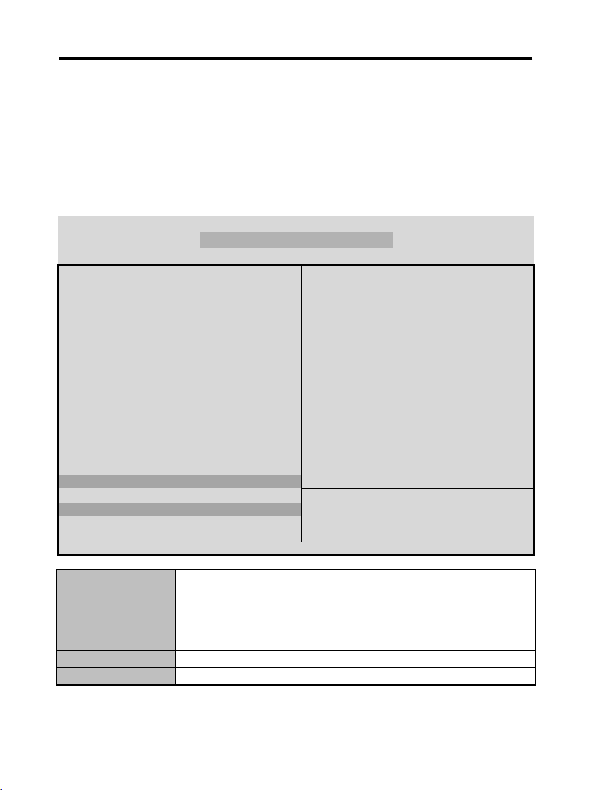
POWER ON Function : Hot KEY
Esc : Quit Selection : Item
Hot Key Power ON : Ctrl-F12 F1 : Help PU/PD/+/- : Modify
KBC input clock : 8MHz F5 : Old Values (Shift)F2 : Color
Onboard FDC Controller : Enabled F6 : Load BIOS Default
Onboard Serial Port 1 : 3F8H / IRQ4 F7 : Load Setup Default
Hot KEY When user select this option, it will show another line
lines as Hot Key Power ON: Ctrl-
F(1/2/3/4/5/6/7/8/9/10/11/12) select any you like. After
power off, if user key in the "Ctrl-F?", it will power on the
system.
PS/2 Mouse Left It will power on the system by PS/2 mouse left.
PS/2 Mouse Right It will power on the system by PS/2 mouse Right.
18
Page 19
User’s Manual
Button Only Only the power button can power on the system.
Modem Ring On Function Operation:
ROM PCI / ISA BIOS (2A69KTJ9)
POWER MANAGEMENT SETUP
AWARD SOFTWARE, INC
Power Management : Disabled ** Reload Global Timer Events **
PM Control by APM : No IRQ[3-7, 9-15], NMI : Enabled
Video Off Method : V/H
SYNC+Blank
Primary IDE 0 : Disabled
Video Off After : Standby Primary IDE 1 : Disabled
MODEM Use IRQ : 3 Secondary IDE 0 : Disabled
Doze Mode : Disabled Secondary IDE 1 : Disabled
Standby Mode : Disabled Floppy Disk : Disabled
Suspend Mode : Disabled Serial Port : Enabled
HDD Power Down : Disabled Parallel Port : Disabled
Throttle Duty Cycle : 62.5%
ZZ Active in Suspend : Disabled
VGA Active Monitor : Enabled
Soft-Off by PWR-BTTN : Instant-Off
CPUFAN Off In Suspend : Enabled
Resume by Ring : Enabled
IRQ 8 Clock Event : Disabled
Esc : Quit Selection Item
F1 : Help PU/PD/+/- : Modify
F5 : Old Values (Shift) F2 : Color
F6 : Load BIOS Default
F7 : Load Setup Default
1. Have an external MODEM connected to COM 1 or COM 2.
2. Enter BIOS setup.
3. Select Power Management Setup.
4. This number of MODEM use IRQ has to be set as same as the IRQ of
Serial Port which you are connecting in. Please set in N/A if you are
not going to use the function of MODEM ring on.
5. Resume by Ring: Enable.
6. Save BIOS setup and Reboot.
7. Booting from DOS, Windows, or Windows 95.
8. Turn off the system by:
a. ATX-Power Switch
b. Windows 95 Software Power Off
9. System Waiting for Modem Ring On
When Modem Ringing Signal Active, System will wake-up.
19
Page 20
User’s Manual
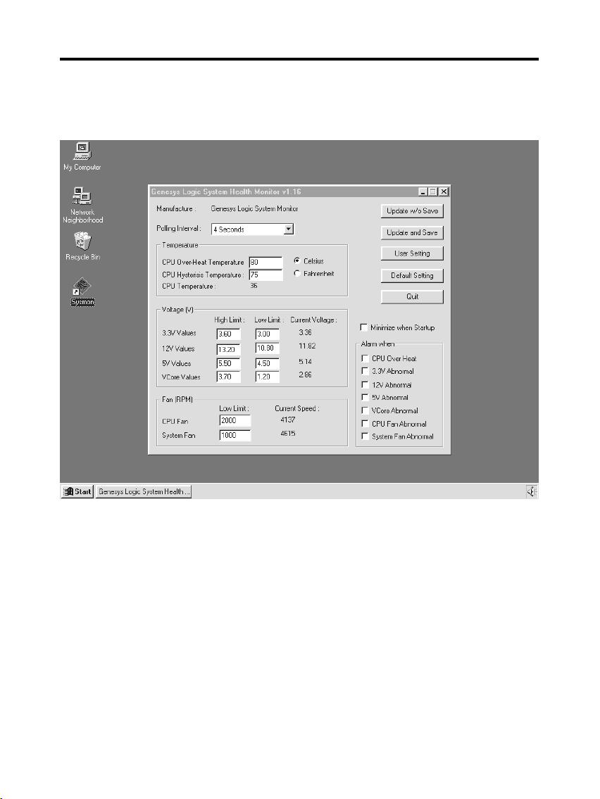
G. System Health Monitor
Fan Monitoring:
There are two fan connectors, one is for CPU, the other can be a
housing fan. When the fans speed is working abnormal, there will be
warning (Speaker Alarm) through application software such as
SM10(Small Icon for System Monitoring) to notify user. The fan
monitoring function is implemented by connecting fan to 3-pin fan
connector FAN1/ FAN2 and installing SM10. Referring to Page 19
(System Health Monitor).
20
Page 21

User’s Manual
CPU Thermal Protection:
TM-P3BX implements special thermal protection circuits. When
temperature is higher than a predefined value, there will be warning
(Speaker Alarm) through application software such as SM10 (Small Icon
for System Monitor) to notify user. It's automatically implemented by
BIOS or SMD10, no hardware installation is needed. Referring to
Page19 (System Health Monitor).
This mainboard also reserves an option to use special CPU cooling Fan.
With Thermal Sensor on it. The CPU thermal sensor should be
connected to J16.
System Voltage Monitoring:
TM-P3BX is featured with a voltage monitoring system. When you turn
on your system, this smart design will keep on monitoring your system
working voltage. If any of voltage is over the component's standard,
there will be Speaker Alarm though application software SM10 (Small
Icon For System Monitor) for a warning to user. System voltage
monitoring function monitors 5V, 12V, 3.3V and CPU voltage. It's
automatically implemented by BIOS and SM10, no hardware installation
is needed. Referring to Page 19 (System Health Monitor)
21
Page 22
User’s Manual
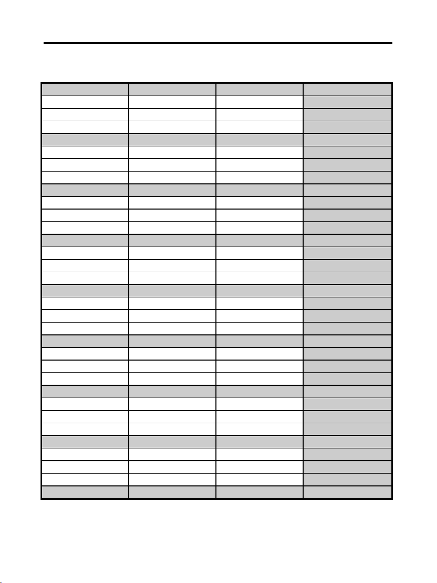
H. EDO/ SDRAM Configuration Table:
DIMM1 DIMM2 DIMM3 TOTAL
8MB 8MB --- 16MBytes
--- 8MB 8MB 16MBytes
8MB --- 8MB 16MBytes
--- 16MB --- 16MBytes
8MB 8MB 8MB 24MBytes
16MB 8MB --- 24MBytes
--- 16MB 8MB 24MBytes
16MB --- 8MB 24MBytes
16MB 16MB --- 32MBytes
--- 16MB 16MB 32MBytes
16MB --- 16MB 32MBytes
--- 32MB --- 32MBytes
16MB 16MB 8MB 40MBytes
8MB 16MB 16MB 40MBytes
32MB 8MB --- 40Mbytes
--- 32MB 8MB 40MBytes
16MB 16MB 16MB 48MBytes
32MB 8MB 8MB 48MBytes
32MB 16MB --- 48MBytes
--- 32MB 16MB 48MBytes
32MB 32MB --- 64MBytes
--- 32MB 32MB 64MBytes
--- 64MB --- 64MBytes
32MB 16MB 16MB 64MBytes
32MB 32MB 8MB 72MBytes
8MB 32MB 32MB 72MBytes
64MB 8MB --- 72Mbytes
--- 64MB 8MB 72MBytes
32MB 32MB 16MB 80MBytes
16MB 32MB 32MB 80MBytes
64MB 16MB --- 80MBytes
--- 64MB 16MB 80MBytes
22
Page 23
User’s Manual
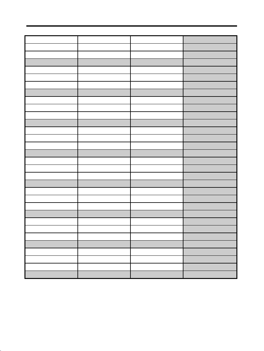
32MB 32MB 32MB 96MBytes
64MB 32MB --- 96MBytes
--- 64MB 32MB 96MBytes
16MB 64MB 16MB 96MBytes
64MB 64MB --- 128MBytes
--- 64MB 64MB 128MBytes
64MB 32MB 32MB 128MBytes
--- 128MB --- 128MBytes
64MB 64MB 8MB 136MBytes
8MB 64MB 64MB 136MBytes
128MB 8MB --- 136MBytes
--- 128MB 8MB 136MBytes
64MB 64MB 16MB 144MBytes
16MB 64MB 64MB 144MBytes
128MB 16MB --- 144Mbytes
--- 128MB 16MB 144MBytes
64MB 64MB 32MB 160MBytes
32MB 64MB 64MB 160MBytes
128MB 32MB --- 160MBytes
--- 128MB 32MB 160MBytes
64MB 64MB 64MB 192MBytes
128MB 64MB --- 192MBytes
--- 128MB 64MB 192MBytes
32MB 128MB 32MB 192MBytes
128MB 128MB --- 256MBytes
--- 128MB 128MB 256MBytes
64MB 128MB 64MB 256MBytes
--- 256MB --- 256MBytes
128MB 128MB 8MB 264MBytes
256MB --- 8MB 264MBytes
256MB 8MB --- 264MBytes
--- 256MB 8MB 264MBytes
23
Page 24
User’s Manual
128MB 128MB 32MB 288MBytes
256MB --- 32MB 288MBytes
256MB 32MB --- 288MBytes
--- 256MB 32MB 288MBytes
128MB 128MB 64MB 320MBytes
256MB --- 64MB 320MBytes
256MB 64MB --- 320MBytes
--- 256MB 64MB 320MBytes
128MB 128MB 128MB 384MBytes
256MB --- 128MB 384MBytes
256MB 128MB --- 384MBytes
--- 256MB 128MB 384MBytes
128MB 128MB 256MB 512MBytes
256MB --- 256MB 512MBytes
256MB 256MB --- 512Mbytes
--- 256MB 256MB 512MBytes
256MB 256MB 8MB 520MBytes
256MB 8MB 256MB 520MBytes
8MB 256MB 256MB 520MBytes
256MB 256MB 16MB 528MBytes
256MB 16MB 256MB 528MBytes
16MB 256MB 256MB 528MBytes
256MB 256MB 32MB 544MBytes
256MB 32MB 256MB 544MBytes
32MB 256MB 256MB 544MBytes
256MB 256MB 64MB 576MBytes
256MB 64MB 256MB 576MBytes
64MB 256MB 256MB 576MBytes
256MB 256MB 128MB 640MBytes
256MB 128MB 256MB 640MBytes
128MB 256MB 256MB 640MBytes
256MB 256MB 256MB 768MBytes
24
Page 25

AWARD BIOS Setup
Getting Help
Main Menu
The online description of the highlighted setup function is displayed at the bottom
of the screen.
Status Page Setup Menu/Option Page Setup Menu
Press F1 to pop up a small help window that describes the appropriate keys to use
and the possible selections for highlighted item. To exit the Help Window press
<Esc>.
The Main Menu
Once you enter Award BIOS CMOS Setup Utility, the Main Menu will appear on
the Screen.. Use arrow keys to select the desired items, press <Enter> to select or
enter a submenu.
ROM PC/ISA BIOS (2A6LGTJJ)
CMOS SETUP UTILITY
AWARD SOFTWARE, INC.
STANDARD CMOS SETUP
BIOS FEATURE SETUP
CHIPSET FEATURES SETUP
POWER MANAGEMENT SETUP
PNP/PCI CONFIGURATION
LOAD BIOS DEFAULTS
LOAD SETUP DEFAULTS
INTEGRATED PERIPHERALS
SUPERVISOR PASSWORD
USER PASSWORD
IDE HDD AUTO DETECTION
HDD LOW LEVEL FORMAT
SAVE & EXIT SETUP
EXIT WITHOUT SAVING
Esc : Quit : Select Item
F10 : Save & Exit Setup (Shift) F2 : Change Color
Time, Data, Hard Disk Type...
24
Page 26

AWARD BIOS Setup
1. Standard CMOS Setup
The items in Standard CMOS Setup Menu are divided into several categories. Each
category includes no, one or more than one setup items. Use the arrow keys to
highlight the item and then use the <PgUp> or <PgDn> keys to select the value you
want in each item.
ROM PCI/ISA BIOS (2A6LGTJJ)
STANDARD CMOS SETUP
AWARD SOFTWARE, INC
Date ( mm: dd: yy ) : Sat, Jul 11 1998
Time ( hh: mm: ss ) : 17 : 59 : 44
HARD DISKS TYPE SIZE CYLS HEAD PRECOMP LANDZ SECTOR MODE
--------------------------------------------------------------------------------------------------------------------------- Primary Master
: AUTO 0 0 0 0 0 0 AUTO
Primary Slave
: AUTO 0 0 0 0 0 0 AUTO
Secondary
Master
: AUTO 0 0 0 0 0 0 AUTO
Secondary Slave
: AUTO 0 0 0 0 0 0 AUTO
Driver A : 1.44M, 3.5 in.
Driver B : None Base Memory: 640K
Extended Memory: 64512K
Video : EGA/VGA Other Memory: 384K
Halt On : All, But Keyboard -----------------------------------------
Total Memory: 65536K
Esc : Quit Selection Item PU/PD/+/- : Modify
F1 : Help (Shift) F2 : Color
25
Page 27

AWARD BIOS Setup
2. BIOS Features Setup
ROM PCI/ISA BIOS (2A6LGTJJ)
BIOS FEATURE SETUP
AWARD SOFTWARE, INC
Virus Warning : Disabled Video BIOS Shadow
: Enabled
CPU Internal Cache : Enabled C8000-CBFFF Shadow
: Disabled
External Cache : Enabled CC000-CFFFF Shadow
: Disabled
Quick Power On Self Test : Enabled D0000-D3FFF Shadow
: Disabled
Boot Sequence : A, C,
SCSI
D4000-D7FFF Shadow
: Disabled
Swap Floppy Drive : Disabled D8000-DBFFF Shadow
: Disabled
Boot Up Floppy Seek : Enabled DC000-DFFFF Shadow
: Disabled
Boot Up NumLock Status : On
Boot Up System Speed : High
Gate A20 Option : Fast
Typematic Rate Setting : Disabled
Typematic Rate (Chars/Sec) : 6
Typematic Delay (Msec) : 250
Security Option : Setup
PS/2 mouse function control : Enabled
Esc : Quit Selection Item
PCI/VGA Palette Snoop : Disabled F1 : Help PU/PD/+/- : Modify
Assign IRQ For VGA
OS Select For DRAM > 64MB
Report No FDD For WIN 95
: Enabled
: Non-OS2
: No
F5 : Old Values (Shift) F2 : Color
F6 : Load BIOS Default
F7 : Load Setup Default
Virus Warning
This category flashes on the screen. During and after system boots up, any attempt
to write to the boot sector or partition table of the hard disk drive will halt the
system and the following error message will appear, in the mean time , you can run
anti-virus program to locate the problem.
!WARNING!
Disk boot sector is to be modified
Type "Y" to accept write or "N" to abort write
Award Software, Inc.
26
Page 28
AWARD BIOS Setup
Enabled: Activate automatically when the system boots up causing a warning
message to appear when anything attempts to access the boot sector
or hard disk partition table.
Disabled: No warning message to appear when anything attempt to access the
boot sector or hard disk partition table.
CPU Internal Cache/External Cache
These two categories speed up memory access. However, it depends on
CPU/chipset design. The default value is Enabled.
Enabled: Enabled cache
Disabled: Disabled cache
Quick Power On Self Test
This category speeds up Power-On-Self-Test (POST) after you power on the
computer. If it is set to Enable, BIOS will shorten or skip some check items during
POST.
Enabled: Enable quick POST
Disabled: Normal POST
Boot Sequence
This category determines which drive computer searches first for the hard disk
operation system (i.e., DOS).
A, C, SCSI / C, A, SCSI / C, CDROM, A / CDROM, C, A / D, A, SCSI / E, A,
SCSI / SCSI, A, C / SCSI, C, A / C only / LS120, C: System will first search drive
for BOOT, and then next other drive, if first driver does not boot.
Swap Floppy Drive
Users can enable this item so that the BIOS will see the hardware "Drive A:" as
"Drive B:"” , and hardware "Drive B:"” as "Drive A:"”.
Boot Up Floppy Seek
During POST, BIOS will determine if the floppy disk drive installed is 40 or 80
tracks. 360K type is 40 tracks while 720K, 1.2M and 1.44M drive types are all 80
tracks.
27
Page 29
AWARD BIOS Setup
Enabled: BIOS searches for floppy disk drive to determine if it is 40 or 80
tracks. Note that BIOS cannot tell from 720K, 1.2M or 1.44M drive
type as they are all 80 tracks.
Disabled: BIOS will not search for the type of floppy disk drive by track
number. Note that there will not be any warning message if the drive
installed is 360KB.
Boot Up NumLock Status: The default value is On.
On: Keypad is number keys
Off: Keypad is arrow keys
Boot Up System Speed
It selects the default system speed - the speed that the system will run immediately
after power up.
High: Set the speed to high
Low: Set the speed to low
Gate A20 Option
The Gate A20 Option default setting is “fast.”. This is the optimum setting for this
mainboard.
Typematic Rate Setting
This determines the typematic rate.
Enabled: Enable typematic rate
Disabled: Disable typematic rate
Typematic Rate (Chars/Sec)
6: 6 characters per second 8: 8 characters per second
10: 10 characters per second 12: 12 characters per second
15: 15 characters per second 20: 20 characters per second
24: 24 characters per second 30: 30 characters per second
28
Page 30
AWARD BIOS Setup
Typematic Delay (Msec)
It indicates the time between the first and second character displayed when you
hold a key.
250 : 250 msec 500 : 500 msec
750 : 750 msec 1000 : 1000 msec
Security Option
This category allows you to limit access to the system and Setup, or just to Setup.
System: The system will not boot and access to Setup will be denied if the
correct password is not entered at the prompt.
Setup: The system will boot, but access to Setup will be denied if the correct
password is not entered at the prompt.
NOTE: To disable security, select PASSWORD SETTING at Main Menu and then
you will be asked to enter password. Do not type anything and press <Enter> to
disable security. Once the security is disabled, the system will boot and you can
enter Setup freely.
PCI/ VGA Palette Snoop
It determines whether the MPEG ISA/ VESA VGA cards can work with PCI/ VGA
or not.
Enabled: When PCI/ VGA working with MPEG ISA/ VESA Card.
Disabled: When PCI/ VGA not working with MPEG ISA/ VESA Card.
Assign IRQ for VGA
When this items is enabled, the system will assign an IRQ for VGA. If this item is
disabled, the VGA will not occupy an IRQ; therefore the IRQ of VGA will be
released for other usage. The default value is Enabled.
OS Select for DRAM>64MB
This item allows you to access the memory that is over 64MB in OS/2.
The default value is Non-OS2.
Report No FDD For WIN95
For Windows 3.1x users set "No"; for Windows 95 users set "No" or "Yes".
The default value is no.
Video BIOS Shadow
29
Page 31
AWARD BIOS Setup
It determines whether video BIOS will be copied to RAM, however, it is optional
from chipset design. Video shadow will increase the video speed.
Enabled: Video shadow is enabled
Disabled: Video shadow is disabled
C8000-CBFFF Shadow/DC000-DFFFF Shadow
These categories determine whether optional ROM will be copied to RAM by 16K
byte.
Enabled: Optional shadow is enabled
Disabled: Optional shadow is disabled
3. Chipset Features Setup
ROM PCI/ISA BIOS (2A6LGTJJ)
CHIPSET FEATURES SETUP
AWARD SOFTWARE, INC
Auto Configuration : Enabled Auto Detect DIMM/ PCI Clk : Enabled
EDO DRAM Speed Selection : 60ns CPU Speed : Manual
EDO CASx# MA Wait State : 2 CPU Ratio : X 2.5
EDO RASx# Wait State : 2 CPU Frequency : 100 MHz
SDRAM RAS-to CAS Delay : 3 Spread Spectrum : Disabled
SDRAM RAS Precharge Time : 3 CPU Warning Temperature : Disabled
SDRAM CAS latency Time : Auto Current CPU Temperature : 28℃/ 82℉
DRAM Data Integrity Mode : Non-ECC Current SYSFAN Speed :4285 RPM
System BIOS Cacheable : Enabled Current CPUFAN Speed :4000 RPM
Video BIOS Cacheable : Enabled Current Vin3 (V) : 2.88V
Video RAM Cacheable : Disabled
8 Bit I/O Recovery Time : 1
16 Bit I/O Recovery Time : 1
Memory Hole At 15M-16M : Disabled
Passive Release : Enabled
Delayed Transaction
AGP Aperture Size (MB)
: Disabled
: 64
Esc : Quit Selection Item
F1 : Help PU/PD/+/- : Modify
F5 : Old Values (Shift) F2 : Color
F6 : Load BIOS Default
F7 : Load Setup Default
This setup menu is optimized for this mainboard by your computer vendor.
Unless you are a qualified engineer and know the item functions you are going to
modify, we do not recommend you to change the default setting.
30
Page 32
AWARD BIOS Setup
Auto Configuration: Selects predefined values of chipset parameters. When
Disabled, chipset parameters revert to setup information stored in CMOS. Many
fields in this screen are not available when Auto Configuration is Enabled.
NOTE: When you insert slower memory modules in the system and set a faster
timing, maybe, the system will hang up.
EDO DRAM Speed Selection: The default value is 60ns.
50ns: for 50ns EDO DRAM/SDRM.
60ns: for 60ns EDO DRAM/SDRM.
EDO CASx# MA Wait State: The default value is 2.
1: This item allows you to select MA Wait State.
2:
EDO RASx# Wait State: The default value is 2.
1: This sets the relative delay between the row and column address
strobes from DRAM (EDO).
2:
SDRAM RAS-to-CAS Delay: The default value is 3.
3: For 66/83 MHz SDRAM DIMM module.
2: For 100 MHz SDRAM DIMM module.
SDRAM Precharge Time: The default value is 3.
3: For 66/83 MHz SDRAM DIMM module.
2: For 100 MHz SDRAM DIMM module.
SDRAM CAS latency Time: The default value is 3.
2: For 100 MHz SDRAM DIMM module.
3: For 66/83 MHz SDRAM DIMM module.
DRAM Data Integrity Mode: The default value is Non-ECC.
Non-ECC: For 64bit standard type DIMM module.
ECC: For 72bit ECC type DIMM module.
System BIOS Cacheable: The default value is Enabled.
31
Page 33
AWARD BIOS Setup
Enabled: Allows caching of the system BIOS ROM at F0000h-FFFFFh,
resulting in better system performance. However, if any program
writes to this memory area, a system error may result.
Disabled: System BIOS non-cacheable.
Video BIOS Cacheable: The default value is Enabled.
Enabled: This field Enables Video BIOS Cacheable to speed up VGA
performance.
Disabled: Disables the Video BIOS Cacheable function.
Video RAM Cacheable: The default value is Disabled.
Enabled: Enabled this function to get better VGA performance; while some
brands of VGA must be disabled this function.
Disabled: Disabled this function.
8/16 Bit I/O Recovery Time: The default value is 1.
8/16 Bit I/O Recovery Time: This field defines the recovery time from 1 to 8 for 8bit I/O.
16 Bit I/O Recovery Time: To define the recovery time from 1 to 4 for 16-bit I/O.
Memory Hole at 15M-16M: The default value is Disabled.
Enabled: This field enables the main memory (15~16MB) remap to ISA BUS.
This feature reserves 15MB to 16MB memory address space to ISA
expansion card that specifically require this setting.
Disabled: Normal Setting.
Passive Release: The default value is Enabled.
Enabled: When Enabled, CPU to PCI bus accesses are allowed during passive
release. Otherwise, the arbiter only accepts another PCI master access
to local DRAM...
Disabled:
Delayed Transaction: The default value is Disabled.
Enabled: For slow speed ISA device in system.
Disabled: Normal operation.
AGP Aperture Size(MB): The default value is 64.
Select the size of the AGP aperture. The aperture is a portion of the PCI memory
address range dedicated for graphics memory address space. Host cycle that hit the
32
Page 34
AWARD BIOS Setup
aperture range are forwarded to the AGP without any translation. See
www.agpforum.org for AGP information. The choice 4, 8, 16, 32, 64, 128, 256.
Auto Detect DIMM/ PCI Clk: The default value is Enabled.
Enabled: The unused DIMM/ PCI slot clock will be disabled.
Disabled: The unused DIMM/ PCI slot clock will still get the clock signal.
Spread Spectrum: The default value is Disabled.
Enabled: The clock generator spread spectrum will be Enabled.
Disabled: The clock generator spread spectrum will be Disabled.
CPU Warning Temperature
When this item is enabled, we can set the CPU warning temperature. If the CPU
temperature is higher than the setting temperature, the system will beep.
Current CPU Temperature
It shows the current system temperature.
Current SYSFAN Speed
It shows the running speed of the system fan.
Current CPUFAN Speed
It shows the running speed of the CPU fan.
Current Vin3 (3)
It shows the Vcore valtage.
33
Page 35

AWARD BIOS Setup
4. Power Management
ROM PCI / ISA BIOS (2A6LGTJJ)
POWER MANAGEMENT SETUP
AWARD SOFTWARE, INC
Power Management : Disabled ** Reload Global Timer Events **
PM Control by APM : No IRQ[3-7, 9-15], NMI : Enabled
Video Off Method : V/H SYNC+Blank Primary IDE 0 : Disabled
Video Off After : Standby Primary IDE 1 : Disabled
MODEM Use IRQ : NA Secondary IDE 0 : Disabled
Doze Mode : Disabled Secondary IDE 1 : Disabled
Standby Mode : Disabled Floppy Disk : Disabled
Suspend Mode : Disabled Serial Port : Enabled
HDD Power Down : Disabled Parallel Port : Disabled
Throttle Duty Cycle : 62.5%
VGA Active Monitor : Enabled
Soft-Off by PWR-BTTN : Instant-Off
Resume by Ring : Disabled
IRQ 8 Clock Event : Disabled
Esc : Quit Selection Item
F1 : Help PU/PD/+/- : Modify
F5 : Old Values (Shift) F2 : Color
F6 : Load BIOS Default
F7 : Load Setup Default
This category determines how much power consumption for system after selecting
items mentioned below. Default value is Disabled. The following pages tell you the
options of each item and describe the meanings of each option.
Power Management: The default value is Disabled.
Disable: The system operation in NORMAL conditions (Non-GREEN), and the Power
Management function is disabled.
Max. Saving: Pre-defined timer values are used such that all timers are in their maximum
value.
Min Saving: Pre-defined timer values are used such that all timers are in their minimum
value.
User Define: Users can configure their own power management values.
PM Control by APM: The default value is NO.
No: System BIOS will ignore APM when power managing the system.
34
Page 36

AWARD BIOS Setup
Yes: System BIOS will wait for APM’s prompt before it enters any PM mode e.g. DOZE,
STANDBY or SUSPEND.
NOTE: If APM is installed, and if there is a task running, even the timer is timeout, the
APM will not prompt the BIOS to put the system into any power saving mode
NOTE: if APM is not installed, this option has no effect.
To make the APM function work, users have to install power.exe (supported by MS-DOS
5.0 or higher) in Config.exe. To make Windows 3.1 work regularly, in " Windows Setup",
users have to set the "Computer" item to " MS-DOS System with APM"
Video Off Method: The default value is V/H SYNC+Blank.
Blank Screen: The system BIOS will only blank off the screen when disabling video.
V/H SYNC+Blank: In addition to (1), BIOS will also turn off the V-SYNC & H-SYNC
signals form VGA cards to monitor.
DPMS: This function is enabled for only the VGA card supporting DPM.
Doze Mode: The default value is Disabled. * Remark 1.
Disable: System will never enter DOZE mode.
10 Sec / 20 Sec / 30 Sec / 40 Sec / 1 Min / 3 Min / 5 Min / 10 Min / 15 Min / 20 Min
30 Min / 40 Min / 1 Hr / 2 Hr / 3 Hr: Defines the continuous idle time before the system
entering DOZE mode. If any item defined in (J) is enabled and active, DOZE timer will be
reloaded.
NOTE: Normally, STANDBY mode puts the system into low speed or 8 MHz, screen may
be
off depending on (E)
Standby Mode: The default value is Disabled. * Remark 1.
Disabled: System will never enter STANDBY mode.
10 Sec / 20 Sec / 30 Sec / 40 Sec / 1 Min / 3 Min / 5 Min / 10 Min / 15 Min / 20 Min
30 Min / 40 Min / 1 Hr / 2 Hr / 3 Hr: Defines the continuous idle time before the system
entering STANDBY mode. If any item defined in (J) is enabled and active, STANDBY timer
will be reloaded.
Normally, STANDBY mode puts the system into low speed or 8, screen may be off
depending on (E).
Suspend Mode: The default value is Disabled. * Remark 1.
Disable: System will never enter SUSPEND mode.
10 Sec / 20 Sec / 30 Sec / 40 Sec / 1 Min / 3 Min / 5 Min / 10 Min / 15 Min / 20 Min
30 Min / 40 Min / 1 Hr / 2 Hr / 3 Hr: Defines the continuous idle time before the system
entering SUSPEND mode. If any item defined in (J) is enabled and active, SUSPEND timer
will be reloaded.
35
Page 37

AWARD BIOS Setup
NOTE: Normally, SUSPEND mode puts the system into low speed or 8 MHz, clock is
stopped, screen may be off depending on (E).
* Remark 1: All items mark with (*) in this menu, will be loaded with predefined
values as long as the item "Power Management" is not configured to "User Defined"
These items are:
Item "System Doze" , "System Standby" and "System Suspend"
# Remark 2: Although the item "HDD Power Down" is not controlled by item
"Power Management" in terms of timer value, the HDD (s) will not power down if
the global power management is disabled!
5. PNP/PCI Configuration Setup
ROM PCI/ISA BIOS (2A6LGTJJ)
PNP/PCI CONFIGURATION
AWARD SOFTWARE, INC.
PNP OS Installed : No PCI IDE IRQ Map To : PCI-AUTO
Resources Contorlled By : Manual Primary IDE INT# : A
Reset Configuration Data : Disabled Secondary IDE INT# : B
IRQ-3 assigned to : : Legacy ISA Used MEM base addr : N/A
IRQ-4 assigned to : : Legacy ISA
IRQ-5 assigned to : : PCI/ISA PnP Assign IRQ For USB : Disabled
IRQ-7 assigned to : : PCI/ISA PnP
IRQ-9 assigned to : : PCI/ISA PnP
IRQ-10 assigned to : : PCI/ISA PnP
IRQ-11 assigned to : : PCI/ISA PnP
IRQ-12 assigned to : : PCI/ISA PnP
IRQ-14 assigned to : : PCI/ISA PnP
IRQ-15 assigned to : : PCI/ISA PnP
DMA-0 assigned to : : PCI/ISA PnP
DMA-1 assigned to : PCI/ISA PnP
ESC: Quit : Select Item
DMA-3 assigned to : PCI/ISA PnP F1 : Help PU / PD / + / - : Modify
DMA-5 assigned to : PCI/ISA PnP F5 : Old Values (Shift)F2 : Color
DMA-6 assigned to : PCI/ISA PnP F6 : Load BIOS Defaults
DMA-7 assigned to : PCI/ISA PnP F7 : Load Setup Defaults
The following pages tell you the options of each item and describe the meanings of
each option.
PNP OS Installed: The default value is No.
36
Page 38

AWARD BIOS Setup
Resources Controlled By: The default value is Manual.
Manual: PNP Card‘s resources will be controlled manually. You can set which IRQX and DMA-X are assigned to PCI/ISA PNP or Legacy ISA Cards.
Auto: If your ISA card and PCI card are all PNP cards, BIOS will assign the
interrupt resources automatically.
Reset Configuration Data: The default value is Disabled.
Disabled: Normal Setting.
Enabled: If you had plugged some Legacy cards in the system and there were record
into ESCD (Extended Syatem Configuration Data), you can set this field to Enabled
to clear ESCD.
PCI IDE IRQ Map To: The default value is PCI-AUTO.
When you have true PCI card (s) plugged into the system, you will not need to
change anything here in the SETUP program. However, if you do not know
whether you have true PCI card or not, refer to your PCI card user‘s manual.
When you have a Legacy card to be plugged into the system, a proper setting is
extremely important or it may cause the system hang up. The diagram shown below
tells you how the Rotating Priority Mechanism is designed.
Primary IDE INT#: The default value is A.
To tell which INT# does the PCI IDE card is used for its interrupts.
Secondary IDE INT#: The default value is B.
To tell which INT# does the PCI IDE card is used for its interrupts.
Used MEM base addr: The default value is N/A.
The Used MEM base addr (CB00, CC00, D000, D400, D800, DC00) and Used
MEM Length (8K, 16K, 32K, 64K) were to support some specific ISA Legacy
cards with requested memory space below 1M address. Now with these two
functions, users can define where the used memory address is located and its length
of the legacy area corresponding. Based on there, BIOS will skip the UMB area that
is used by the legacy device to avoid memory space conflict. For example, if users
select “D000” for “Used MEM base addr” and “16K” for “Used MEM Length:, that
means the address
region D0000h-D3fffh is occupied by ISA legacy cards, and this BIOS will not
assign this region for PNP/ISA and PCI cards.
37
Page 39
AWARD BIOS Setup
6. Load BIOS Default
When you access "Load BIOS Default", the following message appears:
Load BIOS Default (Y/N) ?N
The BIOS Default values are the "worst case" default, and are the most stable values
for the system. Use them if the system is performing erratically due to hardware
problems. To load the Setup Default values, press <Y> then <Enter>.
7. Load Setup Default
When you access "Load Setup Default", you are shown the following message:
Load Setup Default (Y/N) ?N
The Setup Default values represent the "best case" default, and should provide
optimum system performance. To load the BIOS Default values, press <Y> then
<Enter>.
8. Integrated Peripherals Setup
ROM PC/ISA BIOS (2A6LGTJJ)
INTEGRATED PERIPHERALS
AWARD SOFTWARE, INC.
IDE HDD Block Mode : Enabled Onboard Serial Port 2 : 2F8H / IRQ3
IDE Primary Master PIO : AUTO UART Mode Select : Normal
IDE Primary Slave PIO : AUTO
IDE Secondary Master PIO : AUTO
IDE Secondary Slave PIO : AUTO Onboard Parallel Port : 378H/IRQ 7
IDE Primary Master UDMA : AUTO Parallel Port Mode : ECP+EPP
IDE Primary Slave UDMA : AUTO ECP Mode Use DMA : 3
IDE Secondary Master UDMA : AUTO EPP Mode Select : EPP 1.9
IDE Secondary Slave UDMA : AUTO
On-Chip Primary PCI IDE : Enabled
On-Chip Secondary PCI IDE : Enabled
USB Keyboard Support : Disabled
Init AGP Display First : Disabled
POWER ON Function : Hot KEY
Esc : Quit
Selection
:Item
Hot Key Power ON : Ctrl-F12 F1 : Help
PU/PD/+/- :
Modify
KBC input clock : 8MHz F5 : Old Values (Shift)F2:Color
Onboard FDC Controller : Enabled F6 : Load BIOS Default
Onboard Serial Port 1 : 3F8H /
IRQ4
F7 : Load Setup Default
38
Page 40

AWARD BIOS Setup
This setup menu is optimized for this mainboard by your computer vendor.
Unless you are a qualified engineer and know the item functions you are going to
modify, we do not recommend you to change the default setting.
IDE HDD Block Mode: Select Enabled only if your hard drivers support block
mode.
Enabled: Enable IDE HDD Block Mode. Provides higher HDD transfer rates.
Disabled: Disabled IDE HDD Block Mode.
IDE Primary (Secondary) Master / Slave PIO: The default value is Auto.
This field is Select Primary (Secondary) IDE PIO Mode (0~4) for HDD.
IDE Primary (Secondary) Master/Slave UDMA: The default value is Auto.
Auto: Select Primary (Secondary) IDE used Ultra DMA HDD.
Disabled: Disabled Primary (Secondary) IDE used Ultra DMA HDD.
IDE Primary Master PIO: The default value is Auto.
Auto: BIOS automatically detects the Onboard Primary Master PCI IDE
HDD Accessing mode.
Mode 0~4: Manually sets the IDE Accessing mode.
IDE Primary Slave PIO: The default value is Auto.
Auto: BIOS will automatically detect the Onboard Primary Slave PCI IDE
HDD Accessing mode.
Mode 0~4: Manually sets the IDE Accessing mode.
IDE Secondary Master PIO: The default value is Auto.
Auto: BIOS automatically detects the Onboard Secondary Master PCI IDE
HDD Accessing mode.
Mode 0~4: Manually sets the IDE Accessing mode.
IDE Secondary Slave PIO: The default value is Auto.
Auto: BIOS automatically detects the Onboard Secondary Slave PCI IDE
HDD Accessing mode.
Mode 0~4: Manually sets the IDE Accessing mode.
On-Chip Primary PCI IDE: The default value is Enabled.
Enabled: Enabled Onboard 1st channel IDE port.
Disabled: Disabled Onboard 1st channel IDE port. When use On-card (PCI or
39
Page 41

AWARD BIOS Setup
ISA card) IDE connector.
On-chip Secondary PCI IDE: The default value is Enabled.
Enabled: Enabled Onboard 2nd channel IDE port.
Disabled: Disabled Onboard 2nd channel IDE port. When use On-card (PCI or
ISA card) IDE connector.
USB Keyboard Support: The default value is Disable.
Enabled: Enable USB Keyboard Support.
Disabled: Disable USB Keyboard Support.
Onboard FDC Controller: The default value is Enabled.
Enabled: Enable the Onboard floppy driver interface controller.
Disabled: Disable the Onboard floppy driver interface controller when use On-
card ISA FDC’s controller.
Onboard Serial Port 1: This field allows the user to select the serial port. The
default value is 3F8H / IRQ4.
COM 1: Enable Onboard Serial port 1 and address is 3F8H / IRQ 4.
COM 2: Enable Onboard Serial port 1 and address is 2F8H / IRQ 3.
COM 3: Enable Onboard Serial port 1 and address is 3E8H / IRQ 4.
COM 4: Enable Onboard Serial port 1 and address is 2E8H / IRQ 3.
Disabled: Disable Onboard Serial port 1 controller.
Onboard Serial Port 2: This field allows the user to select the serial port. The
default value is 2F8H / IRQ3.
COM 1: Enable Onboard Serial port 2 and address is 3F8H / IRQ 4.
COM 2: Enable Onboard Serial port 2 and address is 2F8H / IRQ 3.
COM 3: Enable Onboard Serial port 2 and address is 3E8H / IRQ 4.
COM 4: Enable Onboard Serial port 2 and address is 2E8H / IRQ 3.
Disabled: Disable Onboard Serial port 2 controller.
Onboard Parallel port: This field allows the user to select the LPT port. The
default value is 378H / IRQ 7.
378H: Enable Onboard LPT port and address is 378H and IRQ 7.
278H: Enable Onboard LPT port and address is 278H and IRQ 5.
3BCH: Enable Onboard LPT port and address is 3BCH and IRQ 7.
40
Page 42
AWARD BIOS Setup
Disabled: Disabled Onboard LPT port.
NOTE: Parallel Port address is 378H / 3BCH that selects routing of IRQ 7 for
LPT1. Parallel Port address is 278H that selects the routing of IRQ 5 for LPT 1.
Parallel port Mode: This field allows the user to select the parallel port mode. The
default value is Standard mode.
SPP: Standard mode. IBM PC / AT Compatible bidirectional parallel port.
EPP: Enhanced Parallel Port mode.
ECP: Extended Capabilities Port mode.
EPP+ECP: ECP Mode and EPP Mode.
ECP Mode USE DMA: This field allows the user to select DMA 1 or DMA 3 for
the ECP mode. The default value is DMA 3.
DMA 1: The field selects the routing of DMA 1 for the ECP mode.
DMA 3: The field selects the routing of DMA 3 for the ECP mode.
ECP Mode USE DMA: The default value is DMA 3.
EPP 1.7: The field selects the routing of EPP1.7 for the EPP mode.
EPP 1.9: The field selects the routing of EPP1.9 for the EPP mode.
9. Password Setting
When you select this function, the following message will appear at the center of the
screen to assist you in creating a password.
ENTER PASSWORD
Type the password, up to eight characters, and press <Enter>. The password typed
now will clear any previously entered password from CMOS memory. You will be
asked to confirm the password. Type the password again and press <Enter>. You
may also press <Esc> to abort the selection and not enter a password.
If you select System at Security Option of BIOS Features Setup Menu, you will be
prompted for the password everytime the system is rebooted or anytime you try to
enter
Setup. If you select Setup at Security Option of BIOS Features Setup Menu, you
will be prompted only when you try to enter Setup.
41
Page 43

AWARD BIOS Setup
10. IDE HDD Auto Detection
This feature allows you to check all the information on your hard disk formation.
When you access "IDE HDD Auto Detection", the system executes auto detection.
At the prompt, it represents all the information on your HDD, and you are asked:
Do you accept this drive C: (Y/N) ?
1. If you accept the test result, press [Y] then [Enter] and the result is saved, then
the system continues to detect another HDD.
2. If not, press [N] then [enter] and the system continues to detect another HDD.
11. Hard Disk Low Level Format Utility
This Award Low-Level-Format Utility is designed as a tool to save your time
formatting your hard disk. The Utility automatically looks for the necessary
information of the drive you select. The Utility also searches for bad tracks and lists
them for your reference.
Shown below is the Main Menu after you enter into the Award Low-Level-Format
Utility.
Control Keys
Use the Up and Down arrow keys to move around the selections displayed on the
upper screen. Press [Enter] to accept the selection. Press Esc to abort the selection
or exit the Utility.
SELECT DRIVE
Select from installed hard disk drive C or D. List at the bottom of the screen is the
drive automatically detected by the utility.
BAD TRACK LIST
Auto scan bad track
The utility will automatically scan bad tracks and list the bad tracks in the window
at the right side of the screen.
Add bad track
Directly type in the information of the known bad tracks in the window at the right
side of the screen.
42
Page 44

AWARD BIOS Setup
Modify bad track
Modify the information of the added bad tracks in the window at the right side of
the screen.
Delete bad track
Delete the added bad tracks in the window at the right side of the screen.
Clear bad track table
Clear the whole bad track list in the window at the right side of the screen.
PREFORMAT
Interleave
Select the interleave number of the hard disk drive you wish to perform low level
format. You may select from 1 to 8. Check the documentation that came with the
drive for the correct interleave number, or select 0 for utility automatic detection.
Auto scan bad track
This allows the utility to scan first then format by each track.
Start
Press <Y> to start low level format.
12. Exiting the Setup Program
To exit the Setup program, do the following:
If you want to save your change:
a. At the Main menu, select "Save & Exit Setup", then press [Enter]
b. Press [Y] then [Enter] to confirm. The system will boot with your new BIOS
setting in effect .
If you want to abandon your changes:
a. At the Main Menu, select "Exit Without Saving", then press [Enter].
b. Press [Y] then [Enter] to confirm. The system will reboot with the original BIOS
setting in effect.
43
Page 45
Technical Information
Technical information
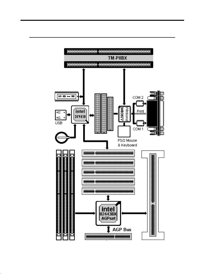
A. Block Diagram
44
Page 46
Technical Information
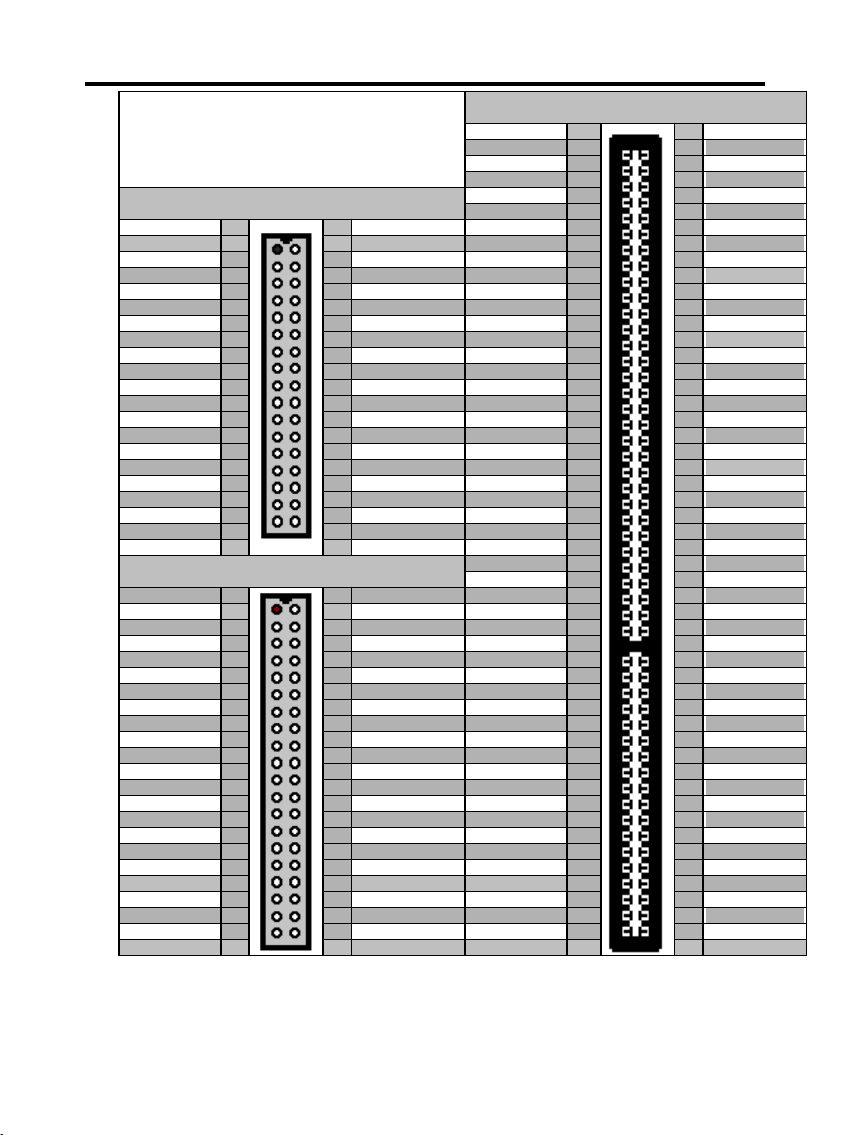
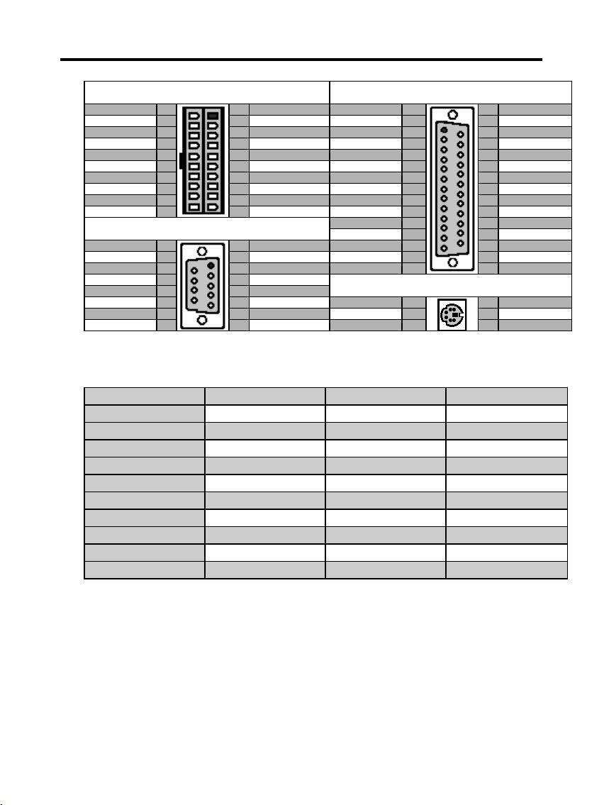
B. I/O Connector Map
ISA Bus
Floppy Disk Connector
IDE Connector
45
Page 47
Technical Information
ATX POWER SUPPLY Connector Parallel port connector
Serial port connector
PS/2 mouse connector signal line
C. The transfer rate of IDE PIO and DMA modes.
Mode PCI Bus Clock Cycle time Data transfer rate
PIO Mode 0 33 MHz 600 ns 3.3 MB/s
PIO Mode 1 33 MHz 383 ns 5.2 MB/s
PIO Mode 2 33 MHz 240 ns 8.3 MB/s
PIO Mode 3 33 MHz 180 ns 11.1 MB/s
PIO Mode 4 33 MHz 120 ns 16.6 MB/s
PIO Mode 5 33 MHz 90 ns 20 MB/s
DMA Mode 0 33 MHz 480 ns 4.16 MB/s
DMA Mode 1 33 MHz 150 ns 13.3 MB/s
DMA Mode 2 33 MHz 120 ns 16.6 MB/s
DMA/33 33 MHz 60 ns 33 MB/s
When IORDY signal is used, PIO Mode 3/4 is in ATA-2 format while
PIO Mode 0/1/2 is in ATA format. PIO Mode5 is unlikely to happen.
46
Page 48
Technical Information
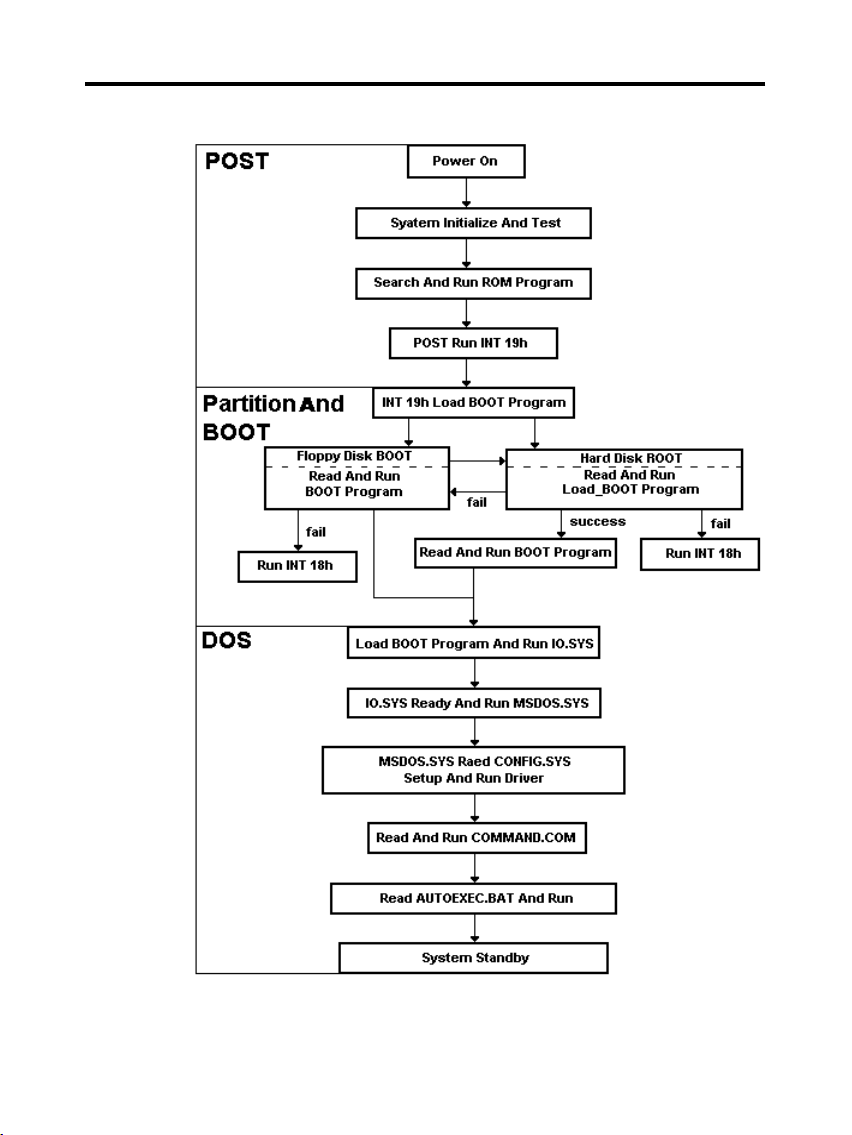
D. The Computer BOOT flow. chart
47
Page 49
Technical Information
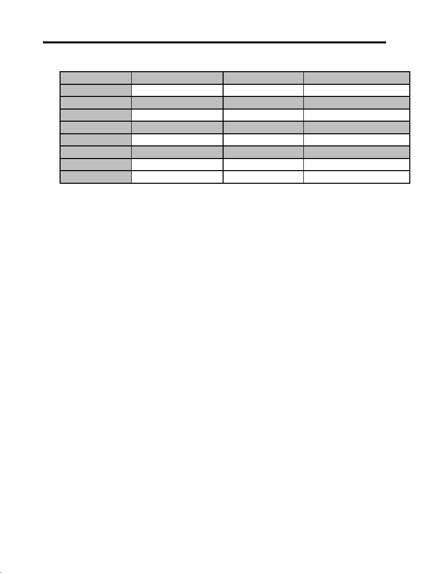
E. The Features Introduction
INTEL 440 BX INTEL i810e VIA 693A+596B
CPU support Pentium II / III Pentium II / III Pentium II / III
Memory size 1GB 1GB 1 GB
Memory SDRAM SDRAM SDRAM
Memory Clock 100 100 100/133MHz
Ex. Clock 66/100MHz 66/100/133MHz 66/100/133 MHz
ACPI Yes Yes ACPI
AGP Bus X 2 X 2 X 4
Ultra ATA/66 No Yes Yes
● Ultra ATA/66
It’s an extension of Ultra ATA33 interface. This new high-speed
interface has doubled the Ultra ATA/33 burst data transfer rate
to 66.6 Mbytes/sec and maximized disk performance under
current PCI local bus environment.
● ACPI (Advanced Configuration and Power Interface)
This Advanced Configuration and Power Interface set up by
Intel, Microsoft, Compaq, IBM, HP….etc, offers the functions
below:
(1) . Automatically stops offering power to CD-ROM, FDD
or HDD when any of them is not in use.
(2) . Offers the “OnNow” function; when you start the
system, what is seen on the screen is in the condition same
as the last time before the system was shut down.
(3) . Enhances the system configuration like PnP, DMI….
● USB(Univer Serial Bus)
The new Bus specification defined by Compaq, DEC, IBM,
Microsoft, NEC, Intel ….etc, is connected by USB, making it
possible for the peripheral to have the “plug and play” function
without interface card.
48
Page 50

Technical Information
There are at most 127 peripherals that can be connected at the
same time.
● Printer Modes /SPP /ECP /EPP
SPP (Standard Parallel Port)
The current commonly used standard mode.
ECP (Extended Capabilities Port)
Jointly set by Microsoft and HP. Its main feature is using highperformance half-duplex bi-directional channel to achieve faster
transmission speed. Its 16-bit FIFO (First-In-First-Out) buffer
makes high-speed transmission more stable and reliable. DMA
function is included in its controller.
EPP (Enhanced Parallel Port)
Jointly set by Intel, Zenith and Xircom. Bi-directional block
transmission makes transmission speed to reach 2MB per
second. It is compatible with the standard parallel port
interface. For printers that do not support the EPP mode in
Windows 95, including the Canon BJ Series and the Epson LQ
Series, you can set the Parallel Mode in BIOS to Normal (SPP)
Mode to enable EPP.
● IrDA (Infrared Data Association)
This organization sets the infrared transmission standards. The
IrDA Protocol sets transmission speed at 115KB per second
and a transmission angle of 30 degree. Its Serial Port shall
have 16550 UARTs and its maximum transmission distance is
one meter.
● S. M. A. R. T (Self Monitoring Analysis Report Technology)
It is jointly set by Conner, IBM, Quantum, Seagate and Western
Digital.
Most hard disks on the market have this function. It issues a
warning
message to the computer user prior to the "actual" failure of the
user can
49
Page 51

Technical Information
have sufficient time to backup data or to replace the hard disk.
F. TIME and DMA CHANNELS MAP
TIME MAP:
TIMER Channel 0 System timer interrupt.
TIMER Channel 1 DRAM REFRESH
request.
TIMER Channel 2 SPEAKER tone
generator.
DMA CHANNELS: DMA Channel 0 Available.
DMA Channel 1 Audio.
DMA Channel 2 FLOPPY DISK.
DMA Channel 3 Onboard ECP
(default).
DMA Channel 4 Cascade.
DMA Channel 5 PCMCIA DMA.
DMA Channel 6 MPEG.
DMA Channel 7 Available.
G. INTERRUPT MAP
NMI: Parity check error.
IRQ (H/W): 0 System TIMER interrupt form TIMER 0.
1 KEYBOARD output buffer full.
2 Cascade for IRQ 8-15.
3 SERIAL port 2.
4 SERIAL port 1.
5 Audio/MPU-401 or PARALLEL port 2.
6 FLOPPY DISK.
7 PARALLEL port 1.
8 RTC clock.
50
Page 52

Technical Information
9 Available.
10 PCMCIA.
11 MPEG.
12 Trackpad (PS/2 Mouse).
13 MATH coprocessor.
14 Primary IDE interface (HDD).
15 Secondary IDE interrface (CD-ROM).
H. RTC and CMOS RAM MAP
RTC and CMOS: 00 Seconds
01 Seconds alarm
02 Minutes
03 Minutes alarm
04 Hours
05 Hours alarm
06 Day of week
07 Day of month
08 Month
09 Year
0A Status register A
0B Status register B
0C Status register C
0D Status register D
0E Diagnostic status byte
0F Shutdown byte
10 FLOPPY DISK drive type byte
11 Reserve
12 HARD DISK type byte
13 Reserve
14 Equipment type
15 Base memory low byte
16 Base memory high byte
17 Extension memory low byte
18 Extension memory high byte
19-2d
2E-2F
51
Page 53

Technical Information
30 Reserved for extension memory
low byte
31 Reserved for extension memory
high byte
32 DATE CENTURY byte
33 INFORMATION FLAG
35-3F Reserve
40-7F Reserved for CHIPSET
SETTING DATA
I. POST Code
POST (HEX) Description
C0 ●●○○
○○○○
1. Turn off OEM specific cache, shadow...
2. Initialize all the standard devices with default values
standard devices including:
- DMA controller (8237)
- Programmable Interrupt Controller (8259)
- Programmable Interval Timer (8254)
C1/C6
● ●○○○○○●╱
●●○○○●●○
Auto-detection of onboard DRAM and Cache
C3 ●●○○
○○●●
1. Test the first 256K DRAM
2. Expand the compressed codes into temporary DRAM area
including the compressed System BIOS and Option ROMs
C5 ●●○○
○●○●
Copy the BIOS from ROM into E0000-FFFFF shadow RAM so that
POST will go faster
01-02
Reserved
03 ○○○○
○○●●
Initialize EISA registers (EISA BIOS ONLY)
04
Reserved
05 ○○○○
○●○●
1. Keyboard Controller Self-Test
2. Enable Keyboard Interface
06 ○○○○
○●●○
F000 shadow R/W test
07 ○○○○
○●●●
Verifies CMOS‘s basfic R/W functionality
BE ●○●●
●●●○
Program defaults values into chipset according to the
MODBINable Chipset Default Table
09 ○○○○
1. Issue CPU ID instruction to idedtify CPU type
52
Page 54

Technical Information
●○○●
2. Program the configuration register of Cyrix CPU according
to the MODBINable Cyrix Register Table
3. OEM specific cache initialization
0A ○○○○
●○●○
1. Initialize the first 32 interrupt vectors with correspoinding
interrupt handlers Initialize INT no from 33-120 with Dummy
(Spurious) Interrupt Handler
2. Early Power Management initialization (OEM specific)
53
Page 55

Technical Information
POST (HEX) Description
0B ○○○○
●○●●
1. Verify whether RTC time is valid or not
2. Detect bad battery
3. Read CMOS data into BIOS stack area
4. PNP initializations including (PNP BIOS ONLY)
- Assign CSN to PNP ISA card
- Create resource map from ESCD
5. Update the P6 CPU‘s micro code (P6 Only)
6. Assign IO and Memory for PCI devices (PCI BIOS ONLY)
0C ○○○○
●●○○
Initialization of the BIOS Data Area (40:0-40:FF)
0D ○○○○
●●○●
1. P5 Multi-P BIOS Only Init IO and Local APIC
2. Program some of the Chipset‘s value according to Setup
(Early Setup Value Program)
3. Measure CPU speed for display and decide system clock
speed
4. Video initialization including Monochrome, CGA, EGA/VGA.
If no display device found, the speaker will beep
0E ○○○○
●●●○
1. Initialize the APIC (Multi-Processor BIOS ONLY)
2. Test video RAM (If Monochrome display device found)
3. Show messages including:
- Award Logo, Copyright String, BIOS Date code and Part No.
- OEM specific sign on messages
- Energy Star Logo (Green BIOS Only)
- CPU brand, type and speed
0F ○○○○
●●●●
DMA channel 0 test
10 ○○○●
○○○○
DMA channel 1 test
11 ○○○●
○○○●
DMA page registers test
12-13
Reserved
14 ○○○●
○●○○
Test 8254 Timer 0 Counter 2
15 ○○○●
○●○●
Test 8259 interrupt mask bits for channel 1
16 ○○○●
○●●○
Test 8259 interrupt mask bits for channel 2
17
Reserved
54
Page 56

Technical Information
POST (HEX) Description
19 ○○○●
●○○●
Test 8259 functionality
1A-1D
Reserved
1E ○○○●
●●●○
If EISA NVM checksum is good,, execute EISA initialization
1F-29
Reserved
30 ○○●●
○○○○
1. Get Base Memory and Extended Memory Size
2. P6 Multi-P BIOS Only Init IO & Local APIC
3. Program K5 CPU‘s Write Allocation
31 ○○●●
○○○●
1. Get Base Memory and Extended Memory Size
2. P6 Multi-P BIOS Only Init IO and Local APIC
3. Program K5 CPU‘s Write Allocation
32 ○○●●
○○●○
1. Display the Award Plug and Play BIOS Extension message
(PNP BIOS ONLY)
2. Program all onboard super I/O chips (if any) including COM
ports, LPT ports, FDD port... according to setup value
3. Program onboard audio devices
33-3B
Reserved
3C ○○●●
●●○○
Set flag to allow users to enter CMOS Setup Utility
3D ○○●●
●●○●
1. Initialize Keyboard
2. Install PS/2 mouse
3. Build the INT 15h function E820H table
4. Build the PnP Device Node for total memory size
3E ○○●●
●●●○
Try to turn on Level 2 cache
Note: Some chipset may need to turn on the L2 cache in this
stage. But usually, the cache is turned on later in POST
61h
3F-40
Reserved
BF ●○●●
●●●●
1. Program the rest of the Chipset‘s value according to setup
2. If auto-configuration is enabled, program the chipset
with predefined values in the MODBIN able Auto-Table
41 ○●○○
○○○●
Initialize floppy disk drive controller
POST (HEX) Description
42 ○●○○
1. Cut IRQ 12 connection if PS/2 mouse is not installed
55
Page 57

Technical Information
○○●○
2. Install IDE Hard Drives
- Auto-detect HDDs
- Build the AT compatible HDD table for Type 47
- Set PIO timing
3. Detect CD ROM on IDE Bus
4. Detect LS120 drive
43 ○●○○
○○●●
If it is a PNP BIOS, initialize serial and parallel ports
44
Reserved
45 ○●○○
○●○●
Initialize math coprocessor
46-4D
Reserved
4E ○●○○
●●●○
1. If there is any error detected (such as video, kb.....), show
all the error messages on the screen and wait for the user to
2. Enable “Far Hit” for Cyrix 6x86 CPU
4F ○●○○
●●●●
1. If password is needed, ask for password
2. Clear the Energy Star Logo (Green BIOS ONLY)
50 ○●○●
○○○○
Write all the CMOS values currently in the BIOS stack area
back into the CMOS
51
Reserved
52 ○●○●
○○●○
1. Initialize all ISA ROMs
2. Later PCI initializations (PCI BIOS ONLY)
- assign IRQ to PCI devices
- initialize all PCI ROMs
3. Program shadows RAM according to setup settings
4. Program Parity according to Setup setting
5. Power Management Initialization
- Enable/Disable global PM
- APM interface initializtion
53 ○●○●
○○●●
1. If it is NOT a PNP BIOS, initialize serial and parallel port
2. Initialize time value in BIOS data area by translating the
RTC time value into a timer tick value
54-5F
Reserved
60 ○●●○
○○○○
Setup Virus Protection (Boot Sector Protection) functionality
according to setup setting
POST (HEX) Descriptions
61 ○●●○
○○○●
1. Try to turn on Level 2 cache
Note: if L2 cache is already turned on in POST 3D, this part
56
Page 58
Technical Information
will be skipped
2. Set the boot up speed according to setup setting
3. Last chance for chipset initialization
4. Last chance for power Management initialization
(Green BIOS only)
5. Show the system configuration table
62 ○●●○
○○●○
1. Setup daylight saving according to setup value
2. Program the NUM Lock, typmatic rate and typmatic speed
according to setup setting
63 ○●●○
○○●●
1. If there is any changes in the hardware configuration,
update the ESCD information (PNP BIOS ONLY)
2. If there is any changes in the hardware configuration,
update the DMI data pool (DMI BIOS ONLY)
3. Clear memory that have been used
4. Boot system via INT 19h
FF ●●●●
●●●●
System Booting. This means that the BIOS already pass the
control right to the operating system
Unexpected Errors:
POST (HEX) Description
B0 ●○●●
○○○○
If interrupt occurs in protected mode
B1 ●○●●
○○○●
Unclaimed NMI occurs
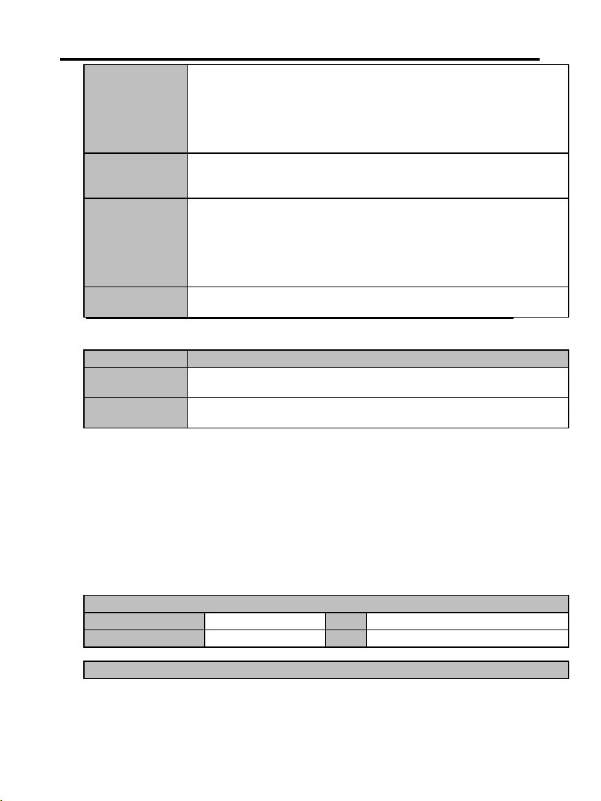
J. Problem Sheet
Customer
Name Tel
address Fax
Mainboard
57
Page 59
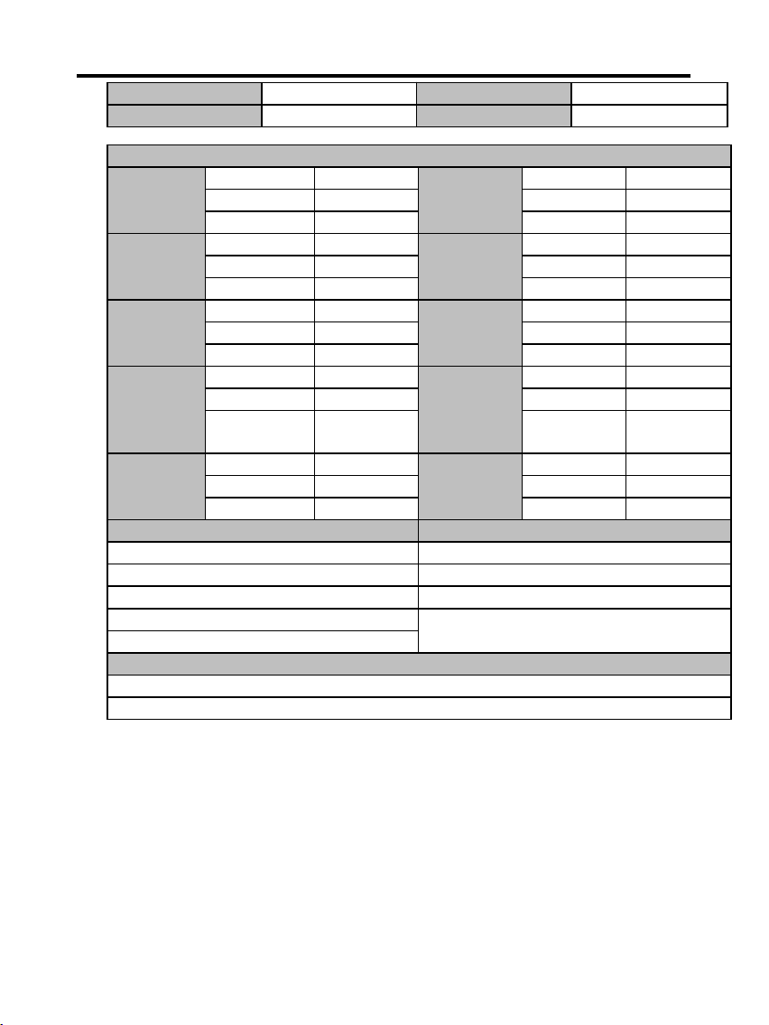
Technical Information
Mode Mainboard Rev
Serial No. BIOS version
Configuration
Brand Brand
CPU Type RAM Type & Size
Voltage Speed
Brand Brand
Floppy disk Mode VGA card Chipset
Size RAM Type
Brand Brand
Hard disk Mode CD-ROM Mode
Size Speed
Brand Brand
Sound card Mode Lan card Mode
Remark PCI/ISA
Bus
Brand Brand
Mouse Mode O.S Name
PS/2 or Serial
Version
Autoexec.bat Config.sys
Problem Description
58
 Loading...