Toshiba ULN 2803 APG, ULN 2804 APG, ULN 2804 AFWG, ULN 2803 AFWG Service Manual

www.DataSheet4U.com
ULN2803,04APG/AFWG
TOSHIBA Bipolar Digital Integrated Circuit Silicon Monolithic
ULN2803APG,ULN2803AFWG,ULN2804APG,ULN2804AFWG
(Manufactured by Toshiba Malaysia)
8ch Darlington Sink Driver
The ULN2803APG / AFWG Series are high−voltage,
high−current darlington drivers comprised of eight NPN
darlington pairs.
All units feature integral clamp diodes for switching inductive
loads.
Applications include relay, hammer, lamp and display (LED)
drivers.
The suffix (G) appended to the part number represents a Lead
(Pb)-Free product.
Features
Output current (single output)
500 mA (Max.)
High sustaining voltage output
50 V (Min.)
Output clamp diodes
Inputs compatible with various types of logic.
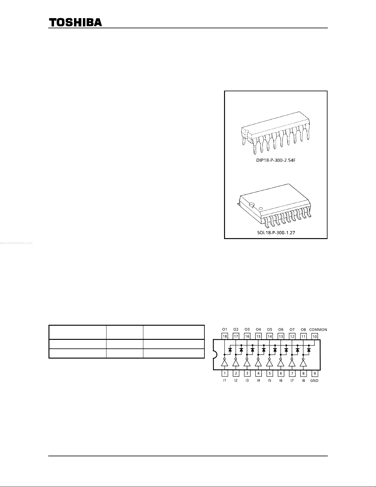
Package Type−APG : DIP−18pin
Package Type−AFWG : SOL−18pin
Pin Connection
ULN2803APG
ULN2804APG
ULN2803AFWG
ULN2804AFWG
Weight
DIP18−P−300−2.54F : 1.478 g (Typ.)
SOL18−P−300−1.27 : 0.48 g (Typ.)
(top view)
Type
ULN2803APG / AFWG 2.7 kΩ TTL, 5 V CMOS
ULN2804APG / AFWG 10.5 kΩ 6~15 V PMOS, CMOS
Input Base
Resistor
Designation
1
2006-02-15

ULN2803,04APG/AFWG
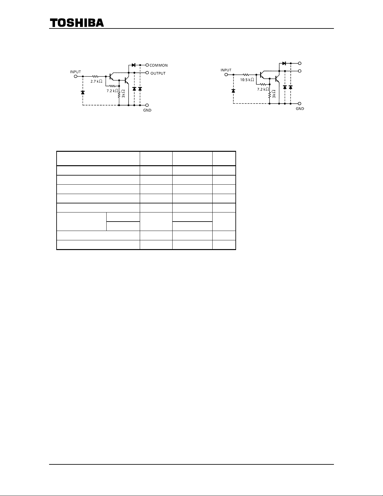
Schematics
(each driver)
ULN2803APG / AFWG ULN2804APG / AFWG
Note: The input and output parasitic diodes cannot be used as clamp diodes.
Absolute Maximum Ratings
Characteristic Symbol Rating Unit
Output sustaining voltage V
Output current I
Input voltage V
Clamp diode reverse voltage V
Clamp diode forward current I
Power dissipation
Operating temperature T
Storage temperature T
APG 1.47
AFWG
(Ta = 25°C)
CE (SUS)
OUT
IN
R
F
P
D
opr
stg
0.92 / 1.31 (Note)
−0.5~50 V
500 mA / ch
−0.5~30 V
50 V
500 mA
W
−40~85 °C
−55~150 °C
Note: On Glass Epoxy PCB (75 × 114 × 1.6 mm Cu 20%)
2
2006-02-15

ULN2803,04APG/AFWG
Recommended Operating Conditions
(Ta = −40~85°C)
Characteristic Symbol Test Condition Min Typ. Max Unit
Output sustaining voltage V
CE (SUS)
APG
Output current
I
AFWG
Input voltage V
Input voltage
(Output on)
ULN2803A 3.5 ― 30
ULN2804A
V
IN (ON)
Clamp diode reverse voltage V
OUT
0 ― 50 V
T
= 25 ms, Duty = 10%,
pw
8 Circuits
T
= 25 ms, Duty = 50%,
pw
8 Circuits
T
= 25 ms, Duty = 10%,
pw
8 Circuits
T
= 25 ms, Duty = 50%,
pw
8 Circuits
0 ― 30 V
IN
8 ― 30
― ― 50 V
R
0 ― 347
0 ― 123
0 ― 268
0 ― 90
Clamp diode forward current IF ― ― 400 mA
Power dissipation
APG Ta = 85°C ― ― 0.76
AFWG
PD
Ta = 85°C (Note) ― ― 0.48
Note: On Glass Epoxy PCB (75 × 114 × 1.6 mm Cu 20%)
mA /
ch
V
W
3
2006-02-15

ULN2803,04APG/AFWG
Electrical Characteristics
(Ta = 25°C)
Test
Characteristic Symbol
Cir−
Cuit
Output leakage current
I
1
CEX
ULN2804A
Collector−emitter saturation voltage VCE (sat)
2
ULN2803A VIN = 3.85 V ― 0.93 1.35
Input current
I
ULN2804A
I
IN (ON)
IN (OFF)
2
4 I
ULN2803A
Input voltage
(Output on)
V
IN (ON)
5
ULN2804A
DC current transfer ratio h
FE
2 VCE = 2 V, I
Clamp diode reverse current IR 6
Clamp diode forward voltage V
Input capacitance C
Turn−on delay t
Turn−off delay t
IN
ON
OFF
F
7 IF = 350 mA ― ― 2.0 V
― ― 15 ― pF
8
Test Condition Min Typ. Max Unit
VCE = 50 V Ta = 25°C ― ― 50
= 50 V Ta = 85°C ― ― 100
V
CE
= 50 V VIN = 1 V ― ― 500
V
CE
I
= 350 mA, IIN = 500 µA ― 1.3 1.6
OUT
I
= 200 mA, IIN = 350 µA ― 1.1 1.3
OUT
I
= 100 mA, IIN = 250 µA ― 0.9 1.1
OUT
VIN = 5 V ― 0.35 0.5
V
= 12 V ― 1.0 1.45
IN
= 500 µA, Ta = 85°C 50 65 ― µA
OUT
VCE = 2 V, I
V
= 2 V, I
CE
V
= 2 V, I
CE
V
= 2 V, I
CE
VCE = 2 V, I
VCE = 2 V, I
V
= 2 V, I
CE
= 200 mA ― ― 2.4
OUT
= 250 mA ― ― 2.7
OUT
= 300 mA ― ― 3.0
OUT
= 125 mA ― ― 5.0
OUT
= 200 mA ― ― 6.0
OUT
= 275 mA ― ― 7.0
OUT
= 350 mA ― ― 8.0
OUT
= 350 mA 1000 ― ―
OUT
Ta = 25°C (Note) ― ― 50
Ta = 85°C (Note) ― ― 100
RL = 125 Ω, V
R
= 125 Ω, V
L
= 50 V ― 0.1 ―
OUT
= 50 V ― 0.2 ―
OUT
µA
V
mA
V
µA
µs
Note: VR = VR MAX.
4
2006-02-15
 Loading...