

Page 1
TXZ Family
© 2018
32-bit RISC Microcontroller
CAN Controller
TXZ Family
Reference Manual
CAN Controller
(CAN-A)
Revision 1.1
2018-10
2018-10-30 1 / 54 Rev. 1.1
Toshiba Electronic Devices & Storage Corporation
Page 2
TXZ Family
CAN Controller
Contents
Preface ................................................................................................................................................................. 5
Related document ..................................................................................................................................................... 5
Conventions ............................................................................................................................................................ 6
Terms and Abbreviations ....................................................................................................................................... 8
1. Outlines ......................................................................................................................................................... 9
2. Block Diagram ............................................................................................................................................. 10
3. Function and Operation .............................................................................................................................. 11
3.1. Clock Supply .................................................................................................................................................... 11
3.2. CAN Interface .................................................................................................................................................. 11
3.3. Function ........................................................................................................................................................... 12
Mailbox ....................................................................................................................................................................... 12
Transmit Control Register ........................................................................................................................................... 13
Receive Control Register ............................................................................................................................................ 14
Remote Frame Control Register ................................................................................................................................. 15
Receive Filtering ......................................................................................................................................................... 16
Time Stamp Function ................................................................................................................................................. 17
Interrupt Control .......................................................................................................................................................... 18
3.4. Operation Mode ............................................................................................................................................... 20
Configuration Mode .................................................................................................................................................... 20
Sleep Mode ................................................................................................................................................................ 22
Suspend Mode ........................................................................................................................................................... 22
Test Loop Back Mode ................................................................................................................................................. 23
Test Error Mode .......................................................................................................................................................... 23
3.5. Bit Configuration .............................................................................................................................................. 25
4. Register ....................................................................................................................................................... 28
4.1. Register list ...................................................................................................................................................... 28
CAN Mailbox............................................................................................................................................................... 29
4.2. Details of Registers .......................................................................................................................................... 30
[CANMBnID]( Message ID Field Register) ................................................................................................................. 30
[CANMBnTSVMCF]( Time Stamp Values Message Control Field Register) .............................................................. 31
[CANMBnDL](Data fields Register ) ........................................................................................................................... 32
[CANMBnDH](Data fields Register) ............................................................................................................................ 32
[CANMC](Mailbox Configuration Register) ................................................................................................................. 33
[CANMD](Mailbox Direction Register) ........................................................................................................................ 33
[CANTRS](Transmission Request Set Register) ........................................................................................................ 34
[CANTRR](Transmission Request Reset Register) .................................................................................................... 35
[CANTA](Transmission Acknow ledge Regist er ) ......................................................................................................... 36
[CANAA](Abort Acknowledge Register) .................................................................................................................... 36
[CANRMP](Receive Message Pending Register) ..................................................................................................... 37
[CANRML](Receive Message Lost Register) ........................................................................................................... 38
2018-10-30 2 / 54 Rev. 1.1
Page 3
TXZ Family
CAN Controller
[CANLAM]( Local Acceptance Mask Register) ......................................................................................................... 39
[CANGAM](Global Acceptance Mask Register)........................................................................................................ 40
[CANMCR](Master Control Register) ........................................................................................................................ 41
[CANGSR](Global Status Register) .......................................................................................................................... 42
[CANBCR1](Bit Configuration Register1) ................................................................................................................. 43
[CANBCR2](Bit Configuration Register2) ................................................................................................................. 43
[CANGIF](Global Interrupt Flag Register) ................................................................................................................. 44
[CANGIM](Global Interrupt Mask Register) .............................................................................................................. 45
[CANMBTIF](Mailbox Transmit Interrupt Flag Register) ........................................................................................... 46
[CANMBRIF](Mailbox Receive Interrupt Flag Register) ............................................................................................ 46
[CANMBIM](Mailbox Interrupt Mask Register) .......................................................................................................... 46
[CANCDR](Change Data Request Register) ............................................................................................................ 47
[CANRFP](Remote Frame Pending Register) .......................................................................................................... 47
[CANCEC](CAN Error Counter Register) ................................................................................................................. 48
[CANTSP](Time Stamp Counter Prescaler Register) ............................................................................................... 49
[CANTSC](Time Stamp Counter Register) ............................................................................................................... 49
5. Usage .......................................................................................................................................................... 50
5.1. Receive Messages ........................................................................................................................................... 50
5.2. Transmitting Message ...................................................................................................................................... 51
5.3. Remote Frame Handling .................................................................................................................................. 52
6. Revision History .......................................................................................................................................... 53
RESTRICTIONS ON PRODUCT USE ............................................................................................................... 54
2018-10-30 3 / 54 Rev. 1.1
Page 4

TXZ Family
CAN Controller
List of Figures
Figure 2.1 Block Diagram of CAN controller ............................................................................................ 10
Figure 3.1 Configurat i on of Mailboxes ..................................................................................................... 12
Figure 3.2 Timing when a Receive Message Lost O ccur s ...................................................................... 14
Figure 3.3 Receive fi lter i ng ...................................................................................................................... 16
Figure 3.4 Timer Sta mp Counter.............................................................................................................. 17
Figure 3.5 Block Diagram of CAN interrupt signals ................................................................................. 19
Figure 3.6 Flowchar t of Initial Setup of CAN Controller ........................................................................... 21
Figure 3.7 Fl owchart of Setup of Test Loop Back Mode and Test Error Mode ............................... 24
Figure 3.8 CAN Bit Tim ing ....................................................................................................................... 25
Figure 5.1 Flowchar t of Message Reception ........................................................................................... 50
Figure 5.2 Flowchar t of M essage Transmission ...................................................................................... 51
Figure 5.3 Flowchar t of Remote Frame Handling Us ing the Automatic Reply Feat ur e .......................... 52
List of Tables
Table 2.1 List of Signa ls ........................................................................................................................... 10
Table 3.1 List of Interrupt sources ........................................................................................................... 18
Table 3.2 Restrictions when Setting the Baud Rate ................................................................................ 26
Table 4.1 Change of [CANRMP] and [CANRML] Registers before/ after a Message is received .......... 38
Table 6.1 Revision History ....................................................................................................................... 53
2018-10-30 4 / 54 Rev. 1.1
Page 5

Preface
Document Name
Clock Control and Operati on M ode
Memory Map
Product Information
Related document
TXZ Family
CAN Controller
2018-10-30 5 / 54 Rev. 1.1
Page 6

Conventions
Numeric formats follow the rules as shown below:
Hexadecimal: 0xABC
Decimal: 123 or 0d123 – Only when it needs to be explicitly shown that they are decimal numbers.
Binary: 0b111 – It is possible to omit the "0b" when the number of bit can be distinctly
understood from a sentence.
"_N" is added to the end of signal names to indicate low active signals.
It is called "assert" that a signal moves to its active level, "deassert" to its inactive level.
When two or more signal names are referred, they are described like as [m: n].
Example: S[3: 0] shows four signal names S3, S2, S1 and S0 together.
The characters surrounded by [ ] defines the register.
Example: [ABCD]
"n" substitutes suffix number of two or more same kind of registers, fields, and bit names.
Example: [XYZ1], [XYZ2], [XYZ3] [XYZn]
"x" substitutes suffix number or character of units and channels in the Register List.
In case of unit, "x" means A, B, and C ...
Example: [ADACR0], [ADBCR0], [ADCCR0] [ADxCR0]
In case of channel, "x" means 0, 1, and 2 ...
Example: [T32A0RUNA], [T32A1RUNA], [T32A2RUNA] [T32AxRUNA]
The bit range of a register is written like as [m: n].
Example: Bit[3: 0] expresses the range of bit 3 to 0.
The configuration value of a register is expressed by either the hexadecimal number or the binary number.
Example: [ABCD]<EFG> =0x01 (hexadecimal), [XYZn]<VW> =1 (binary)
Word and Byte represent the following bit length.
Byte: 8 bits
Half word: 16 bits
Word: 32 bits
Double word: 64 bits
Properties of each bit in a register are expressed as follows:
R: Read only
W: Write only
R/W: Read and Write are possible
Unless otherwise specified, register access supports only word access.
The register defined as reserved must not be rewritten. Moreover, do not use the read value.
The value read from the bit having default value of "-" is unknown.
When a register containing both of writable bits and read-only bits is written, read-only bits should be
written with their default value, In the cases that default is "-", follow the definition of each register.
Reserved bits of the Write-only register should be written with their default value.
In the cases that default is "-", follow the definition of each register.
Do not use read-modified-write processing to the register of a definition which is different by writing and
read out.
TXZ Family
CAN Controller
2018-10-30 6 / 54 Rev. 1.1
Page 7

CAN Controller
***********************************************************************************************************************
***********************************************************************************************************************
Arm, Cortex and Thumb are registered trademarks of Arm Limited (or its s ubs i di ar ies) in the US
and/or elsewhere. All rights reserved.
The Flash memory uses the Super Flash® technology under license from Silicon Storage Technology, Inc.
Super Flash® is registered trademark of Silicon Storage Technology, Inc.
All other company names, product names, and service names mentioned herein may be trademarks of their
respective companies.
TXZ Family
2018-10-30 7 / 54 Rev. 1.1
Page 8

Terms and Abbr e viations
Some of abbreviations used in this document are as follows:
CAN Controller Area Network
TXZ Family
CAN Controller
2018-10-30 8 / 54 Rev. 1.1
Page 9
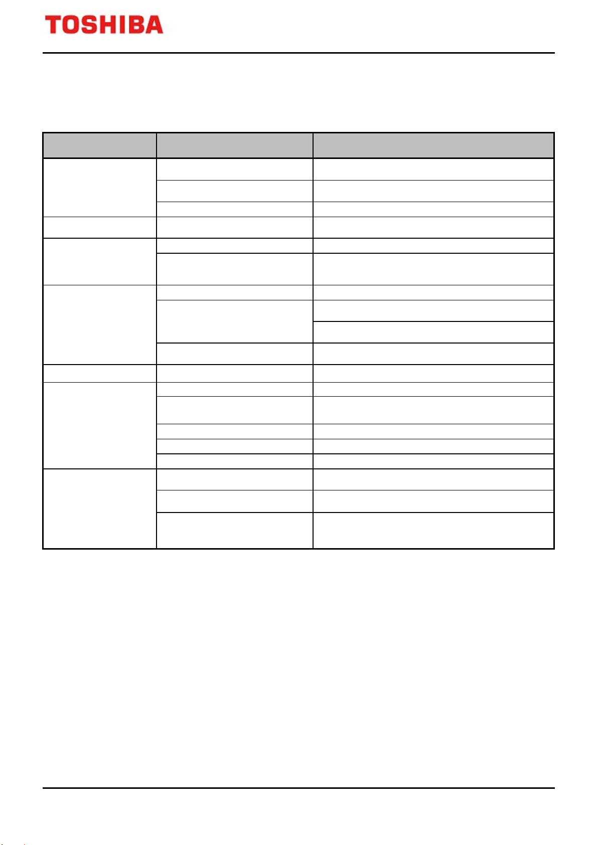
1. Outlines
Function
classification
Function
Operation explanation
Compliant with CAN version 2.0B
active
Standard and extended formats supported
Max 1Mbps(fsys=48MHz(Min))
Baud rate prescaler built in
Equivalent to Intel 82527™
31 reception and transmission
1 reception only
Data Frame / Remote Frame supported
The mailbox with the lower number will be sent first
first
Data Frame / Remote Frame supported
Programmable global receive mas k
(common to mailboxes 0 to 30)
Programmable local receive mask
(for mailbox 31 only)
Standard / Extended ID selection
Receive Mask bit function
Configuration mode
Mode for setting CAN
Suspend mode
Test loop-back mode
Test error mode
CAN Transmit
interrupt(INTCANTXD)
Interrupt when a message transmission is terminated in
normal
CAN Receive
interrupt(INTCANRXD)
Interrupt when a message reception is terminated in
normal
The CAN can operate as a transmission/ reception circuit of 1channel per unit.
The following shows the List of Function.
TXZ Family
CAN Controller
Protocol
Message Box 32 Mailboxes
Transmission
Reception
Time stamp
Operation Mode
CAN bus baud rate
Bit timing parameter
Frame support
Arbitration
Frame support
Masking function
ID format
For Transmission/Reception 16-bit time stamp counter
Sleep mode
The mailbox with the higher priority identifier will be sent
Low power consumption mode( Bus Sleep Mode)
Inactive state on the CAN bus
Self-acknowledge
Writable error counters
Interrupt
CAN Global interrupt (INTCANGLB)
(8 sources)
2018-10-30 9 / 54 Rev. 1.1
Warning level / Error passive / Bus off /
Time stamp overflow/ Transmit abort / Receive message lost/
Wake-up/ Remote frame receive
Page 10
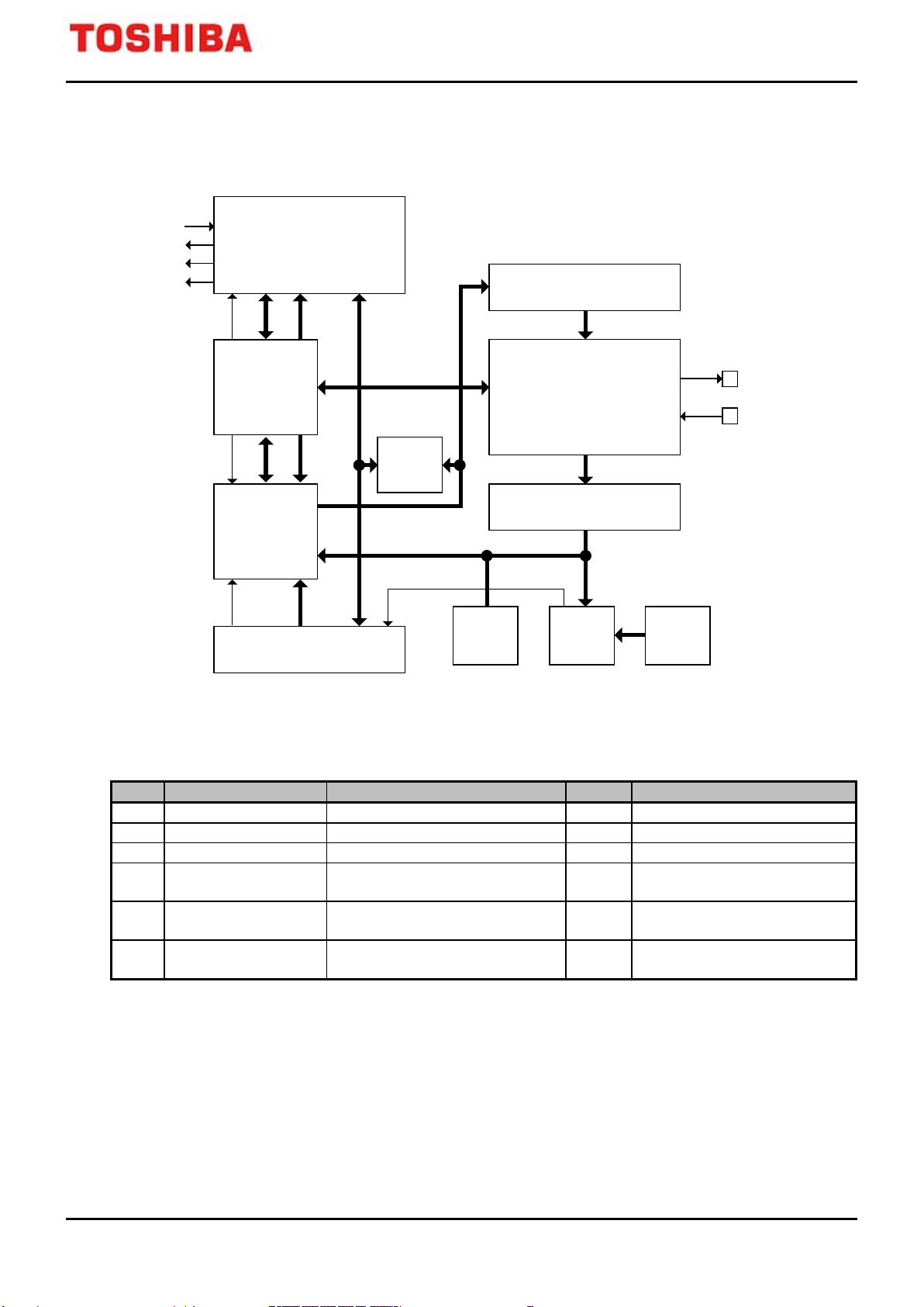
2. Block Diagram
Control & Interrupt
Transmit buffer
Transmit data
CAN protocol controller
R ec e iv e dat a
CPU
interface
CAN state-machine
Mailbox
RAM
(32MailBox)
Receive
mask
CANCLK
INTCANRXD
INTCANTXD
INTCANGLB
Control
R ec e iv e buf fer
Priority
Comarison
register
D ata out p ut
D ata input
ID m atched
CANTX
CANRX
Time
Stamp
counter
Receive
filter
No
Symbol
Signal name
I/O
Related Reference Manual
1
INTCANRXD
CAN receive interrupt
Output
Exception
2
INTCANTXD
CAN transmission interrupt
Output
Exception
3
INTCANGLB
CAN Global interrupt
Output
Exception
Output
Input/Output port, Product
information
Input
Input/Output port, Product
information
Input
Clock Control and Operation
Mode
Figure 2.1 shows the Block Diagram of CAN controller
TXZ Family
CAN Controller
4 CANTX CAN TX signal
5 CANRX CAN RX signal
6 CANCLK CAN clock(f
Figure 2.1 Bloc k Di agram of CAN controller
Table 2.1 List of Si gnals
/4)
sys
2018-10-30 10 / 54 Rev. 1.1
Page 11

TXZ Family
CAN Controller
3. Function and Operation
3.1. Clock Supply
When you use CAN, please set an applicable clock enable bit to "1" (clock supply) in fsys supply stop register A
([CGFSYSENA], [CGFSYSMENA]), fsys supply stop register B ([CGFSYSENB], [CGFSYSMENB]), and fc
supply stop registers ([CGFCEN]).
An applicable register and the bit position vary according to a product. Therefore, the register may not exist with
the product. Please refer to "Clock Control and Operation Mode" of the reference manual for the details.
When attempting to stop supplying the clock, make sure to check whether the CAN is stopping. Note that when
the MCU enters STOP mode, make sure to check whether the CAN is stopping as well.
When fsys clocks of CAN will stop, CANCLK will be stopped.
3.2. CAN Interface
The interface to the CAN bus is an input pin CANRX and an output pin CANTX. Connect these pins via the CAN
bus transceiver (ISO / DIS 11898 compliant).
High speed and low speed transceivers are differentiated. Care must be taken to ensure that the electrical
characteristics of these pins at the chip level (eg, 3.3 V to 5 V) satisfy the requirements of the transceiver.
2018-10-30 11 / 54 Rev. 1.1
Page 12

TXZ Family
D7
D3
TSV1
ID3
D6
D2
TSV0
ID2
D5
D1
D4
D0
MCF
ID0
ID1
MailBox
(CANMBn (n= 0 to 31))
Not used
31 1 6 15 8 7 0
0x0018
0x0010
0x0008
0x0000
Byte3 Byte2 Byte1 Byte0
HalfWord1
Word
HalfWord0
2 4 23
Offset Address
CAN Controller
3.3. Function
Mailbox
The mailboxes consist of a single port RAM (accessible from the internal CAN core and the CPU). The CPU
controls the CAN controller by changing the settings of the mailboxes and control registers. The settings of the
mailboxes and control registers are used for such processes as reception filtering, message transmission, and
interrupt processing.
To start transmission, set the transmission request bit corresponding to the mailbox to be sent. After the bit has
been set, all transmission procedures and error processes (when errors occur) are executed without CPU
involvement. When the mailbox is set to receive, the CPU reads the mailbox data using read instructions.
The user can also set it so that an interrupt will be issued to the CPU every time a message has been successfully
received or transmitted
In total, 32 mailboxes are provided, each of which consists of 8 byte data, 29 bit IDs, and several control bits. The
mailboxes (except mailbox 31) can be set to either transmission or reception. Mailbox 31 is the receive only
mailbox. Mailbox 31 is designed so that it can receive different message ID groups using other receive masks than
mailboxes 0 to 30.
“Figure 3.1” shows the configuration of the mailboxes.
Figure 3.1 Conf igur at io n of Mail boxe s
(1) Message ID field (ID3 to ID0)
‒ ID extension bit <IDE>
‒ Global / local acceptance mask enable bit <GAME_LAME>
‒ Remote frame handling bit<RFH>
‒ 29-bit message ID<ID[28:0]>
(2) Message control field (MCF)
‒ Remote frame transmission request bit<RTR>
‒ Data length of 4 bits<DLC[3:0]>
(3) Time stamp value (TSV1,TSV0)
‒ Stores time stamp counter value during receiving / transmitting message.<TSV[15:0]>
(4) Data field(D7 to D0)
-- Data of 8 bytes <D7[7:0]> to <D0[7:0]>
2018-10-30 12 / 54 Rev. 1.1
Page 13

TXZ Family
CAN Controller
Transmit Control Register
Transmission control consists of two registers. One is the transmission request set register [CANTRS], and the
other is the transmission request reset register [CANTRR]. Therefore it is possible to clear the transmission
request without generating a conflict in the handling of the transmission mailboxes in the state-machine.
This mechanism also prevents clearing the transmission request of a mailbox to which transmission is already in
progress.
When a write of data and the ID to mailbox n configured as a transmission mailbox ([CANMD]<MDn>=0) is
performed and access to mailbox n is enabled ([CANMC]<MCn>=1), setting the [CANTRS]<TRSn> bit to "1"
causes the messages in mailbox n to be transmitted.
If there is more than one mailbox configured as a transmission mailbox and more than one corresponding TRS bit
is set, then the messages will be sent in the selected order. The order of transmission depends on the <MTOS> bit
in the master control register [CANMCR].
If the [CANMCR]<MTOS> bit is "0", the mailbox with the lower number has the higher priority. For example, if
the mailboxes CANMB0, CANMB2, and CANMB5 are configured as transmission mailboxes and the
corresponding
[CANTRS]<TRSn> bits are set to "1", then the messages will be transmitted in the following order:
CANMB0, CANMB2, and CANMB5. If a new transmission request is set for CANMB0 during processing of the
CANMB2 message, then in the next internal arbitration-run, CANMB0 is selected for the next transmission
message and transmission of the CANMB0 message start after CANMB2 transmission is completed.
This will also happen when an arbitration lost error occurs when the CANMB2 message is being transmitted.
The CANMB0 message will be sent instead of the CANMB2 lost in arbitration.
If the [CANMCR]<MTOS> bit is "1", the mailbox with the highest priority ID among those mailboxes for which
transmission is requested will be transmitted. In a transmission after an arbitration lost error occurred also, the
message in the mailbox with the highest priority ID among those mailboxes for which transmission is requested at
the time will be transmitted.
2018-10-30 13 / 54 Rev. 1.1
Page 14

TXZ Family
SOF
Message 1
for m ailbox “n”
EOF IFS SOF
Message 2
for m ailbox “n”
EOF IFS
CAN Bus
Message is valid
Set <RMP>
[CANRMP] register
Set <RML>
[CANRML] register
Co py ID and data to
mailbox
CAN Controller
Receive Control Register
The ID of a received message is compared to the ID of the mailbox set as the receive mailbox. The comparison of
the IDs depends on the [CANMBnID]<GAME_LAME> values of the global/local acceptance mask enable bit and
the data held in the global/local acceptance mask registers [CANGAM]/[CANLAM].
When a match is detected, the ID of the received message, the control bits, and data bytes are written in the
matching mailbox. At the same time, when the corresponding receive message pending bit [CANRMP]<RMPn>
is set to "1" and the mailbox interrupt is enabled ([CANMBIM]<MBIMn>=1), the CAN receive completion
interrupt (INTCANRXD) occurs. After a match is detected, no further ID comparison takes place.
If the ID of the received message does not match with any of the mailboxes 0 to 30, the ID is compared to the ID
of the receive-only mailbox 31. When a match is detected, the settings of the received message are written in
receive-only mailbox 31.
If no match is detected, the received message will not be stored in the mailbox and no change occurs in the
mailbox.
The <RMPn> bit must be cleared by the CPU after data is read. With the <RMPn> bit set to "1", if the next
message to this mailbox n is received, the corresponding receive message lost bit <RMLn> is set to "1".
In this case, mailbox n is overwritten with the new message.
Figure 3.2 shows timing when a receive message lost occurs.
Figure 3.2 Timing wh en a Receive Message Lost Occurs
2018-10-30 14 / 54 Rev. 1.1
Page 15

TXZ Family
CAN Controller
Remote Frame Control Register
After a remote frame is received, the remote frame ID is compared to the mailbox ID. The comparison of the IDs
depends on the [CANMBnID]<GAME_LAME> values of the global/local acceptance mask enable bit
[CANMBnID] in the mailbox and the data held in the global/local acceptance mask registers
[CANGAM]/[CANLAM].
After an ID match is detected, no further comparison takes place.
When the remote frame ID matches with the ID of transmission mailbox n where the remote frame handling bit
[CANMBnID]<RFH> is set to "1", the [CANTRS]<TRSn> bit will be set to "1" so that the message is transmitted
responding to the remote frame. For a transmission mailbox where the [CANMBxID]<RFH> bit is set to "0", the
mailbox does not respond to the remote frame even when the ID matches.
If the ID matches with the ID of receive mailbox n, the received message is handled same as a data frame, and this
sets the [CANRMP]<RMPn> bit and the [CANRMP]<RFPn> bit to "1".
When the remote frame ID matches with the ID of mailbox n where both the [CANMBxID]<RFH> bit and the
global bit are set to "1", the ID of mailbox n is overwritten with the remote frame ID, and the mailbox will
automatically respond to the remote frame using the ID (The <TRSn> bit is set to transmit a data frame).
Therefore, when the global acceptance mask register [CANGAM] is used, one mailbox n may respond to multiple
remote frame IDs depending on the mask value.
2018-10-30 15 / 54 Rev. 1.1
Page 16

TXZ Family
Mailbox ID Receive mask register
Receive message ID
ACR
0
ACR
1
ACR
n
AMR
0
AMR
1
AMR
n
Re c eption request
CAN Controller
Receive Filtering
For mailboxes 0 to 30, the global acceptance mask register [CANGAM] will be used if the global bit in the
mailbox is set. The receiving message will be stored in the first mailbox with a matching ID. Only if there is no
matching ID in the mailboxes 0 to 30, the receiving message will be compared to the receive-only mailbox
(mailbox 31). If the local bit in mailbox 31 is set, the local acceptance mask register [CANLAM] will be used.
Figure 3.3 shows receive filtering.
Figure 3.3 Receive filtering
2018-10-30 16 / 54 Rev. 1.1
Page 17
TXZ Family
Pre scaler R egi st er
<TSP[3:0]>
Prescaler (4 bit)
Fr ee running
Ti m e S tamp Counter
<TSC[15:0]>
Time Stamp Hold Register
(16 bit)
MC U read /write
CA N bus bit clock
MC U read /write
Transmission/Reception
successful
load
Count-u p clock
MailBox RAM
clear
clear
clear
re-load
Re-load v al ue
Entering sleep mode
Entering configuration mode
Wri t e to pre sca l er
Hardware/Software reset
Hardware/Software reset
Entering sleep mode
Entering configuration mode
Wri t e to pre sca l er
CAN Controller
Time Stamp Function
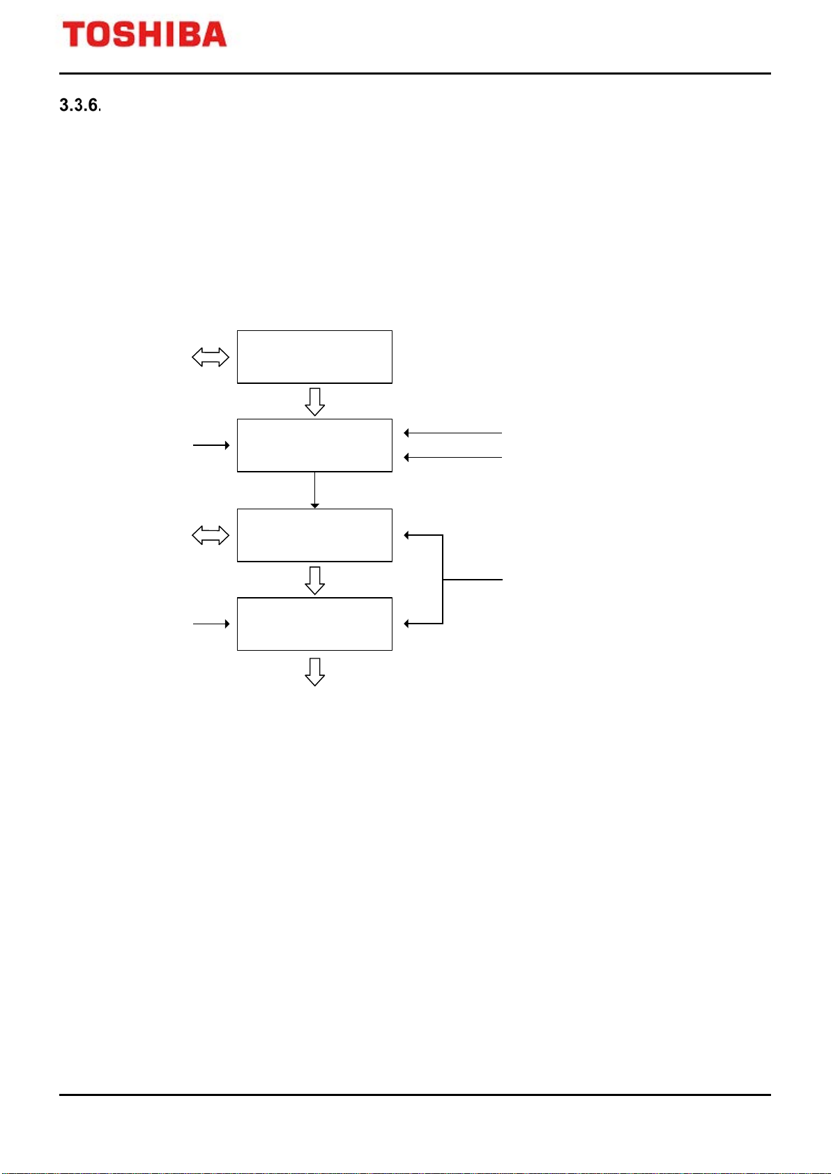
There is a free-running 16-bit time stamp counter [CANTSC] implemented in the CAN controller to show the time
of message reception and transmission. The content of the [CANTSC] is written into the time stamp value (TSV)
of the corresponding mailbox when a received message has been stored or a message has been transmitted.
The [CANTSC] is driven by the bit clock of the CAN bus line. When the operation mode of the CAN is in
configuration mode or in sleep mode, the [CANTSC] will be stopped. After power-up reset, a write to the time
stamp counter prescaler register [CANTSP] clears the [CANTSC] to "0". The [CANTSC] is readable and writable
from the CPU both in configuration mode and normal operation mode.
Figure 3.4 shows the structure of the time stamp counter.
The free running time stamp counter and the time stamp hold register will be cleared in the following cases:
●
●
●
●
2018-10-30 17 / 54 Rev. 1.1
Figure 3.4 Time r St a mp Counter
After reset (Power on reset or software reset)
When the controller enters into configuratio n mode
When the controller enters into sleep mode
When a write access is performed to the [CANTSP] register.
Page 18
TXZ Family
Sources
Group
Transmit interrupt
a message has been transmitted successfully.
INTCANTXD
Receive interrupt
a message has been received successfully.
INTCANRXD
Warning level interrupt
at least one of the two error counters is greater than or equal to 97.
Error passive interrupt
CAN enters the error passive mode.
Bus off interrupt
CAN enters the bus off mode.
Time stamp overflow interrupt
-
Transmit abort interrupt
-
Receive message lost interrupt
-
Walk up interrupt
after walk-up from sleep mode, this interrupt will be generated.
Remote frame receive interrupt
-
CAN Controller
Interrupt Control
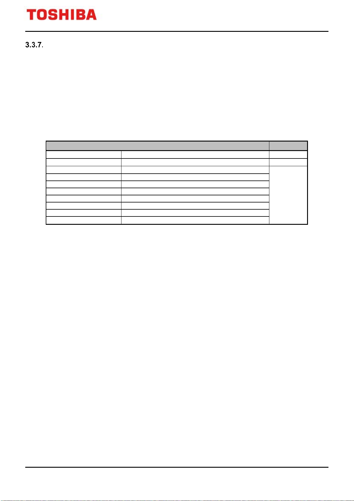
The CAN controller has the following interrupt sources. And these interrupt sources are divided into three groups
and each group has one interrupt output.
● CAN transmission completion interrupt (INTCANTXD)
It occurs at the completion of trans mission
CAN receive completion inter r up t (INTCANRXD)
●
It occurs at the completion of reception
CAN Global interrupt (INTCANGLB)
●
It occurs by eight sources other than those above.
Table 3.1 List of Inte r rupt sources
INTCANGLB
For mailbox interrupts, there are two interrupt output lines separated from global interrupts. These are the mailbox
receive completion interrupt (INTCANRXD) and the mailbox transmission completion interrupt (INTCANTXD),
which are dependent on mailbox settings.
There are two interrupt flag registers and one interrupt mask register. One interrupt flag register is for the mailbox
receive interrupt flag register [CANMBRIF] and one for the mailbox transmission interrupt flag register
[CANMBTIF]. In addition, there is the mailbox interrupt mask register [CANMBIM] for setting whether to
enable or disable each mailbox interrupt. The [CANMBIM] register is used both for transmission and receive
mailboxes.
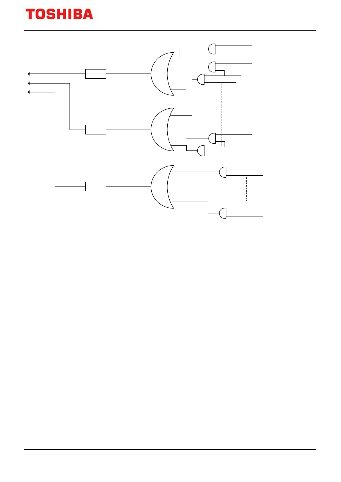
Figure 3.5 shows the block diagram of CAN interrupt signal.
2018-10-30 18 / 54 Rev. 1.1
Page 19
TXZ Family
Pulse
Pulse
Pulse
INTCANRXD
INTCANTXD
INTCANGLB
<MBRIF[31]>
<MBIM[31]>
<MBRIF[30]>
<MBIM[30]>
<MBTIF[30]>
32 sources for
receive
31 sources for
trans mit
<MBRIF[0]>
<MBIM[0]>
<MBTIF[0]>
[CANGIF]<RFPF>
[CANGIM]<RFPM>
8 sources from
global interrupt
[CANGIF]<WLIF>
[CANGIM]<WLIM>
CAN Controller
Figure 3.5 Bloc k Di agram of CAN interrupt signals
The CAN receive completion interrupt signal INTCANRXD is the OR of the signal for which the 32 sources
issued by the mailbox receive interrupt flag register [CANMBRIF] that are ANDed with each bit of the mailbox
interrupt mask register [CANMBIM].
The CAN transmission completion interrupt signal INTCANTXD is the OR of the signal for which the 31 sources
issued by the mailbox transmission interrupt flag register [CANMBTIF] that are ANDed with each bit of the
mailbox interrupt mask register [CANMBIM].
The CAN global interrupt signal INTCANGLB is the OR of the signal for which the 8 sources issued by the
global interrupt flag register [CANGIF] that are ANDed with each bit of the global interrupt mask register
[CANGIM].
2018-10-30 19 / 54 Rev. 1.1
Page 20

TXZ Family
CAN Controller
3.4. Operation Mode
Configuration Mode
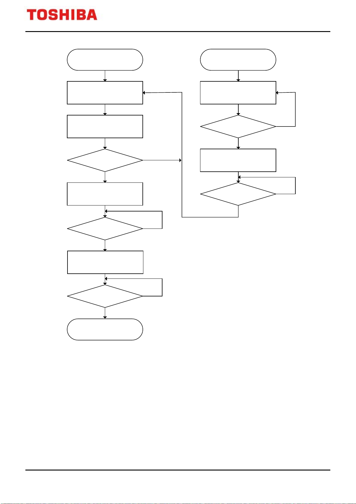
The CAN controller needs initial setup before starting operation (setting of the bit configuration registers,
[CANBCR1] and [CANBCR2]). Writes to the [CANBCR1] and [CANBCR2] are possible only when the CAN
controller is in configuration mode.
After reset, the [CANMCR]<CCR> and the [CANGSR]<CCE> are set to "1" and the configuration mode is set. A
write of "0" to the [CANMCR]<CCR> bit sets the CAN controller to the normal operation mode. After leaving
configuration mode, the [CANGSR]<CCE> bit is cleared to "0" and the power-up sequence starts. The power-up
sequence detects 11 consecutive recessive bits on the CAN bus line. After detection, the CAN controller is a bus
on and ready for operation.
A write of "1" to the [CANMCR]<CCR> bit sets the CAN controller to enter configuration mode from normal
operation mode. After the CAN controller has entered configuration mode, the [CANGSR]<CCE> bit is set to "1".
Figure 3.6 shows the flowchart of the initial setup of the CAN controller.
When the CAN controller enters into configuration mode, the CAN error counter [CANCEC], the time stamp
counter [CANTSC], and the time stamp hold registers will be cleared.
2018-10-30 20 / 54 Rev. 1.1
Page 21
TXZ Family
Initialize CAN after reset
CAN is in configuration mode:
[CANMCR]<CCR> = 1 &
[CANGSR]<CCE> = 1
Set bit timing parameters in
[CANBCR1] & [CANBCR2]
Set [CANMCR]<CCR> to “0”
[CANGSR]<CCE> = 0 ?
CAN is bus on and
ready for oper ation
Switch to configuration mode
from normal operation mode
CAN is in normal operation mode:
[CANMCR]<CCR> = 0 &
[CANGSR]<CCE> = 0
Configuration m ode
requested?
Set [CANMCR]<CCR> to “1”
[CANGSR]<CCE> = 1 ?
No
No
No
No
No
Yes
Yes
Yes
Yes
Yes
Normal operation
requested?
CAN is in normal operation mode
and starts power-up sequence
11 consecutive recessive
bi ts d ete c te d?
CAN Controller
Figure 3.6 Flowchart of Initial Setup of CAN Controller
2018-10-30 21 / 54 Rev. 1.1
Page 22

TXZ Family
CAN Controller
Sleep Mode
Sleep mode is requested by a write of “1” to the <SMR> bit in the [CANMCR] register. After the CAN controller
has entered into sleep mode, the [CANGSR]<SMA> bit is set to “1”.
The read value of the [CANGSR] register is “0x0001F040”. This means that there is no message in the
transmission buffer and sleep mode is active where the <SMA> bit is "1". Read values to all other registers deliver
the value “0”. Write accesses to all registers, except the [CANMCR] register, will be denied.
The CAN controller cancels sleep mode (wakes up) and starts the power-up sequence if a write access to the
[CANMCR] register is detected, or there is any bus activity detected on the CAN bus with the
[CANMCR]<WUBA> bit set to "1". The CAN controller waits until detecting 11 consecutive recessive bits on the
CANRX input terminal, after it goes into bus active state. The walk up message is invalid.
In sleep mode, the CAN error counters and all transmission request set[CANTRS]<TRSn> bits and transmission
request reset [CANTRR]<TRRn> bits are cleared. The [CANMCR]<SMR> bit and the [CANGSR]<SMA> bit are
cleared after the CAN controller leaves sleep mode.
If sleep mode is requested while the CAN controller is transmitting a message ([CANMCR]<SMR>=1), the CAN
controller enters sleep mode after any of the following occurs:
● The message has been successfully transmitted.
● The message has been successfully transmitted after an arbitration lost error.
●
The message has been successfully received after an arbitration lost error.
Suspend Mode
The suspend mode is requested by writing “1” to the [CANMCR]<SUR> bit. If the CAN bus line is not idle, the
current message transmission/reception is completed before suspend mode is activated. After the CAN controller
has entered suspend mode, the [CANGSR]<SUA> bit is set to “1”.
In suspend mode, the CAN controller is not active on the CAN bus line. That means neither error frames nor
acknowledgment will be sent. The error counters and the [CANGSR]<EP> bit will not be cleared either.
If suspend mode is requested during the bus off recovery sequence execution, the CAN controller enters suspend
mode after the bus off recovery sequence is finished.
To restart the CAN controller, the [CANMCR]<SUR> bit needs to be programmed to "0". After leaving the bus
off state or the inactive state, the CAN controller restarts the bus off recovery sequence.
The CAN controller cancels suspend mode with a write of "0" to the [CANMCR]<SUR> bit.
2018-10-30 22 / 54 Rev. 1.1
Page 23

TXZ Family
CAN Controller
Test Loop Back Mode
In test loop back mode, the CAN controller can receive its own transmitted message and generates its own
acknowledge bit. No other CAN node is necessary for the operation.
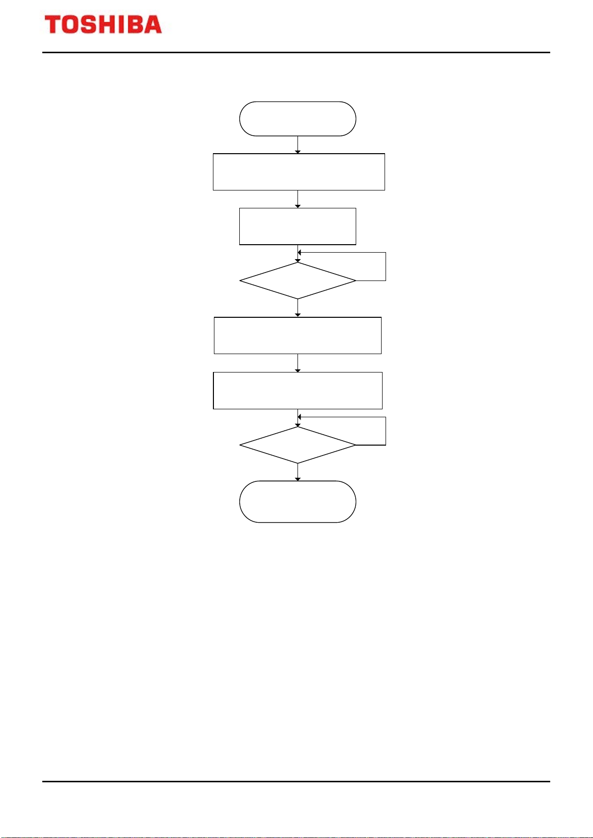
The test loop back mode can be enabled or disabled only when the CAN controller is in suspend mode. In test loop
back mode, the CAN controller can transmit a message from a mailbox and receive it in another mailbox.
The setup for mailbox is the same as in normal operation mode.
Test Error Mode
In test error mode, writes to the CAN error counter register [CANCEC] are possible. The values of the lower 8 bits
are concurrently written to both the transmit error counter (TEC) and the receive error counter (REC). The
maximum value that can be written into the error counters is “255”. The error counter value of “256” which forces
the CAN controller into bus off mode cannot be written.
The test error mode can be enabled or disabled only when the CAN controller is in suspend mode.
Figure 3.7 shows the flowchart of the setup of test loop-back mode and test error mode.
2018-10-30 23 / 54 Rev. 1.1
Page 24
TXZ Family
Enable/disable
test loop bac k mode and
test error mode
CAN is in normal operation mode:
[CANMCR]<CCR> = 0 & [CANGSR]<CCE> = 0
[CANMCR]<SUR> = 0 & [CANGSR]<SUA> = 0
Suspend mode request:
[CANGSR]<SUA> = 1 ?
Back to norm al operation mode with
enabled/disabled [CANMCR]<TSTLB> and/or
[CANMCR]<TSTERR>: set [CANGSR]<SUR> to “0”
[CANGSR]<SUA> = 0 ?
End of setup;
CAN is in normal operation mode
with enabled/disabled test loop
back and/or test error mode
No
No
Yes
Yes
Setup [CANMCR]<TSTLB> and/or
[CANMCR]<TSTERR> bit:
“1” enable,“0” disable
CAN Controller
Figure 3.7 Flowchart of Setu p of Test Loop Back Mode and Test Error Mode
2018-10-30 24 / 54 Rev. 1.1
Page 25
TXZ Family
1 bit time(TBIT)
SYNCSEG
[CANBCR2]
<SJW>
[CANBCR2]
<SJW>
[CANBCR2]<TSEG1> [CANBCR2]<TSEG2>
IPT
Sample point
T
SCL
=
[CANBCR1]<BRP[9:0]>+1
f
CANOSC
BR=
1
(([CANBCR2]<TSEG1[3:0]>+1)+([CANBCR2]<TSEG2[2:0]>+1)+1)×T
SCL
CAN Controller
3.5. Bit Configuration
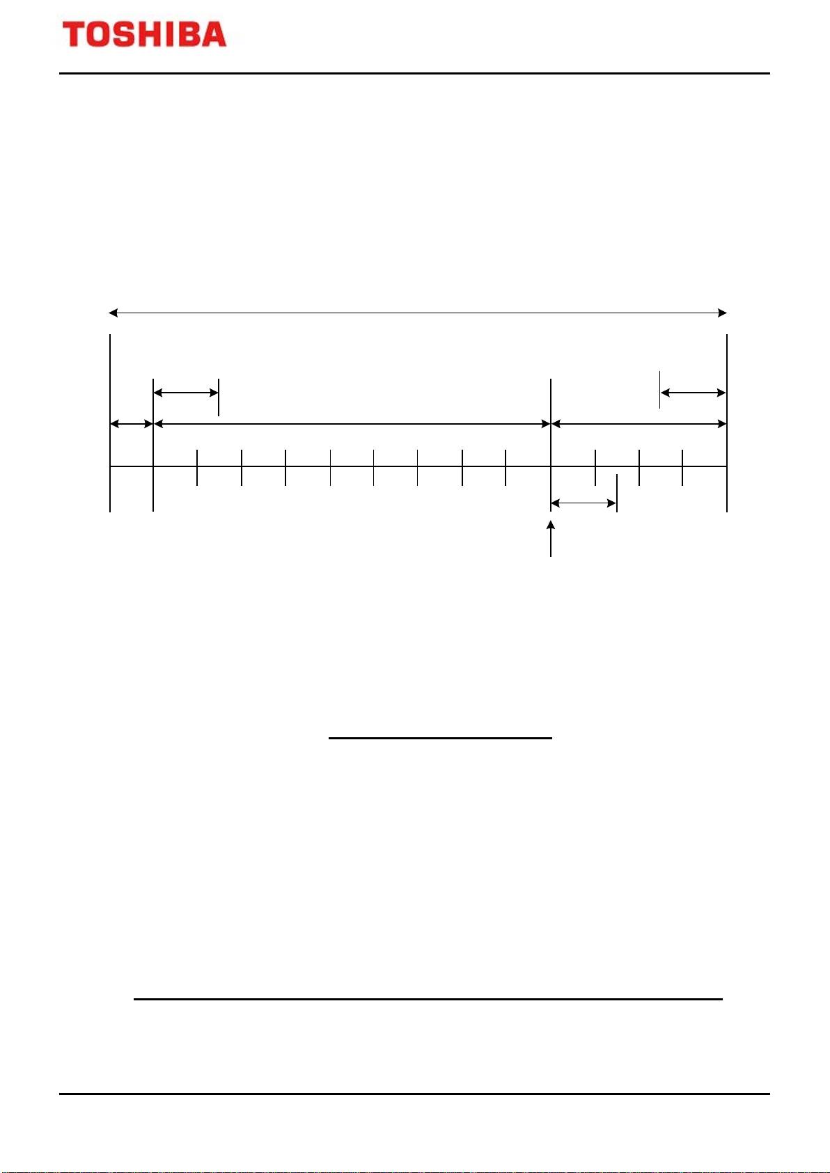
The length of a bit is determined by the parameters [CANBCR2]<TSEG1>, [CANBCR2]<TSEG2>, and
[CANBCR1]<BRP>. All controllers on the CAN bus must have the same baud rate and bit length. At different
clock frequencies of the individual controllers, the baud rate has to be adjusted by the above-mentioned
parameters. In the bit timing logic, the conversion of the parameters to the required bit timing is implemented. The
configuration registers [CANBCR1] and [CANBCR2] contain the data about bit timing. Its definition corresponds
to the CAN specification 2 (equivalent to Intel 82527).
Figure 3.8 shows CAN bit timing.
Figure 3.8 CAN Bit Timing
(CAN system clock) is defined by:
T
SCL
1 × T
= 1 × TQ (TQ: time quantum )
SCL
f
is the clock for CAN baud rate generation. The clock obtained by dividing the system clock f
CANOSC
supplied as the clock for CAN baud rate generation. If f
The synchronization segment SYNCSEG always has the length of one T
= 40MHz then f
SYS
Q
CANOSC
.
= 10MHz.
The baud rate is defined by:
by 4 is
SYS
Note: It is not T
2018-10-30 25 / 54 Rev. 1.1
unit value.
Q
Page 26
TXZ Family
T
(number of CAN clock cycles)
Minimum [CANBCR2]<TSEG2> length
(T
Q
unit)
0
1 3 3
1
2 3 2
> 1
<BRP[9:0]>+1 3 2
CAN Controller
Information processing time (IPT) is the time segment starting with the sample point reserved for processing of
the sampled bit level. The information processing time is equal to three CAN system clock cycles.
[CANBCR2]<SJW[1:0]> indicates how much the time quantum (TQ) value in bit length is allowed to be
lengthened or shortened
When resynchronizing. Values between “1” ([CANBCR2]<SJW[1:0]> = 00) and “4” (<SJW[1:0]> = 11) are
adjustable.
The bus line is sampled and synchronization is performed at each falling edge of the bus signal within a bit grid.
For [CANBCR2]<SJW[1:0]>, set a value equal to or smaller than [CANBCR2]<TSEG2[2:0]>.
Setting the [CANBCR2]<SAM> bit enables the multiple sampling of the bus line. The level is determined by the
result from the majority decision of three sampling values. Sampling is taken at the sample point and the previous
last two CAN system clock points. When [CANBCR1]<BRP[9:0]> is smaller than 4, the sampling performed is
always once regardless of the value set in the [CANBCR2]<SAM> bit.
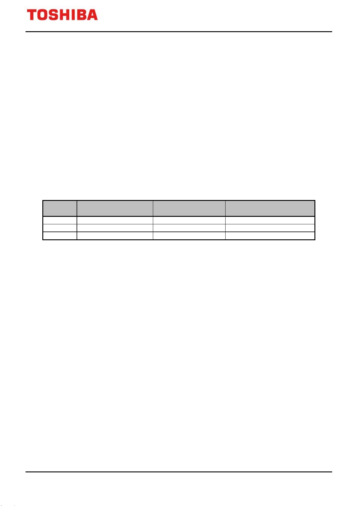
Table 3.2 shows the restrictions when the baud rate is set.
Table 3.2
[CANBCR1]
<BRP[9:0]>
length
Q
Restrictions when Setting the Baud Rate
IPT length
(number of CAN clock cycles)
● Restrictions for [CANBCR2]<TSEG1>
[CANBCR2]<TSEG1> ≥ [CANBCR2]<TSEG2>: The length of <TSEG1> should be equal to or greater
than the length of TSEG2.
Restrictions for [CANBCR2]<SJW>
●
[CANBCR2]<SJW> ≤ [CANBCR2]<TSEG2>: For the synchronization jump width, set a value equal to or
smaller than <TSEG2>.
● Restrictions for
[CANBCR2]<SAM>
The three-time sampling is not allowed under the condition that
For the
condition that [CANBCR1]<BRP[9:0]> < 4, a one-time sampling will always be performed
regardless of the value of SAM.
Example: For 500 Kbit/s
A bit has a length of 2μs. If f
transmission rate has to be programmed with a length of 12T
programmed always are smaller by one than the calculated values:
[CANBCR1]<BRP[9:0]> = 0000000001
[CANBCR2]<TSEG1[3:0]> = 0110 (7T
[CANBCR2]<TSEG2[2:0]> = 011 (4T
In this case, the sample point is 8 / 12 = 66%
Other combinations for [CANBCR2]<TSEG1> / <TSEG2> are possible; with <TSEG2> = 3 the full range for
<SJW>.
[CANBCR1]<BRP[9:0]> is smaller than 4.
= 12 MHz, the baud rate prescaler is set to “1”. That means a bit for this data
CANOSC
According to the above formula, the values to be
.
Q
)
Q
)
Q
2018-10-30 26 / 54 Rev. 1.1
Page 27

TXZ Family
CAN Controller
<SJW> should always be set to the highest value possible. <SJW> is not allowed to be greater than >
<TSEG2>.
The three-time sampling of the bus cannot be set because of the condition that [CANBCR1]<BRP[9:0]> is smaller
than "4".
Thus, <SAM>=0 should be set.
2018-10-30 27 / 54 Rev. 1.1
Page 28

4. Register
Register Name
Address(+Base)
CAN Mailbox
see “4.1.1”
0x0000 to 0x03E0
Mailbox Configuration Register
[CANMC]
0x0400
Mailbox Direction Register
[CANMD]
0x0408
Transmission Request Set Register
[CANTRS]
0x0410
Transmission Request Reset Register
[CANTRR]
0x0418
Transmission Acknowledge Register
[CANTA]
0x0420
Abort Acknowledge Register
[CANAA]
0x0428
Receive Message Pending Register
[CANRMP]
0x0430
Receive Message Lost Register
[CANRML]
0x0438
Local Acceptance Mask Register
[CANLAM]
0x0440
Global Acceptance Mask Register
[CANGAM]
0x0448
Master Control Register
[CANMCR]
0x0450
Global Status Register
[CANGSR]
0x0458
Bit Configuration Register1
[CANBCR1]
0x0460
Bit Configuration Register2
[CANBCR2]
0x0468
Global Interrupt Flag Register
[CANGIF]
0x0470
Global Interrupt Mask Register
[CANGIM]
0x0478
Mailbox Transmit Interrupt Flag register
[CANMBTIF]
0x0480
Mailbox Receive Interrupt Flag register
[CANMBRIF]
0x0488
Mailbox Interrupt Mask Register
[CANMBIM]
0x0490
Change Data Request Register
[CANCDR]
0x0498
Remote Frame Pending Register
[CANRFP]
0x04A0
CAN Error Counter Register
[CANCEC]
0x04A8
Time Stamp Counter Prescaler Register
[CANTSP]
0x04B0
Time Stamp Counter Register
[CANTSC]
0x04B8
4.1. Register list
The control registers and their addresses are shown as follows:
Function Channel/Unit
CAN controller CAN - 0x40005000
TXZ Family
CAN Controller
Base address
TYPE 1
2018-10-30 28 / 54 Rev. 1.1
Page 29
CAN Mailbox
Function name
Mail Box No
Address(+Base)
No.5
0x00A0
No.14
0x01C0
No.25
0x0320
Register Name(n = 0 to 31)
Offset Address
Message ID Field Register
[CANMBnID]
0x0000
Time Stamp Values/ Message Control Filed Register
[CANMBnTSVMCF]
0x0008
Data Filed Register
[CANMBnDL]
0x0010
Data Filed Register
[CANMBnDH]
0x0018
The address of each mailbox is as follows.
TXZ Family
CAN Controller
No.0 0x0000
No.1 0x0020
No,2 0x0040
No.3 0x0060
No.4 0x0080
No.6 0x00C0
No.7 0x00E0
No.8 0x0100
No.9 0x0120
No.10 0x0140
No.11 0x0160
No.12 0x0180
No.13 0x01A0
CAN Mailbox CANMBn
Each of the 32 mailboxes consists of the following field registers.
No.15 0x01E0
No.16 0x0200
No.17 0x0220
No.18 0x0240
No.19 0x0260
No.20 0x0280
No.21 0x02A0
No.22 0x02C0
No.23 0x02E0
No.24 0x0300
No.26 0x0340
No.27 0x0360
No.28 0x0380
No.29 0x03A0
No.30 0x03C0
No.31 0x03E0
2018-10-30 29 / 54 Rev. 1.1
Page 30

4.2. Details of Registers
Bit
Bit Symbol
After Reset
Type
Function
ID Extension bit
the standard format (<IDE>=0).
Global (GAME) / Local (LAME) acceptance mask enable bit
set <GAME> to "0".
Remote frame handling bit (only for transmission mailboxes)
are set.)
Message ID
[CANMBnID]( Message ID Field Register)
0: Standard format (11-bit ID) from <ID28> to <ID18> used
31 IDE - R/W
30 GAME_LAME - R/W
1: Extended format (29-bit ID) from <ID28> to <ID0> used
Sets the mailbox by selecting whether to receive or transmit the extended format (<IDE>=1) or
0: Receive mask is not used for receive filtering.
1: Receive mask is used for receive filtering.
<GAME> is the enable bit for the global acceptance mask GAM shared in mailboxes 0 to 30,
and <LAME> is the enable bit for the local acceptance mask LAM used only for mailbox 31.
When <GAME_LAME>=0, the received message are st ored in the mailbox only when the
receive message ID is the same as the mailbox ID.
For transmission mailboxes, the acceptance mask function is not applied. In such case, always
TXZ Family
CAN Controller
0: Transmit mailboxes do not respond to remote frames. Software must handle remote frames
1: Transmit mailboxes respond to remote frames. (The <TRS> bit is set.)
<RFH> determines whether a mailbox configured as a transmission mailbox will automatically
respond to remote frame reception.
29 RFH - R/W
28:0 ID[28:0] - R/W
When the ID of the received remote frame matches the ID of the transmission mailbox where
<RFH>=1 and <GAME_LAME>=1, this mailbox ID is overwritten with the remote ID, and the
mailbox automatically responds the remote frame using the overwritten ID.
Handled as data frames in the case of receive mailboxes. (The <RMP> bit and the <RFP> bit
Standard format (11-bit ID): From <ID28> to <ID18> are used.
Extended format (29-bit ID): From <ID28> to <ID0> are used.
For the priority of message IDs, the message ID having most "0"s consecutively starting from
the ID’s highest bit (<ID28> bit) has the higher priority.
Register the mailbox IDs at the time of initial setup. To change the message ID field or a mailbox after the
mailbox is enabled, clear the <MCn> bit in the [CANMC] register corresponding to the mailbox to "0", and then
disable the mailbox for the CAN controller before writing a new ID.
2018-10-30 30 / 54 Rev. 1.1
Page 31
[CANMBnTSVMCF]( Time Stamp Values Message Control Field Register)
Bit
Bit Symbol
After Reset
Type
Function
Time stamp counter value
For the details of the entire time s tamp counter function, Refer to “3.3.6Time Stamp Function”.
Remote frame transmission request bit.
1: Remote frame
Data length code
Number
of bytes
0000
0bytes
None
0001
1bytes
D0
0010
2bytes
D0,D1
0011
3bytes
D0,D1,D2
0100
4bytes
D0,D1,D2,D3
0101
5bytes
D0,D1,D2,D3,D4
0110
6bytes
D0,D1,D2,D3,D4,D5
0111
7bytes
D0,D1,D2,D3,D4,D5,D6
1000
8bytes
D0,D1,D2,D3,D4,D5,D6,D7
When <DLC[3:0]> = 1001 or more is set, data length is processed as 8 bytes.
The 16-bit time stamp counter values read when message have been successfully received or
31:16 TSV[15:0] - R/W
15:5 - - R Read as undef i ned.
transmitted are stored. No value is set when message reception or transmission fails.
TXZ Family
CAN Controller
4 RTR - R/W
3:0 DLC[3:0] - R/W
0: Data frame
Sets the data length (number of bytes) of messages
<DLC[3:0]>
Corresponding data
The time stamp values do not need to be initially set.
The message control field needs no initial programming in the case of receive mailboxes. When a received
message is stored in the mailbox, <RTR> and <DLC[3:0]> are also stored in the message control field at the same
time. The transmission mailboxes need initial setting.
To change the message control field of a transmission mailbox (which is set to [CANMBnID]<RFH>=1) after
enabling the mailbox, clear the [CANMC]<MCn> bit to "0" and then disable the mailbox for the CAN controller
before writing a new <RTR> and <DLC[3:0]>. The message control field of the transmission mailbox set to
<RFH>=0 can be changed irrespective of the [CANMC]<MCn> bit setting, but the user needs to check that the
[CANTRS]<TRSn> bit is "0" before writing a new <RTR> and <DLC[3:0]>.
2018-10-30 31 / 54 Rev. 1.1
Page 32
TXZ Family
Bit
Bit Symbol
After Reset
Type
Function
31:24
D3[7:0]
-
R/W
Transmitted and received data is stored.
23:16
D2[7:0]
-
R/W
Transmitted and received data is stored.
15:8
D1[7:0]
-
R/W
Transmitted and received data is stored.
7:0
D0[7:0]
-
R/W
Transmitted and received data is stored.
Bit
Bit Symbol
After Reset
Type
Function
31:24
D7[7:0]
-
R/W
Transmitted and received data is stored.
23:16
D6[7:0]
-
R/W
Transmitted and received data is stored.
15:8
D5[7:0]
-
R/W
Transmitted and received data is stored.
7:0
D4[7:0]
-
R/W
Transmitted and received data is stored.
CAN Controller
[CANMBnDL](Data fields Register )
For transmission, data is transmitted according to the data byte count set in the [CANMBnTSVMCF]<DLC[3:0]>
of the mailbox.
For reception, the data length code in the received message is copied to the [CANMBnTSVMCF]<DLC[3:0]> of
the mailbox, and the data byte count only set in the [CANMBnTSVMCF]<DLC[3:0]> is made valid.
Mailboxes are readable and writable, but do not write data fields for receive mailboxes. If data fields are written, a
mismatch may occur in received data.
To update the data field of a transmission mailbox set to [CANMBnID]<RFH>=1, set "1" in [CANCDR]<CDRn>
and suspend transmission requests temporarily before writing new data. To update the data field of a transmission
mailbox set to [CANMBnID]<RFH>=0, check that the [CANTRS]<TRSn> bit is "0" before writing new data.
[CANMBnDH](Data fields Register)
2018-10-30 32 / 54 Rev. 1.1
Page 33
TXZ Family
Bit
Bit Symbol
After Reset
Type
Function
Access configuration to the mailbox (Each bit corresponds to mailboxes 31 to 0)
Write acces s from CPU
Transmit mailbox
with <RFH>=1
<MCn>=0
Enabled
Enabled
Enabled
Enabled
<MCn>=1
Bit
Bit Symbol
After Reset
Type
Function
Mailbox direction: ( for Mailbox 31)
Mailbox 31 is the receive-only mailbox. This is always set to "1" and cannot be changed.
Mailbox direction: Mailboxes 30 to 0 (Each bit corresponds to mailboxes 30 to 0.)
Each mailbox can be set as a transmission or receive mailbox.
CAN Controller
[CANMC](Mailbox Configuration Register)
0: The corresponding mailbox MBn is disabled for the CAN controller.
1: The corresponding mailbox MBn is enabled for the CAN controller.
31:0 MC[31:0] 0 R/W
ID field
Disabled Disabled Enabled Enabled
Note: the Following care is required during reprogramming of a [CANMC] in operation.
Receive: For a receive mailbox it needs to be ensured that the mailbox is not being disabled while a reception for
this mailbox is ongoing. If a mailbox is disabled or reconfigured during an ongoing reception, the
current frame might be received.
Transmit: When the CAN controller is transmitting data ([CANTRS]<TRSn>=1), Clear <MCn> to "0" after the
transmission is completed ([CANTRS]<TRSn>=0).
Data field Control field
[CANMD](Mailbox Direction Register)
31 MD31 1 R
0: Set as a transmission mailbox.
30:0 MD[30:0] 0 R/W
Set the [CANMD] register at the initial setup. The directions of mailboxes cannot be changed when the operation
is ongoing. To change [CANMD] register settings, set the corresponding [CANMC]<MCn> bit to "0" before
making changes.
1: Set as a receive mailbox.
2018-10-30 33 / 54 Rev. 1.1
Page 34

CAN Controller
Bit
Bit Symbol
After Reset
Type
Function
31 - 0
R
Read as "0"
Transmit request set (Each bit corresponds to mailboxes 30 to 0.)
write of "0" from the CPU is invalid.
[CANTRS](Transmission Request Set Register)
Set <TR Sn> requests the message transmission of corresponding mailbox n.
30:0 TRS[30:0] 0 R/W
Note: Mailbox 31 is receive only mailbox.
The transmission request set register can be set by a write of "1" from the CPU to only the [CANTRS]<TRSn>
bits of the mailboxes configured for transmission. The [CANTRS]<TRSn> bits of the mailboxes configured for
reception cannot be set.
The [CANTRS]<TRSn> bit is cleared to "0" when the message has been successfully transmitted or the
transmission request is reset by setting the [CANTRR]<TRRn> bit to "1".
When the transmission fails, the transmission process is repeated until it succeeds or the transmission request is
reset by setting the [CANTRR]<TRRn> bit to "1".
When the [CANTRS]<TRSn> bit is "1", do not write to mailbox n.
When the transmission is requested for multiple mailboxes, the message is transmitted in
accordance with the priority corresponding to the [CANMCR]<MTOS> bit.
A write of "1" from the CPU to mailbox x configured as transmission mailbox can set the bit. A
TXZ Family
2018-10-30 34 / 54 Rev. 1.1
Page 35

TXZ Family
Bit
Bit Symbol
After Reset
Type
Function
31 - 0
R
Read as "0"
Transmit request reset (Each bit corresponds to mailboxes 30 to 0.)
mailbox can set the bit. Write
of "0" from the CPU is invalid.
CAN Controller
[CANTRR](Transmission Request Reset Register)
30:0 TRR[30:0] 0 R/W
Note: Mailbox 31 is receive only mailbox.
The transmission request reset register can be set by a write of "1" from the CPU to only the [CANTRR]<TRRn>
bits of the mailboxes configured for transmission. The [CANTRR]<TRRn> bits of the mailboxes configured for
reception cannot be set.
The [CANTRR]<TRRn> bit is cleared to "0" by the internal logic when the message has been successfully
transmitted or the transmission is aborted. A write of "0" from the CPU is invalid.
When the [CANTRR]<TRRn> bit is "1," do not write to mailbox n.
Setting the [CANTRR]<TRRn> bit cancels the message transmission of mailbox n set by the [CANTRS]<TRSn>
bit, where the operation executed will be any of the following three sequences:
(a) A transmission request of a message has not yet been transmitted.
A transmission request of a message will be cleared immediately.
([CANTRS]<TRSn> = 0, [CANTRR]<TRRn> = 0, [CANAA]<AAn> = 1)
(b) A transmission request of a message is currently being transmitted and an arbitration lost error occurs or
an error is detected on the CAN bus.
A transmission request of a message will be cleared and the transmission will be canceled.
([CANTRS]<TRSn> = 0, [CANTRR]<TRRn> = 0, [CANAA]<AAn> = 1)
(c) A transmission request of a message is currently being transmitted and no arbitration lost error occurs and
no error is detected on the CAN bus.
A transmission request of a message will not be cleared and the transmission will be completed
([CANTRS]<TRSn> = 0, [CANTRR]<TRRn> = 0, [CANTA]<TAn> = 1)
Setting <TRRn> cancels the message transmission of corresponding mailbox n.
A write of "1" from the CPU to mailbox n configured as transmission
2018-10-30 35 / 54 Rev. 1.1
Page 36
TXZ Family
Bit
Bit Symbol
After Reset
Type
Function
31 - 0
R
Read as "0".
Transmission acknowledge (Each bit corresponds to mailboxes 30 to 0)
[CANTRS]<TRSn> bit.
Bit
Bit Symbol
After Reset
Type
Function
31 - 0
R
Read as "0".
Abort acknowledge (Each bit corresponds to mailboxes 30 to 0.)
[CANTRS]<TRSn> bit.
CAN Controller
[CANTA](Transmission Acknowledge Register)
30:0 TA[30:0] 0 R/W
Note: Mailbox 31 is receive only mailbox
The [CANTA]<TAn> bit is set to "1" when a message in mailbox n has been successfully transmitted.
When the mailbox interrupt is enabled by setting the corresponding <MBIMn> bit in the mailbox interrupt mask
register [CANMBIM] to "1", the <MBTIFn> bit of the mailbox transmission interrupt flag register [CANMBTIF]
is set to "1" and the CAN transmission completion interrupt INTCANTXD occurs.
A write of "1" to the <TAn> bit or the [CANTRS]<TRSn> bit from the CPU can clear the <TAn> bit. A write of
"0" to the <TAn> bit or the [CANTRS]<TRSn> bit from the CPU is invalid.
When the message in mailbox n has been successfully transmitted, the <TAn> bit is set to "1".
The <TAn> bit can be cleared by a write of "1" from the CPU to the <TAn> bit or the
[CANAA](Abort Acknowledge Register)
When the message in mailbox n has not been successful l y transmit ted, t he <AAn> bit is set to
30:0 AA[30:0] 0 R/W
Note: Mailbox 31 is receive only mailbox.
The [CANAA]<AAn> bit is set to "1" when a message in mailbox n has not been successfully transmitted.
When [CANGIF]<TRMABF> bit in the global interrupt flag register is also set to "1", and the transmission abort
interrupt is enabled by setting the [CANGIM]<TRAMABM> bit in the global interrupt mask register to "1", the
CAN global interrupt(INTCANGLB) occurs.
A write of "1" to the <AAn> bit or the [CANTRS]<TRSn> bit from the CPU can clear the <AAn> bit. A write of
"0" to the <AAn> bit or the [CANTRS]<TRSn> bit from the CPU is invalid.
"1".
The <AAn> bit can be cleared by a write of "1" from CPU to the < A An> bit or the
2018-10-30 36 / 54 Rev. 1.1
Page 37

TXZ Family
Bit
Bit Symbol
After Reset
Type
Function
Receive message pending (Each bit corresponds to mailboxes 31 to 0.)
, the
After received data is read, a write of "1" to the <RMPn> bit c an clear the <RMPn> bit.
CAN Controller
[CANRMP](Receive Message Pending Register)
31:0 RMP[31:0] 0 R/W
Note: This register cannot use read-modify-write instruction.
The [CANRMP]<RMPn> bit is set to "1" when a message in mailbox n has been successfully received.
When the mailbox interrupt is enabled by setting the corresponding <MBIMn> bit in the mailbox interrupt mask
register [CANMBIM] to "1", the <MBRIFn> bit of the mailbox receive interrupt flag register [CANMBRIF] is set
to "1" and the CAN receive completion interrupt INTCANRXD occurs.
To clear the [CANRMP] <RMPn> bit, write "1" to the [CANRMP]<RMPn> bit from the CPU. A write of "0" to
the [CANRMP]<RMPn> bit from the CPU is invalid.
After a message is received and the content of the received message is written in mailbox n
<RMPn> bits set to "1".
2018-10-30 37 / 54 Rev. 1.1
Page 38
TXZ Family
Bit
Bit Symbol
After Reset
Type
Function
Receive message lost (Each bit corresponds to mailboxes 31 to 0.)
A write of "1" to the <RMPn> bit can clear the <RMLn> bit.
Before Reception
After Reception
<RMPn>
<RMLn>
<RMPn>
<RMLn>
No
match
Don't
care
Don't
care
Don't
care
Don't
care
0 0 1
0
The received message is stored in mailbox n with a matching ID.
1 0 1
1
1 1 1
1
CAN Controller
[CANRML](Receive Message Lost Register)
31:0 RML[31:0] 0 R
The [CANRML]<RMLn> bit is set by the internal logic and can be cleared with a write of "1" to the
[CANRMP]<RMPn> bit from the CPU. The <RMPn> bit is also cleared at the same time. A write of "1" or "0" to
the <RMLn> bit from the CPU is invalid.
With the [CANRMP]<RMPn> bit set to "1", if mailbox n receives the next message, the corresponding <RMLn>
bit in the receive message lost register [CANRML] is set to "1". In this case, mailbox n is overwritten with the
new received message.
When the <TRMABF> bit in the global interrupt flag register [CANGIF] is also set to "1", and the transmission
abort interrupt is enabled by setting the <TRMABM> bit in the global interrupt mask register [CANGIM] to "1",
the CAN global interrupt INTCANGLB occurs.
When the receive message lost interrupt is enabled by setting the <RMLIM> bit in the global interrupt mask
register [CANGIM] to "1", the CAN global interrupt INTCANGLB occurs.
Table 4.1 shows the changes of the [CANRMP] and [CANRML] registers before and after a message is received.
When mailbox n for which the <RMPn> bit is set to "1" receives the next message, the content
of the received message is overwritten to the mailbox n, and the <RMLn> bit is set to "1".
Table 4.1 Change of [CANRMP] and [CANRML] Registers before/ after a Message is received
ID
Match
Received message are not stored in any mailboxes.
The received message is overwritten in mailbox n with a matching ID.
This shows that the previous message was lost.
Operation
2018-10-30 38 / 54 Rev. 1.1
Page 39
TXZ Family
Bit
Bit Symbol
After Reset
Type
Function
Mask of the ID extension bit<IDE> (mailbox 31)
regardless of the <IDE> bit of the mailbox 31.
30:29 - 0
R
Read as "0"
Mask of receive message ID
message.
CAN Controller
[CANLAM]( Local Acceptance Mask Register)
0: Not masked
1: Masked
31 LAMI 0 R/W
28:0 LAM[28:0] 0 R/W
The local acceptance mask register [CANLAM] will only be used for filtering of the receiving message ID for
mailbox 31. This feature allows locally masking to any ID bits of the receiving message for mailbox 31.
In the extended format, < ID[28:0] > and < LAM[28:0] > are used to filtering.
In the standard format, < ID[28:18] > and < LAM[28:18] > are used to filtering.
When the message in a standard format is received, the part of the extended ID (<ID[17:0]>) will become an
undefined value. Therefore, the standard and the extended format cannot be recommended to be received in
alternately the same mailbox.
Please set [CANLAM] when initialization (At the configuration mode) and do not change the setting while
operating.
When the setting is changed while receiving the message, the [CANLAM] value on the way of the setting change
is used to filtering of reception message ID.
In case of <LAMI>=0, the message in the standard or the extended format is received,
according to the <IDE> bit of the mailbox 31.
In case of <LAMI>=1, the message in the standard and the extended format is received,
0: Not masked
The reception message is received when the corresponding bit of reception message ID is the
same as mailbox ID.
1: Masked
The reception message is received regardless of the value of the corresponding bit of reception
2018-10-30 39 / 54 Rev. 1.1
Page 40

TXZ Family
Bit
Bit Symbol
After Reset
Type
Function
Mask of the ID extension bit<IDE> ( mailboxes "0" to "30")
regardless of the <IDE> bit of the mailboxes "0" to "30".
30:29 - 0
R
Read as "0".
Mask of receive message ID
message.
CAN Controller
[CANGAM](Global Acceptance Mask Register)
0: Not masked
1: masked
31 GAMI 0 R/W
28:0 GAM[28:0] 0 R/W
The global acceptance mask register [CANGAM] will be used for filtering of the receiving message ID for
mailbox "0" to "30". This feature allows to globally masking any ID bits of the receiving message for mailbox "0"
to "30".
In the extended format, [CANMBnID]<ID[28:0]> and <GAM[28:0]> are used for filtering.
In the standard format, [CANMNnID]<ID[28:18]> and <GAM[28:18]> are used for filtering.
When the message in the standard format is received, the part of the extended ID (<ID[17:0]>) will become an
undefined value. Therefore, the standard and the extended format cannot be recommended to be received in
alternately the same mailbox.
Please set [CANGAM] during the initialization (At the configuration mode) and do not change the setting during
the operation. When the setting is changed while receiving the message, the [CANGAM] value on the way of the
setting change is used for filtering of reception message ID.
In case if <GAMI> =0, the message of the standard or the extended format is received,
according to the <IDE> bit of the mailboxes "0" to "30".
In case of <GAMI> = 1, the message of the standard and the extended format is received,
0: Not masked
The reception message is received when the corresponding bit of reception message ID is the
same as mailbox ID.
1: Masked
The reception message is received regardless of the value of the corresponding bit of reception
2018-10-30 40 / 54 Rev. 1.1
Page 41
[CANMCR](Master Control Register)
Bit
Bit Symbol
After Reset
Type
Function
31:12 - 0
R
Read as "0".
Suspend mode request
1: Request suspend mode
10 - 0
R
Read as "0".
Test loop back
1: Request test loop back mode (This mode supports stand-alone operation.)
Test error
[CANCEC].
Change configuration request
registers, [CANBCR1] and [CANBCR2].)
Sleep mode request (Note3)
counters and transmission requests are reset.)
5 - 0
R
Read as "0".
Walk-up on bus activity
1: Wakes up by detecting a bus active state or a write access to the [CANMCR].
Mailbox transmission order select
1: Messages in mailboxes are transmitted in descending order of message ID priority.
2 - 0
R
Read as "0".
Time stamp counter clear
Software reset (Note2)
1: Resets the CAN controller by software.
TXZ Family
CAN Controller
11 SUR 0 R/W
9 TSTLB 0 R/W
8 TSTERR 0 R/W
7 CCR 1 R/W
6 SMR 0 R/W
4 WUBA 0 R/W
3 MTOS 0 R/W
W
1 TSCC 0
R Read as always "0".
0: Cancels suspend mode (normal operation)
0: Cancels test loop back mode (normal operation)
0: Cancels test error mode (normal operation)
1: Request test error mode (In this mode, it is possible to write the CAN error counter register
0: Cancels configuration mode (normal operation)
1: Request configuration mode (In this mode, it possible to write the bit configuration
0: Cancels sleep mode (normal operation)
1: Request sleep mode (In this mode, the clock of the CAN controller stops and the error
0: Wakes up only by a write access to the [CANMCR] register.
0: Messages are transmitted in ascending order of mailbox number.
0: Disable
1: Clears the time stamp counter to "0". (Note1)
0: Disable
W
0 SRES 0
R Read as always "0".
Note1: The time stamp counter is also cleared by a write to the [CANTSP] register and a write of "0" to the
[CANTSC] register.
Note2: After software reset, all registers in the CAN must be accessed after the following time.
(1) When communication by CAN bus is not performed, please wait for more than 16 clocks based on fsy s.
(2) When communication by CAN bus is performed, please wait for more than 88 clocks based on fsys.
Note 3: To cancel sleep mode of the CAN operation, check that the [CANGSR]<SMA> bit is "1" before setting
[CANMCR]<SMR> to "0".
2018-10-30 41 / 54 Rev. 1.1
Page 42
[CANGSR](Global Status Register)
Bit
Bit Symbol
After Reset
Type
Function
31:17 - 0
R
Read as "0".
Message in slot
01010: Message for mailbox 10 10101: Message for mailbox 21
Receive mode
1: The CAN c ont roller is receiving a message.
Transmit mode
1: The CAN controller is transmitting a message.
9 - 0
R
Read as "0".
Suspend mode acknowledge
1: The CAN controller is in suspend mode.
Change configuration enable
In this mode, it is possible to write the bit configuration registers, [CANBCR1] and [CANBCR2].
Sleep mode acknowledge
reset.
5:4 - 0
R
Read as "0".
Time stamp overflow
this bit, a clear <TSOIF> bit in t he [CANGIF] register to "0".
Bus off status
After the bus off recovery sequence, the CAN controller automatically enters bus on state.
Error passive status
1: The CAN controller is in error passive mode.
Warning status
level.
16:12 MIS[4:0] 11111 R
TXZ Family
CAN Controller
Indicates the mailbox number of a message located in the transmission buffer.
00000: Message for mailbox 0 01011: Message for mailbox 11 10110: Message for mailbox 22
00001: Message for mailbox 1 01100: Message for mailbox 12 10111: Message for mailbox 23
00010: Message for mailbox 2 01101: Message for mailbox 13 11000: Message for mailbox 24
00011: Message for mailbox 3 01110: Message for mailbox 14 11001: Message for mailbox 25
00100: Message for mailbox 4 01111: Message for mailbox 15 11010: Message for mailbox 26
00101: Message for mailbox 5 10000: Message for mailbox 16 11011: Message for mailbox 27
00110: Message for mailbox 6 10001: Message for mailbox 17 11100: Message for mailbox 28
00111: Message for mailbox 7 10010: Message for mailbox 18 11101: Message for mailbox 29
01000: Message for mailbox 8 10011: Message for mailbox 19 11110: Message for mailbox 30
01001: Message for mailbox 9 10100: Message for mailbox 20 11111: No message
11 RM 0 R
10 TM 0 R
8 SUA 0 R
7 CCE 1 R
6 SMA 0 R
3 TSO 0 R
2 BO 0 R
0: The CAN controller has not received a message.
0: The CAN controller is not transmitt i ng a message.
0: The CAN controller is not in suspend mode.
0: The CAN controller is not in configuration mode.
1: The CAN controller is in configuration mode.
0: The CAN controller is not in sleep mode.
1: The CAN controller is in sleep mode.
In this mode, the clock of the CAN controller stops and the error counters and transmission request are
0: The time stamp counter does not overflow.
1: The time stamp counter has overflowed at least once after this bit was last cleared to "0". To clear
0: In the bus on state (normal operation)
1: In bus off state
When CAN bus errors occur abnormally often and the transmission error counter <TEC> reaches its
limit of 256, the CAN controller enters bus off state. No messages can be transmitted and received,
The error counter is undefined.
1 EP 0 R
0 EW 0 R
0: The CAN controller is not in error passive mode.
0: Both <TEC> and <REC> values are 96 or less.
1: At least one of the <TEC> and <REC> values is greater than 96 and has reached the warning
2018-10-30 42 / 54 Rev. 1.1
Page 43
[CANBCR1](Bit Configuration Register1)
Bit
Bit Symbol
After Reset
Type
Function
31:10 - 0
R
Read as "0".
Set the value of Baud rate prescaler
value: 0 to 1023
Bit
Bit Symbol
After Reset
Type
Function
31:10 - 0
R
Read as "0".
Resynchronization jump width
11: 4 × TQ
Setting sampling count
1: Triple sampling
Setting of bit time after sample point
011: 4 × TQ 111: 8 × TQ
Setting of bit time before sample point (except SYNCSEG).
0111: 8 × TQ 1111: 16 × TQ
9:0 BRP[9:0] 0 R/W
[CANBCR2](Bit Configuration Register2)
00: 1 × TQ
9:8 SJW[1:0] 0 R/W
01: 2 × T
10: 3 × T
Q
Q
TXZ Family
CAN Controller
7 SAM 0 R/W
6:4 TSEG2[2:0] 0 R/W
3:0 TSEG1[3:0] 0 R/W
0: Single sampling
000: reserved 100: 5 × TQ
001: 2 × T
010: 3 × T
0000: reserved 1000: 9 × TQ
0001: 2 × T
0010: 3 × T
0011: 4 × T
0100: 5 × T
0101: 6 × T
0110: 7 × T
For detail, please refer to "3.5 Bit Configuration ".
Q 101: 6 × TQ
Q 110: 7 × TQ
Q 1001: 10 × TQ
Q 1010: 11 × TQ
Q 1011: 12 × TQ
Q 1100: 13 × TQ
Q 1101: 14 × TQ
Q 1110: 15 × TQ
2018-10-30 43 / 54 Rev. 1.1
Page 44
[CANGIF](Global Interrupt Flag Register)
Bit
Bit Symbol
After Reset
Type
Function
31:8 - 0
R
Read as "0".
Remote frame pending flag
"1".
Walk-up interrupt flag
1: Sleep mode has been canceled.
Receive message lost interrupt flag
mailbox.
Transmission abort flag
1: Transport abort has occurred. (At least one bit in the [CANAA] register is set.)
Time stamp counter overflow interrupt flag
1: There was at least one overflow of the time stamp counter after this bit was last cleared.
Bus off interrupt flag
1: The CAN controller is in bus off mode.
Error passive interrupt flag
1: The CAN controller is in error passive mode.
Warning level interrupt flag
1: At least one of the error counters has reached the warning level.
0: No remote frame has been received.
7 RFPF 0 R/W
1: Remote frames have been received. (in the receive mailbox)
This bit will not be set when matching with the transmission mailbox for which the <RFH> bit is
TXZ Family
CAN Controller
6 WUIF 0 R/W
5 RMLIF 0 R/W
4 TRMABF 0 R/W
3 TSOIF 0 R/W
2 BOIF 0 R/W
1 EPIF 0 R/W
0 WLIF 0 R/W
0: In sleep mode or normal operation mode
0: No receive message lost error has occurred.
1: A receive message lost error has occurred in at least one mailbox configured as a receive
0: No transport abort has occurred.
0: No overflow has occurred in the time stamp counter after this bit was last cleared.
0: The CAN controller is in bus on mode.
0: The CAN controller is in error active mode.
0: None of the error counters have reached the warning level.
Each interrupt flag of the global interrupt flag register [CANGIF] will be set to "1" if the corresponding global
interrupt condition has met. When the global interrupt flag is set to "1", if the corresponding bit in the global
interrupt mask register [CANGIM] is "1" (interrupt enabled), the CAN global interrupt (INTCANGLB) will be
"High".
The [CANGIF] register (Lower 8bits) can be cleared by writing "1" to the corresponding bit in the [CANGIF]
register. A write of "0" is invalid.
2018-10-30 44 / 54 Rev. 1.1
Page 45
[CANGIM](Global Interrupt Mask Register)
Bit
Bit Symbol
After Reset
Type
Function
31:8 - 0
R
Read as "0".
Remote frame pending interrupt mask
1: Interrupt enable
Walk-up interrupt mask
1: Interrupt enable
Receive message lost interrupt mask
1: Interrupt enable
Transmit abort interrupt mask
1: Interrupt enable
Time stamp counter overflow interrupt mask
1: Interrupt enable
Bus off interrupt mask
1: Interrupt enable
Error passive interrupt mask
1: Interrupt enable
Warning level interrupt mask
1: Interrupt enable
TXZ Family
CAN Controller
7 RFPM 0 R/W
6 WUIM 0 R/W
5 RMLIM 0 R/W
4 TRMABF 0 R/W
3 TSOIM 0 R/W
2 BOIM 0 R/W
1 EPIM 0 R/W
0 WLIM 0 R/W
0: Interrupt disable
0: Interrupt disable
0: Interrupt disable
0: Interrupt disable
0: Interrupt disable
0: Interrupt disable
0: Interrupt disable
0: Interrupt disable
The global interrupt mask register [CANGIM] controls whether to enable or disable a global interrupt
correspondingly to each interrupt condition of the [CANGIF] register. When the bit in the [CANGIF] register is
"0", the corresponding CAN global interrupt is disabled. When the bit in the [CANGIF] register is "1", the
corresponding CAN global interrupt is enabled.
Reset operation clears all bits in the [CANGIM] register to "0", disabling global interrupts.
2018-10-30 45 / 54 Rev. 1.1
Page 46
CAN Controller
Bit
Bit Symbol
After Reset
Type
Function
31 - 0
R
Read as "0".
Mailbox transmission interrupt flag (Each bit corresponds to mailboxes 30 to 0.)
A write of "0" is invalid.
Bit
Bit Symbol
After Reset
Type
Function
Mailbox receive interrupt flag (Each bit corresponds to mailboxes 31 to 0.)
A write of "0" is invalid.
Bit
Bit Symbol
After Reset
Type
Function
Mailbox interrupt mask
1: Interrupt enabled for corresponding mailbox
[CANMBTIF](Mailbox Transmit Interrupt Flag Register)
When the message in mailbox n has been successfully transmitted and the interrupt
mask of the [CANMBIM] register is enabled (<MBIMn>=1), the <MBTIFn> bit is set to "1"
and the transmission completion interrupt (INTCANTXD) becomes the "High" level.
30:0 MBTIF[30:0] 0 R/W
When [CANMBIM]<MBIMn> bit is "0", the <MBTIFn> bit is not set and INTCANTXD
stays at the "Low" level.
Transmission completion is checked by reading the [CANTA] register.
If even one bit in the [CANMBTIF] register is "1", INTCANTXD is the "High" level.
The <MBTIFn> bit is cleared by a write of "1" to the <MBTIFn> bit from the CPU.
When the mailbox is set to receive, the corresponding bit in the [CANMBTIF] register is read as "0". When the
mailbox is set to transmit, the corresponding bit in the [CANMBRIF] register is read as "0".
[CANMBRIF](Mailbox Receive Interrupt Flag Register)
TXZ Family
When mailbox n has successfully received the message and the interrupt mask of the
[CANMBIM] register is enabled (<MBIMn> = 1), the <MBRIFn> When t he <MBIMn> bit in
31:0 MBRIF[31:0] 0 R/W
the ,[CANMBIM] register is "0", the <MBRIFn> bit is not set and INTCANRXD stays at the
"Low" level. Receive completion is checked by reading the [CANRMP] register.
If even one bit in the [CANMBRIF] register is "1", INTCANRXD is the "High" level.
The <MBRIFn> bit is cleared by a write of "1" to the <MBRIFn> bit from the CPU.
[CANMBIM](Mailbox Interrupt Mask Register)
31:0 MBIM[31:0] 0 R/W
The settings in [CANMBIM] determine, for which mailbox the interrupt generation is enabled or disabled.
If a bit in [CANMBIM] is "0", the interrupt generation for the corresponding mailbox is disabled and if it is "1",
the interrupt generation is enabled. Reset value of [CANMBIM] is "0".
0: Interrupt disabled for corresponding mailbox
2018-10-30 46 / 54 Rev. 1.1
Page 47
TXZ Family
Bit
Bit Symbol
After Reset
Type
Function
31 - 0
R
Read as "0".
Change data request (Each bit corresponds to mailboxes 30 to 0.)
arbitration range.
Bit
Bit Symbol
After Reset
Type
Function
Remote frame pending (Each bit corresponds to mailboxes 31 to 0.)
The <RFPn> bit can be cleared by a write of "1" to the [CANRMP]<RMPn> bit.
CAN Controller
[CANCDR](Change Data Request Register)
When the <CDRn> bit of transmission mailbox n is set to "1", the transmission request of this
mailbox n is ignored.
30:0 CDR[30:0] 0 R/W
Note: Mailbox 31 is receive only mailbox.
The change data request register [CANCDR] is effective when updating the data field of transmission mailbox n
where auto acknowledgment of remote frames is enabled ([CANMBnID]<RFH>=1). Mailbox n enabling
automatic acknowledgment starts message transmission automatically responding to received remote frames and
so may update the data field during message transmission (In such cases, updated data is output midway through
transmission). The update of the data field can be avoided by setting the <CDRn> bit to "1" and temporarily
suspending data transmission.
It means mailbox n for which the [CANTRS]<TRSn> bit and the <CDRn> bit are set will be
excluded from the internal arbitration range and will not be transmitted if transmission has not
started. After the <CDRn> bit is cleared to "0", mailbox n is back to be included in the internal
[CANRFP](Remote Frame Pending Register)
When mailbox n configured as receive mailbox receives a remote frame, the <RFPn> bit and
31:0 RFP[31:0] 0 R/W
The [CANRFP]<RFPn> bit is set by the internal logic and can be cleared with a write of "1" to the
[CANRMP]<RMPn> bit from the CPU. The [CANRMP]<RMPn> bit is also cleared at the same time. A write of
"0" to the [CANRMP]<RMPn> bit and a write of "1" or "0" to the [CANRFP]<RFPn> bit from the CPU are
invalid.
Even when mailbox n with [CANRFP]<RFPn>=1 is overwritten by data frame reception, the [CANRFP]<RFPn>
bit is cleared.
When the remote frame pending interrupt is enabled by setting the <RFPM> bit in the global interrupt mask
register [CANGIM] to "1", the CAN global interrupt (INTCANGLB) occurs.
[CANRMP]<RMPn> bit are set to "1".
2018-10-30 47 / 54 Rev. 1.1
Page 48

TXZ Family
Bit
Bit Symbol
After Reset
Type
Function
31:16 - 0
R
Read as "0".
0
R
8-bit transit error counter (After reset release)
-
W
8-bit transit error counter ([CANMCR]<TSTERR>=1)
0
R
8-bit receive error counter (After reset release)
-
W
8-bit receive error counter ([CANMCR]<TSTERR>=1)
CAN Controller
[CANCEC](CAN Error Counter Register )
15:8 TEC[7:0]
7:0 REC[7:0]
The CAN controller contains two error counters: the receive error counter <REC[7:0]> and the transmission error
counter <TEC[7:0]>. The value of both counters can be read from the CPU. A write access to the error counters is
only possible in test error mode (The <TSTERR> bit in the [CANMCR] register is "1"). In the case of a write to
the [CANCEC] register, the write data to the lower 8 bits <REC[7:0]> is written also to the higher 8 bits
<TEC[7:0]>.
The CAN error counters count up or down according to the CAN Specification 2.0B.
The [CANCEC]<<REC[7:0]> is not increased after exceeding the error passive limit (128). When
[CANCEC]<REC[7:0]>=128, after the correct reception of a message, the [CANCEC]<REC[7:0]> is set to a
value between 119 and 127. After reaching the "bus off" status, the error counters are undefined.
If the status "bus off" is reached, the receive error counter is incremented after 11 consecutive recessive bits on the
bus. If the counter reaches the count 128, the module changes automatically to the status error active.
All internal flags are reset and the error counters will be cleared to "0". The configuration registers keep the
programmed values. The values of the counters are undefined during "bus off" status.
When CAN enters configuration mode, the error counters will be cleared.
2018-10-30 48 / 54 Rev. 1.1
Page 49
TXZ Family
Bit
Bit Symbol
After Reset
Type
Function
31:4 - 0
R
Read as "0".
Time stamp counter prescaler
Sets the value to be loaded to the prescaler for the 4-bit TSC.
Bit
Bit Symbol
After Reset
Type
Function
31:16 - 0
R
Read as "0".
Time stamp counter
Free running 16-bit counter
CAN Controller
[CANTSP](Time Stamp Counter Prescaler Register)
3:0 TSP[3:0] 0 R/W
To ensure that the value of the [CANTSC] will not change during the write cycle to the mailbox, a hold register is
implemented. The value of the [CANTSC] will be copied to the hold register and then written to the mailbox from
the hold register if a message has been received or transmitted successfully. The reception is successful for the
receiver, if there is no error but the last one bit of End-of-frame. Transmission is successful for the transmitter if
there is no error until the last bit of End-of-frame. (Refer to the CAN specification 2.0B).
[CANTSC](Time Stamp Counter Register)
15:0 TSC[15:0] 0 R
The overflow of the [CANTSC] can be detected by the time stamp counter overflow interrupt flag <TSOIF> of the
global interrupt flag register [CANGIF], and the time stamp counter overflow flag <TSO> of the global status
register [CANGSR]. Both flags can be cleared by writing "1" to <TSOIF> in the [CANGIF] register.
There is a 4-bit prescaler for the [CANTSC]. Afte r power -up the time stamp counter is driven directly from the bit
clock ([CANTSP]<TSP[3:0]>=0). The period T
for the time stamp counter will be calculated by the following
TSC
formula:
T
= TBIT × ([CANTSP]<TSP[3:0]> + 1)
TSC
2018-10-30 49 / 54 Rev. 1.1
Page 50
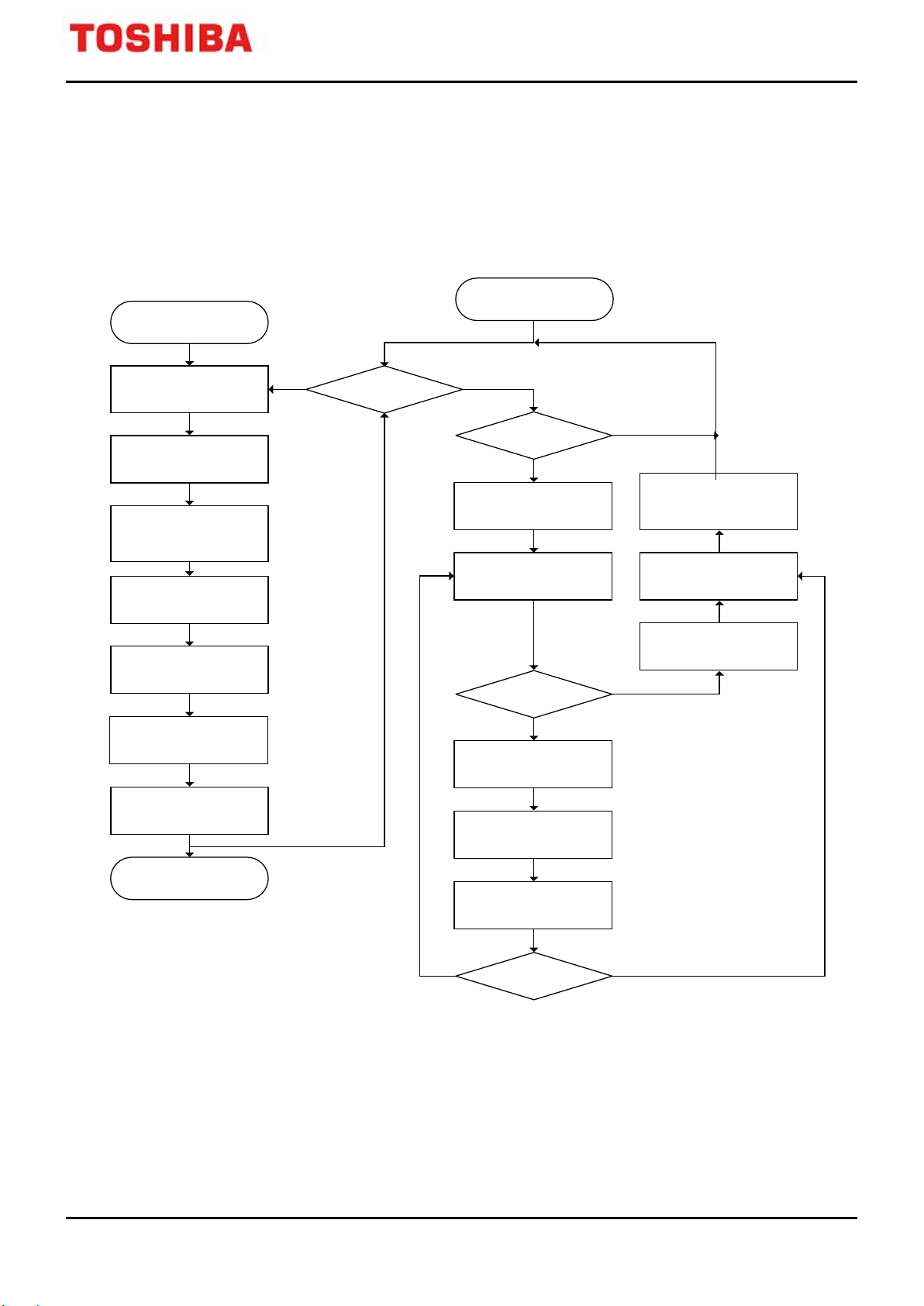
5. Usage
Setup a mailbox for
message reception
Disable mailbox:
set [CANMC]<MCn> to "0"
Configure mailbox for
reception:
set [CANMC]<MDn> to "1"
Setup mailbox identifi er
and [CANMBnID]<IDE> bit for
Standard ID or extended ID
Set
[CANMBnID]<GAME_LAME>
of the mailbox if necessary
Setup [CANLAM]<LAM> /
[CANGAM]<GAM>
If necessary
Enable mailbox:
set [CANMC]<MCn> to "1"
Receiving mess ages
End of setup
New setup for
the mailbox?
Wait for
INTCANRXD
Check [CANRMP]<RMPn> or
[CANMBRIF]<MBRIFn>
to determine the mailbox
Clear [CANMBRIF]<MBRIFn>
and
return from interrupt
service routine
Read out the mai lbox
Special user tasks
Clear [CANRMP]<RMPn>,
this clears also
[CANRML]<RMLn>
[CANRML]<RMLn> = 1?
Data has become inconsistent
reading it out!
Clear [CANRMP]<RMPn>,
this clears also <RMLn>
Read Out Mailbox again
[CANRML]<RMLn> = 1?
Yes
Yes
Yes
Yes No
No
No
No
Enable interrupts:
set [CANMBIM]<MBIMn>
to
"1"
5.1. Receive Messages
Figure 5.1 shows an example flowchart of message reception using the CAN receive completion interrupt
(INTCANRXD).
TXZ Family
CAN Controller
It is also possible to use polling instead of receive interrupts. In this case, the "waiting for INTCANRXD" in
above flowchart must be replaced by polling [CANRMP]. Further, enabling interrupts and clearing [CANMBRIF]
must be removed from the flow.
Figure 5.1 Flowch ar t of Message Reception
2018-10-30 50 / 54 Rev. 1.1
Page 51
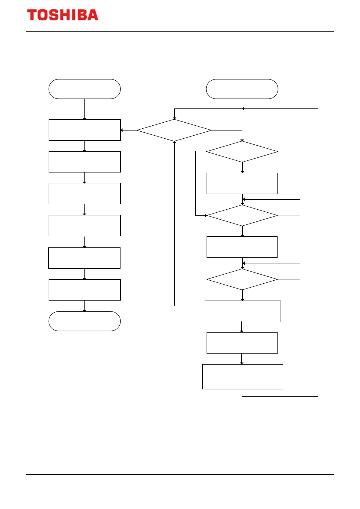
TXZ Family
Setup a mailbox for
message transmission
Enable mailbox:
set [CANMC]<MCn> to "1"
End of setup
New setup for
the mailbox?
Update mailbox
data?
Wait for
INTCANTXD
Yes
Yes
Yes
No
No
Choose transmission order:
setup [CANMCR]<MTOS>
Setup mailbox identifier
and [CANMBnID]<IDE> bit for
Standard ID
or extended ID
Configure mai lbox for
transmission:
set [CANMC]<MDn> to "0"
Disable mailbox:
set [CANMC]<MCn> to "0"
Transmitting messages
Special user tasks
(Update mailbox data ?)
Check [CANTA]<TAn> to determine
the mailbox with <TAn> set
Transmission
requested?
Set transmission r equest:
set [CANTRS]<TRSn> to "1"
Write new data to the mailbox
Yes
No
No
Enable interrupts:
set [CANMBIM]<MBIMn> to "1"
Clear [CANTA]<TAn> and
[CANMBTIF]<MBTIFn>
and return from interrupt
service routine
CAN Controller
5.2. Transmitting Message
Figure 5.2 shows an example flowchart of message transmission using the CAN transmission completion interrupt
(INTCANTXD).
Figure 5.2 Flowch ar t of Message Transmissi on
It is also possible to use polling instead of transmission interrupts. In this case, the "waiting for INTCANTXD" in
above flowchart must be replaced by polling [CANTA]. Further, enabling interrupts and clearing [CANMBTIF]
must be removed from the flow.
2018-10-30 51 / 54 Rev. 1.1
Page 52

CAN Controller
Setup a mailbox for automatic
reply to remote frames
Choose transmission Order:
setup [CANMCR]<MTOS>
End of setup
New setup for
the mailbox?
Update mailbox
data?
Yes
Yes
No
Setup [CANGAM]<GAM> if necessary
Set [CANMBnID]<RFH> bit of the mailbox;
set [CANMBnID]<GAME_LAME> if
necessary
Setup mailbox identifier
and [CANIMBnID]<IDE> bit for
Standard ID or extended ID
Configure mailbox for
transmission:
set [CANMC]<MDn> to "0"
Disable mailbox:
set [CANMC]<MCn> to "0"
Automatic reply to
remote frames
Reset [CANCDR]<CDRn>:
set [CANCDR]<CDRn> to "0"
Change data requested:
set [CANCDR]<CDRn> to "1"
Enable mai lbox:
set [CANMC]<MCn> to "1"
Write new data to the mailbox
No
5.3. Remote Frame Handling
Figure 5.3 shows an example flowchart of remote frame handling by using the automatic reply feature.
This feature is available when the [CANMBnID]<RFH> bit of the transmission mailbox is set to "1". To avoid
data inconsistency when updating the mailbox data, the [CANCDR] register controls transmission during data
update of the mailbox.
TXZ Family
Figure 5.3 Flo wch ar t of Remote Frame Handli ng Using the Automati c R epl y Feature
2018-10-30 52 / 54 Rev. 1.1
Page 53

6. Revision History
Revision
Date
Description
1.0
2018-05-28
New Release
- modified SST Trademark
-Replaced latest RESTRICTIONS ON PRODUCT US E
1.1 2018-10-30
TXZ Family
CAN Controller
Table 6.1 Revision History
-2. Figure 2.1 & Table 2.1 : modif ie d " CANx" to "CAN"
-3.2 Modified “CANxRX” to “CANRX” , Modified “CANxTX” t o
“CANTX”
-3.4.2 Modified “CANxRX” to “CANRX”
-4.2.15 Corrected [CAMCR] to [CANMCR] in <WUBA>
2018-10-30 53 / 54 Rev. 1.1
Page 54

TXZ Family
https://toshiba.semicon-storage.com/
CAN Controller
RESTRICTIONS ON PRODUCT USE
Toshiba Corporation and its subsidiaries and affiliates are collectively referred to as “TOSHIBA”.
Hardware, software and systems described in this document are collectively referred to as “Product”.
• TOSHIBA reserves the right to make changes to the information in this document and related Product without notice.
• Thi s document and any information herein may not be reproduced without prior written permission from TOSHIBA. Even with TOSHIBA's
written permission, reproduction is permissible only if reproduction is without alteration/omission.
• Though TOSHIBA works continually to improve Product's quality and reliability, Product can malfunction or fail. Customers are responsible for
complying with safety standards and for providing adequate desi gns and safeguards f or their hardware, soft ware and systems which
minimize risk and avoid situations in which a malfunction or failure of Product could cause loss of human life, bodily injury or damage to
property, including data loss or corruption. Before customers use the Product, create designs including the Product, or incorporate the
Product into their own applications, customers must also refer to and comply with (a) the latest versions of all relevant TOSHIBA information,
including without limitation, this document, the specifications, the data sheets and applic ation notes for Product and t he prec autions and
conditions set forth in the "TOSHIBA Semiconductor Reliability Handbook" and (b) the instructions for the application with which the Product
will be used with or for. Customers are solely responsible for all aspects of their own product design or applications, including but not limited
to (a) determining the appropriateness of the use of this Product in such design or applications; (b) evaluating and determining the
applicability of any information contained in this document, or in charts, diagrams, programs, algorithms, sample application circuits, or any
other referenced documents; and (c) validating all operating parameters for such designs and applications. TOSHIBA ASSUMES NO
LIABILITY FOR CUSTOMERS' PRODUCT DESIGN OR APPLICATIONS.
• P RO DUCT I S NEITHER INTENDED NOR WARRANTED FOR USE IN EQUIPMENTS OR SYSTEMS THAT REQUIRE
EXTRAORDINARILY HIGH LEVELS OF QUALITY AND/OR RELIABILITY, AND/OR A MALFUNCTION OR FAILURE OF WHICH MAY
CAUSE LOSS OF HUMAN LIFE, BODILY INJURY, SERIOUS PROPERTY DAMAGE AND/OR SERIOUS PUBLIC IMPACT
("UNINTENDED USE"). Except for specific applications as expressly stated i n this document, Uni ntended Us e i ncl udes, without limi tation,
equipment used in nuclear facilities, equipment used in the aerospace industry, lifesaving and/or life supporting medical equipment,
equipment used for automobiles, trains, ships and other transportation, traffic signaling equipment, equipment used to control combustions or
explosions, safety devices, elevators and escalators, and devices related to power plant. IF YOU USE PRODUCT FOR UNINTENDED USE,
TOSHIBA ASSUMES NO LIABILITY FOR PRODUCT. For details, please contact your TOSHIBA sales representative or contact us via our
website.
• Do not disassemble, analyze, reverse-engineer, alter, modify, translate or copy Product, whether in whole or in part.
• P roduct shall not be used for or incorporated into any products or systems whose manufacture, use, or sale is prohibited under any
applicable laws or regulations.
• The i nformation contained herein is presented only as guidance for Product use. No responsibility is assumed by TOSHIBA for any
infringement of patents or any other intellectual property rights of third parties that may result from the use of Product. No license to any
intellectual property right is granted by this document, whether express or implied, by estoppel or otherwise.
• ABSENT A WRITTEN SIGNED AGREEMENT, EXCEPT AS PROVIDED IN THE RELEVANT TERMS AND CONDITIONS OF SALE FOR
PRODUCT, AND TO THE MAXIMUM EXTENT ALLOWABLE BY LAW, TOSHIB A (1) ASSUMES NO LIABILITY WHATSOEVER,
INCLUDING WITHOUT LIMITATION, INDIRECT, CONSEQUENTIAL, SPECIAL, OR INCIDENTAL DAMAGES OR LOSS, INCLUDING
WITHOUT LIMITATION, LOSS OF PROFITS, LOSS OF OPPORTUNITIES, BUSINESS INTERRUPTION AND LOSS OF DATA, AND (2)
DISCLAIMS ANY AND ALL EXPRESS OR IMPLIED WARRANTIES AND CONDITIONS RELATED TO SALE, USE OF PRODUCT, OR
INFORMATION, INCLUDING WARRANTIES OR CONDITIONS OF MERCHANTABILITY, FITNESS FOR A PARTICULAR PURPOSE,
ACCURACY OF INFORMATION, OR NONINFRINGEMENT.
• Do not use or otherwise mak e available Product or related software or technology for any military purposes, including without limitation, for
the design, development, use, stockpiling or manufacturing of nuclear, chemical, or biological weapons or missile technology products (mass
destruction weapons). Product and related software and technology may be controlled under the applicable export laws and regulations
including, without limitation, the Japanese Foreign Exchange and Foreign Trade Law and the U.S. Export Administration Regulations. Export
and re-export of Product or related software or technology are strictly prohibited except in compliance with all applicable export laws and
regulations.
• P l ease contact your TOSHIBA sales representative for details as to environmental matters such as the RoHS compatibility of Product. Please
use Product in compliance with all applicable laws and regulations that regulate the inclusion or use of controlled substances, i ncl udi ng
without limitation, the EU RoHS Directive. TOSHIBA ASSUMES NO LIABILITY FOR DAMAGES OR LOSSES OCCURRING AS A RESULT
OF NONCOMPLIANCE WITH APPLICABLE LAWS AND REGUL ATIONS.
2018-10-30 54 / 54 Rev. 1.1
 Loading...