

Page 1
1 / 107
© 2017-2021
TXZ/TXZ+ Family
Advanced Vector Engine Plus
32-bit RISC Microcontroller
TXZ/TXZ+ Family
Reference Manual
Advanced Vector Engine Plus
(A-VE+-B)
Revision 3.1
2021-02
Toshiba Electronic Devices & Storage Corporation
2021-02-24
Rev. 3.1
Page 2

TXZ/TXZ+ Family
2 / 107
Advanced Vector Engine Plus
Contents
Preface ................................................................................................................................................................. 7
Related document ..................................................................................................................................................... 7
Conventions .............................................................................................................................................................. 8
Terms and Abbreviation .......................................................................................................................................... 10
1. Outlines ....................................................................................................................................................... 11
2. Configuration ............................................................................................................................................... 12
2.1. Configuration of the VE .................................................................................................................................... 12
2.2. Interaction between the VE, PMD, and ADC ................................................................................................... 14
3. Description of Operations ........................................................................................................................... 15
3.1. Clock Supply .................................................................................................................................................... 15
3.2. Schedule Management .................................................................................................................................... 15
3.2.1. Schedule Control ........................................................................................................................................................ 17
3.2.2. Start Control ............................................................................................................................................................... 19
3.2.3. Interrupt Control .......................................................................................................................................................... 20
3.3. Description of Tasks ........................................................................................................................................ 21
3.3.1. Current Control (Task 5) ............................................................................................................................................. 23
3.3.2. SIN/COS calculation (Task 6) ..................................................................................................................................... 29
3.3.3. Output Voltage Transformation (Coordinate Axis Transformation/Phase Transformation) ......................................... 31
3.3.3.1. Output coordinate axis transformation (Task 7) ............................................................................................................. 31
3.3.3.2. Output phase transformation 1 (Space vector transformation) (Task 8) ........................................................................ 32
3.3.3.3. Output phase transformation 2 (Inverse Clarke transformation) (Task 11) .................................................................... 34
3.3.4. Output Control ............................................................................................................................................................ 36
3.3.4.1. Output control 1 (Task 0) ............................................................................................................................................... 36
3.3.4.2. Output control 2 (Task 9) ............................................................................................................................................... 42
3.3.5. Trigger Generation (Task 1) ....................................................................................................................................... 47
3.3.6. Input Process.............................................................................................................................................................. 49
3.3.6.1. Input process 1 (Task 2) ................................................................................................................................................ 49
3.3.6.2. Input process 2 (Task 10) .............................................................................................................................................. 52
3.3.7. Input Current Transformation (Phase Transformation/Coordinate Axis Transformation) ............................................ 56
3.3.7.1. Input phase transformation (Task 3) .............................................................................................................................. 56
3.3.7.2. Input coordinate axis transformation (Task 4)................................................................................................................ 57
3.3.8. Other Tasks ................................................................................................................................................................ 58
3.3.8.1. ATAN2 (Arctangent function 2) (Task 12) ...................................................................................................................... 58
3.3.8.2. SQRT (Square root function) (Task 13) ......................................................................................................................... 59
4. Registers ..................................................................................................................................................... 60
4.1. List of Registers ............................................................................................................................................... 60
4.2. Details of VE Control Registers ....................................................................................................................... 63
4.2.1. [VExEN] (VE Operation Enable/Disable Register) ...................................................................................................... 63
4.2.2. [VExCPURUNTRG] (CPU Start Trigger Selection Register) ...................................................................................... 63
4.2.3. [VExTASKAPP] (Task Selection Register) ................................................................................................................. 64
4.2.4. [VExACTSCH] (Operation Schedule Selection Register) ........................................................................................... 65
2021-02-24
Rev. 3.1
Page 3

TXZ/TXZ+ Family
3 / 107
Advanced Vector Engine Plus
4.2.5. [VExREPTIME] (Operation Schedule Repeat Number Selection Register) ................................................................ 65
4.2.6. [VExTRGMODE] (Start Trigger Mode Setting Register) ............................................................................................. 65
4.2.7. [VExERRINTEN] (Error Interrupt Enable/Disable Setting Register) ............................................................................ 66
4.2.8. [VExCOMPEND] (VE Forcible Termination Register) ................................................................................................. 66
4.2.9. [VExERRDET] (Error Detection Register) .................................................................................................................. 66
4.2.10. [VExSCHTASKRUN] (Schedule Operation Status/Ongoing Task Number Register) ............................................... 67
4.2.11. [VExTMPREG0] (Temporary Registers 0) ................................................................................................................ 67
4.3. Details of Dedicated Registers ........................................................................................................................ 68
4.3.1. [VExMCTLF] (Status Register) ................................................................................................................................... 68
4.3.2. [VExMODE] (Task Control Mode Register) ................................................................................................................ 69
4.3.3. [VExFMODE] (Flow Control Register) ........................................................................................................................ 71
4.3.4. [VExTPWM] (PWM Period Rate setting Register) ...................................................................................................... 72
4.3.5. [VExOMEGA] (Rotational Speed setting Register) ..................................................................................................... 72
4.3.6. [VExTHETA] (Motor Phase setting Register) .............................................................................................................. 73
4.3.7. d-axis/q-axis Current Reference setting Registers ..................................................................................................... 73
4.3.7.1. [VExIDREF] (d-axis Current Reference setting Register) .............................................................................................. 73
4.3.7.2. [VExIQREF] (q-axis Current Reference setting Register) .............................................................................................. 73
4.3.8. d-axis/q-axis Voltage setting Registers ....................................................................................................................... 74
4.3.8.1. [VExVD] (d-axis Voltage setting Register) ..................................................................................................................... 74
4.3.8.2. [VExVQ] (q-axis Voltage setting Register) ..................................................................................................................... 74
4.3.8.3. [VExVDQ] (Voltage Scalar Register) ............................................................................................................................. 74
4.3.8.4. [VExVSLIM] (Voltage Scalar Limitation Register) .......................................................................................................... 75
4.3.9. Coefficient Registers for PI control ............................................................................................................................. 76
4.3.9.1. [VExCIDKI] (d-axis Current Integral Coefficient setting Register for PI control) ............................................................. 76
4.3.9.2. [VExCIDKP] (d-axis Current Proportional Coefficient setting Register for PI control) .................................................... 76
4.3.9.3. [VExCIDKG] (d-axis Coefficient Range setting Register for PI control) .......................................................................... 76
4.3.9.4. [VExCIQKI] (q-axis Current Integral Coefficient setting Register for PI control) ............................................................. 77
4.3.9.5. [VExCIQKP] (q-axis Current Proportional Coefficient setting Register for PI control) .................................................... 77
4.3.9.6. [VExCIQKG] (q-axis Coefficient Range setting Register for PI control) ......................................................................... 77
4.3.9.7. [VExVDIH] (d-axis Voltage Integral component Store Register for PI control (Upper)) .................................................. 78
4.3.9.8. [VExVDILH] (d-axis Voltage Integral component Store Register for PI control (Lower)) ................................................ 78
4.3.9.9. [VExVQIH] (q-axis Voltage Integral component Store Register for PI control (Upper)) .................................................. 78
4.3.9.10. [VExVQILH] (q-axis Voltage Integral component Store Register for PI control (Lower)) .............................................. 78
4.3.10. [VExPIOLIM] (Output Limitation Register for PI control) ........................................................................................... 78
4.3.11. [VExFPWMCHG] (PWM Switching Speed setting Register) .................................................................................... 79
4.3.12. [VExPWMOFS] (PWM Shift 2 Offset Register) ......................................................................................................... 79
4.3.13. SIN/COS Registers ................................................................................................................................................... 80
4.3.13.1. [VExCOS] (Cosine value Register of θ) ....................................................................................................................... 80
4.3.13.2. [VExSIN] (Sine value Register of θ)............................................................................................................................. 80
4.3.13.3. [VExCOSM] (Previous Cosine value Register) ............................................................................................................ 80
4.3.13.4. [VExSINM] (Previous Sine value Register) .................................................................................................................. 80
4.3.14. Sector Information Registers .................................................................................................................................... 81
4.3.14.1. [VExSECTOR] (Sector Information Register) .............................................................................................................. 81
4.3.14.2. [VExSECTORM] (Previous Sector Information Register) ............................................................................................ 81
4.3.15. 3-phase Current Registers ....................................................................................................................................... 82
2021-02-24
Rev. 3.1
Page 4

TXZ/TXZ+ Family
4 / 107
Advanced Vector Engine Plus
4.3.15.1. [VExIAO] (a-phase Zero-Current Register) .................................................................................................................. 82
4.3.15.2. [VExIBO] (b-phase Zero-Current Register) .................................................................................................................. 82
4.3.15.3. [VExICO] (c-phase Zero-Current Register) .................................................................................................................. 82
4.3.15.4. [VExIAADC] (ADC Conversion Result Register for a-phase Current) .......................................................................... 83
4.3.15.5. [VExIBADC] (ADC Conversion Result Register for b-phase Current) .......................................................................... 83
4.3.15.6. [VExICADC] (ADC Conversion Result Register for c-phase Current) .......................................................................... 83
4.3.15.7. [VExIA] (a-phase Current Register) ............................................................................................................................. 83
4.3.15.8. [VExIB] (b-phase Current Register) ............................................................................................................................. 84
4.3.15.9. [VExIC] (c-phase Current Register) ............................................................................................................................. 84
4.3.16. DC Supply Voltage Registers ................................................................................................................................... 85
4.3.16.1. [VExVDC] (DC Supply Voltage Register) .................................................................................................................... 85
4.3.16.2. [VExVDCL] (DC2 Supply Voltage Register)................................................................................................................. 85
4.3.17. d-axis/q-axis Current Registers ................................................................................................................................ 86
4.3.17.1. [VExID] (d-axis Current Register) ................................................................................................................................ 86
4.3.17.2. [VExIQ] (q-axis Current Register) ................................................................................................................................ 86
4.3.18. [VExTADC] (ADC Conversion Time setting Register) .............................................................................................. 87
4.3.19. 3-phase PWM Duty Registers .................................................................................................................................. 88
4.3.19.1. [VExCMPU] (U-phase PWM Duty Register) ................................................................................................................ 88
4.3.19.2. [VExCMPV] (V-phase PWM Duty Register)................................................................................................................. 88
4.3.19.3. [VExCMPW] (W-phase PWM Duty Register) ............................................................................................................... 88
4.3.19.4. [VExMINPLS] (Minimum Pulse Width setting Register) ............................................................................................... 89
4.3.20. PWM Output Limitation Registers ............................................................................................................................. 90
4.3.20.1. [VExPWMMAX] (PWM Upper-Limit setting Register) .................................................................................................. 90
4.3.20.2. [VExPWMMIN] (PWM Lower-Limit setting Register) ................................................................................................... 90
4.3.21. [VExOUTCR] (PMD Output Control Register) .......................................................................................................... 91
4.3.22. Trigger Generation Registers ................................................................................................................................... 93
4.3.22.1. [VExTRGCRC] (Synchronous Trigger Correction setting Register) ............................................................................. 93
4.3.22.2. [VExTRGCMP0] (PMD Trigger 0 Timing setting Register) .......................................................................................... 93
4.3.22.3. [VExTRGCMP1] (PMD Trigger 1 Timing setting Register) .......................................................................................... 93
4.3.22.4. [VExTRGSEL] (Synchronous Trigger Selection setting Register) ................................................................................ 94
4.3.23. [VExEMGRS] (EMG release Register) ..................................................................................................................... 94
4.3.24. [VExDELTA] (Current Declination Angle Register) ................................................................................................... 94
4.3.25. Motor Constant Registers ......................................................................................................................................... 95
4.3.25.1. [VExCPHI] (Motor Interlinkage Magnetic Flux Register) .............................................................................................. 95
4.3.25.2. [VExCLD] (Motor d-axis Inductance Register) ............................................................................................................. 95
4.3.25.3. [VExCLQ] (Motor q-axis Inductance Register) ............................................................................................................. 95
4.3.25.4. [VExCR] (Motor Resistance Register) ......................................................................................................................... 95
4.3.25.5. [VExCPHIG] (Motor Magnetic Flux Range setting Register) ........................................................................................ 96
4.3.25.6. [VExCLG] (Motor Inductance Range setting Register) ................................................................................................ 96
4.3.25.7. [VExCRG] (Motor Resistance Range setting Register) ................................................................................................ 96
4.3.26. [VExVDE] (d-axis Voltage Register for Non-interference Control) ............................................................................ 97
4.3.27. [VExVQE] (q-axis Voltage Register for Non-interference Control) ............................................................................ 97
4.3.28. [VExDTC] (Dead Time Compensation Register) ...................................................................................................... 97
4.3.29. [VExHYS] (Hysteresis Width Register for Current Polarity Determination) ............................................................... 97
4.3.30. [VExHYS2] (Hysteresis Width Register 2 for Current Polarity Determination) .......................................................... 98
4.3.31. [VExDTCS] (Dead Time Compensation Control/Status Register) ............................................................................ 98
2021-02-24
Rev. 3.1
Page 5

TXZ/TXZ+ Family
5 / 107
Advanced Vector Engine Plus
4.3.32. [VExTHTCLP] (Clipped Phase value setting Register) ............................................................................................. 99
4.3.33. 2-phase Voltage Registers ....................................................................................................................................... 99
4.3.33.1. [VExVALPHA] (α-phase Voltage Register) .................................................................................................................. 99
4.3.33.2. [VExVBETA] (β-phase Voltage Register) .................................................................................................................... 99
4.3.34. 3-phase Voltage Duty Registers ............................................................................................................................. 100
4.3.34.1. [VExVDUTYA] (a-phase Voltage Duty Register) ....................................................................................................... 100
4.3.34.2. [VExVDUTYB] (b-phase Voltage Duty Register) ....................................................................................................... 100
4.3.34.3. [VExVDUTYC] (c-phase Voltage Duty Register) ....................................................................................................... 100
4.3.35. 2-phase Current Registers ..................................................................................................................................... 101
4.3.35.1. [VExIALPHA] (α-phase Current Register) .................................................................................................................. 101
4.3.35.2. [VExIBETA] (β-phase Current Register) .................................................................................................................... 101
4.3.36. [VExVDELTA] (Voltage Declination Angle Register) .............................................................................................. 101
4.3.37. [VExVDCRC] (d-axis Voltage Correction Register) ................................................................................................ 101
4.3.38. [VExVQCRC] (q-axis Voltage Correction Register) ................................................................................................ 102
5. Precautions ............................................................................................................................................... 103
6. Revision History ........................................................................................................................................ 104
RESTRICTIONS ON PRODUCT USE ............................................................................................................. 107
2021-02-24
Rev. 3.1
Page 6

TXZ/TXZ+ Family
6 / 107
Advanced Vector Engine Plus
List of Figures
Figure 2.1 Block diagram of VE ............................................................................................................... 12
Figure 2.2 Connection diagram of VE and peripherals ............................................................................ 14
Figure 3.1 Example of Motor Control Operation Status Flowchart .......................................................... 15
Figure 3.2 Operation schedule flowchart ................................................................................................. 18
Figure 3.3 Relationship diagram of tasks ................................................................................................. 22
Figure 4.1 [VExVDC]/[VExVDCL] store register ...................................................................................... 70
Figure 4.2 ADC conversion time .............................................................................................................. 87
List of Tables
Table 2.1 List of signals ........................................................................................................................... 13
Table 3.1 Execution task in each schedule.............................................................................................. 17
Table 3.2 Example of setting for typical operation flow ........................................................................... 18
Table 3.3 Schedule-related tasks ............................................................................................................ 19
Table 3.4 List of tasks .............................................................................................................................. 21
Table 4.1 <UPWM>, <UOC[1:0]> PMD setting: Output control of U-phase(UOx, XOx) ......................... 92
Table 4.2 <VPWM>, <VOC[1:0]> PMD setting: Output control of V-phase(VOx, YOx) .......................... 92
Table 4.3 <WPWM>, <WOC[1:0]> PMD setting: Output control of W-phase(WOx, ZOx) ...................... 92
Table 6.1 Revision history ...................................................................................................................... 104
2021-02-24
Rev. 3.1
Page 7

7 / 107
Preface
Related document
Document name
Advanced Programmable Motor Control Circuit
12-bit Analog to Digital Converter
Exception
Clock Control and Operation Mode
Product Information
TXZ/TXZ+ Family
Advanced Vector Engine Plus
2021-02-24
Rev. 3.1
Page 8

TXZ/TXZ+ Family
8 / 107
Advanced Vector Engine Plus
Conventions
● Numeric formats follow the rules as shown below:
Hexadecimal: 0xABC
Decimal: 123 or 0d123 – Only when it needs to be explicitly shown that they are decimal numbers.
Binary: 0b111 – It is possible to omit the "0b" when the number of bit can be distinctly understood from a
sentence.
● "_N" is added to the end of signal names to indicate low active signals.
● It is called "assert" that a signal moves to its active level, "deassert" to its inactive level.
● When two or more signal names are referred, they are described like as [m: n].
Example: S[3: 0] shows four signal names S3, S2, S1 and S0 together.
● The characters surrounded by [ ] defines the register.
Example: [ABCD]
● "n" substitutes suffix number of two or more same kind of registers, fields, and bit names.
Example: [XYZ1], [XYZ2], [XYZ3] [XYZn]
● "x" substitutes suffix number or character of units and channels in the Register List.
In case of unit, "x" means A, B, and C ...
Example: [ADACR0], [ADBCR0], [ADCCR0] [ADxCR0]
In case of channel, "x" means 0, 1, and 2 ...
Example: [T32A0RUNA], [T32A1RUNA], [T32A2RUNA] [T32AxRUNA]
● The bit range of a register is written like as [m: n].
Example: Bit[3: 0] expresses the range of bit 3 to 0.
● The configuration value of a register is expressed by either the hexadecimal number or the binary number.
Example: [ABCD]<EFG> = 0x01 (hexadecimal), [XYZn]<VW> = 1 (binary)
● Word and Byte represent the following bit length.
Byte: 8 bits
Half word: 16 bits
Word: 32 bits
Double word: 64 bits
● Properties of each bit in a register are expressed as follows:
R: Read only
W: Write only
R/W: Read and Write are possible
● Unless otherwise specified, register access supports only word access.
● The register defined as reserved must not be rewritten. Moreover, do not use the read value.
● The value read from the bit having default value of "—" is unknown.
● When a register containing both of writable bits and read-only bits is written, read-only bits should be written
with their default value, in the cases that default is "—", follow the definition of each register.
● Reserved bits of the Write-only register should be written with their default value.
In the cases that default is "—", follow the definition of each register.
● Do not use read-modified-write processing to the register of a definition which is different by writing and
read out.
2021-02-24
Rev. 3.1
Page 9

TXZ/TXZ+ Family
9 / 107
Advanced Vector Engine Plus
All other company names, product names, and service names mentioned herein may be trademarks of their
respective companies.
2021-02-24
Rev. 3.1
Page 10

10 / 107
Terms and Abbreviation
Some of abbreviations used in this document are as follows:
ADC Analog to Digital Converter
A-PMD Advanced Programmable Motor Control Circuit
A-VE+ Advanced Vector Engine Plus
PMD Programmable Motor Control Circuit
VE Vector Engine
TXZ/TXZ+ Family
Advanced Vector Engine Plus
2021-02-24
Rev. 3.1
Page 11
TXZ/TXZ+ Family
11 / 107
Function
Classification
Calculate with fixed point number.
Interface task for PMD(Note1) and ADC(Note2)
d axis PI control, q axis PI control.
- Output limit by voltage scalar value
SIN/COS
Calculate sine and cosine values at phase θ
- Phase interpolation and phase clipping possible
- Coordinate transformation(Inverse park transformation)
Clarke transformation)
Convert 3-phase voltage to PWM output setting of PMD(Note1) (2 types)
- Compensation control of dead time
Trigger generation
task
Calculate AD conversion sampling timing set value of PMD from 3-phase
duty.
Read the ADC(Note2) conversion results and convert it to fixed point
- Current polarity determination (hysteresis/reverse hysteresis)
- Phase transformation (Clarke transformation)
- Axis transformation (park transformation)
- Arctangent (ATAN) calculation task
- Square root calculation task
Execute tasks sequentially
- 15 types of schedule
- Command start
process task by the ADC conversion end interrupt
Schedule end
interrupt
Interrupt that occurs when PWM interrupt is input from PMD(Note1) during
output schedule execution
Task end interrupt
Interrupt that occurs when the specified task completion.
Outputs a signal at task transition timing during schedule operation.
It can be monitored by PMD's(Note1) debug output function.
Advanced Vector Engine Plus
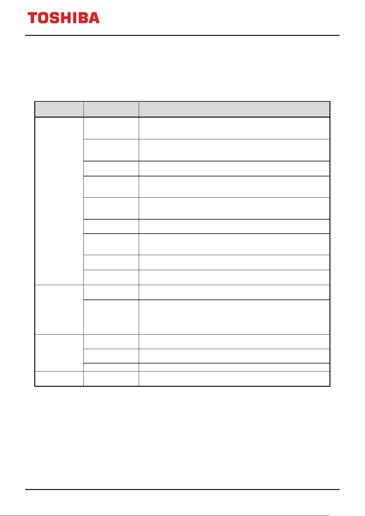
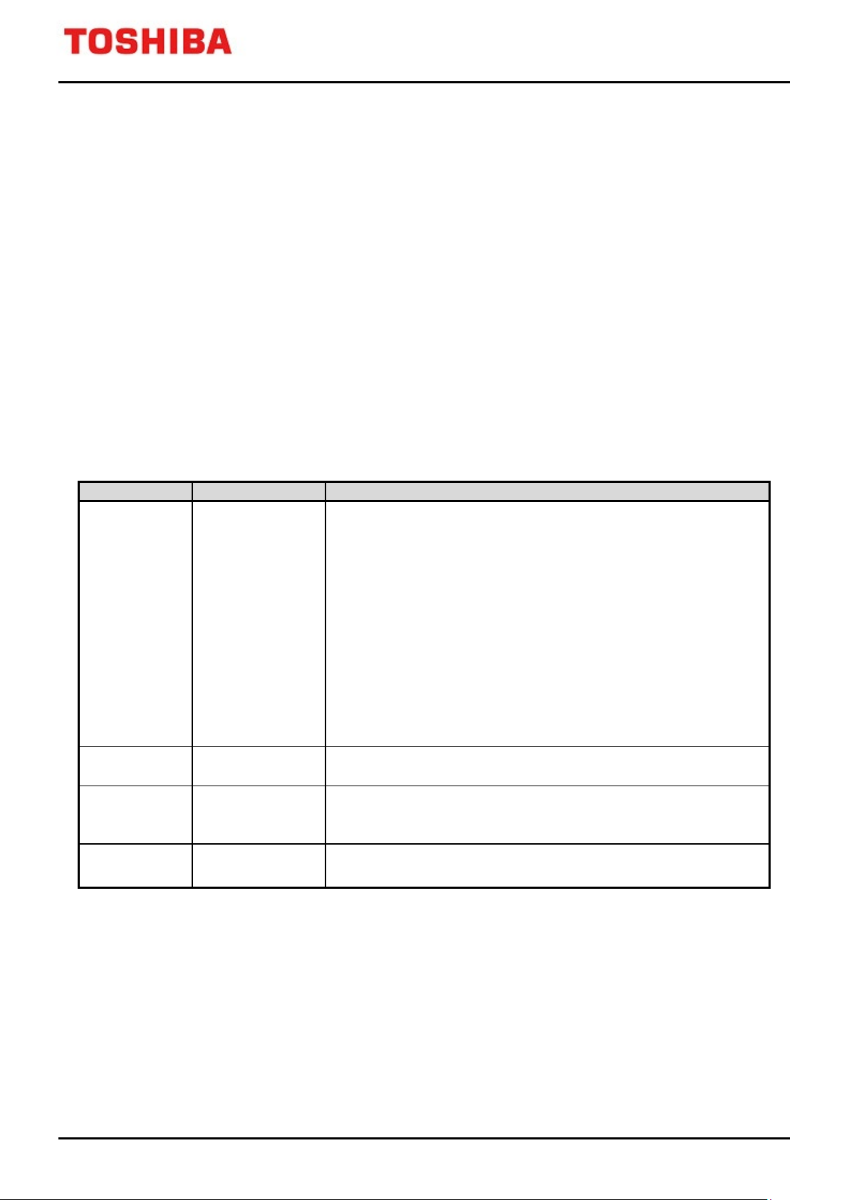
1. Outlines
The advanced vector engine plus (hereafter referred to as VE) can support vector control of 1 channel motor in 1
unit. The following is a list of functions.
Function Operation
Calculation
function
Basic function
Current control task
calculation task
Output voltage
transformation task
Output control task
Input process task
Input current
transformation task
Individual function
Scheduling control
Computation task for vector control
- Non-interference control
- Phase transformation: 2 types(Space vector transformation, Inverse
- Output limit possibility
number (2 types).
Schedule
manager
Interrupt control
Other function
Start control
Error interrupt
Output for
debugging
- Repeat start
- Start input schedule by end of AD conversion.
Start from the standby state after the output schedule ends from the input
Interrupt that occurs at the completion of schedule
Note1: For details of the PMD, refer to the reference manual "Advanced Programmable Motor Control
Circuit".
Note2: For details of the ADC, refer to the reference manual "12-bit Analog to Digital Converter".
2021-02-24
Rev. 3.1
Page 12
12 / 107
Ta sk s
Current Control
Output voltage
transformation
Output control
Trigger generation
Input process
Input current
transformation
Scheduler
Schedule 0
Schedule
management
Start co
ntrol
Schedule
control
Interrupt control
Registers
Computation
Unit
INTPWMx
INTVCNx
Decoder
Error detection
ADC
INTADxPDA
INTADxPDB
INTVCTx
VExDBGO
Schedule 1
Schedule 15
PMD
ADxREG0 to 3
VExCMPU to W
VExTRGCMP0,1
VExTRGSEL
VExEMGRS
VExOUTCR
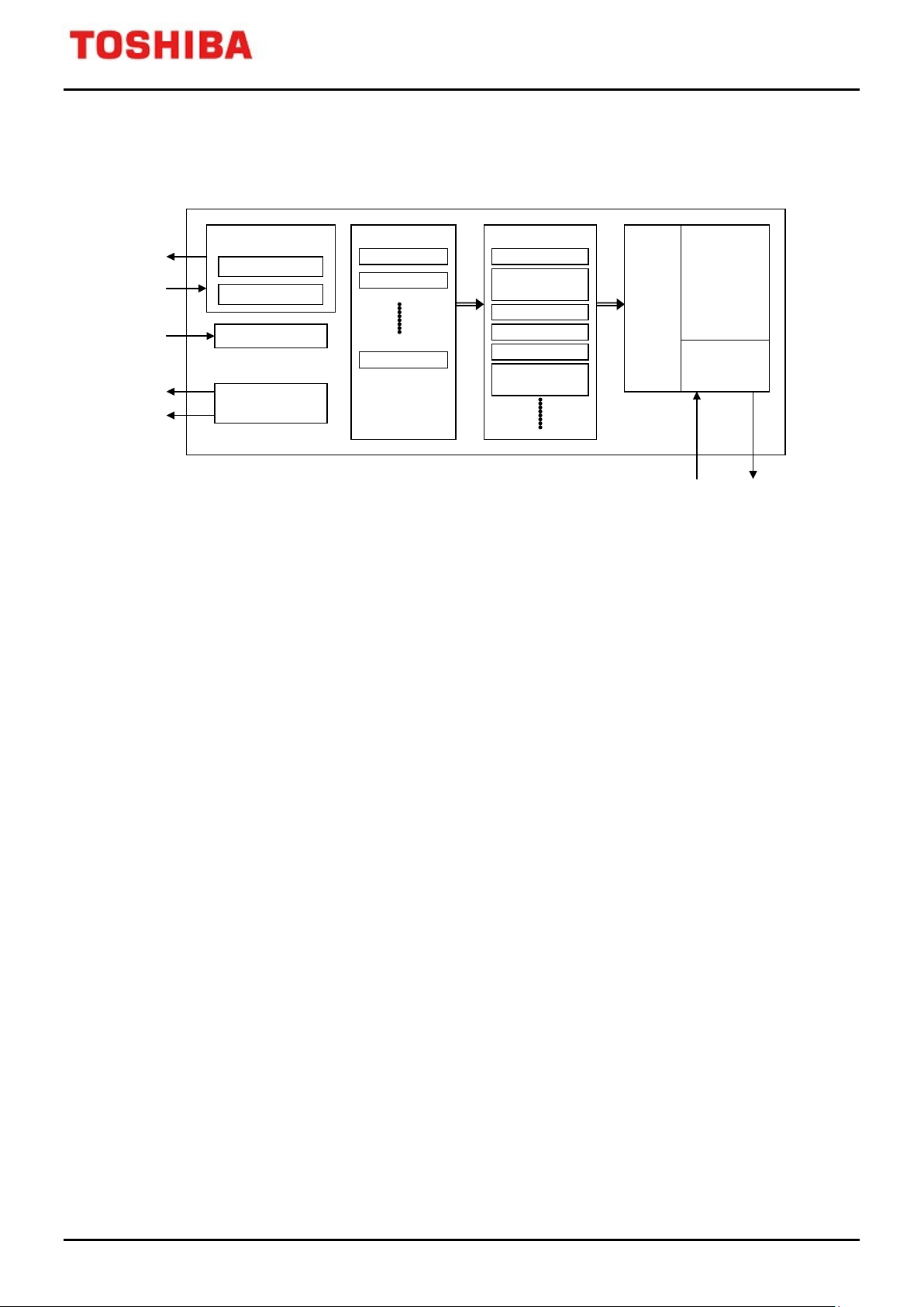
2. Configuration
2.1. Configuration of the VE
TXZ/TXZ+ Family
Advanced Vector Engine Plus
Figure 2.1 Block diagram of VE
2021-02-24
Rev. 3.1
Page 13
TXZ/TXZ+ Family
13 / 107
U-phase PWM duty
([VExCMPU] register output to PMD)
V-phase PWM duty
([VExCMPV] register output to PMD)
W-phase PWM duty
([VExCMPW] register output to PMD)
Trigger compare 0
([VExTRGCMP0] register output to PMD)
([VExTRGCMP1] register output to PMD)
Synchronous trigger output selection
([VExTRGSEL] register output to PMD)
Conduction control / output control
([VExOUTCR] register output to PMD)
EMG release
[VExEMGRS]
9
INTPW Mx
PWM interrupt (from PMD)
Input
Product Information
ADC conversion result 0
(Current 1 data from ADC)
ADC conversion result 1
(Current 2 data from ADC)
ADC conversion result 2
(Current 3 data from ADC)
ADC conversion result 3
(DC voltage data from ADC)
ADC conversion end interrupt A
(Trigger from ADC)
ADC conversion end interrupt B
(Trigger from ADC)
16
INTVCNx
Schedule end interrupt
Output
Exception, Product Information
17
INTVCTx
Task end interrupt
Output
Exception, Product Information
18
VExDBGO
Task transition signal (debug output)
Output
Product Information
Advanced Vector Engine Plus
Table 2.1 List of signals
No Signal name Signal name I/O Related Reference manual
1 VExCMPU
2 VExCMPV
3 VExCMPW
4 VExTRGCMP0
5 VExTRGCMP1
6 VExTRGSEL
7 VExOUTCR
8 VExEMGRS
10 ADxREG0
11 ADxREG1
12 ADxREG2
13 ADxREG3
Trigger compare 1
(
register output to PMD)
Output Product Information
Output Product Information
Output Product Information
Output Product Information
Output Product Information
Output Product Information
Output Product Information
Output Product Information
Input Product Information
Input Product Information
Input Product Information
Input Product Information
14 INTADxPDA
15 INTADxPDB
Input Product Information
Input Product Information
2021-02-24
Rev. 3.1
Page 14
TXZ/TXZ+ Family
14 / 107
VE ch0
PMD ch0
ADC unit A
Trigger output
Port
UO0
VO0
WO0
XO0
YO0
ZO0
・
・
・
Port
AINAx
ADAREG0
ADAREG1
ADAREG2
ADAREG3
VE0CMPU
VE0CMPV
VE0
CMPW
VE0OUTCR
VE0EMGRS
VE0TRGCMP0
VE0TRGCMP1
VE0TRGSEL
INTPW M0
INTPW M0
PMD0CMPU
PMD0CMPV
PMD0CMPW
PMD0OUTCR
PMD0EMGRS
PMD0TRGCMP0
PMD0TRGCMP1
PMD0TRGSEL
PWM output
Protect signal
(Internal)
EMG0
OVV0
Protect signal
(External)
General purpose trigger
PMD trigger 0 to 5
Monitor function output
from timer
Analog input
INTADAPDA
INTADAPDA
INTADAPDB
INTADAPDB
Current 1 input
Current 2 input
Current 3 input
DC voltage input
ADAREG0
ADAREG1
ADAREG2
ADAREG3
Advanced Vector Engine Plus
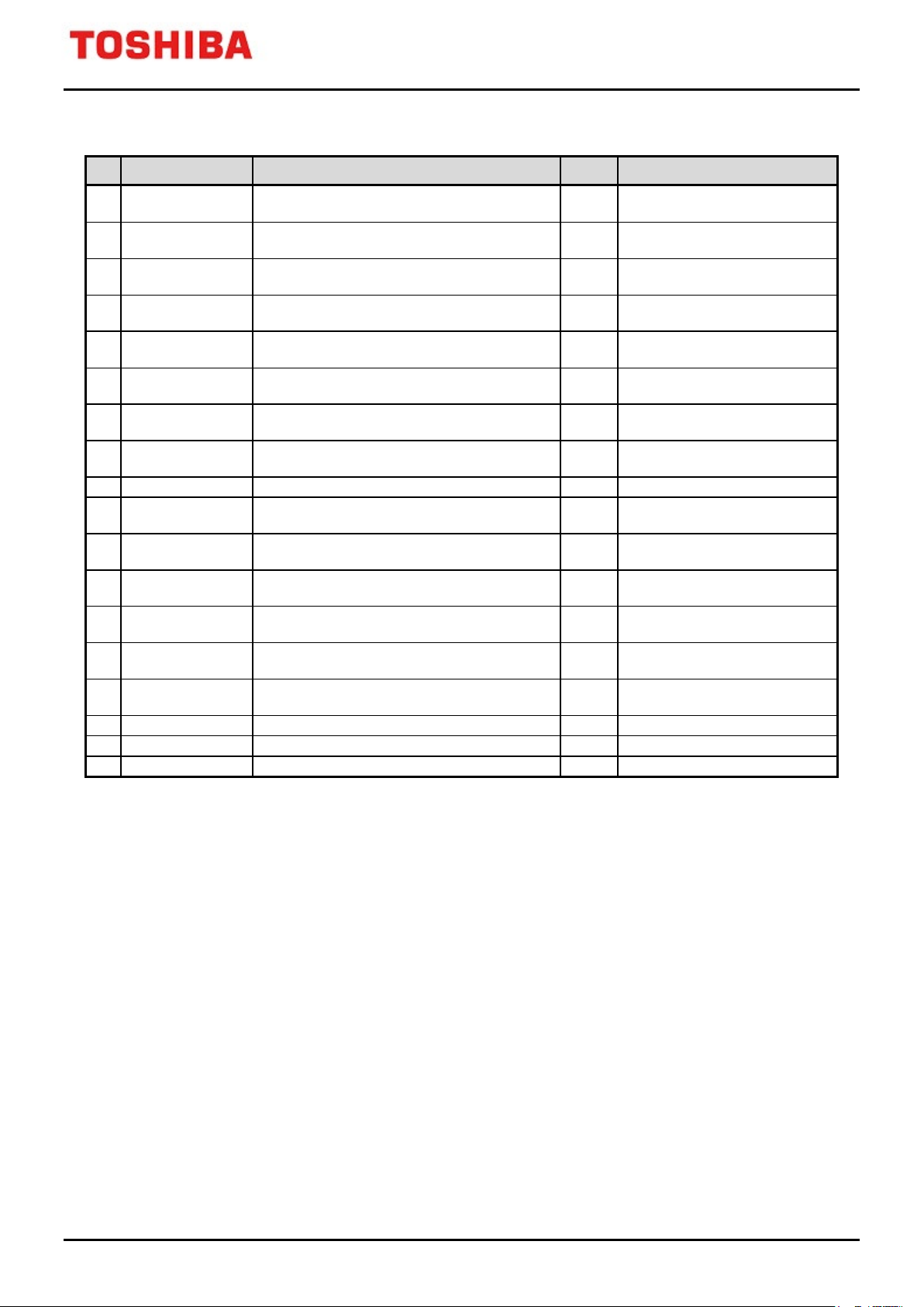
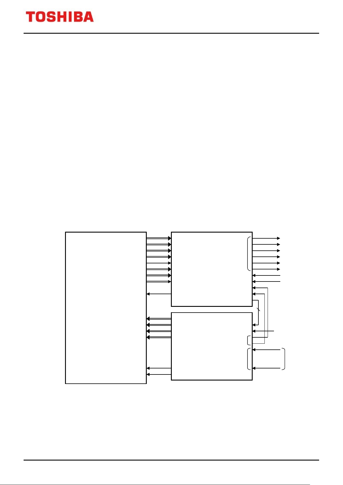
2.2. Interaction between the VE, PMD, and ADC
As shown in Figure 2.2, the VE allows to swap data between the PMD and ADC directly.
When the [PMDxCMPU], [PMDxCMPV], [PMDxCMPW], [PMDxMDOUT], [PMDxTRGCMP0],
[PMDxTRGCMP1] and [PMDxTRGSEL] registers of the PMD is set to the VE mode with the
[PMDxMODESEL] register, these registers are switched to [VExCMPU], [VExCMPV], [VExCMPW],
[VExOUTCR], [VExTRGCMP0], [VExTRGCMP1] and [VExTRGSEL] of the VE registers(Note). In this case,
these VE registers cannot be controlled via the corresponding registers of the PMD by the CPU. These registers
can be written by the VE. There are no read/write restrictions for other PMD registers.
The VE can read the value of the conversion result storage registers ([ADxREG0], [ADxREG1], [ADxREG2],
[ADxREG3]) of the ADC in the input process task. When reading the conversion result, phase information set in
the conversion program for each synchronous trigger from the PMD is also read from the ADC.
Note: Even if PMD register is switched to VE register, double buffer / triple buffer function of PMD is
valid. Refer to "Advanced Programmable Motor Control Circuit" in the reference manual for details
of buffer function.
When executing double buffers / triple buffers with PMD, while executing the task of operating
these registers with VE (output control 1 task/output control 2 task/trigger generation task, refer to
"3.3 Description of Tasks".) Even if the double buffer / triple buffer execution stage update timing is
reached, the execution stage is not updated.
Figure 2.2 Connection diagram of VE and peripherals
2021-02-24
Rev. 3.1
Page 15

TXZ/TXZ+ Family
15 / 107
RESET
Initial input
Stop
Positioning
Forced
commutation
Speed control by
current feedback
Brake
Initial setting
EMG release
:
Executed by the VE
:
Software control
Change
[VExACTSCH]
Enable VE
Change
[VExMODE]
Change [VExACTSCH
]
Change [VExMODE
]
Change [VExACTSCH]
Change [VExMODE]
Change [VExACTSCH]
Change [VExMODE]
Change [VExACTSCH]
Change [VExMODE]
Change
[VEx
ACTSCH]
Change[VExMODE]
Advanced Vector Engine Plus
3. Description of Operations
3.1. Clock Supply
When you use VE, please set an applicable clock enable bit to "1" (clock supply) in Clock supply and stop register
A for fsys ([CGFSYSENA], [CGFSYSMENA]), Clock supply and stop register B for fsys ([CGFSYSENB],
[CGFSYSMENB]), and Clock supply and stop register for fc ([CGFCEN]).
An applicable register and the bit position vary according to a product. Therefore, the register may not exist with
the product. Please refer to "Clock Control and Operation Mode" of the reference manual for the details.
3.2. Schedule Management
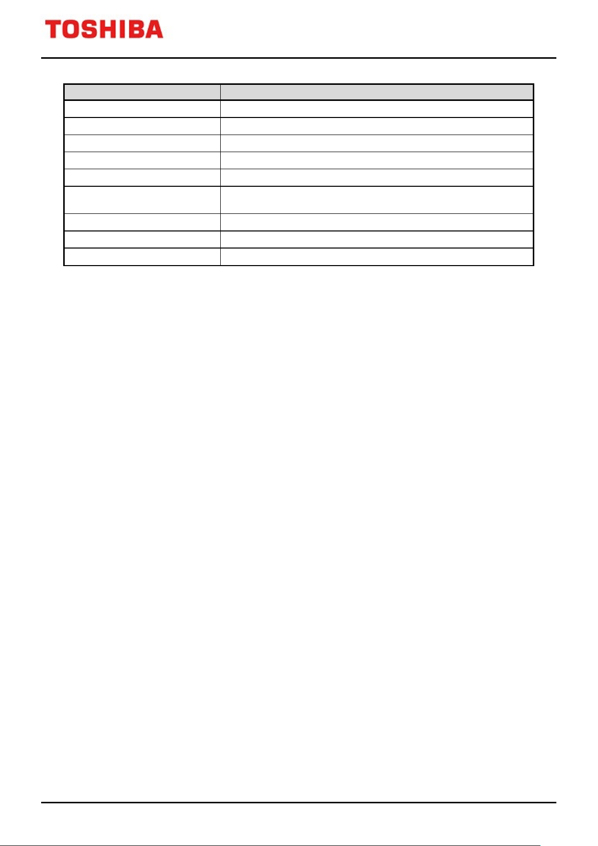
Figure 3.1 shows a flowchart of motor control. The VE changes operation status according to the schedule setting
([VExACTSCH]) and mode setting ([VExMODE]).
Figure 3.1 Example of Motor Control Operation Status Flowchart
2021-02-24
Rev. 3.1
Page 16
Advanced Vector Engine Plus
16 / 107
Item
Function
RESET Resets the MCU.
Initial setting Specifies the initial setting by software.
Stop Stops the motor.
Initial input Samples and stores zero-current data when the motor is at stop.
Positioning Controls the motor initial position.
TXZ/TXZ+ Family
Forced commutation
Speed control by current feedback Control motor rotation speed by current feedback.
Brake Deceleration control
EMG release Release the EMG protection state.
Rotates the motor. The motor is rotated without current feedback control at
a specified speed in a motor activation period.
2021-02-24
Rev. 3.1
Page 17
TXZ/TXZ+ Family
17 / 107
Provided by
execution
SIN/COS
Output
formation
for
for
mation
Input
formation
Task 5
Task 6
Task 7
Task 8
Task 11
Task 0
Task 9
Task 1
Task 2
Task 10
Task 3
Task 4
Task 12
Task 13
0:Individual
task execution
(Note 1)
(Note 1)
(Note 1)
(Note 1)
(Note 1)
(Note 1)
(Note 1)
(Note 1)
(Note 1)
(Note 1)
10: Schedule 10
11: Schedule 11
12: Schedule 12
13: Schedule 13
14: Schedule 14
Advanced Vector Engine Plus
3.2.1. Schedule Control
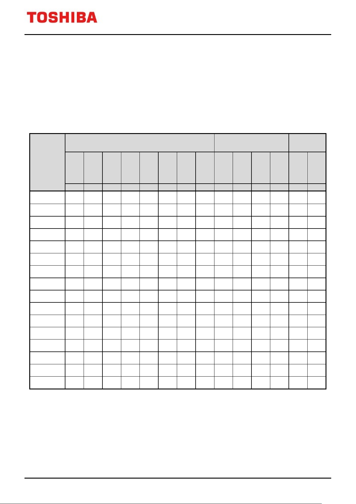
An operation schedule is selected with the [VExACTSCH] register.
The schedule is comprised of the output schedule handling output process tasks and the input schedule handling
input process tasks. Table 3.1 shows the relationship between the schedules and operation tasks.
A task operation is specified with the dedicated register according to the motor control method.
Table 3.1 Execution task in each schedule
Output schedule
execution tasks
Input schedule
execution tasks
only individual
Schedule
Selection
[VExACTSCH]
<VACT>
1: Schedule 1
Current
control
calcula-
coordi-
tion
(Note 1)
nate
axis
trans-
Output
phase
trans-
mation
1
Output
phase
trans-
mation
2
-
Output
control
1
Output
control
2
-
Trigger
genera-
tion
(Note 1)
Input
process
1
Input
process
2
-
Input
phase
trans-
for
coordi-
nate
axis
trans-
ATAN2
calcula-
tion
(Note 1) (Note 1)
- -
Square
root
calcula-
tion
2: Schedule 2 - - - - -
3: Schedule 3 - - - - -
4: Schedule 4 -
-
-
-
- -
5: Schedule 5 - - - - - -
6: Schedule 6 - - - - - -
7: Schedule 7 -
-
-
-
- -
8: Schedule 8 - - - - -
9: Schedule 9 - - - - - - - - - - -
15:Schedule 15 - - - - - - - - - -
-
- - - - - - - -
- - - - - - - - -
- - - - - - - - -
-
- - - - - - - -
- - - - - - - - - -
Note 1: Only the tasks that are specified with [VExTASKAPP] are executed.
Note 2: : Execution task, -: Non execution task
2021-02-24
Rev. 3.1
Page 18
18 / 107
Setting
Phase
<PVIEN>
Forced
commutation
Current feedback
speed control
×
Start command
Execute
output schedule
Execute
input schedule
Wait for
start trigger
Schedule end
Yes
No
Start trigger
Repeated specified
number of times?
TXZ/TXZ+ Family
Advanced Vector Engine Plus
Table 3.2 Example of setting for typical operation flow
Motor control
flow
Stop 9 0
Initial input 9 0
Positioning 1 5 0 01 0
Brake 4 6 0 01 0
EMG release 9 0
Short circuit brake 4 6
Schedule
setting
[VExACTSCH]
<VACT>
1 5 1 01 0
1 5 1 01 0
Task selection
[VExTASKAPP]
<VTASK>
interpolation
enable
[VExMODE]
×
×
×
Output control
operation
[VExMODE]
<OCRMD>
00 0
00 1
11 0
10 0
Zero-current
detection
[VExMODE]
<ZIEN>
×: don’t care
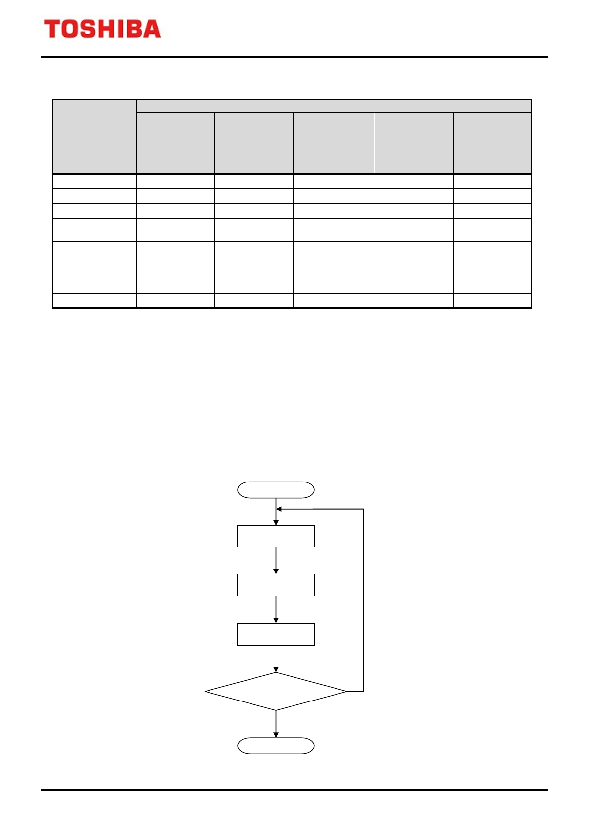
An output schedule starts operation with the command ([VExCPURUNTRG]). When all output-related tasks are
completed, the VE enters standby state and waits for a start trigger ([VExTRGMODE] setting).
An input schedule starts operation by a start trigger. When all input-related tasks are completed, the VE generates
an interrupt to the CPU and enters halt state. However, if the number of repeating of the schedule
([VExREPTIME]) is set to "2" or more, the output schedules continue execution. An interrupt does not occur
until the schedules have been executed for the specified number of times.
Note: Repeat setting is not available in Schedule 10 to Schedule 15. (The schedule ends once even if the
condition is [VExREPTIME] ≥ 2.)
Figure 3.2 Operation schedule flowchart
2021-02-24
Rev. 3.1
Page 19
TXZ/TXZ+ Family
19 / 107
Register name
Function
Advanced Vector Engine Plus
3.2.2. Start Control
Before the schedule is started, set the VE to enable ([VExEN]<VEEN> = 1), and then set the operation schedule
selection register ([VExACTSCH]), task selection register ([VExTASKAPP]) and operation schedule repeat
specify register ([VExREPTIME]). After that, the schedule can be executed as follows:
A schedule of the VE is comprised of output schedules and input schedules. Typically, the VE enters wait state
after an output schedule is complete. At this time, if a startup trigger occurs, an input schedule is executed.
The output schedule and the input schedule are started on different conditions below:
● Start conditions for the output schedule
‒ Starting by the command. A task ([VExTASKAPP]) is specified with [VExCPURUNTRG].
‒ Repeat setting. Starting after the input schedules have been executed for the number of times
([VExREPTIME] ≥ 1).
● Start conditions for the input schedule
‒ Starting an input process task that is started from wait state by a trigger (specified with
[VExTRGMODE]). In this case, the VE is in wait state after the output schedule is complete.
‒ Starting by the command. A task ([VExTASKAPP]) is specified with [VExCPURUNTRG].
[VExACTSCH]
[VExTASKAPP]
[VExREPTIME]
[VExTRGMODE]
Operation
schedule selection
Starting
task designation
The number of
repeating of
the schedule
Start trigger mode
selection
Table 3.3 Schedule-related tasks
0x0: Only the task specified with [VExTASKAPP] is executed.
0x1: Schedule 1 is executed.
0x2: Schedule 2 is executed.
0x3: Schedule 3 is executed.
0x4: Schedule 4 is executed.
0x5: Schedule 5 is executed.
0x6: Schedule 6 is executed.
0x7: Schedule 7 is executed.
0x8: Schedule 8 is executed.
0x9: Schedule 9 is executed.
0xA: Schedule 10 is executed.
0xB: Schedule 11 is executed.
0xC: Schedule 12 is executed.
0xD: Schedule 13 is executed.
0xE: Schedule 14 is executed.
0xF: Schedule 15 is executed.
Specifies the task number that can be executed among the selected
operation schedule.
Sets the number from "1" to "15".
Note: When one-time execution is specified, set "1".If "0" is set, the
schedule is not executed.
Selects the input schedule trigger.
Sets INTADxPDA or INTADxPDB.
2021-02-24
Rev. 3.1
Page 20

Advanced Vector Engine Plus
20 / 107
3.2.3. Interrupt Control
The VE has a schedule end interrupt (INTVCNx) that occurs at the completion of the schedule, and a task
completion interrupt (INTVCTx) that occurs at the completion of specified task.
● Schedule end interrupt
(1) Specifies the schedule with the operation schedule selection register ([VExACTSCH]). Sets the
command ([VExCPURUNTRG] = 1).
(2) When the schedules have been executed for the specified times ([VExREPTIME]), an INTVCNx
interrupt occurs.
(3) If the error detection interrupt control is enabled ([VExERRINTEN]<VERREN> = 1), a PWM
interrupt of the PMD circuit occurs while output schedule is being executed. Then an INTVCNx
interrupt occurs and an error flag ([VExERRDET]<VERRD>) is set to "1".
● Task end interrupt
(1) Specifies a task triggered of a task end interrupt ([VExTASKAPP]<VITASK>). Sets task end interrupt
control to enable ([VExERRINTEN]<INTTEN> = 1).
(2) Starts the schedule by the command ([VExCPURUNTRG] = 1). Sets a INTVCTx interrupt to occur at
the completion of the task specified with <VITASK>
TXZ/TXZ+ Family
2021-02-24
Rev. 3.1
Page 21
Advanced Vector Engine Plus
21 / 107
Task
number
Output coordinate
transformation
Output phase
transformation 1
Input phase
transformation
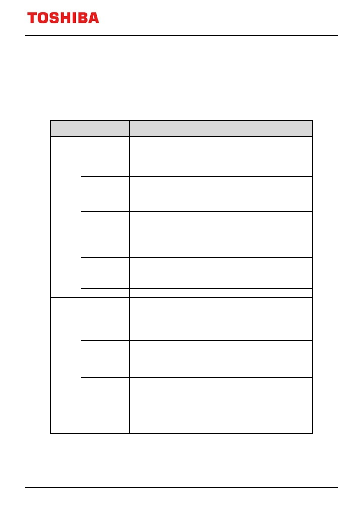
3.3. Description of Tasks
This subsection describes the outline of each task operation in the schedule.
Table 3.4 shows the task numbers that are used to specify the execution task and the start task.
Table 3.4 List of tasks
Task Task function
PI control for d-axis/q-axis (PI control output limit enable)
Current control
SIN/COS
calculation
Non-interference control for d-axis and q-axis, voltage scalar
limitation
Sine/cosine calculation
Phase interpolation (with clipping function)
TXZ/TXZ+ Family
5
6
Output
schedule
Input
schedule
axis
Output phase
transformation 2
Output control 1
Output control 2
Trigger generation
Input process 1
Input process 2
Inverse Park transformation
Transforms from 2-phase to 3-phase [SVM] 8
Transforms from 2-phase to 3-phase [Inverse Clarke
transformation]
Converts the data to PMD setting format. Switches PWM Shift
1.
Limits the PWM output.
Sets the dead time compensation control.
Converts the data to PMD setting format. Switches PWM Shift
2.
Limits the PWM output.
Sets the dead time compensation control.
Generates the synchronous trigger timing for ADC.
Corresponds to sensor, 3-shunt and 1-shunt current
detection.1-shunt is corresponded in the case of PWM Shift
prohibited or PWM Shift 1.
Captures the result of AD conversion and converts them into
fixed-point format.
Specifies the hysteresis width to determine the current polarity.
Corresponds to sensor, 3-shunt and 1-shunt current
detection.1-shunt is corresponded in the case of PWM Shift 2.
Captures the result of AD conversion and converts them into
fixed-point format.
Specifies the hysteresis width to determine the current polarity.
11
10
7
0
9
1
2
Transforms from 3-phase to 2-phase.
Input coordinate
axis
transformation
ATAN2 calculation Calculates the arctangent. 12
SQRT calculation Calculates the square root. 13
Performs Park transformation
Calculates the declination angle of the current vector or the
induced voltage vector on the d-q coordinate.
3
4
2021-02-24
Rev. 3.1
Page 22
22 / 107
Input process
Output control
Phase
transformation
Current control
SIN/COS
calculation
Phase
interpolation
PI
control
PI
control
Cordinate axis
transformation
[I-Park]
Phase
transformation 1
[SVM]
Output
control 1
sin,cos
VD
VQ
Valpha
Vbeta
DUTYA
DUTYB
DUTYC
SECTOR
θ
ω
Trigger
generation
Phase
transformation
[Clark]
Input
process1
Ialpha
Ibeta
VDC,VDCL
ID
IQ
PWM output
setting (PMD)
Synchronous
trigger t setting
(PMD)
Current/Voltage
detection value
(ADC)
SIN
COS
IDREF
ID
IQ
IQREF
VDC
IA
IB
IC
Phase
transformation 2
[I-Clark]
Output
control 2
Input
process2
VDC
Cordinate axis
transformation
[Park]
TXZ/TXZ+ Family
Advanced Vector Engine Plus
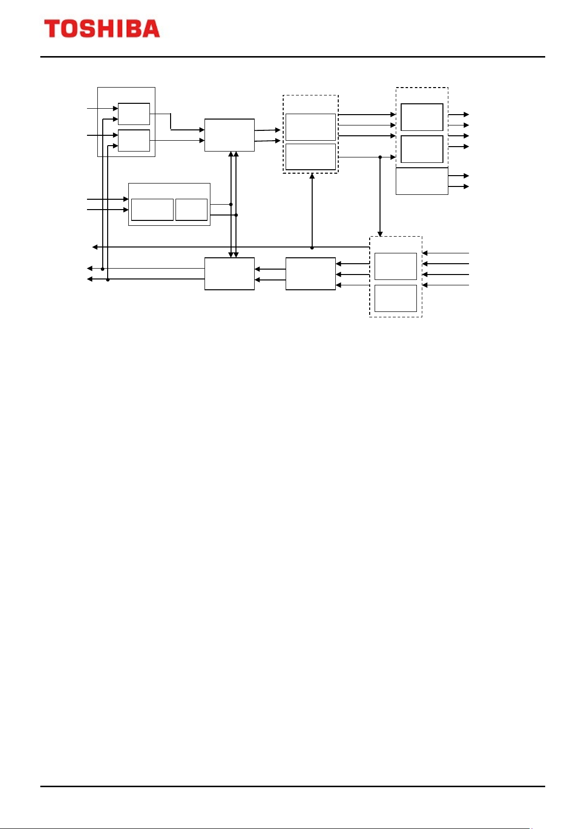
Figure 3.3 Relationship diagram of tasks
2021-02-24
Rev. 3.1
Page 23

TXZ/TXZ+ Family
23 / 107
Advanced Vector Engine Plus
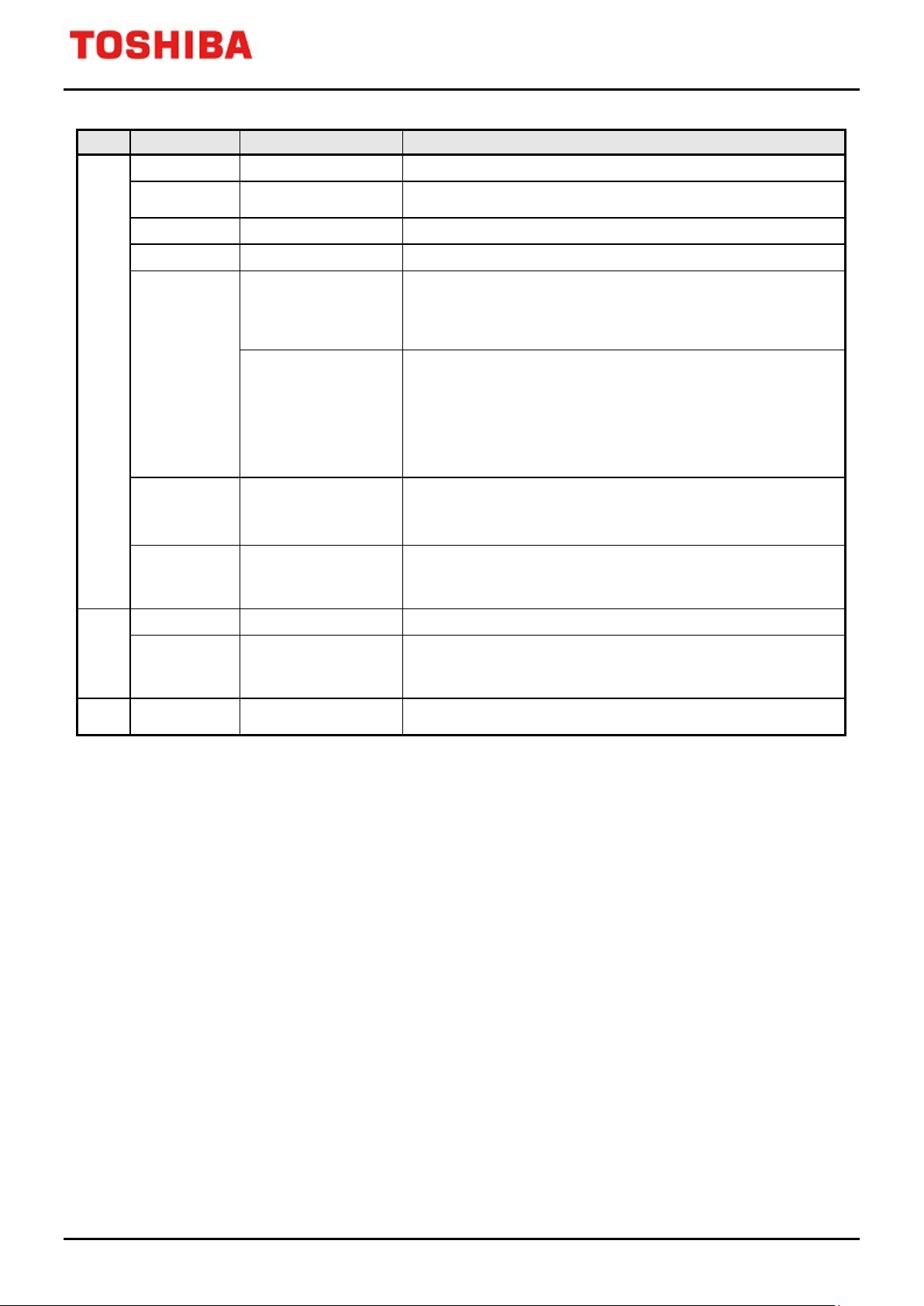
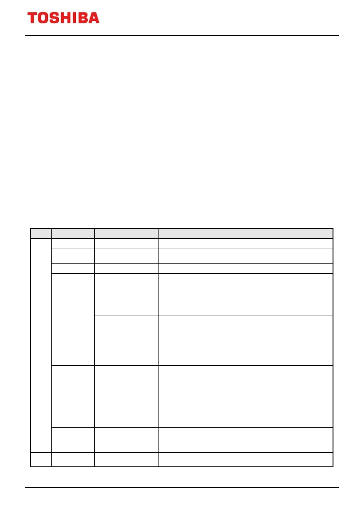
3.3.1. Current Control (Task 5)
The current control task is comprised of a PI control unit for d-axis current and a PI control unit for q-axis current,
and calculates the d-axis and q-axis voltages respectively.
The expansion control enables the non-interference control and the voltage scalar limitation that controls d-axis
and q-axis together.
a. d-axis current PI control
<Equation>
[PI control]
Δid = [VExIDREF] - [VExID] ; Calculates between the current reference value
and the current feedback
kpg = ([VExCIDKG]<CIDKPG> setting) ; Range of proportional coefficient
kig = ([VExCIDKG]<CIDKIG> setting) ; Range of Integral coefficient
limit = [VExPIOLIM]
if (kpg ≥ 2) n = kpg ; Selected range is more than twice
Save Range of proportional coefficient
limit = limit / kpg ; Limit correction
kig = kig / kpg ; Range correction of integral
kpg = 1 ; Range correction of proportional
else n = 1
cidkp = [VExCIDKP] × kpg ; Proportional coefficient
cidki = [VExCIDKI] × kig ; Integral coefficient
vdi0 = cidki × Δid + VDI ; Calculates the integral components.
vd0 = cidkp × Δid + vdi0 ; Calculates the voltage by adding the
proportional components.
[PI control output limitation]
if (vd0 > limit) ; The upper-limit value
vd = limit
[VExMCTLF]<PIDOVF> = 1
else if (vd0 < -limit) ; The lower-limit value
vd = -limit
[VExMCTLF]<PIDOVF> = 1
else
[VExVD] = vd × n ; Save more than a double proportional range
to be compensated.
[Anti-windup]
Δvd = vd - vd0 ; Calculates the difference between the d-axis
voltage and the limit.
VDI = vdi0 + Δvd × ([VExMODE]<AWUMD> setting) ; Reflects the above difference
to the integral component.
vd = vd0
2021-02-24
Rev. 3.1
Page 24
24 / 107
Register name
Function
Detail
d-axis current reference
value
Integral component
of d-axis voltage
TXZ/TXZ+ Family
Advanced Vector Engine Plus
Input
[VExID]
[VExIDREF]
[VExCIDKP]
[VExCIDKI]
[VExCIDKG]
[VExPIOLIM]
[VExMODE]
d-axis current
Proportional coefficient
Integral coefficient
[3:0] Sets a range of
d-axis PI control integral
coefficient
[11:8] Sets a range of
d-axis PI control
proportional coefficient
PI control output
limitation
[9:8] Anti-windup ratio
setting when output is
limited.
32-bit fixed-point data (31 fractional bits)
16-bit fixed-point data(15 fractional bits)
16-bit data
16-bit data
<CIDKIG> Range of Integral coefficient
0000: 1 / 1 0001: 1 / 2
0011: 1 / 2
0101 to 1111: Reserved
<CIDKPG> Range of proportional coefficient
0000: 1 / 1 0001: 1 / 2
0011: 1 / 2
0101 to 1000: Reserved
1001: 2 1010: 2
1100: 2
1101 to 1111: Reserved
16-bit fixed-point data (15 fractional bits)
Valid range: 0x0000 to 0x7FFF
Output limitation is disabled when [VExPIOLIM] = 0x0000.
<AWUMD>
00: Disabled 01: 1 / 4 10: 1 / 2
11: 1 / 1
12
12
4
0100: 1 / 2
0100: 1 / 2
4
16
4
16
2
0010: 1 / 2
0010: 1 / 2
1011: 2
8
8
3
Output
Internal
Note: The VDI is comprised of 64 bits. The upper is used for the [VExVDIH] register and the lower is used for
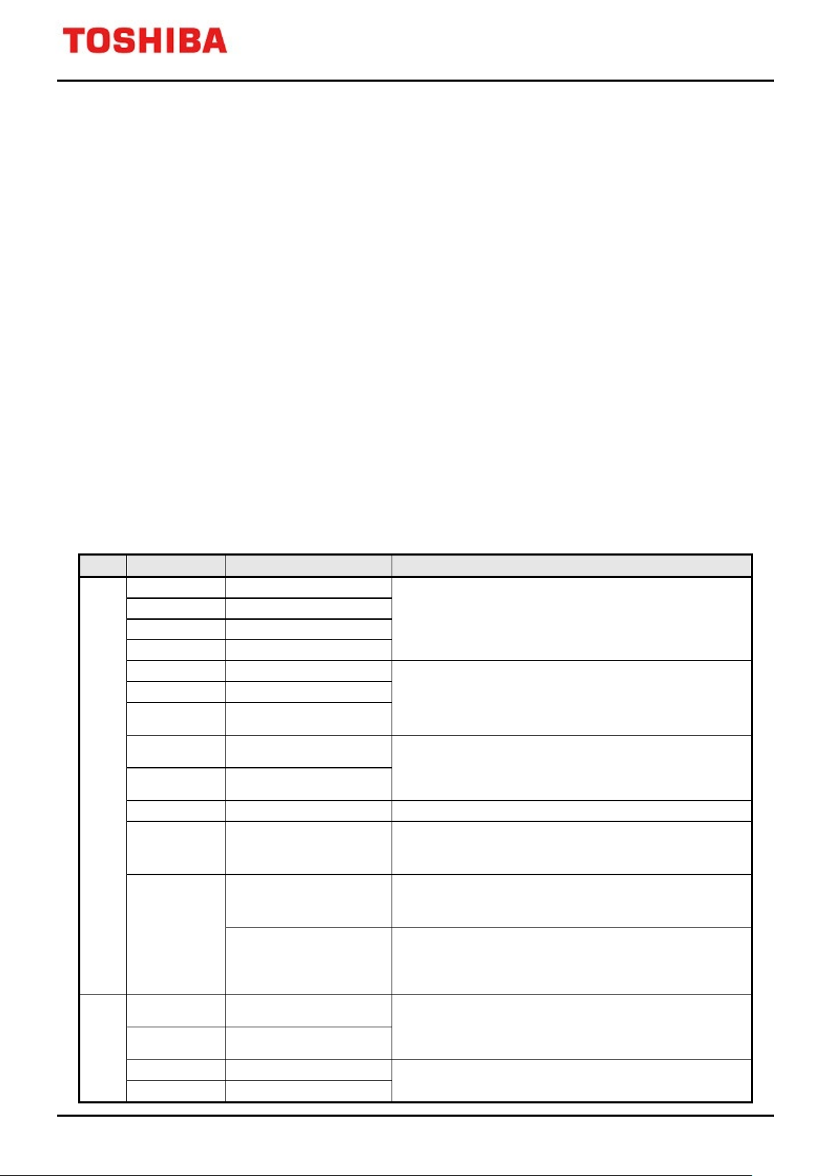
b. q-axis current PI control
<Equation>
[PI control]
Δiq = [VExIQREF] - [VExIQ] ; Calculates between the current reference value
and the current feedback
kpg = ([VExCIQKG]<CIQKPG> setting) ; Range of proportional coefficient
kig = ([VExCIQKG]<CIQKIG> setting) ; Range of Integral coefficient
limit = [VExPIOLIM]
if (kpg ≥ 2) n = kpg ; Selected range is more than twice,
Save Range of proportional coefficient
limit = limit / kpg ; Limit correction
kig = kig / kpg ; Range correction of integral
kpg = 1 ; Range correction of proportional
else n = 1
ciqkp = [VExCIQKP] × kpg ; Proportional coefficient
ciqki = [VExCIQKI] × kig ; Integral coefficient
vqi0 = ciqki × Δiq + VQI ; Calculates the integral components.
[VExVD]
[VExMCTLF]
VDI
d-axis voltage
[8] Flag for d-axis output
limitation on PI control
the [VExVDILH] register
32-bit fixed-point data (31 fractional bits)
<PIDOVF>
0: |d-axis output on PI control | ≤ [VExPIOLIM]
1: |d-axis output on PI control | > [VExPIOLIM]
64-bit fixed-point data (63 fractional bits)
2021-02-24
Rev. 3.1
Page 25
TXZ/TXZ+ Family
25 / 107
Register name
Function
Detail
q-axis current reference
value
Integral component
of q-axis voltage
Advanced Vector Engine Plus
vq0 = ciqkp × Δiq + vqi0 ; Calculates the voltage by adding the
proportional components.
[PI control output limitation]
if (vq0 > limit) ; The upper-limit value
vq = limit
[VExMCTLF]<PIQOVF> = 1
else if (vq0 < -limit) ; The lower-limit value
vq = -limit
[VExMCTLF]<PIQOVF> = 1
else vq = vq0
[VExVQ] = vq × n ; Save more than a doubled proportional range
to be compensated.
[Anti-windup]
Δvq = vq - vq0 ; Calculates the difference between the q-axis
voltage and the limit.
VQI = vqi0 + Δvq × ([VExMODE]<AWUMD> setting) ; Reflects the above difference to the
integral component.
Input
[VExIQ]
[VExIQREF]
[VExCIQKP]
[VExCIQKI]
[VExCIQKG]
[VExPIOLIM]
[VExMODE]
q-axis current
Proportional coefficient
Integral coefficient 16-bit data
[3:0] Sets a range of
q-axis PI control integral
coefficient
[11:8] Sets a range of
q-axis PI control
proportional coefficient
PI control output
limitation
[9:8] Anti-windup ratio
setting when output is
limited.
32-bit fixed-point data (31 fractional bits)
16-bit fixed-point data(15 fractional bits)
16-bit data
<CIQKIG> Range of Integral coefficient
0000: 1 / 1 0001: 1 / 2
0011: 1 / 2
0101 to 1111: Reserved
<CIQKPG> Range of proportional coefficient
0000: 1 / 1 0001: 1 / 2
0011: 1 / 212 0100: 1 / 216
0101 to 1000: Reserved
1001: 2 1010: 2
1100: 24
1101 to 1111: Reserved
16-bit fixed-point data (15 fractional bits)
Valid range: 0x0000 to 0x7FFF
Output limitation is disabled when [VExPIOLIM] = 0x0000.
<AWUMD>
00: Disabled 01: 1 / 4 10: 1 / 2
11: 1
12
4
0100: 1 / 216
4
2
1011: 2
0010: 1 / 2
0010: 1 / 2
3
8
8
Output
Internal
Note: The VQI is comprised of 64 bits. The upper is used for the [VExVQIH] register and the lower is used for
[VExVQ]
[VExMCTLF]
VQI
q-axis voltage
[9] Flag for q-axis output
limitation on PI control
32-bit fixed-point data (31 fractional bits)
<PIQOVF>
0: |q-axis output on PI control | ≤ [VExPIOLIM]
1: |q-axis output on PI control | > [VExPIOLIM]
64-bit fixed-point data (63 fractional bits)
the [VExVQILH] register
2021-02-24
Rev. 3.1
Page 26
TXZ/TXZ+ Family
26 / 107
Register name
Function
Detail
[VExVD]
d-axis voltage
[VExID]
d-axis current
[VExIQ]
[VExCLD]
[VExCLQ]
Motor Interlinkage magnetic
flux
Motor Inductance range
setting
Motor Interlinkage magnetic
flux range setting
[VExIDREF], [VExIQREF]
1: Expansion control is enabled.
Non-interference correction
voltage for d-axis
Non-interference correction
voltage for q-axis
[VExVD]
[VExVQ]
Advanced Vector Engine Plus
c. Non-interference control
The result of PI control is corrected using the results of the interference to d-axis and q-axis based on motor
voltage equation.
<Equation>
if ([VExMODE]<T5ECEN> = 1) ; Expansion control is enabled
ld = [VExCLD] × ([VExCLG] setting) ; d-axis inductance
lq = [VExCLQ] × ([VExCLG] setting) ; q-axis inductance
phi = [VExCPHI] × ([VExCPHIG] setting) ; Interlinkage magnetic flux
id = [VExID] ; Feedback current
iq = [VExIQ]
if ([VExFMODE]<IDQSEL> = 1) id = [VExIDREF] ; Inputs a command value
iq = [VExIQREF]
[VExVDE] = - [VExOMEGA] × iq × lq ; Calculates the interference to d-axis
[VExVQE] = [VExOMEGA] × id × ld + [VExOMEGA] × phi ; Calculates the interference to q-axis
if ([VExMODE]<NICEN> = 1) ; Non-interference control is enabled
[VExVD] = [VExVD] + [VExVDE]
[VExVQ] = [VExVQ] + [VExVQE]
Input
Output
[VExVQ]
[VExCPHI]
[VExCLG]
[VExCPHIG]
[VExOMEGA]
[VExFMODE]
[VExMODE]
[VExVDE]
[VExVQE]
q-axis voltage
q-axis current
Motor d-axis inductance
Motor q-axis inductance
Rotational speed 16-bit fixed-point data (15 fractional bits)
[4] Selects Non-interference
control input
[11] Non-interference control
enable
[10] Expansion control
enable
d-axis voltage
q-axis voltage
32-bit fixed-point data (31 fractional bits)
16-bit fixed-point data (11 fractional bits)
000: 1 / 1 001: 1 / 24 010: 1 / 28
011: 1 / 2
101 to 111: Reserved
<IDQSEL>
0: Use [VExID], [VExIQ]
1: Use
<NICEN>
0: Non-interference control is disabled.
1: Non-interference control is enabled.
<T5ECEN>
0: Expansion control is disabled.
(Non-interference control is disabled.)
16-bit fixed-point data (15 fractional bits)
32-bit fixed-point data (31 fractional bits)
12
100: 1 / 216
2021-02-24
Rev. 3.1
Page 27

TXZ/TXZ+ Family
27 / 107
Advanced Vector Engine Plus
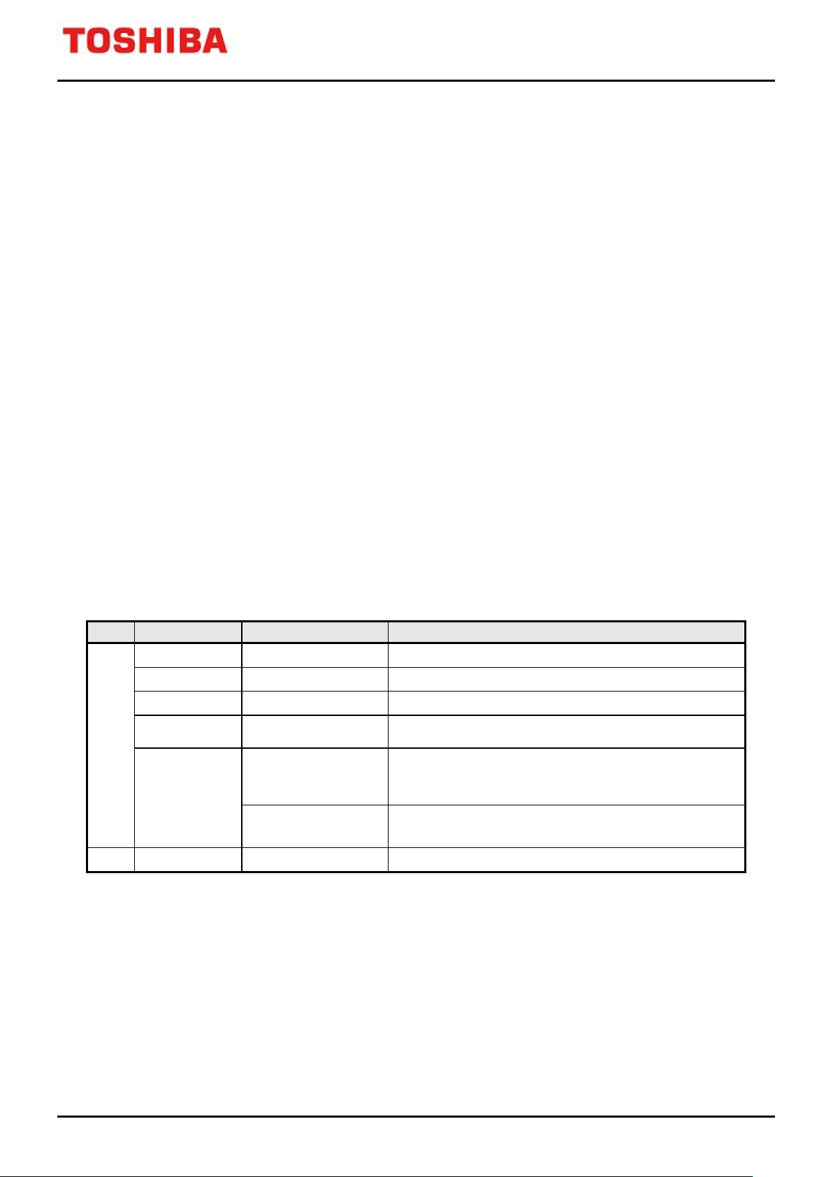
d. Voltage scalar limitation
The voltage scalar limitation controls d-axis voltage and q-axis voltage, so as to be lower the composite value (the
2
square root of VD
+ VQ2) that is comprised of d-axis voltage and q-axis voltage than the limit value.
<Equation>
if ([VExMODE]<T5ECEN> = 1) ; Expansion control is enabled.
[VDQ calculation]
if (([VExVD]
2
+ [VExVQ]2)> [VExVSLIM]2) ; Confirm the excess
if ([VExFMODE]<VSLIMMD> = 00) ; Voltage scalar limitation is disabled
[VExVDQ] = SQRT([VExVD]
2
+ [VExVQ]2)
else if ([VExFMODE]<VSLIMMD> = 01) ; Scalar limitation on the d-axis direction
2
[VExVDQ] = SQRT([VExVSLIM]
+ [VExVQ]2)
else if ([VExFMODE]<VSLIMMD> = 10) ; Scalar limitation on the q-axis direction
[VExVDQ] = SQRT([VExVSLIM]
2
+ [VExVD]2)
else if ([VExFMODE]<VSLIMMD> = 11) ; dq proportional scalar limitation
[VExVDQ] = SQRT([VExVD]
else [VExVDQ] = SQRT([VExVD]
2
+ [VExVQ]2)
2
+ [VExVQ]2) ; Calculation of voltage scalar value
Note: SQRT is the square root calculation
[Calculation for the declination angle]
x = |[VExVQ]|
y = |[VExVD]|
[VExVDELTA] = ATAN(x, y)
Note: ATAN is arctangent calculation
[Limitation calculation for each axis]
if ([VExFMODE]<VSLIMMD> = 00) ; Voltage scalar limitation is disabled
vdlim = [VExVSLIM]
vqlim = [VExVSLIM]
else if ([VExFMODE]<VSLIMMD> = 01) ; Scalar limitation on the d-axis direction
vdlim = [VExVDQ]
vqlim = [VExVSLIM]
else if ([VExFMODE]<VSLIMMD> = 10) ; Scalar limitation on the q-axis direction
vdlim = [VExVSLIM]
vqlim = [VExVDQ]
else if ([VExFMODE]<VSLIMMD> = 11) ; dq proportional scalar limitation
vdlim = [VExVSLIM] × SIN([VExVDELTA])
vqlim = [VExVSLIM] × COS([VExVDELTA])
[Limitation process]
if ([VExVD] > vdlim)
[VExVD] = vdlim ; Process for the upper-limit of d-axis
[VExMCTLF]<VSOVF> = 1
else if ([VExVD] < -vdlim)
[VExVD] = -vdlim ; Process for the lower-limit of d-axis
2021-02-24
Rev. 3.1
Page 28

TXZ/TXZ+ Family
28 / 107
Register name
Function
Detail
The value of d-axis
voltage correction
The value of q-axis
voltage correction
The value of voltage
axis direction limitation.
[10] Indicates the
scalar limitation.
Advanced Vector Engine Plus
[VExMCTLF]<VSOVF> = 1
if ([VExVQ] > vqlim)
[VExVQ] = vqlim ; Process for the upper-limit of q-axis
[VExMCTLF]<VSOVF> = 1
else if ([VExVQ] < -vqlim)
[VExVQ] = -vqlim ; Process for the lower-limit of q-axis
[VExMCTLF]<VSOVF> = 1
[Correction process]
[VExVD] = [VExVD] + [VExVDCRC] ; d-axis correction
[VExVQ] = [VExVQ] + [VExVQCRC] ; q-axis correction
Input
[VExVD]
[VExVQ]
[VExVSLIM]
[VExVDCRC]
[VExVQCRC]
[VExMODE]
[VExFMODE]
[VExVDQ]
d-axis voltage
q-axis voltage
The limit value of
voltage scalar
[10] Expansion control
enable
[11:10] Limitation mode
setting
scalar or the value of
32-bit fixed-point data (31 fractional bits)
16-bit fixed-point data (15 fractional bits)
0x0000 to 0x7FFF
Limitation is disabled when [VExVSLIM] = 0x0000
16-bit fixed-point data (15 fractional bits)
<T5ECEN>
0: Expansion control is disabled.(Scalar limitation is
disabled.)
1: Expansion control is enabled.
<VSLIMMD>
00: Scalar limitation is disabled.
(Limitation in each axis is enabled.)
01: Scalar limitation is enabled.
(Limitation on the d-axis direction.)
10: Scalar limitation is enabled.
(Limitation on the q-axis direction.)
11: Scalar limitation is enabled.
(dq proportional limitation.)
16-bit fixed-point data (15 fractional bits)
Output
[VExVDELTA]
[VExVD]
[VExVQ]
[VExMCTLF]
The voltage declination
angle
d-axis voltage
q-axis voltage
excess flag for voltage
16-bit data
0x0000 to 0x4000 (0-degree to 90-degree)
32-bit fixed-point data (31 fractional bits)
<VSOVF>
0:non excess 1:excess
2021-02-24
Rev. 3.1
Page 29
TXZ/TXZ+ Family
29 / 107
Register name
Function
Detail
The value of clipped
phase
Advanced Vector Engine Plus
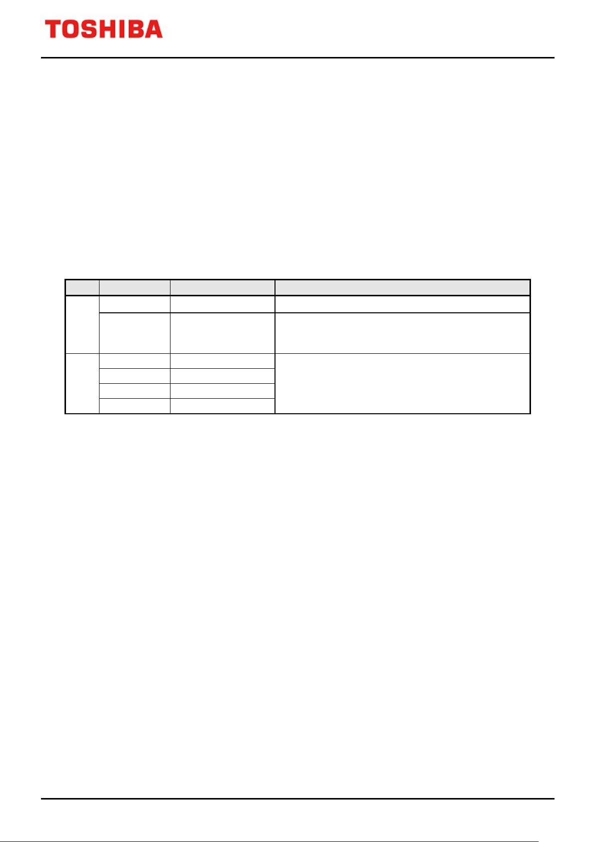
3.3.2. SIN/COS calculation (Task 6)
The SIN/COS calculation task executes phase interpolation calculation and SIN/COS calculation.
Phase interpolation calculates the rotation speed by integrating with the PWM period. It is executed only when
phase interpolation is enabled ([VExMODE]<PVIEN> = 1).
a. Phase interpolation
<Equation>
theta0 = [VExOMEGA] × [VExTPWM] + [VExTHETA] ; Calculates the value of
phase interpolation
theta0 = theta0 & 0x0000FFFF
if ([VExMODE]<CLPEN> = 1) ; Enables the clipping
if ([VExOMEGA] ≥ 0) ; On positive rotation
if ([VExTHETA] ≤ [VExTHTCLP] ≤ theta0) theta0 = [VExTHTCLP]
else if (theta0 ≤ [VExTHETA] ≤ [VExTHTCLP]) theta0 = [VExTHTCLP]
else if ([VExTHTCLP] ≤ theta0 ≤ [VExTHETA]) theta0 = [VExTHTCLP]
else if ([VExOMEGA] < 0) ; On inverse rotation
if (theta0 ≤ [VExTHTCLP] ≤ [VExTHETA]) theta0 = [VExTHTCLP]
else if ([VExTHTCLP] ≤ [VExTHETA] ≤ theta0) theta0 = [VExTHTCLP]
else if ([VExTHETA] ≤ theta0 ≤ [VExTHTCLP]) theta0 = [VExTHTCLP]
if ([VExMODE]<PVIEN> = 1) [VExTHETA] = theta0 ; Updates the [VExTHETA] value when
phase interpolation is enabled
Input
Output
[VExTHETA]
[VExOMEGA]
[VExTPWM]
[VExTHTCLP]
[VExMODE]
[VExTHETA]
Phase θ 16-bit fixed-point data (0.0 to 1.0, 16 fractional bits)
Rotational speed
PWM period rate
[0] Phase interpolation
enable
[7] Phase clipping
control
Phase θ
16-bit fixed-point data (-1.0 to 1.0, 15 fractional bits)
16-bit data
16-bit fixed-point data (0.0 to 1.0, 16 fractional bits)
<PVIEN>
0: Phase interpolation is disabled
1: Phase interpolation is enabled
<CLPEN>
0: Clipping is disabled 1: Clipping is enabled
16-bit fixed-point data (0.0 to 1.0, 16 fractional bits)
2021-02-24
Rev. 3.1
Page 30
TXZ/TXZ+ Family
30 / 107
Register name
Function
Detail
Advanced Vector Engine Plus
b. SIN/COS calculation
<Equation>
[VExSINM] = [VExSIN] ; Stores the previous value (for input process)
[VExCOSM] = [VExCOS]
[VExSIN] = SIN ([VExTHETA]) ; Calculates the SIN and COS values
[VExCOS] = SIN ([VExTHETA] + 1 / 4)
if ([VExFMODE]<MREGDIS> = 1) ; Confirms that the previous value is not maintained
[VExSINM] = [VExSIN]
[VExCOSM] = [VExCOS]
Note: SIN: Sine calculation
Input
Output
[VExTHETA]
[VExFMODE]
[VExSIN]
[VExCOS]
[VExSINM]
[VExCOSM]
Phase θ
[9] Selects to store the
previous value of SIN
and COS
The sine value of θ
The cosine value of θ
Previous sine value
Previous cosine value
16-bit fixed-point data (0.0 to 1.0, 16 fractional bits)
<MREGDIS>
0: Previous value is maintained.
1: Previous value is not maintained.
16-bit fixed-point data (-1.0 to 1.0, 15 fractional bits)
2021-02-24
Rev. 3.1
Page 31
TXZ/TXZ+ Family
31 / 107
[VExVD]
d-axis voltage
[VExVQ]
[VExSIN]
[VExCOS]
[VExVALPHA]
[VExVBETA]
Advanced Vector Engine Plus
3.3.3. Output Voltage Transformation (Coordinate Axis Transformation/Phase Transformation)
Output voltage transformation is performed in two steps: coordinate axis transformation and phase transformation.
There are two types of phase transformation: Space vector transformation and inverse Clarke transformation.
3.3.3.1. Output coordinate axis transformation (Task 7)
In the output coordinate axis task, α-axis and β-axis voltages are calculated based on d-axis voltage, q-axis voltage,
sinθ and cosθ.
<Equation>
[VExVALPHA] = [VExCOS] × [VExVD] - [VExSIN] × [VExVQ] ; Calculates Vα
[VExVBETA] = [VExSIN] × [VExVD] + [VExCOS] × [VExVQ] ; Calculates Vβ
Register name Function Detail
32-bit fixed-point data (-1.0 to 1.0, 31 fractional bits)
16-bit fixed-point data (-1.0 to 1.0, 15 fractional bits)
32-bit fixed-point data (-1.0 to 1.0, 31 fractional bits)
Input
Output
q-axis voltage
The sine value of θ
The cosine value of θ
α-axis voltage
β-axis voltage
2021-02-24
Rev. 3.1
Page 32
TXZ/TXZ+ Family
32 / 107
[VExVALPHA]
[VExVBETA]
Advanced Vector Engine Plus
3.3.3.2. Output phase transformation 1 (Space vector transformation) (Task 8)
Output phase transformation 1 determines a sector using α-axis voltage and β-axis voltage. This task calculates the
duties of a-phase voltage, b-phase voltage, and c-phase voltage based on space vector transformation in each
sector.
This task can be selected either from 2-phase or 3-phase modulation as a modulation type.
a. Sector determination
<Equation>
[VExSECTORM] = [VExSECTOR] ; Stores the previous value
valpha = [VExVALPHA]
vbeta = [VExVBETA]
if (valpha ≥ 0 & vbeta ≥ 0)
if (|valpha| ≥ |vbeta| × √(1 / 3))
if (|valpha| × √(1 / 3) ≥ |vbeta|) [VExSECTOR] = 0
else [VExSECTOR] = 1
else [VExSECTOR] = 2
else if (valpha < 0 & vbeta ≥ 0)
if (|valpha| < |vbeta| × √(1 / 3)) [VExSECTOR] = 3
if (|valpha| × √(1 / 3) < |vbeta|) [VExSECTOR] = 4
else [VExSECTOR] = 5
else if (valpha < 0 & vbeta < 0)
if (|valpha| ≥ |vbeta| × √(1 / 3))
if (|valpha| × √(1 / 3) ≥ |vbeta|) [VExSECTOR] = 6
else [VExSECTOR] = 7
else [VExSECTOR] = 8
else if (valpha ≥ 0 & vbeta < 0)
if (|valpha| < |vbeta| × √(1 / 3)) [VExSECTOR] = 9
else if (|valpha| × √(1 / 3) < |vbeta|) [VExSECTOR] = 10
else [VExSECTOR] = 11
if ([VExFMODE]<MREGDIS> = 1) [VExSECTORM] = [VExSECTOR] ; Confirm that the previous
value is disabled
Register name Function Detail
Input
Output
α-axis voltage
β-axis voltage
[9] Selects to store the
[VExFMODE]
[VExSECTOR]
[VExSECTORM] Previous [VExSECTOR]
previous value of
SECTOR
Sector information
32-bit fixed-point data (-1.0 to 1.0, 31 fractional bits)
<MREGDIS>
0: Previous sector value is maintained.
1: Previous sector value is not maintained.
4-bit data
2021-02-24
Rev. 3.1
Page 33
TXZ/TXZ+ Family
33 / 107
Register name
Function
Detail
[13] Phase
setting
[VExVDUTYA]
[VExVDUTYB]
[VExVDUTYC]
[VExTMPREG5]
Advanced Vector Engine Plus
b. Space vector transformation
(This example describes only the case where 3-phase modulation is used and [VExSECTOR] = 0, 1.)
<Equation>
kc = √3 ; Relative transformation
if ([VExFMODE]<CCVMD> = 1) kc = √2 ; Absolute transformation
if ([VExSECTOR] = 0, 1)
t1 = kc /[VExVDC] × (√3 / 2 × [VExVALPHA] -1 / 2 × [VExVBETA]) ; Calculates the t1 period.
t2 = kc /[VExVDC] × [VExVBETA]) ; Calculates the t2 period.
t3 = 1 -t1 -t2 ; Calculates the zero-vector period
if ([VExFMODE]<C2PEN> = 0) ; 3-phase modulation
dutya = t1 + t2 + t3 / 2
dutyb = t2 + t3 / 2
dutyc = t3 / 2
else ; 2-phase modulation
dutya = t1 + t2
dutyb = t2
dutyc = 0
[VExVDUTYA] = dutya
[VExVDUTYB] = dutyb
[VExVDUTYC] = dutyc
[VExTMPREG5] = t3
[VExVALPHA]
[VExVBETA]
[VExVDC]
[VExSECTOR]
Input
[VExFMODE]
Output
α-axis voltage
β-axis voltage
DC supply voltage
Sector information 4-bit data
[0] Modulation mode
transformation mode
a-phase voltage duty
b-phase voltage duty
c-phase voltage duty
Zero-vector duty
32-bit fixed-point data (-1.0 to 1.0, 31 fractional bits)
16-bit fixed-point data (0.0 to 1.0, 15 fractional bits)
<C2PEN>
0: 3-phase modulation 1: 2-phase modulation
<CCVMD>
0: Relative transformation 1: Absolute transformation
32-bit fixed-point data (0.0 to 1.0, 31 fractional bits)
2021-02-24
Rev. 3.1
Page 34
TXZ/TXZ+ Family
34 / 107
[VExVALPHA]
[VExVBETA]
Advanced Vector Engine Plus
3.3.3.3. Output phase transformation 2 (Inverse Clarke transformation) (Task 11)
Output phase transformation 2 determines a sector using α-axis and β-axis voltages. This task calculates the duties
of a-phase, b-phase and c-phase voltages based on inverse Clarke transformation. This task supports only 3-phase
modulation as a modulation type.
In addition, if [VExFMODE]<PHCVDIS> is set to "1", this task can calculate the duty of 2- phase voltage.
a. Sector determination
<Equation>
[VExSECTORM] = [VExSECTOR] ; Stores the previous value
valpha = [VExVALPHA]
vbeta = [VExVBETA]
if (valpha ≥ 0 & vbeta ≥ 0)
if (|valpha| ≥ |vbeta| × √(1 / 3))
if (|valpha| × √(1 / 3) ≥ |vbeta|) [VExSECTOR] = 0
else [VExSECTOR] = 1
else [VExSECTOR] = 2
else if (valpha < 0 & vbeta ≥ 0)
if (|valpha| < |vbeta| × √(1 / 3)) [VExSECTOR] = 3
if (|valpha| × √(1 / 3) < |vbeta|) [VExSECTOR] = 4
else [VExSECTOR] = 5
else if (valpha < 0 & vbeta < 0)
if (|valpha| ≥ |vbeta| × √(1 / 3))
if (|valpha| × √(1 / 3) ≥ |vbeta|) [VExSECTOR] = 6
else [VExSECTOR] = 7
else [VExSECTOR] = 8
else if (valpha ≥ 0 & vbeta < 0)
if (|valpha| < |vbeta| × √(1 / 3)) [VExSECTOR] = 9
else if (|valpha| × √(1 / 3) < |vbeta|) [VExSECTOR] = 10
else [VExSECTOR] = 11
if ([VExFMODE]<MREGDIS> = 1) [VExSECTORM] = [VExSECTOR] ; Confirm that the previous
value is disabled
Register name Function Detail
Input
Output
α-axis voltage
β-axis voltage
[9] Selects to store the
[VExFMODE]
[VExSECTOR]
[VExSECTORM] Previous [VExSECTOR]
previous value of
SECTOR
Sector information
32-bit fixed-point data (-1.0 to 1.0, 31 fractional bits)
<MREGDIS>
0: Previous sector value is maintained.
1: Previous sector value is not maintained.
4-bit data
2021-02-24
Rev. 3.1
Page 35
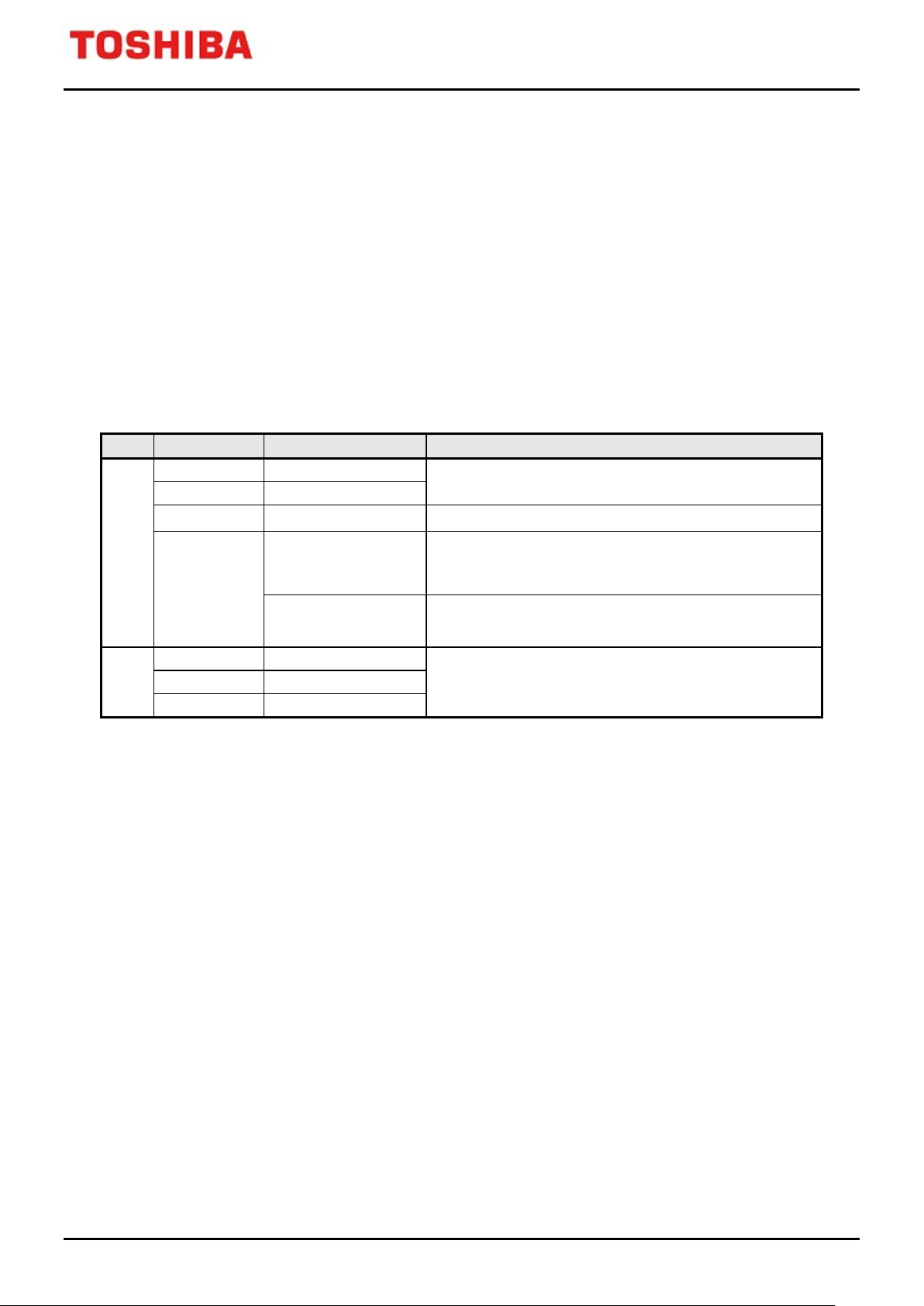
TXZ/TXZ+ Family
35 / 107
Register name
Function
Detail
[13] Phase
setting
[VExVDUTYB]
b-phase voltage duty
[VExVDUTYC]
c-phase voltage duty
Advanced Vector Engine Plus
b. Inverse Clarke transformation
<Equation>
kc = 1 ; Relative transformation
if ([VExFMODE]<CCVMD> = 1) Kc = √(2 / 3) ; Absolute transformation
if ([VExFMODE]<PHCVDIS> = 0) ; 3-phase conversion is enabled.
[VExVDUTYA] = kc / [VExVDC] × [VExVALPHA] + 1 / 2 ; Va Duty
[VExVDUTYB] = kc / [VExVDC] × (-1 / 2 × [VExVALPHA] + √3 / 2 × [VExVBETA]) + 1 / 2 ; Vb Duty
[VExVDUTYC] = kc / [VExVDC] × (-1 / 2 × [VExVALPHA] -√3 / 2 × [VExVBETA]) + 1 / 2 ; Vc Duty
else ; Phase conversion is disabled.
[VExVDUTYA] = 1 /[VExVDC] × [VExVALPHA] + 1 / 2 ; Va Duty
[VExVDUTYB] = 1 /[VExVDC] × [VExVBETA] + 1 / 2 ; Vb Duty
[VExVALPHA]
[VExVBETA]
[VExVDC]
Input
[VExFMODE]
[VExVDUTYA]
Output
α-axis voltage
β-axis voltage
DC supply voltage
[12] Phase
transformation setting
transformation mode
a-phase voltage duty
32-bit fixed-point data (-1.0 to 1.0, 31 fractional bits)
16-bit fixed-point data (0.0 to 1.0, 15 fractional bits)
<PHCVDIS>
0: 2-3 phase transformation is enabled.(3-phase AC output)
1: 2-3 phase transformation is disabled.(2-phase AC output)
<CCVMD>
0: Relative transformation 1: Absolute transformation
32-bit fixed-point data (0.0 to 1.0, 31 fractional bits)
2021-02-24
Rev. 3.1
Page 36

TXZ/TXZ+ Family
36 / 107
Advanced Vector Engine Plus
3.3.4. Output Control
Output control unit converts a 3-phase voltage duty into the PMD setting format. The conversion result is set to
[VExCMPU], [VExCMPV], and [VExCMPW]. According to the output control operation setting, [VExOUTCR]
should be set. Dead time compensation control and PWM output limitation can also be executed.
There are two types of output control task: output control 1 and output control 2. Each task supports different
PWM outputs.
Note: When PMD is set to VE mode, the PMD's [PMDxCMPU]/[PMDxCMPV]/[PMDxCMPW]/
[PMDxMDOUT] registers switch to [VExCMPU]/[VExCMPV]/[VExCMPW]/[VExOUTCR].
Even so, double buffer/triple buffer function of PMD is effective. For details of the buffer function, refer
to "Advanced Programmable Motor Control Circuit" in the reference manual.
When double buffers are enabled with PMD, while the output control 1 task/output control 2 task/trigger
generation task are running, the execution stage is not updated at the execution stage update timing.
3.3.4.1. Output control 1 (Task 0)
Output control 1 task supports normal PWM outputs and PWM outputs in the PWM Shift 1. When PWM Shift is
enabled, if the rotational speed ([VExOMEGA]) is lower than the reference of PWM Shift switch
([VExFPWMCHG]), PWM outputs changes to PWM Shift 1.
Note: PWM Shift 1 can only be selected in the 1-shunt current detection mode.
a. Output conversion
<Equation>
[VExMCTLF]<LAVFM> = [VExMCTLF]<LAVF> ; Updates a previous value of low-speed flag
[VExMCTLF]<PLSLFM> = [VExMCTLF]<PLSLF> ; Updates a previous value of PWM duty check flag
[VExMCTLF] = & 0xFFEE ; Current flag is cleared
if (([VExFMODE]<IDMODE[1]> = 1) & ([VExFMODE]<C2PEN> = 1) & ([VExFMODE]<SPWMEN> = 1))
; Shift 1 is enabled in 1-shunt current and
2-phase modulation modes
if (|[VExOMEGA]| < [VExFPWMCHG]) [VExMCTLF]<LAVF> = 1
; Sets the low-speed flag for low speed
determination
dutya = [VExVDUTYA]
dutyb = [VExVDUTYB]
dutyc = [VExVDUTYC]
if ([VExMCTLF]<LAVF> = 1) ; PWM Shift 1 at low-speed
if ([VExSECTOR] = 0, 3, 4, 7, 8, 11) ; Sector determination
dutya = dutya + [VExTMPREG5] ; Zero-vector V7 transformation
dutyb = dutyb + [VExTMPREG5]
dutyc = dutyc + [VExTMPREG5]
pwma = dutya × 0x8000 ; Transforms the PMD setting value
pwmb = dutyb × 0x8000
pwmc = dutyc × 0x8000
2021-02-24
Rev. 3.1
Page 37
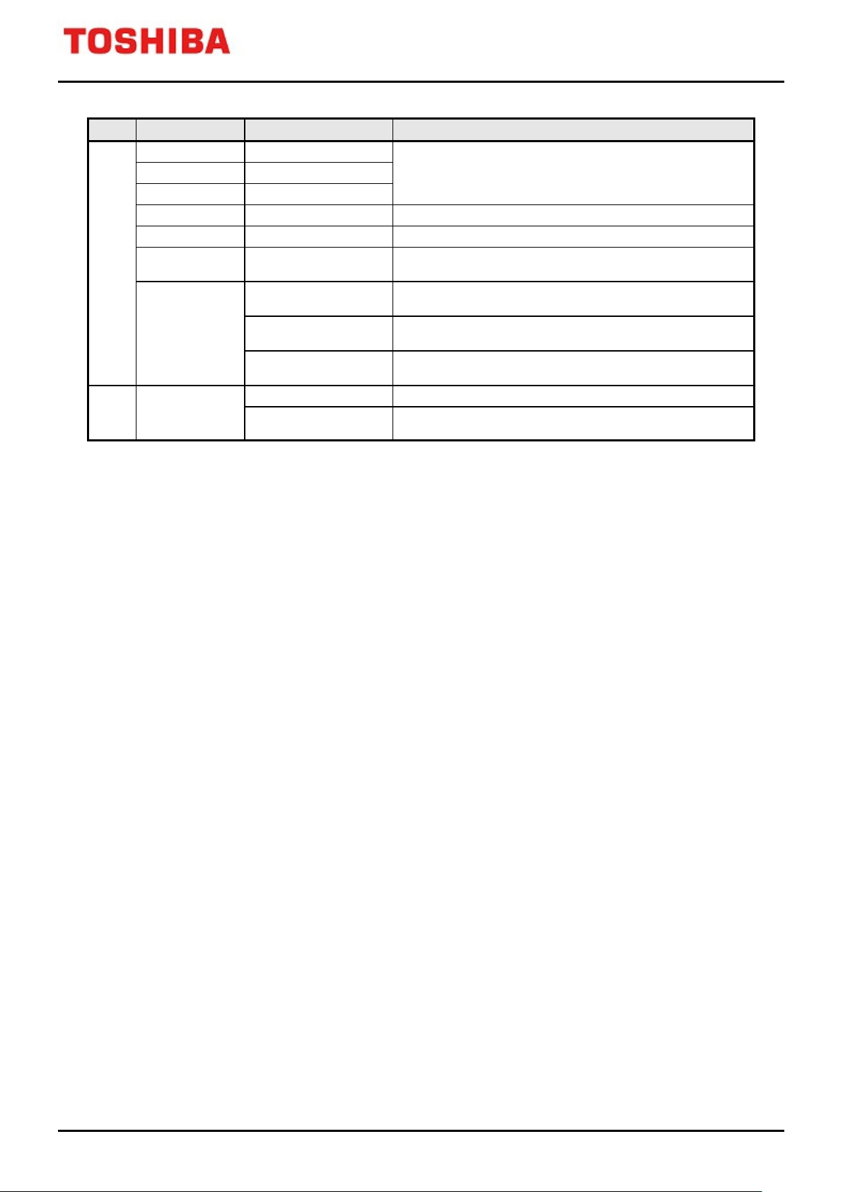
37 / 107
Register name
Function
Detail
PWM Shift switch
reference speed
16-bit fixed-point data (0.0 to 1.0, 15 fractional bits)
Shift switch is disabled when [VExFPWMCHG] = 0x0000
<C2PEN>
0: 3-phase modulation 1: 2-phase modulation
0: Shift is disabled 1: Shift is enabled
[3:2] Current detection
<IDMODE>
00: 3-shunt 01: 2 sensors 10, 11: 1-shunt
[1:0] Low-speed flag
<LAVFM>, <LAVF>
[5:4] PWM duty check
flag
TXZ/TXZ+ Family
Advanced Vector Engine Plus
Input
Output
[VExVDUTYA]
[VExVDUTYB]
[VExVDUTYC]
[VExSECTOR]
[VExOMEGA]
[VExFPWMCHG]
[VExFMODE]
[VExMCTLF]
a-phase voltage duty
b-phase voltage duty
c-phase voltage duty
Sector information 4-bit data
Rotational speed 16-bit fixed-point data (-1.0 to 1.0, 15 fractional bits)
[0] Modulation mode
[1] PWM Shift enable
mode
32-bit fixed-point data (0.0 to 1.0, 31 fractional bits)
<SPWMEN>
<PLSLFM>, <PLSLF>
b. PWM output limitation
<Equation>
if ([VExPWMMAX] = 0) max = 0x8000
else max = [VExPWMMAX]
if ((pwma > max) & (0x8000 > max)) ; Checks the PWM upper-limit for U-phase.
if (([VExMODE]<PWMFLEN> = 0) | (pwma < 0x8000)) ; Confirms the duty of 100% of the output
limitation.
pwma = max
[VExMCTLF]<PWMOVF> = 1
min = [VExPWMMIN]
if ((pwma < min) & (min > 0)) ; Checks the PWM lower-limit for U-phase.
if (([VExMODE]<PWMBLEN> = 0) | (pwma > 0)) ; Confirms the duty of 0% of the output
limitation.
pwma = min
[VExMCTLF]<PWMOVF> = 1
(Calculates the other 2-phase in the same manner)
2021-02-24
Rev. 3.1
Page 38

38 / 107
Register name
Function
Detail
Sets the upper-limit
value of the PWM.
Sets the lower-limit
value of the PWM.
[11] Indicates the excess
limitation.
TXZ/TXZ+ Family
Advanced Vector Engine Plus
[VExPWMMAX]
16-bit data ("0x0000" to "0x8000")
[VExPWMMIN]
Input
Output
[VExMODE]
[VExMCTLF]
[12] Sets the output duty
of 0% when the PWM is
limited.
[13] Sets the output duty
of 100% when the PWM
is limited.
flag of the PWM output
<PWMBLEN>
0: Duty of 0% setting is disabled.
1: Duty of 0% setting is enabled.
<PWMFLEN>
0: Duty of 100% setting is disabled.
1: Duty of 100% setting is enabled.
<PWMOVF>
c. Dead time compensation
<Equation>
if (0 < pwma < 0x8000) dt = [VExDTC]
else dt = 0
if ([VExDTCS]<IASTS> = 001, 101) ; On Positive current
if ([VExMODE]<PMDDTCEN> = 1) ; Sets the dead time correction of the PMD
if (pwma > (0x8000 - 2 × dt)) pwma = (0x8000 + pwma) / 2
else pwma = pwma + dt
if (([VExMODE]<PWMFLEN> = 1) & (max < 0x8000)) ; Confirms the duty of 100%
of the output limitation
if (pwma > (0x8000-1)) pwma = 0x8000 -1 ; Output limitation after correction.
else
if (pwma > 0x8000) pwma = 0x8000 ; Output limitation after correction.
else if ([VExDTCS]<IASTS> = 011, 111) ; On negative current
if ([VExMODE]<PMDDTCEN> = 1) ; Sets the dead time correction of the PMD
if (pwma < (2 × dt)) pwma = pwma / 2
else pwma = pwma - dt
if (([VExMODE]<PWMBLEN> = 1) & (min > 0)) ; Confirms the duty of 0%
of the output limitation.
if (pwma < 1) pwma = 1 ; Output limitation after correction.
else
if (pwma < 0) pwma = 0 ; Output limitation after correction.
(Calculates the other 2-phase in the same manner.)
2021-02-24
Rev. 3.1
Page 39

39 / 107
Register name
Function
Detail
The amount of dead time
compensation
Dead time compensation
TXZ/TXZ+ Family
Advanced Vector Engine Plus
[VExDTC]
[12] Sets the output duty
of 0% when the PWM is
limited PWM.
[13] Sets the output duty
[VExMODE]
Input
[VExDTCS]
of 100% when the PWM
is limited.
[14] Dead time
correction control of the
PMD circuit.
control/status
16-bit data ("0x0000" to "0x8000")
<PWMBLEN>
0: Duty of 0% setting is disabled.
1: Duty of 0% setting is enabled.
<PWMFLEN>
0: Duty of 100% setting is disabled.
1: Duty of 100% setting is enabled.
<PMDDTCEN>
0: PMD dead time correction is disabled.
1: PMD dead time correction is enabled.
<ICSTS>, <IBSTS>, <IASTS>
000, 010, 100, 110: Undefined
001, 101: Positive current
011, 111: Negative current
2021-02-24
Rev. 3.1
Page 40

40 / 107
TXZ/TXZ+ Family
Advanced Vector Engine Plus
d. Output control /PWM Shift 1 transformation
<Equation>
outcr = 0x1FF ; All phases center ON
if ([VExMCTLF]<LAVF> = 1) ; PWM Shift 1 at low-speed
if ([VExSECTOR] = 0, 1, 2, 11) ; V-phase center OFF
outcr = 0x1F3 ; Reverses a V-phase carrier
else if ([VExSECTOR] = 3, 4, 5, 6) ; W-phase center OFF
outcr = 0x1CF ; Reverses a W-phase carrier
else if ([VExSECTOR] = 7, 8, 9, 10) ; U-phase center OFF
outcr = 0x1FC ; Reverses a U-phase carrier
if ([VExMODE]<OCRMD> = 00, 11) ; Output OFF
outcr = 0x000
else if ([VExMODE]<OCRMD> = 10) ; Short circuit brake
outcr = 0x015
[VExCMPU] = pwma
[VExCMPV] = pwmb
[VExCMPW] = pwmc
[VExOUTCR] = outcr
[Pulse width difference check. All OFF-width check]
dif1 = | pwmc - pwma |
dif2 = | pwmb - pwmc |
dif3 = | pwma - pwmb |
difmin = dif1
if (dif2 < difmin) difmin = dif2
if (dif3 < difmin) difmin = dif3 ; Minimum width difference
difmax = (dif1 + dif2 + dif3) / 2 ; Maximum width difference
if ([VExMCTLF]<LAVF> = 1) ; PWM Shift 1 at low-speed
if ([VExSECTOR]<[0]> = 0) difmin = difmax ; Maximum width difference at even sectors
else difmin = difmax-difmin ; Medium width difference at odd sectors
else if ([VExFMODE]<C2PEN> = 1) ;
if ([VExSECTOR] = 0, 3, 4, 7, 8, 11) difmin = difmin × 2 ; Corrected on the sector
(minimum width = minimum width difference)
if (difmid < difmin) difmin = difmid ; Check the minimum width difference
after correction
dmax = pwma
if (pwmb > dmax) dmax = pwmb
if (pwmc > dmax) dmax = pwmc ; Minimum width
offmin = 1-dmax ; All OFF-width
if ([VExMODE]<OCRMD> = 01) ; Output enable
if ([VExFMODE]<IDMODE[1]> = 1)) ; 1-shunt current detection
if (difmin < [VExMINPLS]) [VExMCTLF]<PLSLF> = 1 ; Check the minimum width difference
else ; 3-shunt, 2 sensors
if (offmin < [VExMINPLS]) [VExMCTLF]<PLSLF> = 1 ; All OFF-width check
Normal PWM at 2-phase modulation
2021-02-24
Rev. 3.1
Page 41
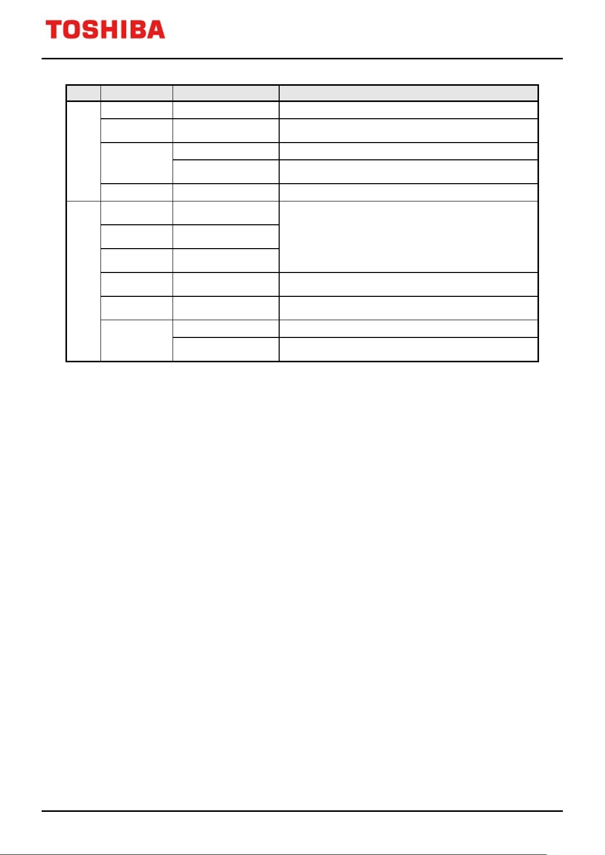
41 / 107
Register name
Function
Detail
[3:2] Output control
operation
mode
U-phase PWM duty
setting of the PMD
V-phase PWM duty
setting of the PMD
W-phase PWM duty
setting of the PMD
PMD output control
setting
PMD EMG release
command
[5:4] PWM duty check
flag
TXZ/TXZ+ Family
Advanced Vector Engine Plus
Input
Output
[VExSECTOR]
[VExMODE]
[VExFMODE]
[VExMINPLS]
[VExCMPU]
[VExCMPW]
[VExOUTCR]
[VExEMGRS]
[VExMCTLF]
Sector information
[0] Modulation mode
[3:2] Current detection
Minimum pulse width 16-bit data
[1:0] Low Speed flag
4-bit data
<OCRMD>
<C2PEN>
<IDMODE>
16-bit data ("0x0000" to "0x8000") [VExCMPV]
9-bit setting
1-bit setting
<LAVFM>, <LAVF>
<PLSLFM>, <PLSLF>
2021-02-24
Rev. 3.1
Page 42
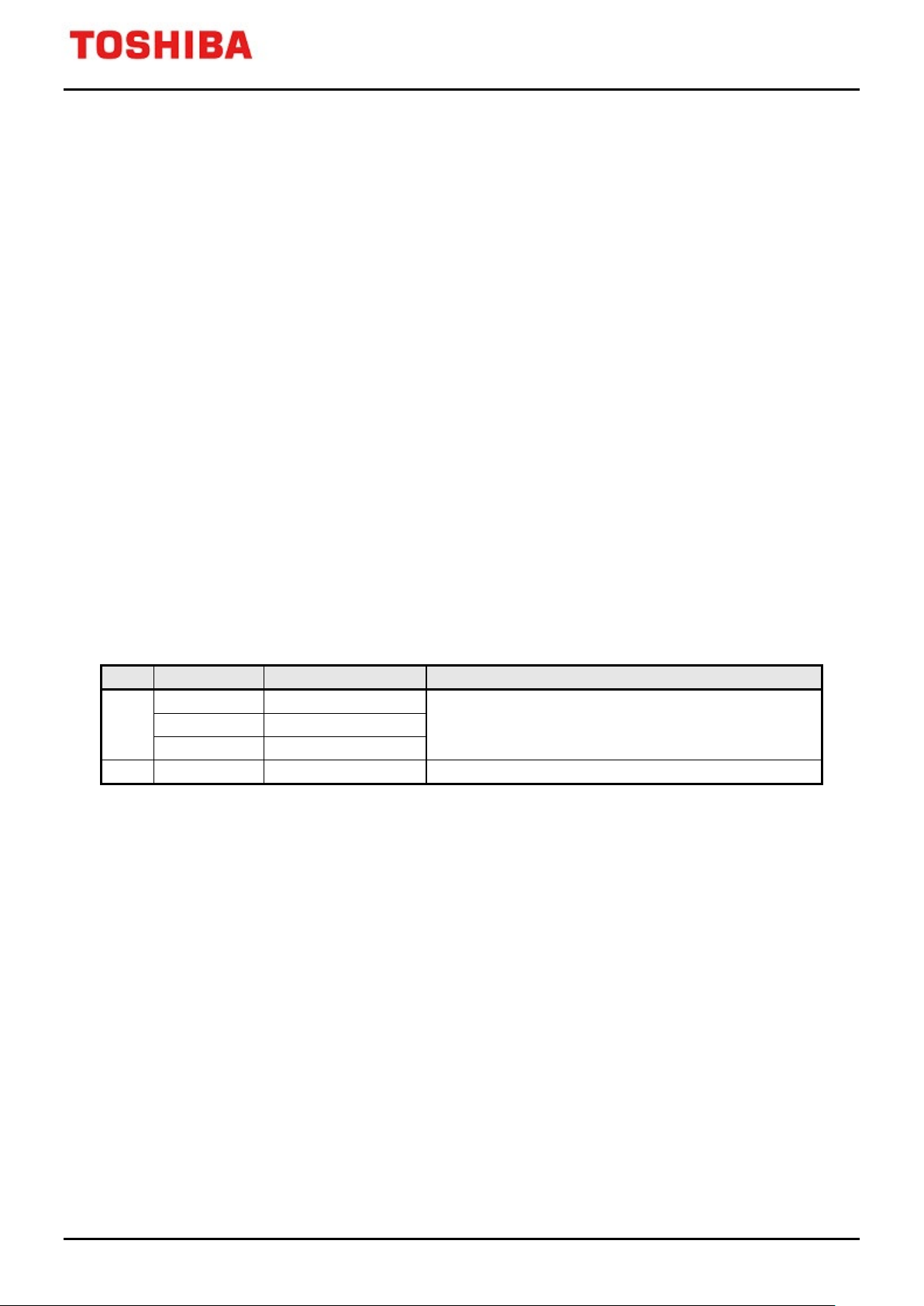
TXZ/TXZ+ Family
42 / 107
Register name
Function
Detail
[VExVDUTYA]
a-phase voltage duty
[VExVDUTYB]
b-phase voltage duty
[VExVDUTYC]
[VExMCTLF]
Advanced Vector Engine Plus
3.3.4.2. Output control 2 (Task 9)
Output control 2 task supports two mode outputs: normal PWM outputs and PWM outputs in PWM Shift 2.
When the PWM output in PWM Shift 2 is set, enable PWM Shift ([VExFMODE]<SPWMEN> = 1) and select the
value other than "00" for PWM Shift mode selection ([VExFMODE]<SPWMMD>).
Note: PWM Shift can be selected only in 1-shunt current detection mode.
a. Output conversion
<Equation>
mctlfm = [VExMCTLF] ; Read the flag register.
mctlfm = & 0x0011 ; Extracts the current value flag
mctlfm = mctlfm << 1 ; Shifts to the previous value
if (|[VExOMEGA]| < [VExFPWMCHG]) mctlfm[0] = 1 ; Sets a low-speed flag based on low-speed
determination
[VExMCTLF] = & 0xFFCC ; Current flag is cleared.
[VExMCTLF] = | mctlfm ; Update the flag.
pwma = [VExVDUTYA] × 0x8000 ; The setting value of the PMD is converted.
pwmb = [VExVDUTYB] × 0x8000
pwmc = [VExVDUTYC] × 0x8000
Input
c-phase voltage duty
Output
[1:0] Low-speed flag <LAVFM>, <LAVF>
32-bit fixed-point data (0.0 to 1.0, 31 fractional bits)
2021-02-24
Rev. 3.1
Page 43
TXZ/TXZ+ Family
43 / 107
Register name
Function
Detail
Sets the upper-limit
value of the PWM.
Sets the lower-limit
value of the PWM.
[11] Indicates the excess
limitation.
Advanced Vector Engine Plus
b. PWM output limitation
<Equation>
if ([VExPWMMAX] = 0) max = 0x8000
else max = [VExPWMMAX]
if (pwma > max) & (0x8000 > max)) ; Checks the PWM upper-limit for U-phase.
if (([VExMODE]<PWMFLEN> = 0) | (pwma < 0x8000)) ; Confirms the duty of 100% of the output
limitation.
pwma = max
[VExMCTLF]<PWMOVF> = 1
min = [VExPWMMIN]
if ((pwma < min) & (min > 0)) ; Checks the PWM lower-limit for U-phase.
if (([VExMODE]<PWMBLEN> = 0) | (pwma > 0)) ; Confirms the duty of 0% of the output
limitation.
pwma = min
[VExMCTLF]<PWMOVF> = 1
(Calculates the other 2-phase in the same manner)
[VExPWMMAX]
[VExPWMMIN]
Input
Output
[VExMODE]
[VExMCTLF]
[12] Sets the output duty
of 0% when the PWM is
limited.
[13] Sets the output duty
of 100% when the PWM
is limited.
flag of the PWM output
16-bit data ("0x0000" to "0x8000")
<PWMBLEN>
0: Duty of 0% setting is disabled.
1: Duty of 0% setting is enabled.
<PWMFLEN>
0: Duty of 100% setting is disabled.
1: Duty of 100% setting is enabled.
<PWMOVF>
2021-02-24
Rev. 3.1
Page 44

TXZ/TXZ+ Family
44 / 107
Register name
Function
Detail
The amount of dead time
compensation
Dead time compensation
Advanced Vector Engine Plus
c. Dead time compensation
<Equation>
if (0 < pwma < 0x8000) dt = [VExDTC]
else dt = 0
if ([VExDTCS]<IASTS> = 001, 101) ; On Positive current
if ([VExMODE]<PMDDTCEN> = 1) ; Sets the dead time correction of the PMD
if (pwma > (0x8000- 2 × dt)) pwma = (0x8000 + pwma) / 2
else pwma = pwma + dt
if (([VExMODE]<PWMFLEN> = 1) & (max < 0x8000)) ; Confirms the duty of 100%
of the output limitation
if (pwma > (0x8000-1)) pwma = 0x8000 -1 ; Output limitation after correction.
else
if (pwma > 0x8000) pwma = 0x8000 ; Output limitation after correction.
else if ([VExDTCS]<IASTS> = 011, 111) ; On negative current
if ([VExMODE]<PMDDTCEN> = 1) ; Sets the dead time correction of the PMD
if (pwma < (2 × dt)) pwma = pwma / 2
else pwma = pwma - dt
if (([VExMODE]<PWMBLEN> = 1) & (min > 0)) ; Confirms the duty of 0%
of the output limitation.
if (pwma < 1) pwma = 1 ; Output limitation after correction.
else
if (pwma < 0) pwma = 0 ; Output limitation after correction.
(Calculates the other 2-phase in the same manner.)
[VExDTC]
[12] Sets the output duty
of 0% when the PWM is
limited PWM.
[13] Sets the output duty
Input
[VExMODE]
[VExDTCS]
of 100% when the PWM
is limited.
[14] Dead time
correction control of the
PMD circuit.
control/status
16-bit data ("0x0000" to "0x8000")
<PWMBLEN>
0: Duty of 0% setting is disabled.
1: Duty of 0% setting is enabled.
<PWMFLEN>
0: Duty of 100% setting is disabled.
1: Duty of 100% setting is enabled.
<PMDDTCEN>
0: PMD dead time correction is disabled.
1: PMD dead time correction is enabled.
<ICSTS>, <IBSTS>, <IASTS>
000, 010, 100, 110: Undefined
001, 101: Positive current 011, 111: Negative current
2021-02-24
Rev. 3.1
Page 45

TXZ/TXZ+ Family
45 / 107
Advanced Vector Engine Plus
d. Output control /PWM Shift 2 transformation
<Equation>
outcr = 0x1FF ; All phases center ON
if (([VExFMODE]<IDMODE[1]> = 1) & ([VExFMODE]<SPWMEN> = 1)) ; PWM Shift 2 is enabled in
1-shunt
if ([VExOMEGA] > [VExFPWMCHG]) ; Shift 2 control area determination
if ([VExFMODE]<SPWMMD> = 01) ; Shift 2, U-phase reference
if (pwma < 0x4000) outcr = 0x1FC ; Reverses a U-phase carrier
else if ([VExFMODE]<SPWMMD> = 10) ; Shift 2, V-phase reference
if (pwmb < 0x4000) outcr = 0x1F3 ; Reverses a V-phase carrier
else if ([VExFMODE]<SPWMMD> = 11) ; Shift 2, W-phase reference
if (pwmc < 0x4000) outcr = 0x1CF ; Reverses a W-phase carrier
if ([VExMODE]<OCRMD> = 00, 11) outcr = 0x000 ; Output OFF
else if ([VExMODE]<OCRMD> = 10) outcr = 0x015 ; Short circuit brake
[VExCMPU] = pwma
[VExCMPV] = pwmb
[VExCMPW] = pwmc
[VExOUTCR] = outcr
[Pulse width check]
if ([VExFMODE]<IDMODE[1]> = 1 & [VExFMODE]<SPWMEN> = 1) ; Reference phase for Shift 2
is double width.
if ([VExFMODE]<SPWMMD> = 01) pwma = pwma / 2 ; U-phase reference
else if ([VExFMODE]<SPWMMD> = 10) pwmb = pwmb / 2 ; V-phase reference
else if ([VExFMODE]<SPWMMD> = 11) pwmc = pwmc / 2 ; W-phase reference
; Detection correction for shift 2 carrier inversion control (Off time/ 2 < [VExMINPLS])
if ([VExOUTCR] = 0x1FC) pwma = 0x4000 + pwma
else if ([VExOUTCR] = 0x1F3) pwmb = 0x4000 + pwmb
else if ([VExOUTCR] = 0x1CF) pwmc = 0x4000 + pwmc
dmin = pwma
if (pwmb < dmin) dmin = pwmb
if (pwmc < dmin) dmin = pwmc ; Minimum ON width
dmax = pwma
if (pwmb > dmax) dmax = pwmb
if (pwmc > dmax) dmax = pwmc ; Maximum ON width
offmin = 1-dmax ; Minimum OFF width (All OFF period)
if (dmin > offmin) dmin = offmin ; Detects the minimum ON/OFF width
minpls = [VExMINPLS]
if ([VExMODE]<OCRMD> = 00, 10, 11) minpls = 0x0000 ; If output is not enabled
if ([VExFMODE]<IDMODE[1]> = 1) ; 1-shunt (PWM Shift 2)
if (offmin < minpls [VExMCTLF]<PLSLF> = 1 ; ALL OFF width
else
if (dmin < minpls) [VExMCTLF]<PLSLF> = 1 ; Detects the minimum ON/OFF width
2021-02-24
Rev. 3.1
Page 46
46 / 107
Register name
Function
Detail
U-phase PWM setting
of the PMD
V-phase PWM setting
of the PMD
W-phase PWM setting
of the PMD
PMD output control
setting
PMD EMG release
command
flag
TXZ/TXZ+ Family
Advanced Vector Engine Plus
Input
Output
[VExFPWMCHG]
[VExMODE]
[VExMINPLS]
[VExFMODE]
[VExCMPU]
[VExCMPV]
[VExCMPW]
[VExOUTCR]
PWM Shift switch
reference speed
[3:2] Output control
operation
Minimum pulse width
[1] PWM Shift enable
[3:2] Current detection
mode
[15:14] PWM Shift
mode
16-bit fixed-point data (0.0 to 1.0, 15 fractional bits)
Shift switch is disabled when [VExFPWMCHG] = 0x0000
<OCRMD>
00: Output is disabled.
01: Output is enabled.
10: Short circuit brake.
11: EMG release.
16-bit data
<SPWMEN>
0: Shift is disabled 1: Shift is enabled
<IDMODE[1:0]>
00: 3-shunt 01: 2 sensors 10, 11: 1-shunt
<SPWMMD>
00: Shift 1
01: Shift 2 (U-phase Center PWM)
10: Shift 2 (V-phase Center PWM)
11: Shift 2 (W-phase Center PWM)
16-bit data ("0x0000" to "0x8000")
9-bit setting
[VExEMGRS]
[VExMCTLF]
[5:4] PWM duty check
1-bit setting
<PLSLFM>, <PLSLF>
2021-02-24
Rev. 3.1
Page 47
TXZ/TXZ+ Family
47 / 107
Current detection
<SPWMMD>
2-phase/
3-phase
2-phase/
3-phase
[VExTRGCMP0] = 0x3FFF + (dmin + dmid) / 4 + [VExTRGCRC]
[VExTRGCMP1] = 0x3FFF + (dmax + dmid) / 4 + [VExTRGCRC]
[VExTRGCMP0] = 0x3FFF + [VExTRGCRC]
[VExTRGCMP1] = 0x3FFF + (dmax + dmid) / 4 + [VExTRGCRC]
[VExTRGCMP0] = 0x3FFF + [VExTRGCRC]
[VExTRGCMP1] = 0x3FFF + (dmax + dmid) / 4 + [VExTRGCRC]
0x3FFF +
[VExTRGCMP1] = 0x7FFF - [VExTADC] + [VExTRGCRC]
0x3FFF - (dmax + dmid) / 4 +
[VExTRGCMP1] = 0x3FFF - (dmin + dmid) / 4 + [VExTRGCRC]
[VExTRGCMP0] = 0x3FFF - (dmax + dmid) / 4 + [VExTRGCRC]
[VExTRGCMP1] = 0x3FFF + [VExTRGCRC]
[VExTRGCMP0] = 0x3FFF - (dmax + dmid) / 4 + [VExTRGCRC]
[VExTRGCMP1] = 0x3FFF + [VExTRGCRC]
[VExTRGCMP0] = 0x0000 + [VExTADC] + [VExTRGCRC]
[VExTRGCMP1] = 0x3FFF + [VExTRGCRC]
Advanced Vector Engine Plus
3.3.5. Trigger Generation (Task 1)
The trigger generation unit calculates the synchronous trigger timing for ADC from the PWM duty setting values
([VExCMPU], [VExCMPV], and [VExCMPW]) based on the current detection method, and sets it to the
[VExTRGCMP0] and [VExTRGCMP1] registers.
Note 1: [VExTRGCMP0] and [VExTRGCMP1] are updated only in 1-shunt current detection
Note 2: [VExTRGCMP0] and [VExTRGCMP1] are not updated when PWM Shift 2 is selected.
Note 3: Please select "Compare to basic carrier" in the trigger control register comparison carrier selection
[PMDxTRGCR]<CARSEL> of the PMD.
Note 4: [VExTRGCMP0] / [VExTRGCMP1] / [VExTRGSEL] switches to [PMDxTRGCMP0] /
[PMDxTRGCMP1] / [PMDxTRGSEL] register of PMD when PMD is set to VE mode. Even in that
case, double buffer / triple buffer function of PMD is effective. When double buffers / triple buffers are
enabled in the PMD, the execution stage is updated even when the update timing of the double buffer /
triple buffer execution stage is reached while the output control 1 task/output control 2 task/trigger
generation task is being executed not.
Note 5: For details of PMD, refer to "Advanced Programmable Motor Control Circuit" in the reference manual.
mode
<IDMODE>
PWM Shift
setting
<SPWMEN>
Modulation
mode
<C2PEN>
Low-speed
flag
<LAVF >
Trigger generation formula
3-shunt -
2 sensors -
Disable
PWM Shift
1-shunt
(Latter half)
PWM Shift 1 2-phase
PWM Shift 2 3-phase - (No trigger generation)
Disable
PWM Shift
1-shunt
(First half)
PWM Shift 1 2-phase
PWM Shift 2 3-phase - (No trigger generation)
3-phase -
2-phase -
3-phase -
2-phase -
- (No trigger generation)
- (No trigger generation)
High-speed
Low-speed
High-speed
Low-speed
[VExTRGCMP0] =
[VExTRGCMP0] =
[VExTRGCRC]
[VExTRGCRC]
Note: dmin: A value on the minimum duty phase, dmax: A value on the maximum duty phase, dmid: A value
on the medium duty phase
2021-02-24
Rev. 3.1
Page 48
48 / 107
Register name
Function
Detail
U-phase PWM duty
setting of the PMD
V-phase PWM duty
setting of the PMD
W-phase PWM duty
setting of the PMD
[8] Trigger correction
enable
PMD trigger 0 timing
setting
PMD trigger 1 timing
setting
PMD trigger selection
setting
TXZ/TXZ+ Family
Advanced Vector Engine Plus
[VExCMPU]
16-bit data ("0x0000" to "0x8000") [VExCMPV]
[VExCMPW]
Input
[VExTADC]
[VExTRGCRC]
[VExSECTOR]
[VExMODE]
[VExFMODE]
ADC conversion time
Trigger correction value 16-bit data ("0x0000" to "0x8000")
Sector information
[0] Zero-current
detection
[3:2] Output control
operation
[0] Modulation mode
[1] PWM Shift enable
[3:2] Current detection
mode
[15:14] PWM Shift mode
16-bit data ("0x0000" to "0x8000")
4-bit data
<ZIEN>
0: Normal current detection
1: Zero-current detection
<OCRMD>
00: Output is disabled.
01: Output is enabled.
10: Short circuit brake.
11: EMG release.
<C2PEN>
0: 3-phase modulation 1: 2-phase modulation
<SPWMEN>
0: Shift is disabled 1: Shift is enabled
<IDMODE[1:0]>
00: 3-shunt 01: 2 sensors 10, 11: 1-shunt
<CRCEN>
<SPWMMD>
00: Shift 1
01: Shift 2 (U-phase Center PWM)
10: Shift 2 (V-phase Center PWM)
11: Shift 2 (W-phase Center PWM)
Output
[VExMCTLF]
[VExTRGCMP0]
[VExTRGCMP1]
[VExTRGSEL]
[0] Low-speed flag
<LAVF>
16-bit data ("0x0001" to "0x7FFF")
3-bit data: [VExSECTOR] / 2
2021-02-24
Rev. 3.1
Page 49

TXZ/TXZ+ Family
49 / 107
Advanced Vector Engine Plus
3.3.6. Input Process
In the input process, the vector engine reads conversion results and phase information from the ADC. Depending
on the current detection method and PWM Shift mode setting, the vector engine converts the phase current data
and the voltage data into the fixed-point format and stores them in predefined registers.
In zero-current detection mode, current detection results are stored in the zero-current register.
The vector engine specifies the hysteresis width to determine the current polarity for dead time compensation
control.
There are two types of input process: Input process 1 task and Input process 2 task. Each task supports different
current detection method.
3.3.6.1. Input process 1 (Task 2)
Input process 1 task supports 3-shunt current detection (only 2-phase current detection (Note 1)) and 1-shunt
current detection. However, 1-shunt current detection is not available in PWM Shift 2 (Note 2).
Note 1: Current detection result is used only for two phases. Remained one phase is calculated.
Note 2: PWM Shift can only be selected in 1-shunt current detection mode.
a. Input conversion
<Equation>
[VDC fixed-point transformation/store]
if ([VExMODE]<VDCSEL> = 0) [VExVDC] = [DC voltage] >>1
else [VExVDCL] = [DC voltage] >>1
lavfm = [VExMCTLF]<LAVFM> ; Previous low-speed flag
if ([VExFMODE]<MREGDIS> = 1) ; Previous value invalid.
lavfm = [VExMCTLF]<LAVF> ; Current low-speed flag
[Current 1 read]
if ([VExFMODE]<IDMODE> = 10, 11) ; 1-shunt
if (lavfm = 0) ; Normal PWM
if ([VExSECTORM] = 4, 5, 6, 7) [VExIAADC] = [Current 1]
else if ([VExSECTORM] = 8, 9, 10, 11) [VExIBADC] = [Current 1]
else if ([VExSECTORM] = 0, 1, 2, 3) [VExICADC] = [Current 1]
else if (lavfm = 1) ; PWM Shift 1
if ([VExSECTORM] = 1, 2, 7, 8) [VExIAADC] = [Current 1]
else if ([VExSECTORM] = 0, 5, 6, 11) [VExIBADC] = [Current 1]
else if ([VExSECTORM] = 3, 4, 9, 10) [VExICADC]
if ([VExFMODE]<IDMODE> = 00, 01) ; 3-shunt, 2 sensors
if ([Current 1 phase information] = 1) [VExIAADC] = [Current 1]
else if ([Current 1 phase information] = 2) [VExIBADC] = [Current 1]
else if ([Current 1 phase information] = 3) [VExICADC] = [Current 1]
[Current 2 read]
if ([VExFMODE]<IDMODE> = 10, 11) ; 1-shunt
if (lavfm = 0) ; Normal PWM
if ([VExSECTORM] = 0, 1, 10, 11) [VExIAADC] = [Current 2]
else if ([VExSECTORM] = 2, 3, 4, 5) [VExIBADC] = [Current 2]
else if ([VExSECTORM] = 6, 7, 8, 9) [VExICADC] = [Current 2]
= [Current 1]
2021-02-24
Rev. 3.1
Page 50

TXZ/TXZ+ Family
50 / 107
Advanced Vector Engine Plus
else if (lavfm = 1) ; PWM Shift 1
if ([VExSECTORM] = 3, 4, 9, 10) [VExIAADC] = [Current 2]
else if ([VExSECTORM] = 1, 2, 7, 8) [VExIBADC] = [Current 2]
else if ([VExSECTORM] = 0, 5, 6, 11) [VExICADC] = [Current 2]
if ([VExFMODE]<IDMODE> = 00, 01) ; 3-shunt, 2 sensors
if ([Current 2 phase information] = 1) [VExIAADC] = [Current 2]
else if ([Current 2 phase information] = 2) [VExIBADC] = [Current 2]
else if ([Current 2 phase information] = 3) [VExICADC] = [Current 2]
[Current 3 read]
if ([VExFMODE]<IDMODE[1]> = 1) ; Except 1-shunt
if ([Current 3 phase information] = 1) [VExIAADC] = [Current 3]
else if ([Current 3 phase information] = 2) [VExIBADC] = [Current 3]
else if ([Current 3 phase information] = 3) [VExICADC] = [Current 3]
[Current fixed-point transformation]
ia = [VExIAO] - [VExIAADC]
ib = [VExIBO] - [VExIBADC]
ic = [VExICO] - [VExICADC]
if ([VExFMODE]<IDMODE> = 10, 11) ; 1-shunt
if (lavfm = 0) ; Normal PWM
if ([VExSECTORM] = 0, 1
else if ([VExSECTORM] = 2, 3, 4, 5) ib = -ib
else if ([VExSECTORM] = 6, 7, 8, 9) ic = -ic
else if (lavfm = 1) ; PWM Shift 1
if ([VExSECTORM] = 1, 2, 5, 6, 9, 10) ia = -ia
ib = -ib
ic = -ic
[Current 3 calculation]
n = 6 - [Current 2 phase information] -[Current 1 phase information] ; Calculates the phase number
of Current 3
if (n = 1) ia = -ib -ic
else if (n = 2) ib = -ic -ia
else if (n = 3) ic = -ia -ib
[Current storage]
[VExIA] = ia
[VExIB] = ib
[VExIC] = ic
, 10, 11) ia = -ia
2021-02-24
Rev. 3.1
Page 51
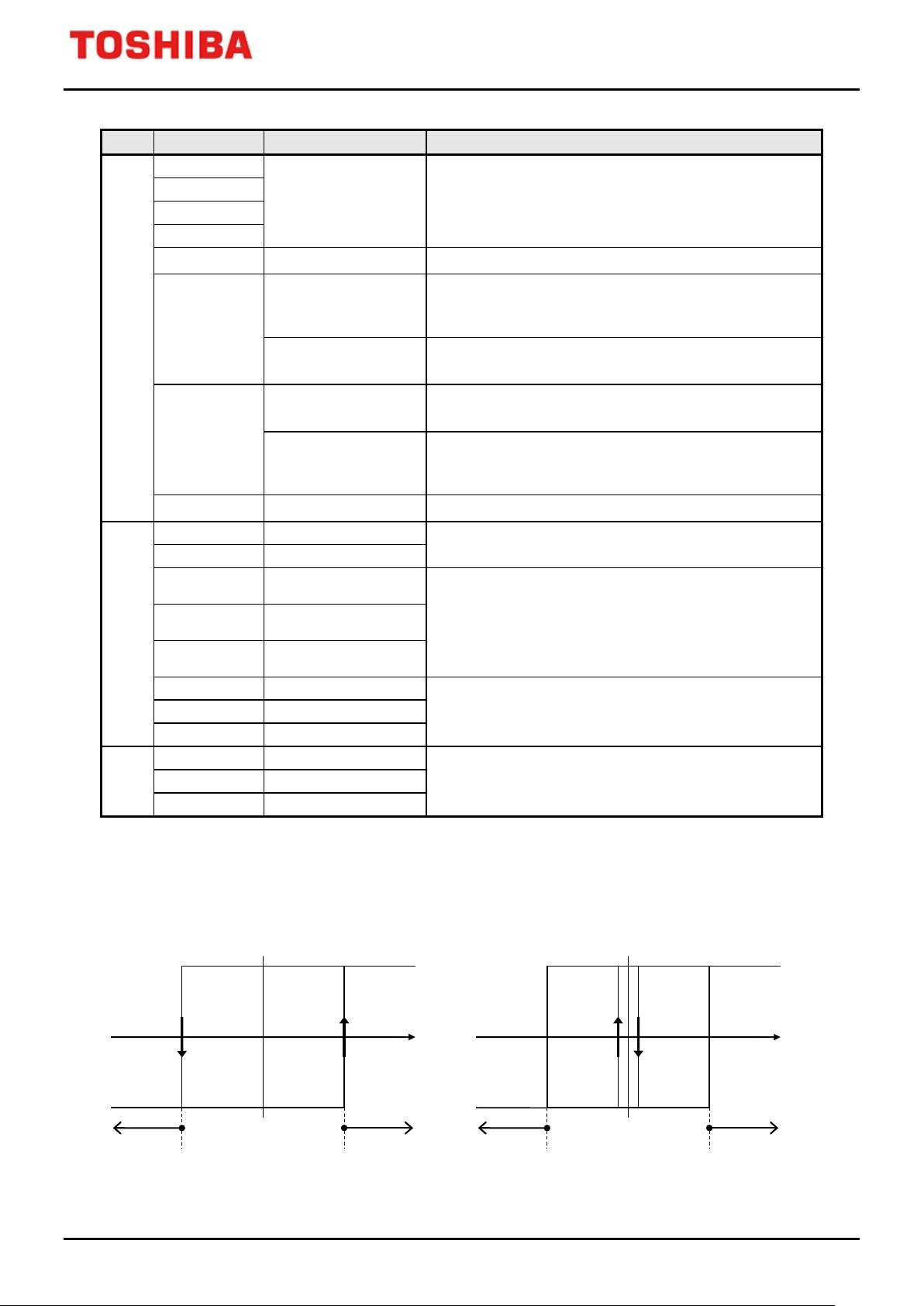
51 / 107
Register name
Function
Detail
[VExVDC]
DC supply voltage
[VExVDCL]
DC supply voltage
The ADC conversion
result of a-phase current
The ADC conversion
result of b-phase current
The ADC conversion
result of c-phase current
b-phase current
[VExICO]
c-phase zero-current
Positive
polarity
Negative
polarity
Hysteresis: 0 ≥ HYS
-HYS +HYS
Reverse hysteresis: HYS < 0
-HYS +HYS
-HYS2
+HYS2
- Stable area
+ Stable area
[ |HYS2| ≤ I, I ≤ -|HYS2|, I > HYS, I < -HYS ]
[ |HYS2| ≤ I, I ≤ -|HYS2|, I > HYS, I < -HYS ]
+ Stable area
- Stable area
Positive
polarity
Negative
polarity
Input
(DC voltage)
(Current 1)
(Current 2)
(Current 3)
[VExSECTORM] Previous [VExSECTOR] 4-bit data
[VExMODE]
Input of the ADC
conversion result
[1] Zero-current detection
[4] Selection VDC store
register
16-bit data (The conversion result is stored in the upper 12
bits.)
<ZIEN>
0: Normal current detection
1: Zero-current detection
<VDCSEL>
0: [VExVDC] 1: [VExVDCL]
TXZ/TXZ+ Family
Advanced Vector Engine Plus
[3:2] Current detection
mode
Output
Internal
[VExFMODE]
[VExMCTLF]
[VExIAADC]
[VExIBADC]
[VExICADC]
[VExIA]
[VExIB]
[VExIC]
[VExIAO]
[VExIBO]
[9] Selects to store the
previous
value(<LAVFM>)
[1:0] Low-speed flag
a-phase current
c-phase current
a-phase zero-current
b-phase zero-current
b. Current polarity determination
<IDMODE>
00: 3-shunt 01: 2 sensors 10, 11: 1-shunt
<MREGDIS>
0: Previous value is maintained.
1: Previous value is not maintained.
<LAVFM>, <LAVF>
16-bit fixed-point data (0.0 to 1.0, 15 fractional bits)
16-bit data (The result is stored in the upper 12 bits.)
32-bit fixed-point data (-1.0 to 1.0, 31 fractional bits)
16-bit data (The result is stored in the upper 12 bits.)
2021-02-24
Rev. 3.1
Page 52
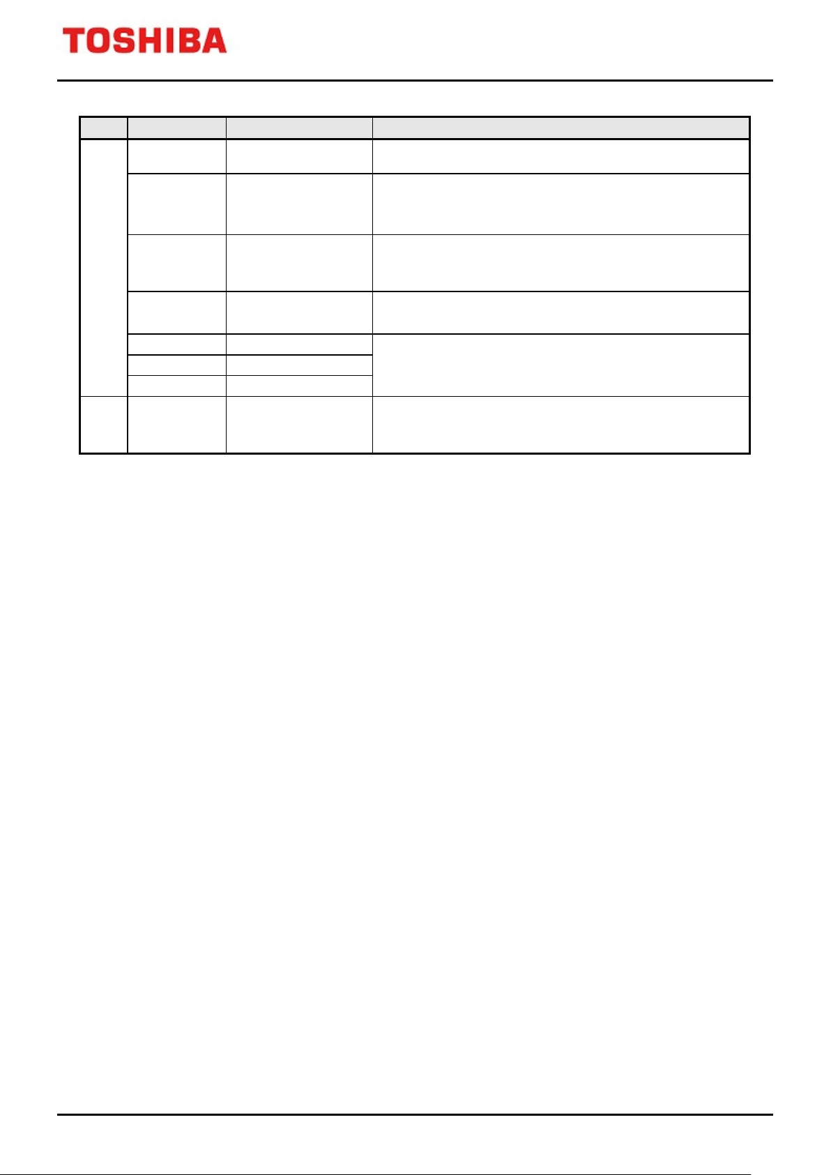
52 / 107
Register name
Function
Detail
Hysteresis for current
polarity determination
[VExIB]
b-phase current
[VExIC]
TXZ/TXZ+ Family
Advanced Vector Engine Plus
Input
Output
[VExHYS]
[VExHYS2]
[VExDTCS]
[VExMODE]
[VExIA]
[VExDTCS]
Hysteresis 2 for current
polarity determination
Dead time compensation
control/status
[15] Current polarity
determination control
a-phase current
c-phase current
Dead time compensation
control/status
16-bit fixed-point data (-1.0 to 1.0, 15 fractional bits)
Polarity determination level on reverse hysteresis ([VExHYS] < 0).
16-bit fixed-point data (0 to 1.0, 15 fractional bits)
This register is invalid when [VExHYS] ≥ 0.
<ICSTS>, <IBSTS>, <IASTS>
000, 010, 100, 110: Undefined
001, 101: Positive current 011, 111: Negative current
<IPDEN>
0: Determination is disabled. 1: Determination is enabled.
32-bit fixed-point data (-1.0 to 1.0, 31 fractional bits)
<ICSTS>, <IBSTS>, <IASTS>
000, 010, 100, 110: Undefined
001, 101: Positive current 011, 111: Negative current
3.3.6.2. Input process 2 (Task 10)
Input process 2 task supports 3-shunt current detection (3-phase detection and 2-phase detection) and 2-sensor
current detection. It also supports 1-shunt current detection when PWM outputting in PWM Shift 2.
A current direction can be specified in each phase.
Note: The zero-current detection mode is not available in input process 2 task.
Note: PWM Shift 2 can only be selected in 1-shunt current detection mode.
a. Input conversion
<Equation>
[VDC fixed-point transformation/store]
if ([VExMODE]<VDCSEL> = 0) [VExVDC] = [DC voltage] >> 1
else [VExVDCL] = [DC voltage] >> 1
[Current 1 read]
if (([VExFMODE]<IDMODE[1]> = 1) & ([VExMCTLF]<[1:0]> = 01, 10, 11)) ; 1-shunt at high-speed
if ([VExFMODE]<SPWMMD> = 01) noc = [VExOUTCR]<UOC>
if ([VExFMODE]<SPWMMD> = 10) noc = [VExOUTCR]<VOC>
if ([VExFMODE]<SPWMMD> = 11) noc = [VExOUTCR]<WOC>
if (noc = 11)
if ([Current 1 phase information] = 1) [VExIAADC] = [Current 1]
else if ([Current 1 phase information] = 2) [VExIBADC] = [Current 1]
else if ([Current 1 phase information] = 3) [VExICADC] = [Current 1]
else if (noc = 00)
if ([Current 2 phase information] = 1) [VExIAADC] = [Current 1]
else if ([Current 2 phase information] = 2) [VExIBADC] = [Current 1]
else if ([Current 2 phase information] = 3) [VExICADC] = [Current 1]
2021-02-24
Rev. 3.1
Page 53

TXZ/TXZ+ Family
53 / 107
Advanced Vector Engine Plus
[Current 2 read]
if (noc = 11)
if ([Current 2 phase information] = 1) [VExIAADC] = [Current 2]
else if ([Current 2 phase information] = 2) [VExIBADC] = [Current 2]
else if ([Current 2 phase information] = 3) [VExICADC] = [Current 2]
if (noc = 00)
if ([Current 1 phase information] = 1) [VExIAADC] = [Current 2]
else if ([Current 1 phase information] = 2) [VExIBADC] = [Current 2]
else if ([Current 1 phase information] = 3) [VExICADC] = [Current 2]
[Current 3 read]
if ([VExFMODE]<IDMODE> = 00 ; Only when 3-phase detection is performed.
if ([Current 3 phase information] = 1) [VExIAADC] = [Current 3]
else if ([Current 3 phase information] = 2) [VExIBADC] = [Current 3]
else if ([Current 3 phase information] = 3) [VExICADC] = [Current 3]
[Current fixed-point transformation]
ia = [VExIAO] - [VExIAADC]
ib = [VExIBO] - [VExIBADC]
ic = [VExICO] - [VExICADC]
if (noc = 11)
if ([VExFMODE]<IAPLMD> = 1) ia = -ia ; Sets direction of Ia current detection
if ([VExFMODE]<IBPLMD> = 1) ib = -ib ; Sets direction of Ib current detection
if ([VExFMODE]<ICPLMD> = 1) ic = -ic ; Sets direction of Ic current detection
if (noc =
if ([VExFMODE]<IAPLMD> = 0) ia = -ia ; Sets direction of Ia current detection
if ([VExFMODE]<IBPLMD> = 0) ib = -ib ; Sets direction of Ib current detection
if ([VExFMODE]<ICPLMD> = 0) ic = -ic ; Sets direction of Ic current detection
n = 6 - [ Current 2 phase information] - [ Current 1 phase information]
if ([VExFMODE]<IDMODE> = 00) ; Current 3 is calculated except when 3-phase
detection is performed.
if (n = 1) ia = -ib -ic
else if (n = 2) ib = -ic -ia
else if (n = 3) ic = -ia -ib
[Current storage]
[VExIA] = ia
[VExIB] = ib
[VExIC] = ic
00)
2021-02-24
Rev. 3.1
Page 54
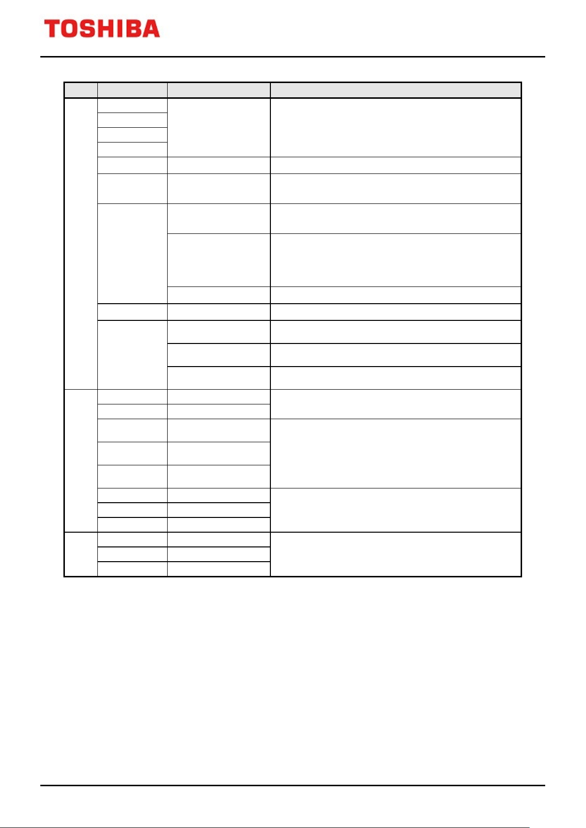
54 / 107
Register name
Function
Detail
[1:0] U-phase output
control
control
[5:4] W-phase output
control
[VExVDC]
DC supply voltage
[VExVDCL]
DC supply voltage
The ADC conversion
result of a-phase current
The ADC conversion
result of b-phase current
The ADC conversion
result of c-phase current
[VExICO]
c-phase zero-current
TXZ/TXZ+ Family
Advanced Vector Engine Plus
(DC voltage)
(Current 1)
(Current 2)
(Current 3)
[VExSECTORM] Previous [VExSECTOR] 4-bit data
Input of the ADC
conversion result
16-bit data (The conversion result is stored in the upper 12
bits.)
Input
Output
[VExMODE]
[VExFMODE]
[VExMCTLF]
[VExOUTCR]
[VExIAADC]
[VExIBADC]
[VExICADC]
[4] Selection VDC store
register
[3:2] Current detection
mode
[7:5] Select the current
detection
[15:14] PWM shift mode <SPW MMD>
[1:0] Low-speed flag
[3:2] V-phase output
<VDCSEL>
0: [VExVDC] 1: [VExVDCL]
<IDMODE>
00: 3-shunt 01: 2 sensors 10, 11: 1-shunt
<ICPLMD>, <IBPLMD>, <IAPLMD>
0: Shunt mode (In = VExInO - VExInADC)
1: Sensor mode(In = VExInADC - VExInO)
Note: n = A, B, or C
<LAVFM>, <LAVF>
<UOC>
<VOC>
<WOC>
16-bit fixed-point data (0.0 to 1.0, 15 fractional bits)
16-bit data (The result is stored in the upper 12 bits.)
[VExIA]
[VExIB]
[VExIC]
[VExIAO]
Internal
[VExIBO]
a-phase current
b-phase current
c-phase current
a-phase zero-current
b-phase zero-current
32-bit fixed-point data (-1.0 to 1.0, 31 fractional bits)
16-bit data (The result is stored in the upper 12 bits.)
2021-02-24
Rev. 3.1
Page 55
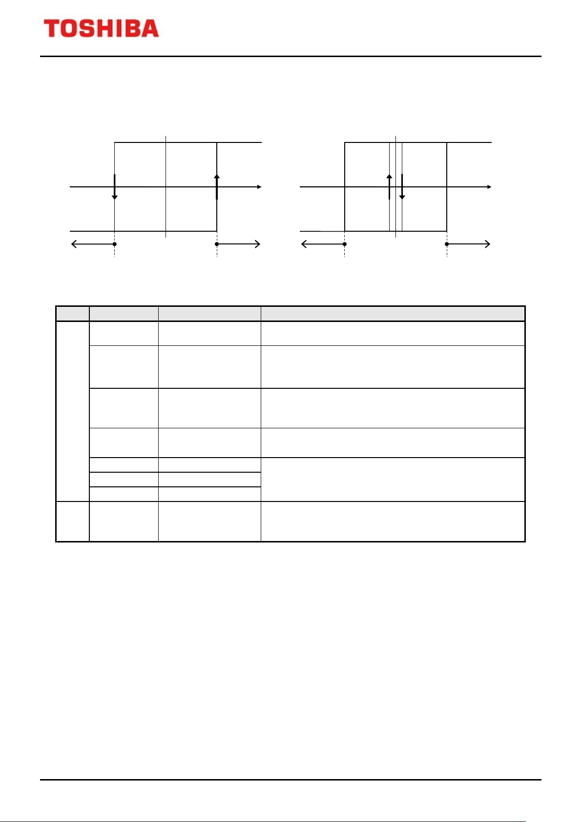
55 / 107
Positive
polarity
Negative
polarity
【 Hysteresis:HYS ≥ 0】
-HYS +HYS
【 Reverse hysteresis:HYS < 0 】
-HYS +HYS
-HYS2
+HYS2
- Stable area
+ Stable area
[ |HYS2| ≤ I, I ≤ -|HYS2|, I > HYS, I < -HYS ]
[ |HYS2| ≤ I, I ≤ -|HYS2|, I > HYS, I < -HYS ]
+ Stable area
- Stable area
Positive
polarity
Negative
polarity
Register name
Function
Detail
polarity determination
[VExIA]
[VExIB]
[VExIC]
b. Current polarity determination
TXZ/TXZ+ Family
Advanced Vector Engine Plus
Hysteresis for current
Hysteresis 2 for current
polarity determination
Dead time compensation
control/status
[15] Current polarity
determination control
a-phase current
b-phase current
c-phase current
Dead time compensation
control/status
Input
Output
[VExHYS]
[VExHYS2]
[VExDTCS]
[VExMODE]
[VExDTCS]
16-bit fixed-point data (-1.0 to 1.0, 15 fractional bits)
Polarity determination level on reverse hysteresis ([VExHYS] < 0).
16-bit fixed-point data (0 to 1.0, 15 fractional bits)
This register is invalid when [VExHYS] ≥ 0.
<ICSTS>, <IBSTS>, <IASTS>
000, 010, 100, 110: Undefined
001, 101: Positive current 011, 111: Negative current
<IPDEN>
0: Determination is disabled. 1: Determination is enabled.
32-bit fixed-point data (-1.0 to 1.0, 31 fractional bits)
<ICSTS>, <IBSTS>, <IASTS>
000, 010, 100, 110: Undefined
001, 101: Positive current 011, 111: Negative current
2021-02-24
Rev. 3.1
Page 56
TXZ/TXZ+ Family
56 / 107
Register name
Function
Detail
[VExIC]
c-phase current
Advanced Vector Engine Plus
3.3.7. Input Current Transformation (Phase Transformation/Coordinate Axis Transformation)
Input current transformation consists of two tasks: phase transformation and coordinate axis transformation.
3.3.7.1. Input phase transformation (Task 3)
Input phase transformation task calculates Iα and Iβ based on Ia, Ib, and Ic.
<Equation>
kc = 1 ; Relative transformation
if ([VExFMODE]<CCVMD> = 1) kc = √(3 / 2) ; Absolute transformation
if ([VExFMODE]<PHCVDIS> = 0) ; Phase transformation is enabled
[VExIALPHA] = kc × [VExIA] ; Calculates the value of Iα
[VExIBETA] = kc × √(1 / 3) × [VExIB] - kc × √(1 / 3) × [VExIC] ; Calculates the value of Iβ
else if ([VExFMODE]<PHCVDIS> = 1) ; Phase transformation is disabled
[VExIALPHA] = [VExIA]
[VExIBETA] = [VExIB]
Input
Output
[VExIA]
[VExFMODE]
[VExIALPHA]
[VExIBETA]
a-phase current
b-phase current
[12] Disables phase
transformation
[13] Phase
transformation mode
setting
α-axis current
β-axis current
32-bit fixed-point data (-1.0 to 1.0, 31 fractional bits) [VExIB]
<PHCVDIS>
0: 2-3 phase transformation is enabled. (3-phase AC output)
1: 2-3 phase transformation is disabled. (2-phase AC output)
<CCVMD>
0: Relative transformation
1: Absolute transformation
32-bit fixed-point data (-1.0 to 1.0, 31 fractional bits)
2021-02-24
Rev. 3.1
Page 57

TXZ/TXZ+ Family
57 / 107
Register name
Function
Detail
[VExSIN]
The sine value of θ
[VExCOS]
The cosine value of θ
[VExID]
d-axis current
[VExIQ]
Advanced Vector Engine Plus
3.3.7.2. Input coordinate axis transformation (Task 4)
In input coordinate axis transformation task, the values of [VExID] and [VExIQ] are calculated from
[VExIALFA], [VExIBETA], [VExSINM], and [VExCOSM].
a. Coordinate axis transformation
<Equation>
plslfm = [VExMCTLF]<PLSLFM>
if ([VExFMODE]<MREGDIS> = 1) ; Previous value is invalid.
plslfm = [VExMCTLF]<PLSLF>
if (plslfm = 0) ; Check the small pulse flag.
[VExID] = [VExCOSM] × [VExIALPHA] + [VExSINM] × [VExIBETA] ; Calculates the value of Id.
[VExIQ] = -[VExSINM] × [VExIALPHA] + [VExCOSM] × [VExIBETA] ; Calculates the value of Iq.
Input
Output
b. ATAN calculation
When <ATANMD> = 10, ATAN task calculates the declination angle of d-axis and q-axis current.
When <ATANMD> = 11, ATAN task calculates the induced voltage of d-axis and q-axis. Then it calculates the
declination angle using motor voltage equation based on these results.
<Equation>
if ([VExMODE]<ATANMD[1]> = 1) ; Enables calculation of the
declination angle
ld = [VExCLD] × ([VExCLG] setting) ; d-axis inductance
lq = [VExCLQ] × ([VExCLG] setting) ; q-axis inductance
r = [VExCR] × ([VExCRG] setting) ; Resistance
vdiv = [VExVD] - ([VExID] × r - [VExOMEGA] × [VExIQ] × lq) ; Induced voltage for d-axis
vqiv = [VExVQ] - ([VExIQ] × r + [VExOMEGA] × [VExID] × ld) ; Induced voltage for q-axis
[VExTMPREG3] = vdiv ; Stores d-axis induced voltage
[VExTMPREG4] = vqiv ; Stores q-axis induced voltage
if ([VExMODE]<ATANMD[0]> = 1)
[VExDELTA] = ATAN(|vqiv|, |vdiv|) ; Calculates the declination angle of
the induced voltage.
[VExIALPHA]
[VExIBETA]
[VExSINM]
[VExCOSM]
[VExFMODE]
[VExMCTLF]
α-axis current
β-axis current
Previous sine value
Previous cosine value
[9] Control for maintain
previous value
[4] PWM duty check flag
[5] Previous <PLSLF>
q-axis current
32-bit fixed-point data (-1.0 to 1.0, 31 fractional bits)
16-bit fixed-point data (-1.0 to 1.0, 15 fractional bits)
<MREGDIS>
0: Previous value is maintained.
1: Previous value is not maintained.
<PLSLF>
<PLSLFM>
32-bit fixed-point data (-1.0 to 1.0, 31 fractional bits)
2021-02-24
Rev. 3.1
Page 58
TXZ/TXZ+ Family
58 / 107
Register name
Function
Detail
[VExCLD]
[VExCLQ]
Register name
Function
Detail
[VExTMPREG4]
[VExTMPREG5]
Advanced Vector Engine Plus
else [VExDELTA] = ATAN(|[VExIQ]|, |[VExID]|) ; Calculates the declination angle of
the current
Motor d-axis inductance
Motor q-axis inductance
[VExCR]
[VExCLG] Inductance range setting 000: 1 / 1 001: 1 / 24 010: 1 / 28
[VExCRG]
Motor resistance value
VExCR range setting
16-bit fixed-point data (11 fractional bits)
011: 1 / 2
101 to 111: Reserved
12
100: 1 / 216
Input
Output
[VExOMEGA]
[VExVD]
[VExVQ]
[VExMODE]
[VExDELTA]
[VExTMPREG3]
[VExTMPREG4]
Rotational speed
d-axis voltage
q-axis voltage
[6:5] ATAN operation
mode setting
Output of the current
declination angle
d-axis induced voltage
q-axis induced voltage
16-bit fixed-point data (15 fractional bits)
32-bit fixed-point data (-1.0 to 1.0 and 31 fractional bits)
<ATANMD>
00, 01: Calculation is prohibited.
10: Calculates the declination angle for Id and Iq.
11: Calculates the declination angle of induced voltage of
d-axis and q-axis.
16-bit data (-180-degree to 180-degree)
0x8000 to 0x7FFF
16-bit fixed-point data (15 fractional bits)
3.3.8. Other Tasks
3.3.8.1. ATAN2 (Arctangent function 2) (Task 12)
ATAN2 task calculates the angle from the starting point based on X-axis that draws a straight line from the
starting point to the point of (X, Y) on the X-Y coordinate.
<Equation>
x = [VExTMPREG4]
y = [VExTMPREG5]
z = ATAN (|y|, |x|) ; Arctangent calculation (0-degree to 90-degree)
if (x < 0 & y ≥ 0) z = 0x00008000 - z ; The second quadrant (90-degree to 180-degree)
if (x < 0 & y < 0) z = 0xFFFF8000 + z ; The third quadrant (-90-degree to -180-degree)
if (x ≥ 0 & y < 0) z = -z ; The forth quadrant (0-degree to -90-degree)
if (x = y = 0) z = 0x00000000 ; Output on the original point (0-degree)
[VExTMPREG5] = z
Input
Output
[VExTMPREG5]
Input X
Input Y
The value of the phase
32-bit signed data
32-bit data (-180-degree to 180-degree)
0xFFFF8000 to 0x00008000
2021-02-24
Rev. 3.1
Page 59
TXZ/TXZ+ Family
59 / 107
Register name
Function
Detail
Advanced Vector Engine Plus
3.3.8.2. SQRT (Square root function) (Task 13)
SQRT task outputs the value from 0.0 to 2.0 based on the calculation of the square root function using the inputs
from 0.0 to 4.0.
<Equation>
x = [VExTMPREG5] ; Input (0 to 4.0)
n = 0
if (x < 0x2000) n = 1
if (x < 0x0800) n = 2
if (x < 0x0200) n = 3
if (x < 0x0080) n = 4
if (x < 0x0020) n = 5
if (x < 0x0008) n = 6
if (x < 0x0002) n = 7
if (x < 0x8000) n = -1
x = x × 2
if (x ≥ 0x7FFF) x = 0x7FFF
z = SQRT(x) ; Calculates the square root of x,
; Output is the range of 0.5 to 1.0
if (x = 0) z = 0
z = z / 2
[VExTMPREG5] = z
2n
; Normalization (0.25 to 1.0)
n
; Inverted transformation (0 to 2.0)
[VExTMPREG5]
Input
Output
[VExTMPREG5]
Input value
The value of square root
32-bit fixed-point data (0.0 to 4.0, 15 fractional bits)
0x00000000 to 0x0001FFFF
32-bit fixed-point data (0.0 to 2.0, 15 fractional bits)
0x00000000 to 0x0000FFFF
2021-02-24
Rev. 3.1
Page 60
60 / 107
Register Name
Address (Base+)
[VExEN]
[VExCPURUNTRG]
Task Selection Register
[VExTASKAPP]
0x0008
[VExSCHTASKRUN]
[VExTMPREG0]
[VExTMPREG1]
0x0030
4. Registers
The vector engine has the VE control registers and the dedicated registers.
● VE control registers
The vector engine control registers and temporary registers.
● Dedicated registers
Computation data registers and computation control registers.
Note: Use word access (32 bits) to the registers.
4.1. List of Registers
The control registers and their addresses are shown as follows:
TXZ/TXZ+ Family
Advanced Vector Engine Plus
Peripheral Function Channel/Unit
TYPE1 TYPE2 TYPE3
Advanced Vector Engine plus A-VE+ ch0 0x400F8000 0x400EB000 0x4008B000
Base address
Note: The Channel/Unit and Base address type are different by products. Please refer to "Product Information"
of the reference manual for the details.
VE control register
VE Operation Enable/Disable Register
CPU Start Trigger Selection Register
Operation Schedule Selection Register
Operation Schedule Repeat Number Selection Register [VExREPTIME]
Start Trigger Mode Setting Register [VExTRGMODE]
Error Interrupt Enable/Disable Setting Register
VE Forcible Termination Register
Error Detection Register
Schedule Operation Status/Ongoing Task Number Register
Temporary Register 0
Temporary Register 1
Temporary Register 2
Temporary Register 3
Temporary Register 4
Temporary Register 5
[VExACTSCH]
[VExERRINTEN]
[VExCOMPEND]
[VExERRDET]
[VExTMPREG2]
[VExTMPREG3]
[VExTMPREG4]
[VExTMPREG5]
0x0000
0x0004
0x000C
0x0010
0x0014
0x0018
0x001C
0x0020
0x0024
0x002C
0x0034
0x0038
0x003C
0x0040
2021-02-24
Rev. 3.1
Page 61
61 / 107
Register Name
Address (Base+)
[VExMCTLF]
[VExMODE]
[VExFMODE]
0x004C
[VExCIDKI]
[VExCIDKP]
[VExCIQKI]
[VExFPWMCHG]
[VExPWMOFS]
0x0090
[VExCOSM]
[VExSINM]
[VExSECTOR]
[VExSECTORM]
a-phase Zero-Current Register
[VExIAO]
0x00B8
[VExID]
[VExIQ]
[VExTADC]
U-phase PWM Duty Register
[VExCMPU]
0x017C
Dedicated registers
TXZ/TXZ+ Family
Advanced Vector Engine Plus
Status Register
Task Control Mode Register
Flow Control Register
PWM Period Rate setting Register
Rotational Speed setting Register
Motor Phase setting Register
d-axis Current Reference setting Register
q-axis Current Reference setting Register [VExIQREF]
d-axis Voltage setting Register [VExVD]
q-axis Voltage setting Register
d-axis Current Integral Coefficient setting Register for PI control
d-axis Current Proportional Coefficient setting Register for PI control
q-axis Current Integral Coefficient setting Register for PI control
q-axis Current Proportional Coefficient setting Register for PI control [VExCIQKP]
d-axis Voltage Integral component Store Register for PI control
(Upper)
d-axis Voltage Integral component Store Register for PI control
(Lower)
q-axis Voltage Integral component Store Register for PI control
(Upper)
q-axis Voltage Integral component Store Register for PI control
(Lower)
PWM Switching Speed setting Register
PWM Shift 2 Offset Register
Minimum Pulse Width setting Register
Synchronous Trigger Correction setting Register
DC2 Supply Voltage Register
Cosine value Register of θ
Sine value Register of θ [VExSIN]
Previous Cosine value Register
Previous Sine value Register
Sector Information Register
Previous Sector Information Register
[VExTPWM]
[VExOMEGA]
[VExTHETA]
[VExIDREF]
[VExVQ]
[VExVDIH]
[VExVDILH]
[VExVQIH]
[VExVQILH]
[VExMINPLS]
[VExTRGCRC]
[VExVDCL]
[VExCOS]
0x0044
0x0048
0x0050
0x0054
0x0058
0x005C
0x0060
0x0064
0x0068
0x006C
0x0070
0x0074
0x0078
0x007C
0x0080
0x0084
0x0088
0x008C
0x0094
0x0098
0x009C
0x00A0
0x00A4
0x00A8
0x00AC
0x00B0
0x00B4
b-phase Zero-Current Register [VExIBO]
c-phase Zero-Current Register [VExICO]
ADC Conversion Result Register for a-phase Current
ADC Conversion Result Register for b-phase Current
ADC Conversion Result Register for c-phase Current
DC Supply Voltage Register
d-axis Current Register
q-axis Current Register
ADC Conversion Time setting Register
V-phase PWM Duty Register
[VExIAADC]
[VExIBADC]
[VExICADC]
[VExVDC]
[VExCMPV]
0x00BC
0x00C0
0x00C4
0x00C8
0x00CC
0x00D0
0x00D4
0x00D8
0x0178
0x0180
2021-02-24
Rev. 3.1
Page 62
62 / 107
Register Name
Address (Base+)
[VExOUTCR]
[VExTRGCMP0]
PMD Trigger 1 Timing setting Register
[VExTRGCMP1]
0x0190
[VExVDQ]
[VExDELTA]
[VExCPHI]
[VExCLD]
[VExVQE]
[VExDTC]
[VExHYS]
[VExDTCS]
PWM Upper-Limit setting Register
[VExPWMMAX]
0x0204
[VExVDUTYB]
[VExVDUTYC]
[VExIALPHA]
0x0228
TXZ/TXZ+ Family
Advanced Vector Engine Plus
W-phase PWM Duty Register
PMD Output Control Register
PMD Trigger 0 Timing setting Register
Synchronous Trigger Selection setting Register [VExTRGSEL]
EMG release Register
Output Limitation Register for PI control
d-axis Coefficient Range setting Register for PI control
q-axis Coefficient Range setting Register for PI control
Voltage Scalar Limitation Register [VExVSLIM]
Voltage Scalar Register
Current Declination Angle Register
Motor Interlinkage Magnetic Flux Register
Motor q-axis Inductance Constant Register
Motor d-axis Inductance Constant Register
Motor Resistance Constant Register [VExCR]
Motor Magnetic Flux Range setting Register [VExCPHIG]
Motor Inductance Range setting Register
Motor Resistance Range setting Register
d-axis Voltage Register for Non-interference Control
q-axis Voltage Register for Non-interference Control
Dead Time Compensation Register
Hysteresis Width Register for Current Polarity Determination
Dead Time Compensation Control/Status Register
[VExCMPW]
[VExEMGRS]
[VExPIOLIM]
[VExCIDKG]
[VExCIQKG]
[VExCLQ]
[VExCLG]
[VExCRG]
[VExVDE]
0x0184
0x0188
0x018C
0x0194
0x0198
0x01BC
0x01C0
0x01C4
0x01C8
0x01CC
0x01D0
0x01D4
0x01D8
0x01DC
0x01E0
0x01E4
0x01E8
0x01EC
0x01F0
0x01F4
0x01F8
0x01FC
0x0200
PWM Lower-Limit setting Register
Clipped Phase value setting Register
Hysteresis Width Register 2 for Current Polarity Determination [VExHYS2]
α-phase Voltage Register
β-phase Voltage Register
a-phase Voltage Duty Register
b-phase Voltage Duty Register
c-phase Voltage Duty Register
α-phase Current Register
β-phase Current Register
a-phase Current Register
b-phase Current Register
c-phase Current Register
Voltage declination angle Register [VExVDELTA]
d-axis Voltage correction Register [VExVDCRC]
q-axis Voltage correction Register
[VExPWMMIN]
[VExTHTCLP]
[VExVALPHA]
[VExVBETA]
[VExVDUTYA]
[VExIBETA]
[VExVQCRC]
[VExIA]
[VExIB]
[VExIC]
0x0208
0x020C
0x0210
0x0214
0x0218
0x021C
0x0220
0x0224
0x022C
0x0230
0x0234
0x0238
0x023C
0x0240
0x0244
2021-02-24
Rev. 3.1
Page 63
63 / 107
After
Reset
After
Reset
4.2. Details of VE Control Registers
4.2.1. [VExEN] (VE Operation Enable/Disable Register)
TXZ/TXZ+ Family
Advanced Vector Engine Plus
Bit Bit Symbol
31:2 - 0 R
1 - 0 R/W
0 VEEN 0 R/W
Type Function
Read as "0"
Write as "0"
Selects the VE operation.
0: Disabled
1: Enabled
Note1: When the VE is disabled (<VEEN> = 0), access to other registers of the VE is not allowed
Note2: To change the PMD registers from VE, be sure to set the operation schedule repetition count
specification register [VExREPTIME]<VREP> to other than "0x0" after enabling the VE operation
(<VEEN> = 1).
4.2.2. [VExCPURUNTRG] (CPU Start Trigger Selection Register)
Bit Bit Symbol
31:1 - 0 R Read as "0"
0 VCPURT 0 W
Note 1: When "1" is written to this bit, it is cleared on the next cycle. This bit always read as "0".
Note 2: If new schedules and the tasks start operation while another schedule is being executed, the vector
engine should be terminated with the [VExCOMPEND] register before it is started with the
[VExCPURUNTRG] register again.
Type Function
Starts the vector engine by software.
0: 1: Starts operation
Operation starts from the task configured to [VExTASKAPP]
<VTASK>.
Specify [VExTASKAPP], [VExACTSCH], and [VExREPTIME]
before starting operation.
2021-02-24
Rev. 3.1
Page 64
64 / 107
After
Reset
4.2.3. [VExTASKAPP] (Task Selection Register)
TXZ/TXZ+ Family
Advanced Vector Engine Plus
Bit Bit Symbol
31:12 - 0 R Read as "0"
11:8 VITASK[3:0] 0x0 R/W
7:4 - 0 R
3:0 VTASK[3:0] 0x0 R/W
Type Function
Selects the timing at which the task end interrupt occurs.
0x0: Output control 1 (Task 0)
0x1: Trigger generation (Task 1)
0x2: Input process 1 (Task 2)
0x3: Input phase transformation (Task 3)
0x4: Input coordinate axis transformation (Task 4)
0x5: Current control (Task 5)
0x6: SIN/COS calculation (Task 6)
0x7: Output coordinate axis transformation (Task 7)
0x8: Output phase transformation 1[SVM] (Task 8)
0x9: Output control 2 (Task 9)
0xA: Input process 2 (Task 10)
0xB: Output phase transformation 2[I-Clarke] (Task 11)
0xC: ATAN2 (Task 12)
0xD: SQRT (Task 13)
0xE, 0xF: Reserved
Read as "0"
Selects the start task.
0x0: Output control 1 (Task 0)
0x1: Trigger generation (Task 1)
0x2: Input process 1 (Task 2)
0x3: Input phase transformation (Task 3)
0x4: Input coordinate axis transformation (Task 4)
0x5: Current control (Task 5)
0x6: SIN/COS calculation (Task 6)
0x7: Output coordinate axis transformation (Task 7)
0x8: Output phase transformation 1[SVM] (Task 8)
0x9: Output control 2 (Task 9)
0xA: Input process 2 (Task 10)
0xB: Output phase transformation 2[I-Clarke] (Task 11)
0xC: ATAN2 (Task 12)
0xD: SQRT (Task 13)
0xE, 0xF: Reserved
Selects the task that is started by software.
Note: Only those tasks that are included in the schedules can be specified.
2021-02-24
Rev. 3.1
Page 65
65 / 107
After
Reset
After
Reset
After
Reset
4.2.4. [VExACTSCH] (Operation Schedule Selection Register)
TXZ/TXZ+ Family
Advanced Vector Engine Plus
Bit Bit Symbol
31:4 - 0 R Read as "0"
3:0 VACT[3:0] 0x0 R/W
Type Function
Selects individual task execution or an operation schedule.
0x0: Executes individual task.
0x1: Schedule 1
0x2: Schedule 2
0x3: Schedule 3
0x4: Schedule 4
0x5: Schedule 5
0x6: Schedule 6
0x7: Schedule 7
0x8: Schedule 8
0x9: Schedule 9
0xA: Schedule 10
0xB: Schedule 11
0xC: Schedule 12
0xD: Schedule 13
0xE: Schedule 14
0xF: Schedule 15
For details, refer to "Table 3.1 Execution task in each schedule".
4.2.5. [VExREPTIME] (Operation Schedule Repeat Number Selection Register)
Bit Bit Symbol
31:4 - 0 R
3:0 VREP[3:0] 0x0 R/W
Type Function
Read as "0"
Selects the number of repeat of the operation schedule.
0x0: No schedule operation is performed.
0x1 to 0xF: Repeats the specified number of times of the
schedule operation
Note: When this bit is set to "0x0", do not start schedule operation.
4.2.6. [VExTRGMODE] (Start Trigger Mode Setting Register)
Bit Bit Symbol
31:2 - 0 R
1:0 VTRG[1:0] 00 R/W
Note: Connection varies depending on the product. Refer to "Product Information".
Type Function
Read as "0"
Selects the input process start condition using an ADC conversion
end interrupt.
00: Reserved
01: Input process is started by a INTADxPDA (ADC conversion
end interrupt A).(Note)
10: Input process is started by a INTADxPDB (ADC conversion
end interrupt B).(Note)
11: Reserved
2021-02-24
Rev. 3.1
Page 66
Advanced Vector Engine Plus
66 / 107
After
Reset
If a PWM interrupt is detected when an operation schedule is being
is set as an
After
Reset
After
Reset
4.2.7. [VExERRINTEN] (Error Interrupt Enable/Disable Setting Register)
TXZ/TXZ+ Family
Bit Bit Symbol
31:3 - 0 R Read as "0"
2 INTTEN 0 R/W
1 - 0 R
0 VERREN 0 R/W
Type Function
Controls a task end interrupt.
0: Disabled
1: Enabled
Read as "0"
Controls an interrupt at error detection.
0: Disabled
1: Enabled
executed (an activation trigger wait is not included), "1"
error flag.
4.2.8. [VExCOMPEND] (VE Forcible Termination Register)
Bit Bit Symbol
31:1 - 0 R Read as "0"
0 VCEND 0 W
Type Function
Ongoing schedule is forcibly terminated.
0: 1: Stop
If "1" is written to this bit, this bit is cleared on next cycle. Always
read as "0"
4.2.9. [VExERRDET] (Error Detection Register)
Bit Bit Symbol
31:1 - 0 R
0 VERRD 0 R
Type Function
Read as "0"
This bit indicates the error flag.
0: An error is not detected.
1: An error is detected.
When an operation schedule is being executed (excluding a start
trigger wait), if a PW M interrupt is detected, "1" is set to this bit.
This bit is cleared upon read.
2021-02-24
Rev. 3.1
Page 67
TXZ/TXZ+ Family
67 / 107
After
Reset
After
Reset
[31:0]
Advanced Vector Engine Plus
4.2.10. [VExSCHTASKRUN] (Schedule Operation Status/Ongoing Task Number Register)
Bit Bit Symbol
31:5 - 0 R Read as "0"
4:1 VRTASK[3:0] 0x0 R
0 VRSCH 0 R
Type Function
Indicates the ongoing task number.
0x0: Output control 1 (Task 0)
0x1: Trigger generation (Task 1)
0x2: Input process 1 (Task 2)
0x3: Input phase transformation (Task 3)
0x4: Input coordinate axis transformation (Task 4)
0x5: Current control (Task 5)
0x6: SIN/COS calculation (Task 6)
0x7: Output coordinate axis transformation (Task 7)
0x8: Output phase transformation 1[SVM] (Task 8)
0x9: Output control 2 (Task 9)
0xA: Input process 2 (Task 10)
0xB: Output phase transformation 2[I-Clarke] (Task 11)
0xC: ATAN2 (Task 12)
0xD: SQRT (Task 13)
0xE, 0xF: Reserved
Indicates schedule execution status.
0: Stop
1: Being executed
4.2.11. [VExTMPREG0] (Temporary Registers 0)
Example of [VExTMPREG0]. [VExTMPREG1] to [VExTMPREG5] have the same configuration.
Bit Bit Symbol
31:0
TMPREG0
0x00000000 R/W
Type Function
Temporary register 0
2021-02-24
Rev. 3.1
Page 68
68 / 107
After
Reset
This bit is updated when output phase transformations (Task 8 and 11)
4.3. Details of Dedicated Registers
4.3.1. [VExMCTLF] (Status Register)
TXZ/TXZ+ Family
Advanced Vector Engine Plus
Bit Bit Symbol
31:16 - 0 R
15 SFT2STM 0 R/W
14 SFT2ST 0 R/W
13:12 - 00 R/W Write as "00"
11 PWMOVF 0 R/W
10 VSOVF 0 R/W
9 PIQOVF 0 R/W
Type Function
Read as "0"
Previous value of <SFT2ST>
The value is updated when output control 2 (Task 9) is executed.
A PWM carrier reverse flag of PWM Shift 2
The value is updated when output control 2 (Task 9) is executed.
0: Without PW M carrier reverse of reference phase
1: With PWM carrier reverse of reference phase
Set "1" to this bit when Shift 2 reference phase duty < 0x4000
Indicates the excess flag for PWM output limitation.
0: All 3-phase PWM outputs are [VExPWMMIN] or more, and
[VExPWMMAX] or less.
1: Any 3-phase PWM outputs are less than [VExPWMMIN], or
over [VExPWMMAX].
This bit is updated when output controls (Task 0 and Task 9) are
executed.
Indicates the excess flag for voltage scalar limitation.
0: Voltage scalar ≤ [VExVSLIM]
1: Voltage scalar > [VExVSLIM]
This bit is updated when current control (Task 5) is executed.
Indicates the excess flag for q-axis output limitation on PI control.
0: |q-axis output on PI control | ≤ [VExPIOLIM]
1: |q-axis output on PI control | > [VExPIOLIM]
This bit is updated when current control (Task 5) is executed.
Indicates the excess flag for d-axis output limitation on PI control.
8 PIDOVF 0 R/W
7:6 - 00 R/W Write as "00"
5 PLSLFM 0 R/W
4 PLSLF 0 R/W
3 - 0 R/W Write as "0"
2 LVTF 0 R/W
0: |d-axis output on PI control | ≤ [VExPIOLIM]
1: |d-axis output on PI control | > [VExPIOLIM]
This bit is updated when current control (Task 5) is executed.
Indicates the previous value of the <PLSLF> register.
This bit is updated when output controls (Task 0 and Task 9) are
executed.
PWM duty check flag.
This bit is updated when output controls (Task 0 and Task 9) are
executed.
When output control 1(Task 0) is executed and 1-shunt current
detection is set,
0: [VExMINPLS] ≤ Difference of minimum pulse width
1: [VExMINPLS] > Difference of minimum pulse width
When output control 2 (Task 9) is executed,
0: [VExMINPLS] ≤ Minimum On-width or minimum Off-width
1: [VExMINPLS] > Minimum On-width or minimum Off-width
Low supply voltage flag
0: [VExVDC] ≥ 1 / 128 (0x0100)
1: [VExVDC] < 1 / 128 (0x0100)
are executed.
2021-02-24
Rev. 3.1
Page 69
TXZ/TXZ+ Family
69 / 107
After
Reset
After
Reset
Advanced Vector Engine Plus
Bit Bit Symbol
1 LAVFM 0 R/W
0 LAVF 0 R/W
Type Function
Previous value of the <LAVF> register
This bit is updated when output controls (Task 0 and Task 9) are
executed.
Low-speed flag
This bit is updated when output controls (Task 0 and Task 9) are
executed.
0: High speed ([VExOMEGA] ≥ [VExFPWMCHG])
1: Low speed ([VExOMEGA] < [VExFPWMCHG])
4.3.2. [VExMODE] (Task Control Mode Register)
Bit Bit Symbol
31:16 - 0 R
15 IPDEN 0 R/W
14 PMDDTCEN 0 R/W
Type Function
Read as "0"
Disables/enables current polarity determination for Task 2 and Task 10.
0: Disabled
1: Enabled
Refer to "3.3.6 Input Process".
Setting that corresponds to the dead time correction control of the PMD
when the dead time compensation for Task 0 and Task 9 is performed.
0: Dead time correction of the PMD is disabled.
1: Dead time correction of the PMD is enabled.
Refer to "3.3.4 Output Control".
13 PWMFLEN 0 R/W
12 PWMBLEN 0 R/W
11 NICEN 0 R/W
10 T5ECEN 0 R/W
9:8 AWUMD[1:0] 00 R/W
Disables/enables a duty of 100% setting when the upper-limit for Task 0
and Task 9 is set.
0: Duty of 100% setting is disabled.
1: Duty of 100% setting is enabled.
Refer to "3.3.4 Output Control".
Disables/enables a duty of 0% setting when the lower-limit for Task 0
and Task 9 is set.
0: Duty of 0% setting is disabled.
1: Duty of 0% setting is enabled.
Refer to "3.3.4 Output Control".
Disables/enables Non-interference control for Task 5.
0: Disabled
1: Enabled
Refer to "3.3.1 Current Control (Task 5)".
Disables/enables expansion control (Non-interference control and
voltage scalar limitation) for Task 5.
0: Disabled
1: Enabled
Refer to "3.3.1 Current Control (Task 5)".
Specifies anti-windup (AWU) control for Task 5 when PI control output
limitation is performed.
00: AWU control is disabled.
01: Substitutes the result from amount of limitation / 4
into the integral term.
10: Substitutes the result from amount of limitation / 2
into the integral term.
11: Substitutes the amount of limitation into the integral term.
Refer to "3.3.1 Current Control (Task 5)".
2021-02-24
Rev. 3.1
Page 70
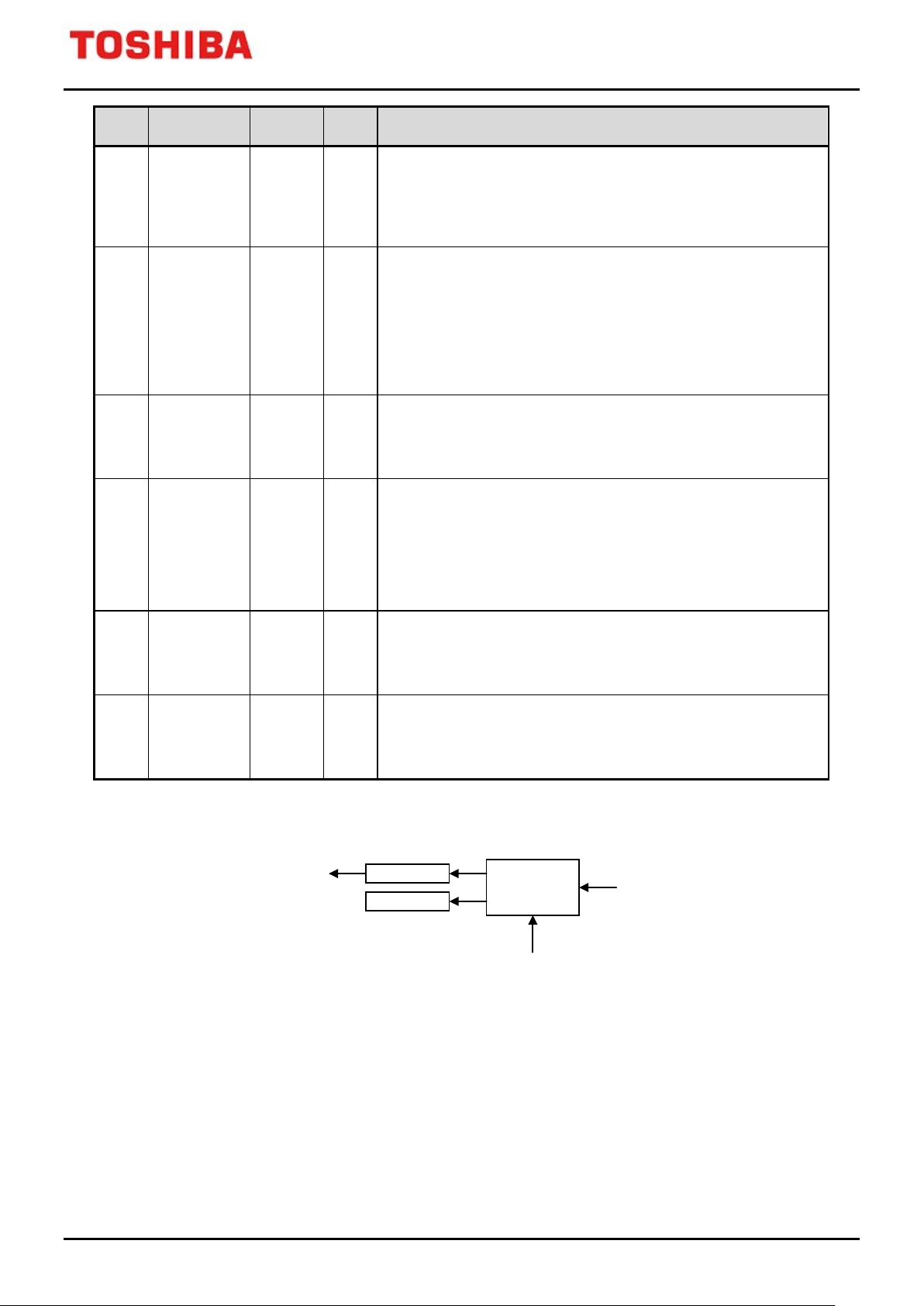
TXZ/TXZ+ Family
70 / 107
After
Reset
Selector
[VExVDC]
[VExVDCL]
[VExMODE]
<VDCSEL>
Input process
(ADC)
Output phase transformation
(Tas k 8 and 11)
Advanced Vector Engine Plus
Bit Bit Symbol
7 CLPEN 0 R/W
6:5
4 VDCSEL 0 R/W
3:2 OCRMD[1:0] 00 R/W
ATANMD
[1:0]
00 R/W
Type Function
Disables/enables phase clipping control for Task 6 when phase
interpolation is performed.
0: Clipping is disabled.
1: Clipping is enabled.
Refer to "3.3.2 SIN/COS calculation (Task 6)".
Specifies ATAN calculation control for Task 4.
00, 01: Calculation is disabled.
10: Calculates the declination angle on d-q coordinate of
current vector.
11: Calculates the declination angle on d-q coordinate of
induced voltage vector.
Refer to "3.3.7 Input Current Transformation (Phase
Transformation/Coordinate Axis Transformation)".
Selects the supply voltage store register for Task 2 and Task 10.
0: Stored in [VExVDC].
1: Stored in [VExVDCL].
Refer to Figure 4.1.
Specifies output control for Task 0 and Task 9.
00: Output is disabled.
01: Output is enabled.
10: Short circuit brake (Outputs are OFF in the upper-phase;
outputs are ON in the lower-phase.)
11: EMG release (Outputs are OFF.)
Refer to "3.3.4 Output Control".
1 ZIEN 0 R/W
0 PVIEN 0 R/W
Note: When a power supply voltage controlled by [VExVDC] register is corrected, select [VExVDCL] register
as a storage location, and set a corrected value in [VExDVC] register.
Figure 4.1 [VExVDC]/[VExVDCL] store register
Specifies zero-current detection control for Task 2.
0: Normal current detection
1: Zero-current detection
Refer to "3.3.6 Input Process".
Disables/enables phase interpolation control for Task 6.
0: Disabled
1: Enabled
Refer to "3.3.2 SIN/COS calculation (Task 6)".
2021-02-24
Rev. 3.1
Page 71
71 / 107
After
Reset
Phase transformation cannot be disabled when space vector modulation
4.3.3. [VExFMODE] (Flow Control Register)
TXZ/TXZ+ Family
Advanced Vector Engine Plus
Bit Bit Symbol
31:16 - 0 R Read as "0"
15:14 SPWMMD[1:0] 00 R/W
13 CCVMD 0 R/W
12 PHCVDIS 0 R/W
11:10 VSLIMMD[1:0] 00 R/W
Type Function
Selects a PWM Shift mode.
00: Shift 1
01: Shift 2 (U-phase Center PWM)
10: Shift 2 (V-phase Center PWM)
11: Shift 2 (W-phase Center PWM)
Shift 2 cannot be selected when output control 1 (Task 0) is being
executed (invalid).
Selects a phase transformation mode.
0: Relative transformation
1: Absolute transformation
Disables/enables phase transformation.
0: 2-3 phase transformation is enabled. (3-phase AC output)
1: 2-3 phase transformation is disabled. (2-phase AC output)
(Task 8) is running (invalid).
Controls voltage scalar limitation of current control (Task 5).
00: Scalar limitation is disabled.
(The limitation of each axis is enabled.)
01: Limits the voltage on the d-axis.
10: Limits the voltage on the q-axis.
11: dq proportional limitation
9 MREGDIS 0 R/W
8 CRCEN 0 R/W
7 ICPLMD 0 R/W
6 IBPLMD 0 R/W
5 IAPLMD 0 R/W
4 IDQSEL 0 R/W
Enables/Disables the use of previous value flags of MCTLF, SIN, COS,
and SECTOR registers on the input process 1, 2, and on input
coordinate transformation.
0: Enabled
1: Disabled
Disables/enables trigger correction
0: Disabled
1: Enabled
This bit is enabled when trigger generation (Task 1) is being executed;
when PWM Shift is disabled in 1-shunt current detection mode; or when
Shift 1 is selected.
Selects the current direction ([VExIC]) of input process2 (Task 10).
0: Shunt mode ([VExIC] = [VExICO] – [VExICADC])
1: Sensor mode ([VExIC] = [VExICADC] – [VExICO])
Selects the current direction ([VExIB]) of input process2 (Task 10).
0: Shunt mode ([VExIB] = [VExIBO] – [VExIBADC])
1: Sensor mode ([VExIB] = [VExIBADC] – [VExIBO])
Selects the current direction ([VExIA]) of input process2 (Task 10).
0: Shunt mode ([VExIA] = [VExIAO] – [VExIAADC])
1: Sensor mode ([VExIA] = [VExIAADC] – [VExIAO])
Selects Non-interference control input current
0: Feedback current ([VExID], [VExIQ])
1: Command current ([VExIDREF], [VExIQREF])
2021-02-24
Rev. 3.1
Page 72
TXZ/TXZ+ Family
72 / 107
After
Reset
PWM Shift 2 should be used when output control 2 (Task 9) and
input process 1 (Task 2) are available only
in Shift 1 mode. Output control 2 (Task 9) and input process 2 (Task 10)
After
Reset
After
Reset
Advanced Vector Engine Plus
Bit Bit Symbol
3:2 IDMODE[1:0] 00 R/W
1 SPWMEN 0 R/W
0 C2PEN 0 R/W
Type Function
Selects current detection mode.
00: 3-shunt (Note 1)
01: 2-sensor (Note 2)
10: 1-shunt (PMD TRG in the latter half of PWM(Note 3))
11: 1-shunt (PMD TRG in the first half of PW M(Note 3))
Note 1: 3-phase current detection is used in input process 2 (Task 10).
Note 2: 2-phase current detection is used in input process 2 (Task 10).
Note 3:
input process 2 (Task 10) is being executed.
Disables/enables PWM Shift.
0: Disabled
1: Enabled
Output control 1 (Task 0) and
are available only in Shift 2 mode.
Selects the modulation mode.
0: 3-phase modulation
1: 2-phase modulation
4.3.4. [VExTPWM] (PWM Period Rate setting Register)
Bit Bit Symbol
31:16 - 0 R Read as "0"
15:0 TPWM[15:0] 0x0000 R/W
Type Function
Sets the PWM period rate and the unit of integration in phase
interpolation (16-bit fixed-point data: 0.0 to 1.0).
0x0000 to 0xFFFF (PWM period[s] × Max_Hz × 216)
This indicates the ratio between PWM period and the maximum
rotational speed. (Max_Hz: Maximum rotational speed)
This bit is used for SIN/COS calculation (Task 6) when phase
interpolation is enabled.
4.3.5. [VExOMEGA] (Rotational Speed setting Register)
Bit Bit Symbol
31:16 - 0 R Read as "0"
15:0 OMEGA[15:0] 0x0000 R/W
Type Function
Sets a rotational speed (16-bit fixed-point data: -1.0 to 1.0).
0x8000 to 0x7FFF: Rotational speed [Hz] / Max_Hz × 215
(Max_Hz: Maximum rotational speed)
This bit is used for SIN/COS calculation (Task 6) when phase
interpolation is enabled.
This bit is used for output control 1 (Task 0) when PWM Shift 1 is
selected for 1-shunt current detection.
This bit is used for current control (Task 5) and input coordinate axis
transformation (Task 4) in motor voltage equation.
2021-02-24
Rev. 3.1
Page 73
73 / 107
After
Reset
This bit is updated when SIN/COS calculation (Task 6) is executed
After
Reset
After
Reset
4.3.6. [VExTHETA] (Motor Phase setting Register)
TXZ/TXZ+ Family
Advanced Vector Engine Plus
Bit Bit Symbol
31:16 - 0 R Read as "0"
15:0 THETA[15:0] 0x0000 R/W
Type Function
Sets the phase (16-bit fixed-point data: 0.0 to 1.0).
0x0000 to 0xFFFF: Phase [deg] / 360 × 2
This bit is used for SIN/COS calculation (Task 6) when phase
interpolation is enabled.
while phase interpolation is enabled.
4.3.7. d-axis/q-axis Current Reference setting Registers
4.3.7.1. [VExIDREF] (d-axis Current Reference setting Register)
Bit Bit Symbol
31:16 - 0 R
15:0 IDREF[15:0] 0x0000 R/W
Type Function
Read as "0"
Sets the reference value of d-axis current (16-bit fixed-point data:
-1.0 to 1.0).
0x8000 to 0x7FFF: d-axis current reference [A] / Max_I × 215
Max_I: (The amount of phase current variation when the AD
conversion is changed by 1LSB [A]) × 211
This bit is used for current control (Task 5).
16
4.3.7.2. [VExIQREF] (q-axis Current Reference setting Register)
Bit Bit Symbol
31:16 - 0 R
15:0 IQREF[15:0] 0x0000 R/W
Type Function
Read as "0"
Sets the reference value of q-axis current (16-bit fixed-point data:
-1.0 to 1.0).
0x8000 to 0x7FFF: q-axis current reference [A] / Max_I × 2
Max_I: (The amount of phase current variation when the AD
conversion is changed by 1LSB [A]) × 2
This bit is used for current control (Task 5).
15
11
2021-02-24
Rev. 3.1
Page 74
74 / 107
After
Reset
After
Reset
After
Reset
when direction scalar
4.3.8. d-axis/q-axis Voltage setting Registers
4.3.8.1. [VExVD] (d-axis Voltage setting Register)
TXZ/TXZ+ Family
Advanced Vector Engine Plus
Bit Bit Symbol
31:0 VD[31:0] 0x00000000 R/W
Type Function
Sets the value of d-axis voltage (32-bit fixed-point data: -1.0 to
1.0).
0x80000000 to 0x7FFFFFFF: d-axis voltage[V] / Max_V × 2
Max_V: (The amount of supply voltage variation when the AD
conversion is changed by 1LSB [V]) × 212
This bit is updated when current control (Task 5) is executed.
This bit is used for output coordinate axis transformation (Task 7).
This bit is used for input coordinate axis transformation (Task 4) in
motor voltage equation.
4.3.8.2. [VExVQ] (q-axis Voltage setting Register)
Bit Bit Symbol
31:0 VQ[31:0] 0x00000000 R/W
Type Function
Sets the value of q-axis voltage (32-bit fixed-point data: -1.0 to
1.0).
0x80000000 to 0x7FFFFFFF: q-axis voltage[V] / Max_V × 2
Max_V: (The amount of supply voltage variation when the AD
conversion is changed by 1LSB [V]) × 212
This bit is updated when current control (Task 5) is executed.
This bit is used for output coordinate axis transformation (Task 7).
This bit is used for input coordinate axis transformation (Task 4) in
motor voltage equation.
31
31
4.3.8.3. [VExVDQ] (Voltage Scalar Register)
Bit Bit Symbol
31:16 - 0 R
15:0 VDQ[15:0] 0x0000 R/W
Type Function
Read as "0"
Sets value of voltage scalar for d-axis voltage [VExVD] and q-axis
voltage [VExVQ], or sets the limitation value of axis for d-axis
voltage [VExVD] and q-axis voltage [VExVQ]
is limited.
0x0000 to 0x7FFF: Voltage [V] / Max_V × 215
Max_V: (The amount of supply voltage variation when the AD
This bit is updated for current control (Task 5) when expansion
control is enabled.
conversion is changed by 1LSB [V]) × 2
12
2021-02-24
Rev. 3.1
Page 75

75 / 107
After
Reset
(Task 5) when expansion control is
4.3.8.4. [VExVSLIM] (Voltage Scalar Limitation Register)
TXZ/TXZ+ Family
Advanced Vector Engine Plus
Bit Bit Symbol
31:16 - 0 R Read as "0"
15:0 VSLIM[15:0] 0x0000 R/W
Type Function
Sets the limitation value of voltage scalar for d-axis voltage [VExVD]
and q-axis voltage [VExVQ].
0x0000 to 0x7FFF: Voltage [V] / Max_V × 2
Max_V: (The amount of supply voltage variation when the AD
Limitation of scalar voltage is not effective when "0x0000" is set.
This bit is used for current control
enabled.
15
conversion is changed by 1LSB [V]) × 2
12
2021-02-24
Rev. 3.1
Page 76
TXZ/TXZ+ Family
76 / 107
After
Reset
After
Reset
After
Reset
Advanced Vector Engine Plus
4.3.9. Coefficient Registers for PI control
4.3.9.1. [VExCIDKI] (d-axis Current Integral Coefficient setting Register for PI control)
Bit Bit Symbol
31:16 - 0 R Read as "0"
15:0 CIDKI[15:0] 0x0000 R/W
Type Function
Sets the PI control integral coefficient for d-axis.
0x8000 to 0x7FFF
4.3.9.2. [VExCIDKP] (d-axis Current Proportional Coefficient setting Register for PI
control)
Bit Bit Symbol
31:16 - 0 R
15:0 CIDKP[15:0] 0x0000 R/W
Type Function
Read as "0"
Sets the PI control proportional coefficient for d-axis.
0x8000 to 0x7FFF
4.3.9.3. [VExCIDKG] (d-axis Coefficient Range setting Register for PI control)
Bit Bit Symbol
Type Function
31:16 - 0 R
15:8 CIDKPG[7:0] 0x00 R/W
7:0 CIDKIG[7:0] 0x00 R/W
Read as "0"
Selects a PI control d-axis proportional coefficient range.
0x00: 1 / 1
0x01: 1 / 2
0x02: 1 / 2
0x03: 1 / 212
0x04: 1 / 2
0x05 to 0x08: Reserved
0x09: 2
0x0A: 2
0x0B: 2
0x0C: 2
0x0D to 0xFF: Reserved
This bit is used for current control (Task 5).
Selects a PI control d-axis integral coefficient range.
0x00: 1 / 1
0x01: 1 / 2
0x02: 1 / 28
0x03: 1 / 2
0x04: 1 / 2
0x05 to 0xFF: Reserved
This bit is used for current control (Task 5).
4
8
16
2
3
4
4
12
16
2021-02-24
Rev. 3.1
Page 77
TXZ/TXZ+ Family
77 / 107
After
Reset
After
Reset
After
Reset
Advanced Vector Engine Plus
4.3.9.4. [VExCIQKI] (q-axis Current Integral Coefficient setting Register for PI control)
Bit Bit Symbol
31:16 - 0 R Read as "0"
15:0 CIQKI[15:0] 0x0000 R/W
Type Function
Sets the PI control integral coefficient for q-axis.
0x8000 to 0x7FFF
4.3.9.5. [VExCIQKP] (q-axis Current Proportional Coefficient setting Register for PI
control)
Bit Bit Symbol
31:16 - 0 R Read as "0"
15:0 CIQKP[15:0] 0x0000 R/W
Type Function
Sets the PI control proportional coefficient for q-axis.
0x8000 to 0x7FFF
4.3.9.6. [VExCIQKG] (q-axis Coefficient Range setting Register for PI control)
Bit Bit Symbol
31:16 - 0 R
Type Function
Read as "0"
15:8 CIQKPG[7:0] 0x00 R/W
7:0 CIQKIG[7:0] 0x00 R/W
Selects a PI control q-axis proportional coefficient range.
0x00: 1 / 1
0x01: 1 / 2
0x02: 1 / 28
0x03: 1 / 2
0x04: 1 / 2
0x05 to 0x08: Reserved
0x09: 2
0x0A: 2
0x0B: 2
0x0C: 2
0x0D to 0xFF: Reserved
This bit is used for current control (Task 5).
Selects a PI control q-axis integral coefficient range.
0x00: 1 / 1
0x01: 1 / 2
0x02: 1 / 2
0x03: 1 / 2
0x04: 1 / 216
0x05 to 0xFF: Reserved
This bit is used for current control (Task 5).
4
12
16
2
3
4
4
8
12
2021-02-24
Rev. 3.1
Page 78
TXZ/TXZ+ Family
78 / 107
After
Reset
After
Reset
axis
After
Reset
After
Reset
axis
After
Reset
Advanced Vector Engine Plus
4.3.9.7. [VExVDIH] (d-axis Voltage Integral component Store Register for PI control
(Upper))
Bit Bit Symbol
31:0 VDIH[31:0] 0x00000000 R/W
Type Function
Stores the upper 32 bits of the integral component (VDI) for
d-axis on PI control.
4.3.9.8. [VExVDILH] (d-axis Voltage Integral component Store Register for PI control
(Lower))
Bit Bit Symbol
31:16 VDILH[15:0] 0x0000 R/W
15:0 - 0 R Read as "0"
Note 1: The VDI data is 64-bit fixed-point data (63 fractional bits from "-1.0" to "1.0").
Note 2: The VDI data consists of 48 bits.
Type Function
Stores the lower 16 bits of the integral component (VDI) for don PI control.
4.3.9.9. [VExVQIH] (q-axis Voltage Integral component Store Register for PI control
(Upper))
Bit Bit Symbol
Type Function
31:0 VQIH[31:0] 0x00000000 R/W
Stores the upper 32 bits of the integral component (VQI) for
q-axis on PI control.
4.3.9.10. [VExVQILH] (q-axis Voltage Integral component Store Register for PI control
(Lower))
Bit Bit Symbol
31:16 VQILH[15:0] 0x0000 R/W
15:0 - 0 R Read as "0"
Note 1: The VQI data is 64-bit fixed-point data (63 fractional bits from "-1.0" to "1.0").
Note 2: The VQI data consists of 48 bits.
Type Function
Stores the lower 16 bits of the integral component (VQI) for qon PI control.
4.3.10. [VExPIOLIM] (Output Limitation Register for PI control)
Bit Bit Symbol
31:16 - 0 R
15:0 PIOLIM[15:0] 0x0000 R/W
Type Function
Read as "0"
PI control output limit value setting (16-bit fixed-point data: 0.0 to
1.0).
0x0000 to 0x7FFF
This bit is used for current control (Task 5).
2021-02-24
Rev. 3.1
Page 79
Advanced Vector Engine Plus
79 / 107
After
Reset
After
Reset
An offset value that is added to the duty value when Shift operation
0x0000 to 0x7FFF
4.3.11. [VExFPWMCHG] (PWM Switching Speed setting Register)
TXZ/TXZ+ Family
Bit Bit Symbol
31:16 - 0 R Read as "0"
15:0
FPWMCHG
[15:0]
0x0000 R/W
Type Function
Sets the switching speed when PWM Shift is enabled.
0x0000 to 0x7FFF: Switching speed [Hz] / Max_Hz × 2
This bit is used when output control 1 (Task 0) is executed and
PWM Shift 1 is enabled in 1-shunt current detection.
4.3.12. [VExPWMOFS] (PWM Shift 2 Offset Register)
Bit Bit Symbol
31:16 - 0 R
15:0
PWMOFS
[15:0]
0x0000 R/W
Type Function
Read as "0"
is enabled on output control 2 (Task 9).
15
(Max_Hz: Maximum rotational speed [Hz])
2021-02-24
Rev. 3.1
Page 80
80 / 107
After
Reset
After
Reset
After
Reset
After
Reset
4.3.13. SIN/COS Registers
4.3.13.1. [VExCOS] (Cosine value Register of θ)
TXZ/TXZ+ Family
Advanced Vector Engine Plus
Bit Bit Symbol
31:16 - 0 R Read as "0"
15:0 COS[15:0] 0x0000 R/W
Type Function
Sets the cosine value on the [VExTHETA] (16-bit fixed-point data:
-1.0 to 1.0).
0x8000 to 0x7FFF
This bit is updated when SIN/COS calculation (Task 6) is executed.
This bit is used for output coordinate axis transformation (Task 7).
4.3.13.2. [VExSIN] (Sine value Register of θ)
Bit Bit Symbol
31:16 - 0 R
15:0 SIN[15:0] 0x0000 R/W
Type Function
Read as "0"
Sets the sine value on the [VExTHETA] (16-bit fixed-point data:
-1.0 to 1.0).
0x8000 to 0x7FFF
This bit is updated when SIN/COS calculation (Task 6) is executed.
This bit is used for output coordinate axis transformation (Task 7).
4.3.13.3. [VExCOSM] (Previous Cosine value Register)
Bit Bit Symbol
31:16 - 0 R
15:0 COSM[15:0] 0x0000 R/W
Type Function
Read as "0"
Stores the previous value of the [VExCOS] register.
0x8000 to 0x7FFF
This bit is updated when SIN/COS calculation (Task 6) is executed.
This bit is used for input coordinate axis transformation (Task 4).
4.3.13.4. [VExSINM] (Previous Sine value Register)
Bit Bit Symbol
31:16 - 0 R
15:0 SINM[15:0] 0x0000 R/W
Type Function
Read as "0"
Stores the previous value of the [VExSIN] register.
0x8000 to 0x7FFF
This bit is updated when SIN/COS calculation (Task 6) is executed.
This bit is used for input coordinate axis transformation (Task 4).
2021-02-24
Rev. 3.1
Page 81
81 / 107
After
Reset
bit is updated when output phase transformations (Task 8 and
After
Reset
This bit is updated when output phase transformations (Task 8 and
4.3.14. Sector Information Registers
4.3.14.1. [VExSECTOR] (Sector Information Register)
TXZ/TXZ+ Family
Advanced Vector Engine Plus
Bit Bit Symbol
31:4 - 0 R Read as "0"
3:0 SECTOR[3:0] 0x0 R/W
Type Function
Indicates the sector information.
Setting value: 0x0 to 0xB
A rotational position when output is expressed in the sector that is
divided into 12 sectors by 30-degree.
This
Task 11) are executed.
This bit is used for output control 1 (Task 0).
4.3.14.2. [VExSECTORM] (Previous Sector Information Register)
Bit Bit Symbol
31:4 - 0 R Read as "0"
3:0
SECTORM
[3:0]
0x0 R/W
Type Function
Stores the previous value of the [VExSECTOR] register.
0x0 to 0xB
Task 11) are executed.
This bit is used in input process (Task 2 and Task10).
2021-02-24
Rev. 3.1
Page 82

82 / 107
After
Reset
phase at zero current is stored in
After
Reset
phase at zero current is stored in
After
Reset
phase at zero current is stored in
4.3.15. 3-phase Current Registers
4.3.15.1. [VExIAO] (a-phase Zero-Current Register)
TXZ/TXZ+ Family
Advanced Vector Engine Plus
Bit Bit Symbol
31:16 - 0 R Read as "0"
15:0 IAO[15:0] 0x0000 R/W
Type Function
Stores the result of AD conversion for a-phase at zero-current.
(Stores the result of AD conversion for a-phase current when the
motor is at stop.)
This bit is updated in the input process 1 (Task 2) when
zero-current detection mode is selected.
The result of AD conversion for a<IAO[15:4]> when the result of AD conversion is captured.
<IAO[3:0]> stores "0".
4.3.15.2. [VExIBO] (b-phase Zero-Current Register)
Bit Bit Symbol
31:16 - 0 R
15:0 IBO[15:0] 0x0000 R/W
Type Function
Read as "0"
Stores the result of AD conversion for b-phase at zero-current.
(Stores the result of AD conversion for b-phase current when the
motor is at stop.)
This bit is updated in the input process 1 (Task 2) when
zero-current detection mode is selected.
The result of AD conversion for a<IBO[15:4]> when the result of AD conversion is captured.
<IBO[3:0]> stores "0".
4.3.15.3. [VExICO] (c-phase Zero-Current Register)
Bit Bit Symbol
31:16 - 0 R
15:0 ICO[15:0] 0x0000 R/W
Type Function
Read as "0"
Stores the result of AD conversion for c-phase at zero-current.
(Stores the result of AD conversion for c-phase current when the
motor is at stop.)
This bit is updated in the input process 1 (Task 2) when
zero-current detection mode is selected.
The result of AD conversion for a<ICO[15:4]> when the result of AD conversion is captured.
<ICO[3:0]> stores "0".
2021-02-24
Rev. 3.1
Page 83
TXZ/TXZ+ Family
83 / 107
After
Reset
After
Reset
After
Reset
After
Reset
Advanced Vector Engine Plus
4.3.15.4. [VExIAADC] (ADC Conversion Result Register for a-phase Current)
Bit Bit Symbol
31:16 - 0 R Read as "0"
15:0 IAADC[15:0] 0x0000 R/W
Type Function
Stores the result of AD conversion for a-phase current ("0x0000" to
"0xFFFF").
This bit is updated when input processes (Task 2 and Task 10) are
executed.
The result of AD conversion for a-phase is stored in <IAADC[15:4]>
when the result of AD conversion is captured. <IAADC[3:0]> stores
"0".
4.3.15.5. [VExIBADC] (ADC Conversion Result Register for b-phase Current)
Bit Bit Symbol
31:16 - 0 R Read as "0"
15:0 IBADC[15:0] 0x0000 R/W
Type Function
Stores the result of AD conversion for b-phase current ("0x0000" to
"0xFFFF").
This bit is updated when input processes (Task 2 and Task 10) are
executed.
The result of AD conversion for b-phase is stored in <IBADC[15:4]>
when the result of AD conversion is captured. <IBADC[3:0]> stores
"0".
4.3.15.6. [VExICADC] (ADC Conversion Result Register for c-phase Current)
Bit Bit Symbol
31:16 - 0 R Read as "0"
15:0 ICADC[15:0] 0x0000 R/W
Type Function
Stores the result of AD conversion for c-phase current ("0x0000" to
"0xFFFF").
This bit is updated when input processes (Task 2 and Task 10) are
executed.
The result of AD conversion for c-phase is stored in <ICADC[15:4]>
when the result of AD conversion is captured. <ICADC[3:0]> stores
"0".
4.3.15.7. [VExIA] (a-phase Current Register)
Bit Bit Symbol
31:0 IA[31:0] 0x00000000 R/W
Type Function
a-phase current (32-bit fixed point data: -1.0 to 1.0)
0x80000000 to 0x7FFFFFFF
The value is updated when input process (Task 2, Task 10) is
executed.
The value is used on input phase transformation (Task 3).
2021-02-24
Rev. 3.1
Page 84
84 / 107
After
Reset
After
Reset
4.3.15.8. [VExIB] (b-phase Current Register)
TXZ/TXZ+ Family
Advanced Vector Engine Plus
Bit Bit Symbol
31:0 IB[31:0] 0x00000000 R/W
Type Function
b-phase current (32-bit fixed point data: -1.0 to 1.0)
0x80000000 to 0x7FFFFFFF
The value is updated when input process (Task 2, Task 10) is
executed.
The value is used on input phase transformation (Task 3).
4.3.15.9. [VExIC] (c-phase Current Register)
Bit Bit Symbol
31:0 IC[31:0] 0x00000000 R/W
Type Function
c-phase current (32-bit fixed point data: -1.0 to 1.0)
0x80000000 to 0x7FFFFFFF
The value is updated when input process (Task 2, Task 10) is
executed.
The value is used on input phase transformation (Task 3).
2021-02-24
Rev. 3.1
Page 85
85 / 107
Bit
Bit Symbol
After Reset
Type
Function
Bit
Bit Symbol
After Reset
Type
Function
4.3.16. DC Supply Voltage Registers
4.3.16.1. [VExVDC] (DC Supply Voltage Register)
TXZ/TXZ+ Family
Advanced Vector Engine Plus
31:16 - 0 R
15:0 VDC[15:0] 0x0000 R/W
Read as "0"
Sets a supply voltage (16-bit fixed-point data: 0 to 1.0).
0x0000 to 0x7FFF
The actual voltage value can be calculated as:
the value of VDC × the value of Max_V / 215
(Max_V: (The amount of supply voltage variation when AD
conversion is changed by 1LSB [V]) × 212)
This bit is updated when [VExMODE]<VDCSEL> is set to "0" and
input processes (Task 2 and Task 10) are executed.
This bit is used for output phase transformation (Tasks 8 and 11).
4.3.16.2. [VExVDCL] (DC2 Supply Voltage Register)
31:16 - 0 R
15:0 VDCL[15:0] 0x0000 R/W
Read as "0"
Sets a supply voltage (16-bit fixed-point data: 0 to 1.0).
0x0000 to 0x7FFF
The actual voltage value can be calculated as:
the value of VDCL × the value of Max_V / 2
(Max_V: (The amount of supply voltage variation when AD
conversion is changed by 1LSB [V]) × 212)
This bit is updated when [VExMODE]<VDCSEL> is set to "1" and
input processes (Task 2 and Task 10) are executed.
15
2021-02-24
Rev. 3.1
Page 86
86 / 107
After
Reset
This bit is updated when input coordinate axis transformation (Task
After
Reset
This bit is updated when input coordinate axis transformation (Task
4.3.17. d-axis/q-axis Current Registers
4.3.17.1. [VExID] (d-axis Current Register)
TXZ/TXZ+ Family
Advanced Vector Engine Plus
Bit Bit Symbol
31:0 ID[31:0] 0x00000000 R/W
Type Function
Sets a d-axis current (32-bit fixed-point data: -1.0 to 1.0).
0x80000000 to 0x7FFFFFFF
The actual voltage value can be calculated as:
the value of ID × the value of Max_I / 2
(Max_I: (The amount of phase current variation when the AD
4) is executed. This bit is used for current control (Task 5).
4.3.17.2. [VExIQ] (q-axis Current Register)
Bit Bit Symbol
31:0 IQ[31:0] 0x00000000 R/W
Type Function
Sets a q-axis current (32-bit fixed-point data: -1.0 to 1.0).
0x80000000 to 0x7FFFFFFF
The actual voltage value can be calculated as:
the value of IQ × the value of Max_I / 2
(Max_I: (The amount of phase current variation when the AD
31
conversion is changed by 1LSB [A]) × 211)
31
conversion is changed by 1LSB [A]) × 211)
4) is executed. This bit is used for current control (Task 5).
2021-02-24
Rev. 3.1
Page 87
87 / 107
After
Reset
Conversion
Stop
AD conversion
PMD trigger
Conversion time
4.3.18. [VExTADC] (ADC Conversion Time setting Register)
TXZ/TXZ+ Family
Advanced Vector Engine Plus
Bit Bit Symbol
31:16 - 0 R Read as "0".
15:0 TADC[15:0] 0x0000 R/W
Type Function
Sets an ADC conversion time (Refer to Figure 4.2).
0x0000 to 0xFFFF: ADC conversion time [s] /
Performs forward correction for a trigger timing at the PWM end
when PWM Shift 1 output (Shift 1 is enabled and a low-speed flag
is "1") is used in 1-shunt current detection mode.
This bit is used in output control 1(Task 0).
Figure 4.2 ADC conversion time
PWM clock period [s]
2021-02-24
Rev. 3.1
Page 88
88 / 107
After
Reset
After
Reset
After
Reset
4.3.19. 3-phase PWM Duty Registers
4.3.19.1. [VExCMPU] (U-phase PWM Duty Register)
TXZ/TXZ+ Family
Advanced Vector Engine Plus
Bit Bit Symbol
31:16 - 0 R Read as "0"
15:0 VCMPU[15:0] 0x0000 R/W
Type Function
Sets the U-phase PWM duty.
0x0000 to 0x8000
This bit is updated when output controls (Task 0 and Task 9) are
executed. This bit is used for trigger generation (Task 1).
Note: Setting PMD's mode select register to VE mode can control U-phase PWM duty of PMD with this
register. For details, refer to "Advanced Programmable Motor Control Circuit" in the reference manual.
4.3.19.2. [VExCMPV] (V-phase PWM Duty Register)
Bit Bit Symbol
31:16 - 0 R
15:0 VCMPV[15:0] 0x0000 R/W
Note: Setting PMD's mode select register to VE mode can control V-phase PWM duty of PMD with this
register. For details, refer to "Advanced Programmable Motor Control Circuit" in the reference manual.
Type Function
Read as "0"
Sets the V-phase PWM duty.
0x0000 to 0x8000
This bit is updated when output controls (Task 0 and Task 9) are
executed. This bit is used for trigger generation (Task 1).
4.3.19.3. [VExCMPW] (W-phase PWM Duty Register)
Bit Bit Symbol
31:16 - 0 R Read as "0"
15:0 VCMPW[15:0] 0x0000 R/W
Note: Setting PMD's mode select register to VE mode can control W-phase PWM duty of PMD with this
register. For details, refer to "Advanced Programmable Motor Control Circuit" in the reference manual.
Type Function
Sets the W-phase PWM duty.
0x0000 to 0x8000
This bit is updated when output controls (Task 0 and Task 9) are
executed. This bit is used for trigger generation (Task 1).
2021-02-24
Rev. 3.1
Page 89
89 / 107
After
Reset
4.3.19.4. [VExMINPLS] (Minimum Pulse Width setting Register)
TXZ/TXZ+ Family
Advanced Vector Engine Plus
Bit Bit Symbol
31:16 - 0 R Read as "0"
15:0 MINPLS[15:0] 0x0000 R/W
Type Function
When output control 1 (task 0) is executed:
Sets the reference value of the minimum pulse width difference
(The minimum value of the duty difference of 3-phase PWM
([VExCMPU], [VExCMPV], [VExCMPW])) when PWM shift is
enabled in 1-shunt current detection mode.
The calculation is as follows:
Difference of duty width [s] / PWM clock period[s] × 2
When output control 2 (task 9) is executed:
Sets the reference value of the minimum pulse width (The
minimum duty of 3-phase PWM ([VExCMPU], [VExCMPV],
[VExCMPW])).
The calculation is as follows:
Duty width [s] / PW M clock period[s] × 2
15
15
2021-02-24
Rev. 3.1
Page 90
90 / 107
Bit
Bit Symbol
After Reset
Type
Function
Reset
4.3.20. PWM Output Limitation Registers
4.3.20.1. [VExPWMMAX] (PWM Upper-Limit setting Register)
TXZ/TXZ+ Family
Advanced Vector Engine Plus
31:16 - 0 R
15:0
PWMMAX
[15:0]
0x0000 R/W
Read as "0"
Sets the upper limit value of PWM duty output.
0x0000 to 0x8000
This bit is used in output controls (Task 0 and Task 9).
4.3.20.2. [VExPWMMIN] (PWM Lower-Limit setting Register)
Bit Bit Symbol
31:16 - 0 R
15:0
PWMMIN
[15:0]
After
0x0000 R/W
Type Function
Read as "0"
Sets the lower limit value of PWM duty output.
0x0000 to 0x8000
This bit is used in output controls (Task 0 and Task 9).
2021-02-24
Rev. 3.1
Page 91
91 / 107
After
Reset
For details, refer to
4.3.21. [VExOUTCR] (PMD Output Control Register)
TXZ/TXZ+ Family
Advanced Vector Engine Plus
Bit Bit Symbol
31:9 - 0 R Read as "0"
8 WPW M 0 R/W
7 VPW M 0 R/W
6 UPW M 0 R/W
5:4 WOC[1:0] 00 R/W
3:2 VOC[1:0] 00 R/W
1:0 UOC[1:0] 00 R/W
Type Function
Select W-phase PWM.
0: ON/OFF output
1: PWM output
Selects V-phase PWM.
0: ON/OFF output
1: PWM output
Selects U-phase PWM.
0: ON/OFF output
1: PWM output
Selects W-phase output control.
The decode circuit output is controlled by the combination of this bit,
<WOC[1:0]>and <WPW M> (Refer to Table 4.3.).
"Conduction Control Circuit" of the reference manual "Advanced
Programmable Motor Control Circuit".
Selects V-phase output control.
The decode circuit output is controlled by the combination of this bit,
<VOC[1:0]>and <VPWM> (Refer to Table 4.2.). For details, refer to
"Conduction Control Circuit" of the reference manual "Advanced
Programmable Motor Control Circuit".
Selects U-phase output control.
The decode circuit output is controlled by the combination of this bit,
<UOC[1:0]>and <UPWM> (Refer to Table 4.1.). For details, refer to
"Conduction Control Circuit" of the reference manual "Advanced
Programmable Motor Control Circuit".
Note 1: Setting PMD's mode select register to VE mode can control [PMDxMDOUT] of PMD with this register.
For details, refer to "Advanced Programmable Motor Control Circuit" in the reference manual.
Note 2: This setting is updated when output controls (Task 0 and Task 9) are executed.
2021-02-24
Rev. 3.1
Page 92
TXZ/TXZ+ Family
92 / 107
<UPWM>
<UOC[1:0]>
UOx
XOx
PWMU inverted
output
PWMU inverted
output
Setting
Output
<VPWM>
<VOC[1:0]>
VOx
YOx
PWMV inverted
output
PWMV inverted
output
Setting
Output
<WPWM>
<WOC[1:0]>
WOx
ZOx
output
PWMW inverted
output
Advanced Vector Engine Plus
Output control of U, V and W-phase of the PMD is shown below: (This table shows only those combinations that
are used in the VE.)
Table 4.1 <UPWM>, <UOC[1:0]> PMD setting: Output control of U-phase(UOx, XOx)
Setting Output
0 00 OFF output OFF output
0 01 OFF output ON output
1 00
1 11 PWMU output
PWMU output
Table 4.2 <VPWM>, <VOC[1:0]> PMD setting: Output control of V-phase(VOx, YOx)
0 00 OFF output OFF output
0 01 OFF output ON output
1 00
1 11 PW MV output
PWMV output
Table 4.3 <WPWM>, <WOC[1:0]> PMD setting: Output control of W-phase(WOx, ZOx)
0 00 OFF output OFF output
0 01 OFF output ON output
1 00
PWMW inverted
PWMW output
1 11 PWMW output
2021-02-24
Rev. 3.1
Page 93
Advanced Vector Engine Plus
93 / 107
After
Reset
After
Reset
Specifies the trigger timing for sampling ADC in synchronization with
After
Reset
Specifies the trigger timing for sampling ADC in synchronization with
This register is invalid when the trigger output mode in PMD is set to
disabled in the 1-shunt current detection or when Shift 1 is enabled.
4.3.22. Trigger Generation Registers
4.3.22.1. [VExTRGCRC] (Synchronous Trigger Correction setting Register)
TXZ/TXZ+ Family
Bit Bit Symbol
31:16 - 0 R Read as "0"
15:0
TRGCRC
[15:0]
0x0000 R/W
Type Function
Corrects the trigger timing.
0x0000 to 0xFFFF: Correction time[s] / PWM period[s]
This bit is enabled only when PWM Shift is disabled in the 1-shunt
current detection or when Shift 1 is enabled. This bit is used to
backward correct the trigger timing.
This bit is used for trigger generation (Task 1).
4.3.22.2. [VExTRGCMP0] (PMD Trigger 0 Timing setting Register)
Bit Bit Symbol
31:16 - 0 R
15:0
VTRGCMP0
[15:0]
0x0000 R/W
Note: Setting PMD's mode select register to VE mode can control the trigger comparison 0 of PMD with this
register. For details, refer to "Advanced Programmable Motor Control Circuit" in the reference manual.
Type Function
Read as "0"
the PMD (PMD setting).
0x0000: Prohibited
0x0001 to 0x7FFF: Trigger timing
0x8000 to 0xFFFF: Prohibited
This bit is enabled when one of the following PMD trigger modes is
selected:
The coincidence in the first half of the PWM cycle;
The coincidence in the latter half of the PWM cycle;
The coincidence in the first and later halves of the PWM cycle
This bit is updated in trigger generation (Task 1) when PWM Shift is
disabled in the 1-shunt current detection or when Shift 1 is enabled.
4.3.22.3. [VExTRGCMP1] (PMD Trigger 1 Timing setting Register)
Bit Bit Symbol
31:16 - 0 R Read as "0"
15:0
VTRGCMP1
[15:0]
0x0000 R/W
Note: Setting PMD's mode select register to VE mode can control the trigger comparison 1 of PMD with this
register. For details, refer to "Advanced Programmable Motor Control Circuit" in the reference manual.
Type Function
the PMD (PMD setting).
0x0000: Prohibited
0x0001 to 0x7FFF: Trigger timing
0x8000 to 0xFFFF: Prohibited
This bit is enabled when one of the following PMD trigger modes is
selected:
The coincidence in the first half of the PWM cycle;
The coincidence in the latter half of the PWM cycle;
The coincidence in the first and later halves of the PWM cycle
the trigger selected output ([PMDxTRGMD] <TRGOUT> = 1).
This bit is updated in trigger generation (Task 1) when PWM Shift is
2021-02-24
Rev. 3.1
Page 94
Advanced Vector Engine Plus
94 / 107
After
Reset
After
Reset
After
Reset
4.3.22.4. [VExTRGSEL] (Synchronous Trigger Selection setting Register)
TXZ/TXZ+ Family
Bit Bit Symbol
31:3 - 0 R Read as "0"
2:0 VTRGSEL[2:0] 0x0 R/W
Type Function
Select the synchronous trigger number that is output at the timing
specified in [VExTRGCMP0] (PMD setting).
0x0 to 0x5: Output trigger number
0x6, 0x7: Prohibited
This bit is enabled when trigger selection output
([PMDxTRGMD]<TRGOUT> = 1) is selected as PMD trigger output
mode.
This bit is updated to the value of [VExSECTOR] / 2 in trigger
generation (Task 1).
Note: Setting PMD's mode select register to VE mode can control the trigger output selection of PMD with this
register. For details, refer to "Advanced Programmable Motor Control Circuit" in the reference manual.
4.3.23. [VExEMGRS] (EMG release Register)
Bit Bit Symbol
31:1 - 0 R
0 EMGRS 0 W
Note: Setting PMD's mode select register to VE mode can control the return from EMG protection of PMD with
this register. For details, refer to "Advanced Programmable Motor Control Circuit" in the reference
manual.
Type Function
Read as "0"
EMG release command (PMD setting)
0: 1: EMG release
If "1" is written to this bit, this bit is cleared on next cycle. Always
read as "0".
This bit is set to "1" when output control (Task 0 and Task 9) is
executed in EMG release mode.
4.3.24. [VExDELTA] (Current Declination Angle Register)
Bit Bit Symbol
31:16 - 0 R
15:0 DELTA[15:0] 0x0000 R/W
Type Function
Read as "0"
Sets the current declination angle on the d-q coordinate.
(-180-degree to 180-degree)
0x8000 to 0x7FFF: The declination angle: [deg] / 360 × 216
This bit is updated when ATAN calculation is enabled on coordinate
axis transformation (Task 4) or when voltage scalar limitation is
enabled in current control (Task 5).
2021-02-24
Rev. 3.1
Page 95
95 / 107
After
Reset
After
Reset
×
After
Reset
×
After
Reset
4.3.25. Motor Constant Registers
4.3.25.1. [VExCPHI] (Motor Interlinkage Magnetic Flux Register)
TXZ/TXZ+ Family
Advanced Vector Engine Plus
Bit Bit Symbol
31:16 - 0 R Read as "0"
15:0 CPHI[15:0] 0x0000 R/W
Type Function
Sets the back electromotive force constant of the motor [V/rps]
(interlinkage flux [Wb/s])
0x0000 to 0x7FFF: The value of back electromotive force constant
[V/rps] / Max_V × Max_Hz × 211 / [CPHIG
setting]
This bit is used in coordinate axis transformation (Task 4) when the
declination angle of induced voltage is calculated or when
Non-interference control is enabled in current control (Task 5).
4.3.25.2. [VExCLD] (Motor d-axis Inductance Register)
Bit Bit Symbol
31:16 - 0 R
15:0 CLD[15:0] 0x0000 R/W
Type Function
Read as "0"
Sets the d-axis inductance of the motor constant.
0x0000 to 0x7FFF: The value of inductance [H] × Max_I / Max_V
Max_Hz × 2π × 211 / [CLG setting]
This bit is used in coordinate axis transformation (Task 4) when the
declination angle of induced voltage is calculated or when
Non-interference control is enabled in current control (Task 5).
4.3.25.3. [VExCLQ] (Motor q-axis Inductance Register)
Bit Bit Symbol
31:16 - 0 R
15:0 CLQ[15:0] 0x0000 R/W
Type Function
Read as "0"
Sets the q-axis inductance of the motor constant.
0x0000 to 0x7FFF: The value of inductance [H] × Max_I / Max_V
Max_Hz × 2π × 211 / [CLG setting]
This bit is used in coordinate axis transformation (Task 4) when the
declination angle of induced voltage is calculated or when
Non-interference control is enabled in current control (Task 5).
4.3.25.4. [VExCR] (Motor Resistance Register)
Bit Bit Symbol
31:16 - 0 R
15:0 CR[15:0] 0x0000 R/W
Type Function
Read as "0"
Sets the value of resistance of the motor constant.
0x0000 to 0x7FFF: The value of resistor [Ω] × Max_I / Max_V ×
211 /([VExCRG] setting)
This bit is used in coordinate axis transformation (Task 4) when the
declination angle of induced voltage is calculated or when
Non-interference control is enabled in current control (Task 5).
2021-02-24
Rev. 3.1
Page 96

Advanced Vector Engine Plus
96 / 107
After
Reset
After
Reset
After
Reset
4.3.25.5. [VExCPHIG] (Motor Magnetic Flux Range setting Register)
TXZ/TXZ+ Family
Bit Bit Symbol
31:8 - 0 R Read as "0"
7:3 - 00000 R/W
2:0 CPHIG[2:0] 000 R/W
Type Function
Write as "00000"
Selects the range of magnetic flux of the motor constant.
000: 1 / 1
001: 1 / 24
010: 1 / 2
011: 1 / 212
100: 1 / 2
101 to 111: Reserved
This bit is used in coordinate axis transformation (Task 4) when the
declination angle of induced voltage is calculated or when
Non-interference control is enabled in current control (Task 5).
8
16
4.3.25.6. [VExCLG] (Motor Inductance Range setting Register)
Bit Bit Symbol
31:8 - 0 R Read as "0"
7:3 - 00000 R/W
2:0 CLG[2:0] 000 R/W
Type Function
Write as "00000"
Selects the range of inductance of the motor constant.
000: 1 / 1
001: 1 / 2
010: 1 / 28
011: 1 / 2
100: 1 / 2
101 to 111: Reserved
This bit is used in coordinate axis transformation (Task 4) when the
declination angle of induced voltage is calculated or when
Non-interference control is enabled in current control (Task 5).
4
12
16
4.3.25.7. [VExCRG] (Motor Resistance Range setting Register)
Bit Bit Symbol
31:8 - 0 R
7:3 - 00000 R/W
2:0 CRG[2:0] 000 R/W
Type Function
Read as "0"
Write as "00000"
Selects the range of the resistance of the motor constant.
000: 1 / 1
001: 1 / 2
010: 1 / 28
011: 1 / 2
100: 1 / 2
101 to 111: Reserved
This bit is used in coordinate axis transformation (Task 4) when the
declination angle of induced voltage is calculated or when
Non-interference control is enabled in current control (Task 5).
4
12
16
2021-02-24
Rev. 3.1
Page 97
Advanced Vector Engine Plus
97 / 107
After
Reset
(Max_V: (The amount of voltage variation when the AD conversion
After
Reset
(Max_V: (The amount of voltage variation when the AD conversion
After
Reset
After
Reset
4.3.26. [VExVDE] (d-axis Voltage Register for Non-interference Control)
TXZ/TXZ+ Family
Bit Bit Symbol
31:16 - 0 R Read as "0"
15:0 VDE[15:0] 0x0000 R/W
Type Function
Indicates the value of d-axis calculation of non-interference (16-bit
fixed-point data: -1.0 to 1.0).
0x8000 to 0x7FFF: Voltage [V] / Max_V × 215
is changed by 1LSB [V]) × 212)
This bit is updated when Non-interference control is enabled in
current control (Task 5).
4.3.27. [VExVQE] (q-axis Voltage Register for Non-interference Control)
Bit Bit Symbol
31:16 - 0 R Read as "0"
15:0 VQE[15:0] 0x0000 R/W
Type Function
Indicates the value of q-axis calculation of non-interference (16-bit
fixed-point data: -1.0 to 1.0).
0x8000 to 0x7FFF: Voltage [V] / Max_V × 215
is changed by 1LSB [V]) × 212)
This bit is updated when Non-interference control is enabled in
current control (Task 5).
4.3.28. [VExDTC] (Dead Time Compensation Register)
Bit Bit Symbol
31:16 - 0 R Read as "0"
15:0 DTC[15:0] 0x0000 R/W
Type Function
4.3.29. [VExHYS] (Hysteresis Width Register for Current Polarity Determination)
Bit Bit Symbol
31:16 - 0 R Read as "0"
15:0 HYS[15:0] 0x0000 R/W
Type Function
Sets the amount of compensation on dead time control.
0x0000 to 0x7FFF: Dead time[s] / PWM period[s] × 2
This bit is used when dead time compensation is enabled in output
controls (Task 0 and Task 9).
Sets the current hysteresis width when current polarity is determined
(16-bit fixed-point data: -1.0 to 1.0).
0x8000 to 0x7FFF: Hysteresis width [A] / Max_I × 2
(Max_I: (The amount of phase current variation when the AD
conversion is changed by 1LSB [A]) × 2
This bit is used in input process (Task 2 and Task 10) when current
polarity determination is enabled.
11
)
15
15
2021-02-24
Rev. 3.1
Page 98
TXZ/TXZ+ Family
98 / 107
After
Reset
After
Reset
determination is undefined. Dead time
Advanced Vector Engine Plus
4.3.30. [VExHYS2] (Hysteresis Width Register 2 for Current Polarity Determination)
Bit Bit Symbol
31:16 - 0 R Read as "0"
15:0 HYS2[15:0] 0x0000 R/W
Type Function
Sets a current reverse hysteresis width on polarity determination.
(16-bit fixed point data: 0 to 1.0)
0x0000 to 0x7FFF: Hysteresis width [A] / Max_I × 2
(Max_I: Phase current variation when A/D conversion data is
changed for 1LSB [A]) × 2
The value is used on input process (Task2 and Task 10) when
current polarity determination is enabled.
Note: This register is invalid when [VExHYS] ≥ 0.
11
)
4.3.31. [VExDTCS] (Dead Time Compensation Control/Status Register)
Bit Bit Symbol
31:16 - 0 R
15:11 - 00000 R/W
10:8 ICSTS[2:0] 000 R/W
Type Function
Read as "0"
Write as "00000"
Indicates status of the current [VExIC] polarity determination, or
selects dead time compensation control setting for [VExCMPW].
000, 010, 100, 110: Polarity
compensation is not performed.
001, 101: Positive current is determined. Adds the [VExDTC]
value when dead time compensation is performed.
011, 111: Negative current is determined. Subtracts the [VExDTC]
value when dead time compensation is performed.
This bit is updated in input process (Task 2 and Task 10) when
current polarity determination is enabled. This bit is used in output
controls (Task 0 and Task 9) when dead time compensation is
enabled.
15
7 - 0 R/W
6:4 IBSTS[2:0] 000 R/W
3 - 0 R/W Write as "0"
Write as "0"
Indicates status of the current [VExIB] polarity determination, or
selects dead time compensation control setting for [VExCMPV].
000, 010, 100, 110: Polarity determination is undefined. Dead time
001, 101: Positive current is determined. Adds the [VExDTC]
011, 111: Negative current is determined. Subtracts the [VExDTC]
This bit is updated in input process (Task 2 and Task 10) when
current polarity determination is enabled. This bit is used in output
controls (Task 0 and Task 9) when dead time compensation is
enabled.
compensation is not performed.
value when dead time compensation is performed.
value when dead time compensation is performed.
2021-02-24
Rev. 3.1
Page 99

99 / 107
Indicates status of the current [VExIA] polarity determination, or
After
Reset
when phase
Bit
Bit Symbol
After Reset
Type
Function
The value is updated when output coordinate axis transformation
After
Reset
selects dead time compensation control setting for [VExCMPU].
000, 010, 100, 110: Polarity determination is undefined. Dead time
compensation is not performed.
001, 101: Positive current is determined.
Adds the [VExDTC] value when dead time
2:0 IASTS[2:0] 000 R/W
compensation is performed.
011, 111: Negative current is determined.
Subtracts the [VExDTC] value when dead time
compensation is performed.
This bit is updated in input process (Task 2 and Task 10) when
current polarity determination is enabled. This bit is used in output
controls (Task 0 and Task 9) when dead time compensation is
enabled.
4.3.32. [VExTHTCLP] (Clipped Phase value setting Register)
TXZ/TXZ+ Family
Advanced Vector Engine Plus
Bit Bit Symbol
31:16 - 0 R
15:0 THTCLP[15:0] 0x0000 R/W
Type Function
Read as "0"
Sets the clipping phase of the angle of [VExTHETA]
interpolation is performed (16-bit fixed-point data: 0.0 to 1.0).
0x0000 to 0xFFFF: Phase [deg] / 360 × 216
This bit is used in SIN/COS calculation (Task 5) when phase
interpolation is enabled.
4.3.33. 2-phase Voltage Registers
4.3.33.1. [VExVALPHA] (α-phase Voltage Register)
α-phase voltage (32-bit fixed point data: -1.0 to 1.0)
0x80000000 to 0x7FFFFFFF
To convert an actual voltage value, use the following formula:
Register value × Max_V / 2
31:0 VALPHA[31:0] 0x00000000 R/W
(Max_V: (Phase voltage variation when A/D conversion data is
changed for 1LSB [V]) × 2
(Task 7) is executed.
The value is used on output phase transformation (Task 8, Task
11).
31
11
)
4.3.33.2. [VExVBETA] (β-phase Voltage Register)
Bit Bit Symbol
31:0 VBETA[31:0] 0x00000000 R/W
Type Function
β-phase voltage (32-bit fixed point data: -1.0 to 1.0)
0x80000000 to 0x7FFFFFFF
To convert an actual voltage value, use the following formula:
Register value × Max_V / 231
(Max_V: (Phase voltage variation when A/D conversion data is
The value is updated when output coordinate axis transformation
(Task 7) is executed.
The value is used on output phase transformation (Task 8, Task 11).
changed for 1LSB [V]) × 2
11
)
2021-02-24
Rev. 3.1
Page 100
100 / 107
After
Reset
After
Reset
After
Reset
4.3.34. 3-phase Voltage Duty Registers
4.3.34.1. [VExVDUTYA] (a-phase Voltage Duty Register)
TXZ/TXZ+ Family
Advanced Vector Engine Plus
Bit Bit Symbol
31:0 VDUTYA[31:0] 0x00000000 R/W
Type Function
a-phase voltage duty (32-bit fixed point data: -1.0 to 1.0)
0x80000000 to 0x7FFFFFFF
The value is updated on output phase transformation (Task 8,
Task 11) is executed.
The value is used on output control (Task 0, Task 9).
4.3.34.2. [VExVDUTYB] (b-phase Voltage Duty Register)
Bit Bit Symbol
31:0 VDUTYB[31:0] 0x00000000 R/W
Type Function
b-phase voltage duty (32-bit fixed point data: -1.0 to 1.0)
0x80000000 to 0x7FFFFFFF
The value is updated on output phase transformation (Task 8,
Task 11) is executed.
The value is used on output control (Task 0, Task 9).
4.3.34.3. [VExVDUTYC] (c-phase Voltage Duty Register)
Bit Bit Symbol
31:0 VDUTYC[31:0] 0x00000000 R/W
Type Function
c-phase voltage duty (32-bit fixed point data: -1.0 to 1.0)
0x80000000 to 0x7FFFFFFF
The value is updated on output phase transformation (Task 8,
Task 11) is executed.
The value is used on output control (Task 0, Task 9).
2021-02-24
Rev. 3.1
 Loading...