

Page 1

TOSHIBA
TLCS-900 Series
CMOS 16-bit Microcontroller
TMP96C141AF
1. Outline and Device Characteristics
The TMP96C141AF is high-speed advanced 16-bit microcontroller developed for controlling medium to large-scale equipment.
The TMP96C141AF is housed in an 80-pin flat package.
Device characteristics are as follows:
(1) Original 16-bit CPU
• TLCS-90 instruction mnemonic upward compatible.
• 16M-byte linear address space
• General-purpose registers and register bank system
• 16-bit multiplication/division and bit transfer/arithmetic
instructions
• High-speed micro DMA
- 4 channels (1.6 µ s/2 bytes @ 20MHz)
(2) Minimum instruction execution time
- 200ns @ 20MHz
(3) Internal RAM: 1K byte
TMP96C141AF
Internal ROM: None
(4) External memory expansion
• Can be expanded up to 16M bytes (for both programs and
data).
• Can mix 8- and 16-bit external data buses.
(5) 8-bit timers: 2 channels
(6) 8-bit PWM timers: 2 channels
(7) 16-bit timers: 2 channels
(8) Pattern generators: 4 bits, 2 channels
(9) Serial interface: 2 channels
(10) 10-bit A/D converter: 4 channels
(11) Watchdog timer
(12) Chip select/wait controller: 3 blocks
(13) Interrupt functions
• 3 CPU interrupts
• 14 internal interrupts
• 6 external interrupts
(14) I/O ports
(15) Standby function : 3 halt modes (RUN, IDLE, STOP)
…
Dynamic data bus sizing
…
and Illegal instruction
…
SWI instruction, privileged violation,
7-level priority can be set.
The information contained here is subject to change without notice.
The information contained herein is presented only as guide for the applications of our products. No responsibility is assumed by TOSHIBA for any infringements of patents or other rights of the third parties
which may result from its use. No license is granted by implication or otherwise under any patent or patent rights of TOSHIBA or others. These TOSHIBA products are intended for usage in general electronic
equipments (office equipment, communication equipment, measuring equipment, domestic electrification, etc.) Please make sure that you consult with us before you use these TOSHIBA products in equipments which require high quality and/or reliability, and in equipments which could have major impact to the welfare of human life (atomic energy control, spaceship, traffic signal, combustion control, all types
of safety devices, etc.). TOSHIBA cannot accept liability to any damage which may occur in case these TOSHIBA products were used in the mentioned equipments without prior consultation with TOSHIBA.
TOSHIBA CORPORATION
1
Page 2
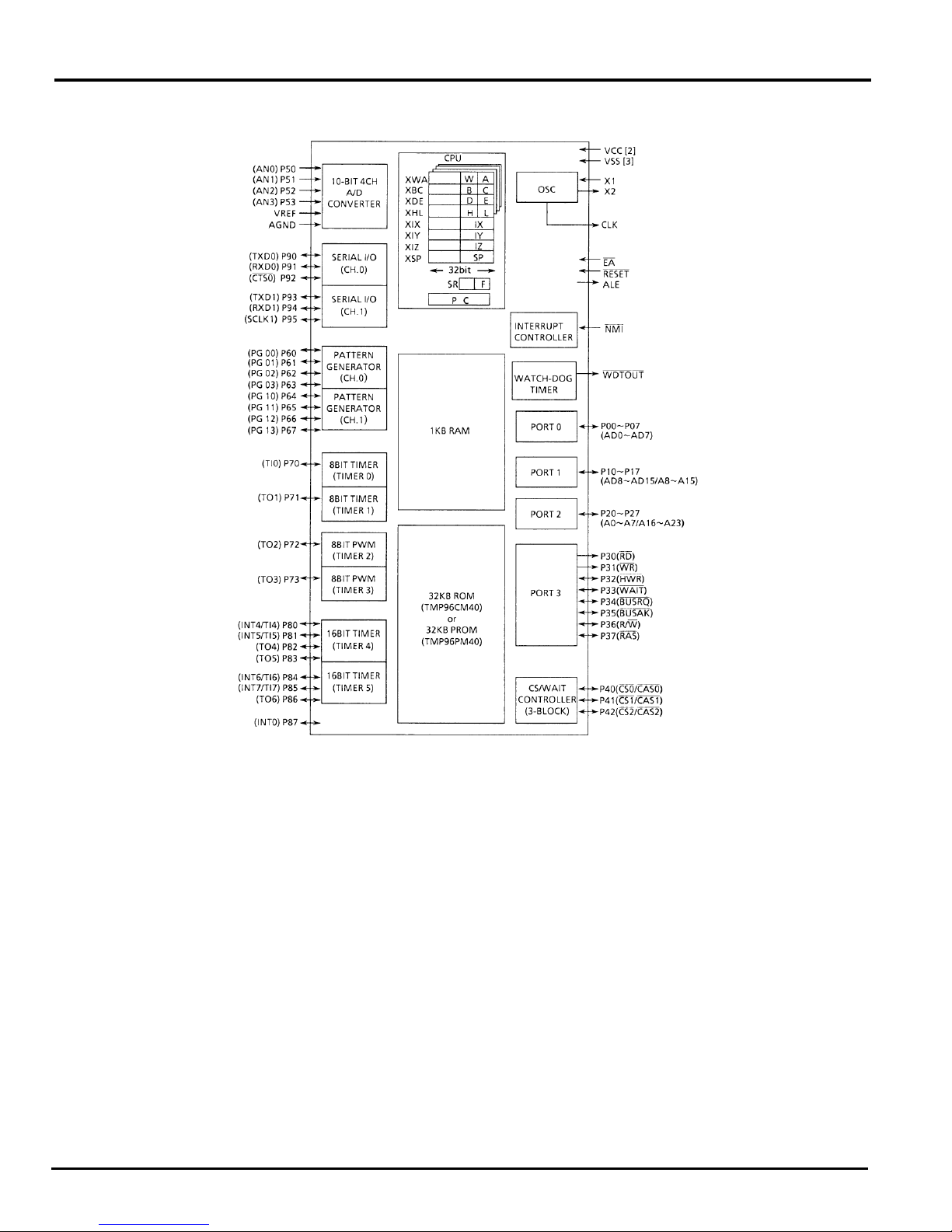
TMP96C141AF
2
Figure 1. TMP96C141AF Block Diagram
TOSHIBA CORPORATION
Page 3
TMP96C141AF
2. Pin Assignment and Functions
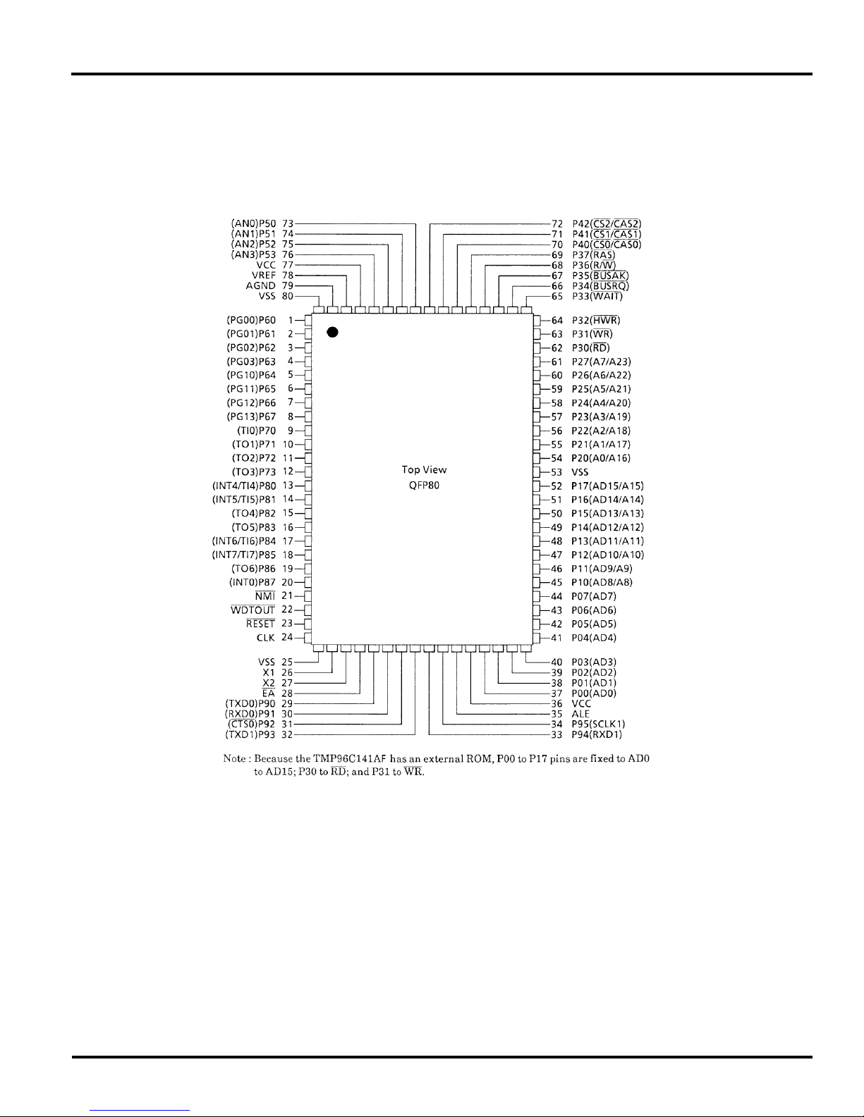
The assignment of input/output pins for TMP96C141AF, their
name and outline functions are described below.
2.1 Pin Assignment
Figure 2.1 shows pin assignment of TMP96C141AF.
TOSHIBA CORPORATION
Figure 2.1 Pin Assignment (80-pin QFP)
3
Page 4
TMP96C141AF
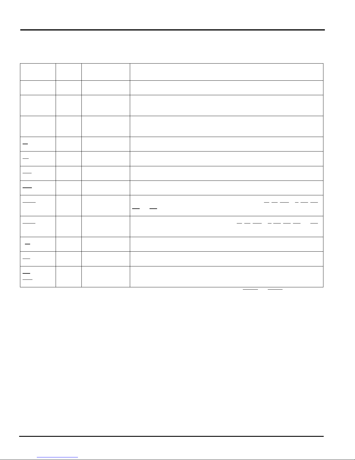
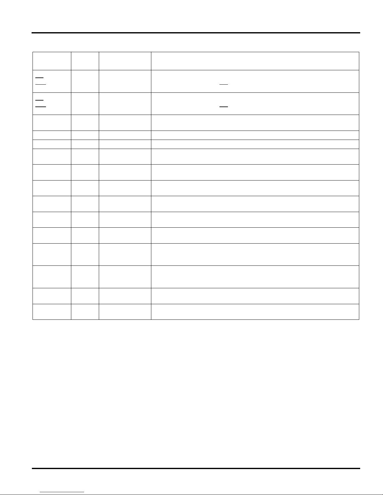
2.2 Pin Names and Functions
The names of input/output pins and their functions are described below.
Table 2.2. Pin Names and Functions
Pin Name
P00 ~ P07
AD0 ~ AD7
P10 ~ P17
AD8 ~ AD15
A8 ~ A15
P20 ~ P27
A0 ~ A7
A16 ~ A23
P30
RD
P31
WR
P32
HWR
P33
WAIT
P34
BUSRQ 1
P35
BUSAK
P36
R/W
P37
RAS
P40
CS0
CAS0
Note: With the external DMA controller, this device’s built-in memory or built-in I/O cannot be accessed using the BUSRQ
Number
of Pins
8
8
8
1
1
1
1
1
1
1
1
I/O Functions
I/O
Tri-state
I/O
Tri-state
Output
I/O
Output
Output
Output
Output
Output
Output
I/O
Output
I/O
Input
I/O
Input
I/O
Output
I/O
Output
I/O
Output
I/O
Output
Output
Port 0: I/O port that allows I/O to be selected on a bit basis
Address / data (lower): 0 - 7 for address / data bus
Port 1: I/O port that allows I/O to be selected on a bit basis
Address data (upper): 8 - 15 for address / data bus
Address: 8 to 15 for address bus
Port 2: I/O port that allows selection of I/O on a bit basis (with pull-down resistor)
Address: 0 - 7 for address bus
Address: 16 - 23 for address bus
Port 30: Output port
Read: Strobe signal for reading external memory
Port 31: Output port
Write: Strobe signal for writing data on pins AD0 -7
Port 32: I/O port (with pull-up resistor)
High write: Strobe signal for writing data on pins AD8 - 15
Port 33: I/O port (with pull-up resistor)
Wait: Pin used to request CPU bus wait
Port 34: I/O port (with pull-up resistor)
Bus request: Signal used to request high impedance for AD0 - 15, A0 - 23, RD, WR, HWR, R/W, RAS, CS0,
CS1
, and CS2 pins. (For external DMAC)
Port 35: I/O (with pull-up resistor)
Bus acknowledge: Signal indicating that AD0 - 15, A0 - 23, RD, WR, HWR, R/W, RAS, CS0, CS1, and CS2
pins are at high impedance after receiving BUSRQ. (For external DMAC)
Port 36: I/O port (with pull-up resistor)
Read/write: 1 represents read or dummy cycle; 0, write cycle.
Port 37: I/O port (with pull-up resistor)
Row address strobe: Outputs RAS strobe for DRAM.
Port 40: I/O port (with pull-up resistor)
Chip select 0: Outputs 0 when address is within specified address area.
Column address strobe 0: Outputs CAS strobe for DRAM when address is within specified address area.
and BUSAK pins.
4
TOSHIBA CORPORATION
Page 5
TMP96C141AF
Pin Name
P41
CS1
CAS1
P42
CS2
CAS2
P50 ~ P53
AN0 ~ AN3
Number
of Pins
1
1
4
I/O Functions
I/O
Output
Output
I/O
Output
Output
Input
Input
Port 41: I/O port (with pull-up resistor)
Chip select 1: Outputs 0 if address is within specified address area.
Column address strobe 1: Outputs CAS
strobe for DRAM if address is within specified address area.
Port 42: I/O port (with pull-up resistor)
Chip select 2: Outputs 0 if address is within specified address area.
Column address strobe 2: Outputs CAS
strobe for DRAM if address is within specified address area.
Port 5: Input port
Analog input: Input to A/D converter
VREF 1 Input Pin for reference voltage input to A/D converter
AGND 1 Input Ground pin for A/D converter
P60 ~ P63
PG00 ~ PG03
P64 ~ P67
PG10 ~ PG13
P70
T10
P71
T01
P72
T02
P73
T03
P80
TI4
INT4
P81
TI5
INT5
P82
TO4
P83
TO5
4
4
1
1
1
1
1
1
1
1
I/O
Output
I/O
Output
I/O
Input
I/O
Output
I/O
Output
I/O
Output
I/O
Input
Input
I/O
Input
Input
I/O
Output
I/O
Output
Ports 60 - 63: I/O ports that allow selection of I/O on a bit basis (with pull-up resistor)
Pattern generator ports: 00 - 03
Ports 64 - 67: I/O ports that allow selection of I/O on a bit basis (with pull-up resistor)
Pattern generator ports: 10 - 13
Port 70: I/O port (with pull-up resistor)
Timer input 0: Timer 0 input
Port 71: I/O port (with pull-up resistor)
Timer output 1: Timer 0 or 1 output
Port 72: I/O port (with pull-up resistor)
PWM output 2: 8-bit PWM timer 2 output
Port 73: I/O port (with pull-up resistor)
PWM output 3: 8-bit PWM timer 3 output
Port 80: I/O port (with pull-up resistor)
Timer input 4: Timer 4 count/capture trigger signal input
Interrupt request pin 4: Interrupt request pin with programmable rising/falling edge
Port 81: I/O port (with pull-up resistor)
Timer input 5: Timer 4 count/capture trigger signal input
Interrupt request pin 5: Interrupt request pin with rising edge
Port 82: I/O port (with pull-up resistor)
Timer output 4: Timer 4 output pin
Port 83: I/O port (with pull-up resistor)
Timer output 5: Timer 4 output pin
TOSHIBA CORPORATION
5
Page 6
TMP96C141AF
Pin Name
P84
TI6
INT6
P85
TI7
INT7
P86
TO6
P87
INT0
P90
TXD0
P91
RXD0
P92
CTS0
P93
TXD1
P94
RXD1
P95
SCLK1
WDTOUT
NMI
Number
of Pins
1
1
1
1
1
1
1
1
1
1
I/O Functions
I/O
Input
Input
I/O
Input
Input
I/O
Output
I/O
Input
I/O
Output
I/O
Input
I/O
Input
I/O
Output
I/O
Input
I/O
I/O
Port 84: I/O port (with pull-up resistor)
Timer input 6: Timer 5 count/capture trigger signal input
Interrupt request pin 6: Interrupt request pin with programmable rising/falling edge
Port 85: I/O port (with pull-up resistor)
Timer input 7: Timer 5 count/capture trigger signal input
Interrupt request pin 7: Interrupt request pin with rising edge
Port 86: I/O port (with pull-up resistor)
Timer output 6: Timer 5 output pin
Port 87: I/O port (with pull-up resistor)
Interrupt request pin 0: Interrupt request pin with programmable level/rising edge
Port 90: I/O port (with pull-up resistor)
Serial send data 0
Port 91: I/O port (with pull-up resistor)
Serial receive data 0
Port 92: I/O port (with pull-up resistor)
Serial data send enable 0 (Clear to Send)
Port 93: I/O port (with pull-up resistor)
Serial send data 1
Port 94: I/O port (with pull-up resistor)
Serial receive data 1
Port 95: I/O port (with pull-up resistor)
Serial clock I/O 1
1 Output Watchdog timer output pin
1 Input
Non-maskable interrupt request pin: Interrupt request pin with falling edge.
Can also be operated at rising edge by program.
CLK 1 Output Clock output: Outputs X1 ÷ 4 clock. Pulled-up during reset.
EA
1 Input
External access: 0 should be inputted with TMP96C141AF
1, with TMP96CM40F/TMP96PM40F.
ALE 1 Output Address latch enable
RESET
1 Input Reset: Initializes LSI. (With pull-up resistor)
X1/X2 2 I/O Oscillator connecting pin
VCC 2 Power supply pin (+ 5V)
VSS 3 GND pin (0V)
Note: Pull-up/pull-down resistor can be released from the pin by software.
6
TOSHIBA CORPORATION
Page 7

TMP96C141AF
3. Operation
This section describes in blocks the functions and basic operations of the TMP96C141AF device.
Check the chapter Guidelines and Restrictions for proper
care of the device.
3.1 CPU
The TMP96C141AF device has a built-in high-performance
16-bit CPU. (For CPU operation, see TLCS-900 CPU in the
book Core Manual Architecture User Manual.)
This section describes CPU functions unique to
TMP96C141AF that are not described in that manual.
3.1.1 Reset
To reset the TMP96C141AF, the RESET
0 for at least 10 system clocks (10 states: 1 µ s with a 20MHz
system clock) within an operating voltage range and with a
stable oscillation.
When reset is accepted, the CPU sets as follows:
• Program counter (PC) to 8000H.
input must be kept at
• Stack pointer (XSP) for system mode to 100H.
• SYSM bit of status register (SR) to 1. (Sets to system mode.)
• IFF2 to 0 bits of status register to 111. (Sets mask register to
interrupt level 7.)
• MAX bit of status register to 0. (Sets to minimum mode.)
• Bits RFP2 to 0 of status register to 000. (Sets register banks
to 0.)
When reset is released, instruction execution starts from
address 8000H. CPU internal registers other than the above
are not changed.
When reset is accepted, processing for built-in I/Os,
ports, and other pins is as follows:
• Initializes built-in I/O registers as per specifications.
• Sets port pins (including pins also used as built-in I/Os) to
general-purpose input/output port mode (sets I/O ports to
input ports).
• Sets the WDTOUT pin to 0. (Watchdog timer is set to enable
after reset.)
• Pulls up the CLK pin to 1.
• Sets the ALE pin to 0.
TOSHIBA CORPORATION
7
Page 8
TMP96C141AF
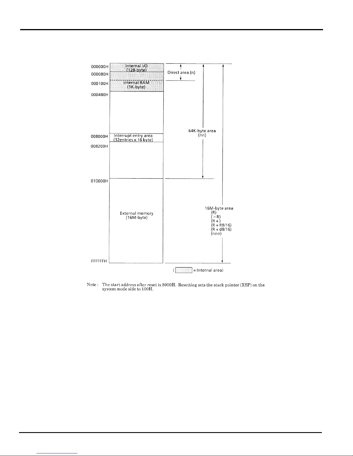
3.2 Memory Map
Figure 3.2 is a memory map of the TMP96C141AF.
8
Figure 3.2 Memory Map
TOSHIBA CORPORATION
Page 9

TMP96C141AF
3.3 Interrupts
The TLCS-900 interrupts are controlled by the CPU interrupt
mask flip-flop (IFF2 to 0) and the built-in interrupt controller.
The TMP96C141AF have altogether the following 23
interrupt sources:
• Interrupts from the CPU
…
3
(Software interrupts, privileged violations, and Illegal (undefined) instruction execution)
• Interrupts from external pins (NMI, INT0, and INT4 to 7)
• Interrupts from built-in I/Os
…
14
sends the value of the priority of the interrupt source to the
CPU. When more than one interrupt is generated simultaneously, the interrupt controller sends the value of the highest
priority (7 for non-maskable interrupts is the highest) to the
CPU.
The CPU compares the value of the priority sent with the
value in the CPU interrupt mask register (IFF2 to 0). If the value
is greater than that of the CPU interrupt mask register, the
interrupt is accepted. The value in the CPU interrupt mask register (IFF2 to 0) can be changed using the EI instruction (contents of the EI num/IFF<2:0> = num). For example,
programming EI 3 enables acceptance of maskable interrupts
with a priority of 3 or greater, and non-maskable interrupts
which are set in the interrupt controller. The DI instruction
A fixed individual interrupt vector number is assigned to
each interrupt source; six levels of priority (variable) can also
be assigned to each maskable interrupt. Non-maskable interrupts have a fixed priority of 7.
When an interrupt is generated, the interrupt controller
…
6
(IFF<2:0> = 7) operates in the same way as the EI 7 instruction. Since the priority values for maskable interrupts are 0 to 6,
the DI instruction is used to disable maskable interrupts to be
accepted. The EI instruction becomes effective immediately
after execution. (With the TLCS-90, the EI instruction becomes
effective after execution of the subsequent instruction.)
In addition to the general-purpose interrupt processing
mode described above, there is also a high-speed micro DMA
processing mode. High-speed micro DMA is a mode used by
the CPU to automatically transfer byte or word data. It enables
the CPU to process interrupts such as data saves to built-in I/Os
at high speed.
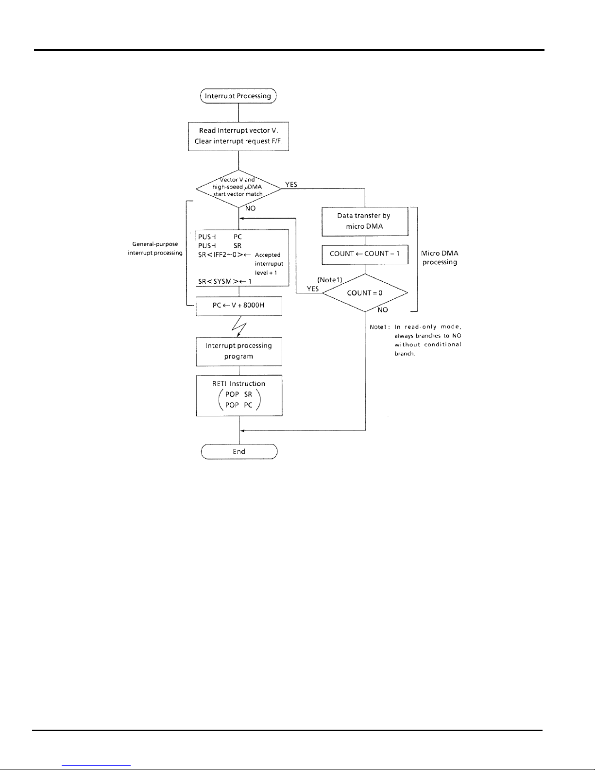
Figure 3.3 (1) is a flowchart showing overall interrupt
processing.
TOSHIBA CORPORATION
9
Page 10
TMP96C141AF
Figure 3.3 (1) Interrupt Processing Flowchart
10
TOSHIBA CORPORATION
Page 11
3.3.1 General-Purpose Interrupt Processing
When accepting an interrupt, the CPU operates as follows:
(1) The CPU reads the interrupt vector from the interrupt
controller. When more than one interrupt with the same
level is generated simultaneously, the interrupt controller
generates interrupt vectors in accordance with the
default priority (which is fixed as follows: the smaller the
vector value, the higher the priority), then clears the interrupt request.
(2) The CPU pushes the program counter and the status
register to the system stack area (area indicated by the
system mode stack pointer).
(3) The CPU sets a value in the CPU interrupt mask register
<IFF2 to 0> that is higher by 1 than the value of the
accepted interrupt level. However, if the value is 7, 7 is
set without an increment.
(4) The CPU sets the <SYSM> flag of the status register to 1
and enters the system mode.
(5) The CPU jumps to address 8000H + interrupt vector,
then starts the interrupt processing routine.
TMP96C141AF
Bus Width of Stack
Area
8 bit 23 19
16 bit 17 15
To return to the main routine after completion of the interrupt processing, the RETI instruction is usually used. Executing
this instruction restores the contents of the program counter
and the status registers.
Though acceptance of non-maskable interrupts cannot
be disabled by program, acceptance of maskable interrupts
can. A priority can be set for each source of maskable interrupts. The CPU accepts an interrupt request with a priority
higher than the value in the CPU mask register <IFF2 to 0>.
The CPU mask register <IFF2 to 0> is set to a value higher by
1 than the priority of the accepted interrupt. Thus, if an interrupt with a level higher than the interrupt being processed is
generated, the CPU accepts the interrupt with the higher level,
causing interrupt processing to nest. The CPU does not
accept an interrupt request of the same level as that of the
interrupt being processed.
Resetting initializes the CPU mask registers <IFF2 to 0>
to 7; therefore, maskable interrupts are disabled.
The addresses 008000H to 0081FFH (512 bytes) of the
TLCS-900 are assigned for interrupt processing entry area.
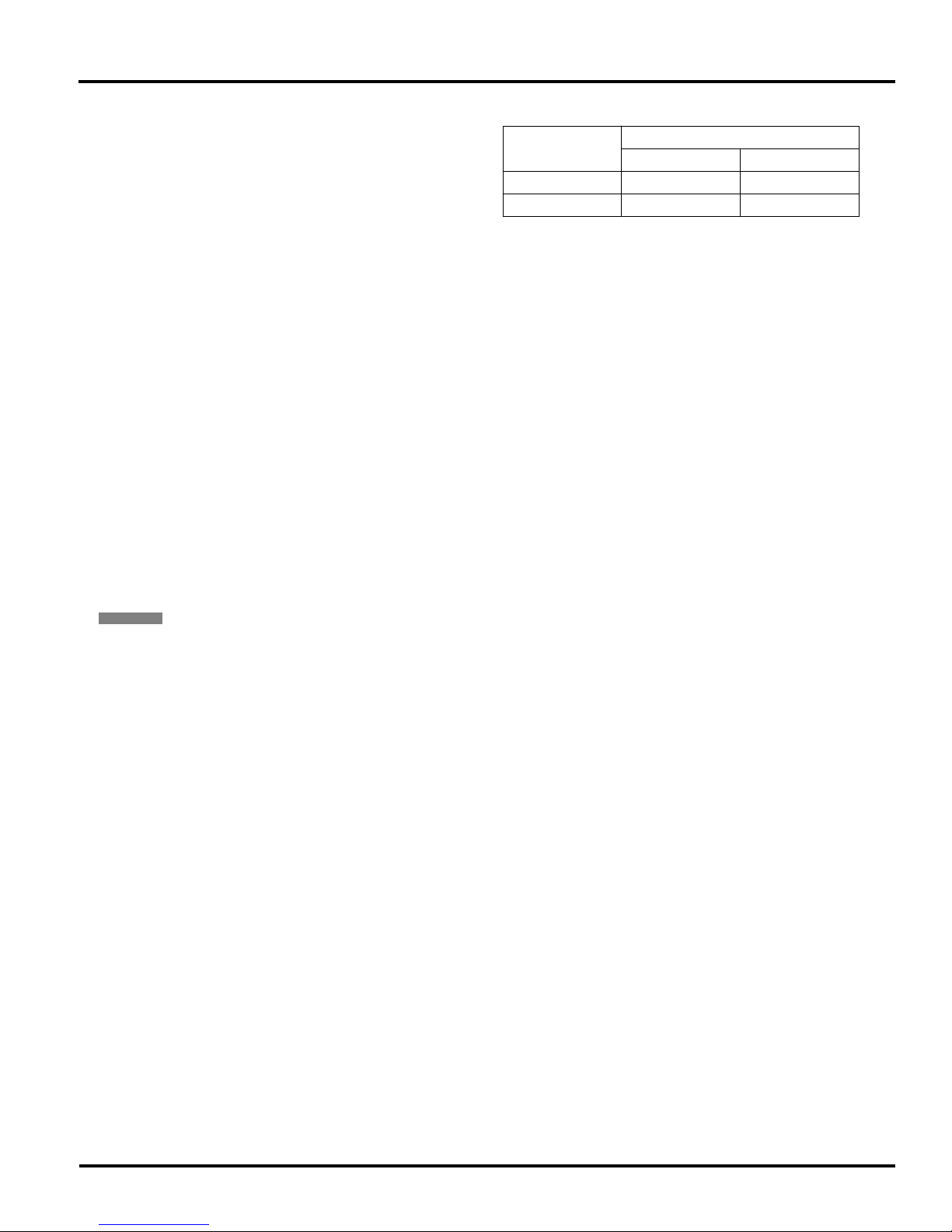
Interrupt Processing State Number
MAX mode Min mode
In minimum mode, all the above processing is completed
15 states
in (1.5
µ
s @ 20MHz). In maximum mode, it is com-
pleted in 17 states.
TOSHIBA CORPORATION
11
Page 12
TMP96C141AF
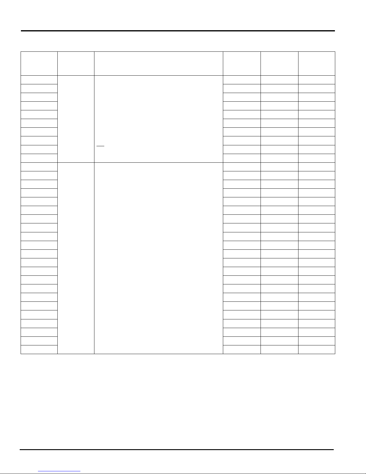
Table 3.3 (1) TMP96C141AF Interrupt Table
Default Priority Type Interrupt Source
1
2 INTPREV: Privileged violation, or SWI1 0010H 8010H –
3 INTUNDEF: Illegal instruction, or SWI2 0020H 8020H –
4 SWI 3 Instruction 0030H 8030H –
5 SWI 4 Instruction 0040H 8040H –
6 SWI 5 Instruction 0050H 8050H –
7 SWI 6 Instruction 0060H 8060H –
8 SWI 7 Instruction 0070H 8070H –
9 NMI
10 INTWD: Watchdog timer 0090H 8090H 09H
11
12 INT4 pin 00B0H 80B0H 0BH
13 INT5 pin 00C0H 80C0H 0CH
14 INT6 pin 00D0H 80D0H 0DH
15 INT7 pin 00E0H 80E0H 0EH
- (Reserved) 00F0H 80F0H 0FH
16 INTT0: 8-bit timer 0 0100H 8100H 10H
17 INTT1: 8-bit timer 1 0110H 8110H 11H
18 INTT2: 8-bit timer 2/PWM0 0120H 8120H 12H
19 INTT3: 8-bit timer 3/PWM1 0130H 8130H 13H
20 INTTR4: 16-bit timer 4 (TREG4) 0140H 8140H 14H
21 INTTR5: 16-bit timer 4 (TREG5) 0150H 8150H 15H
22 INTTR6: 16-bit timer 5 (TREG6) 0160H 8160H 16H
23 INTTR7: 16-bit timer 5 (TREG7) 0170H 8170H 17H
24 INTRX0: Serial receive (Channel.0) 0180H 8180H 18H
25 INTTX0: Serial send (Channel.0) 0190H 8190H 19H
26 INTRX1: Serial receive (Channel.1) 01A0H 81A0H 1AH
27 INTTX1: Serial send (Channel.1) 01B0H 81B0H 1BH
28 INTAD: A / D conversion completion 0 1 C 0 H 81C0H 1CH
– (Reserved) 01D0H 81D0H 1DH
– (Reserved) 01E0H 81E0H 1EH
– (Reserved) 01F0H 81F0H 1FH
Non-
Maskable
Maskable
Reset , or SW10 instruction 0000H 8000H –
Pin 0080H 8080H 08H
INTO pin 00A0H 80A0H 0AH
Vector Value
“V”
Start Address
High-Speed
Micro DMA
Start Vector
3.3.2 High-Speed Micro DMA
In addition to the conventional interrupt processing, the TLCS900 also has a high-speed micro DMA function. When an
interrupt is accepted, in addition to an interrupt vector, the CPU
receives data indicating whether processing is high-speed micro
DMA mode or general-purpose interrupt. If high-speed micro
DMA mode is requested, the CPU performs high-speed micro
DMA processing.
12
The TLCS-900 can process at very high speed compared with the TLCS-90 micro DMA because it has transfer
parameters in dedicated registers in the CPU. Since those
dedicated registers are assigned as CPU control registers, they
can only be accessed by the LDC (privileged) instruction.
TOSHIBA CORPORATION
Page 13

TMP96C141AF
(1) High-Speed Micro DMA Operation
High-speed micro DMA operation starts when the accepted
interrupt vector value matches the micro DMA start vector
value set in the interrupt controller. The high-speed micro DMA
has four channels so that it can be set for up to four types of
interrupt source.
When a high-speed micro DMA interrupt is accepted,
data is automatically transferred from the transfer source
address to the transfer destination address set in the control
register, and the transfer counter is decremented. If the value in
the counter after decrementing is other than 0, high-speed
micro DMA processing is completed. If the value in the counter
after decrementing is 0, general-purpose interrupt processing
is performed. In read-only mode, which is provided for DRAM
refresh, the value in the counter is ignored and dummy read is
repeated.
The 32-bit control registers are used for setting transfer
source/destination addresses. However, the TLCS-900 has
only 24 address pins for output. A 16M-byte space is available
for the high-speed micro DMA. Also in normal mode operation,
the all address space (in other words, the space for system
mode which is set by the CS/WAIT controller) can be
accessed by high-speed micro DMA processing.
There are two data transfer modes: one-byte mode and
one-word mode. Incrementing, decrementing, and fixing the
transfer source/destination address after transfer can be done
in both modes. Therefore data can easily be transferred
betweenI/O and memory and between I/Os. For details of
transfer modes, see the description of transfer mode registers.
The transfer counter has 16 bits, so up to 65536 transfers (the maximum when the initial value of the transfer counter
is 0000H) can be performed for one interrupt source by highspeed micro DMA processing.
A the data transferred by the µ DMA function, the transfer
nter was decreased.
When this counter is “0”H, the processor operates general interrupt processing. At this time if the same channel of
interrupt is required next interrupt, the transfer counter starts
from 65536.
Interrupt sources processed by high-speed micro DMA
processing are those with the high-speed micro DMA start
vectors listed in Table 3.3 (1).
TOSHIBA CORPORATION
13
Page 14
TMP96C141AF
The following timing chart is a high-speed µ DMA cycle of
the Transfer Address Increment mode (the other mode exe-
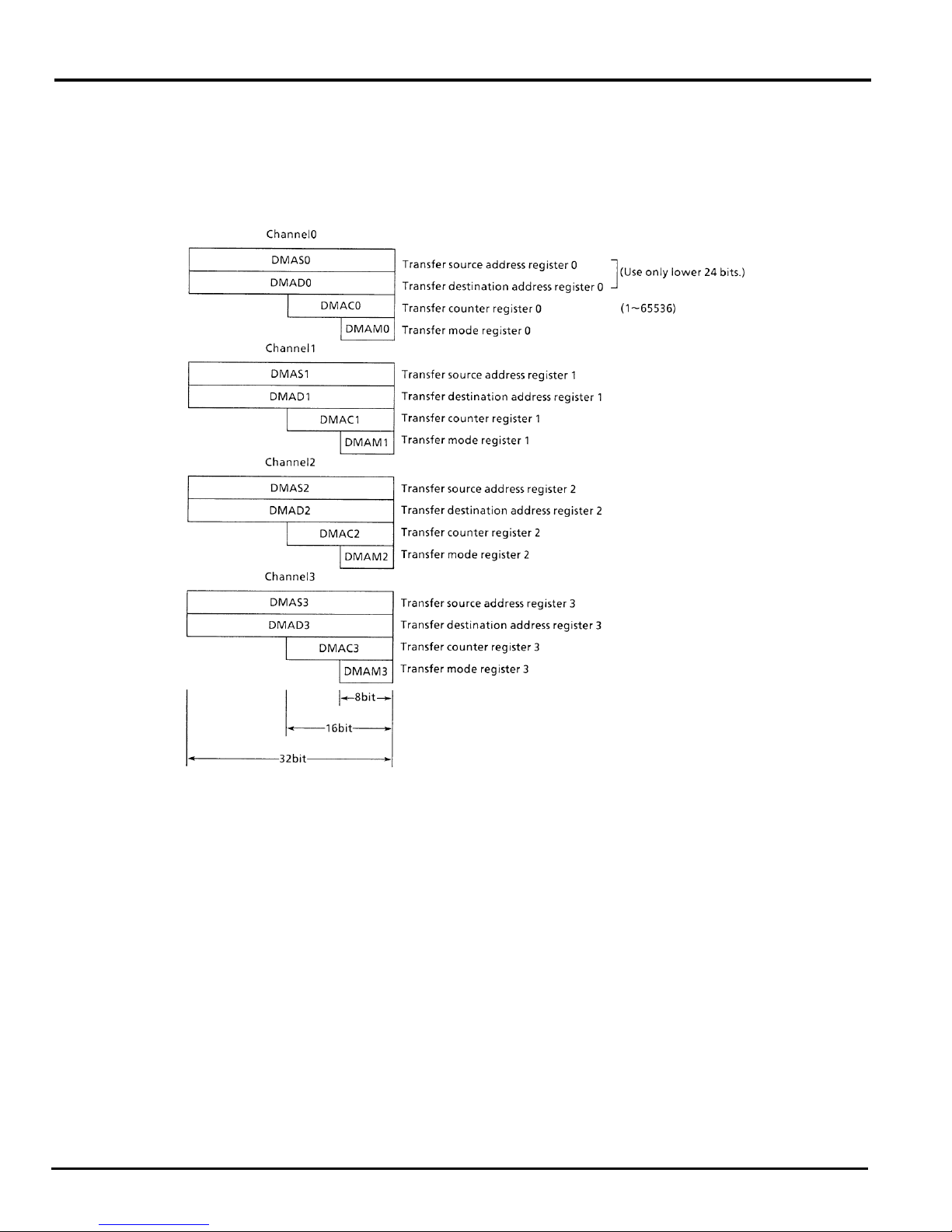
(2) Register Configuration (CPU Control Register)
cept the Read-only mode is same as this)
(Condition: MIN mode, 16bit Bus width for 16M Byte, 0 wait)
These Control Registers cannot be set only “LCD cr, r” instruction.
14
TOSHIBA CORPORATION
Page 15
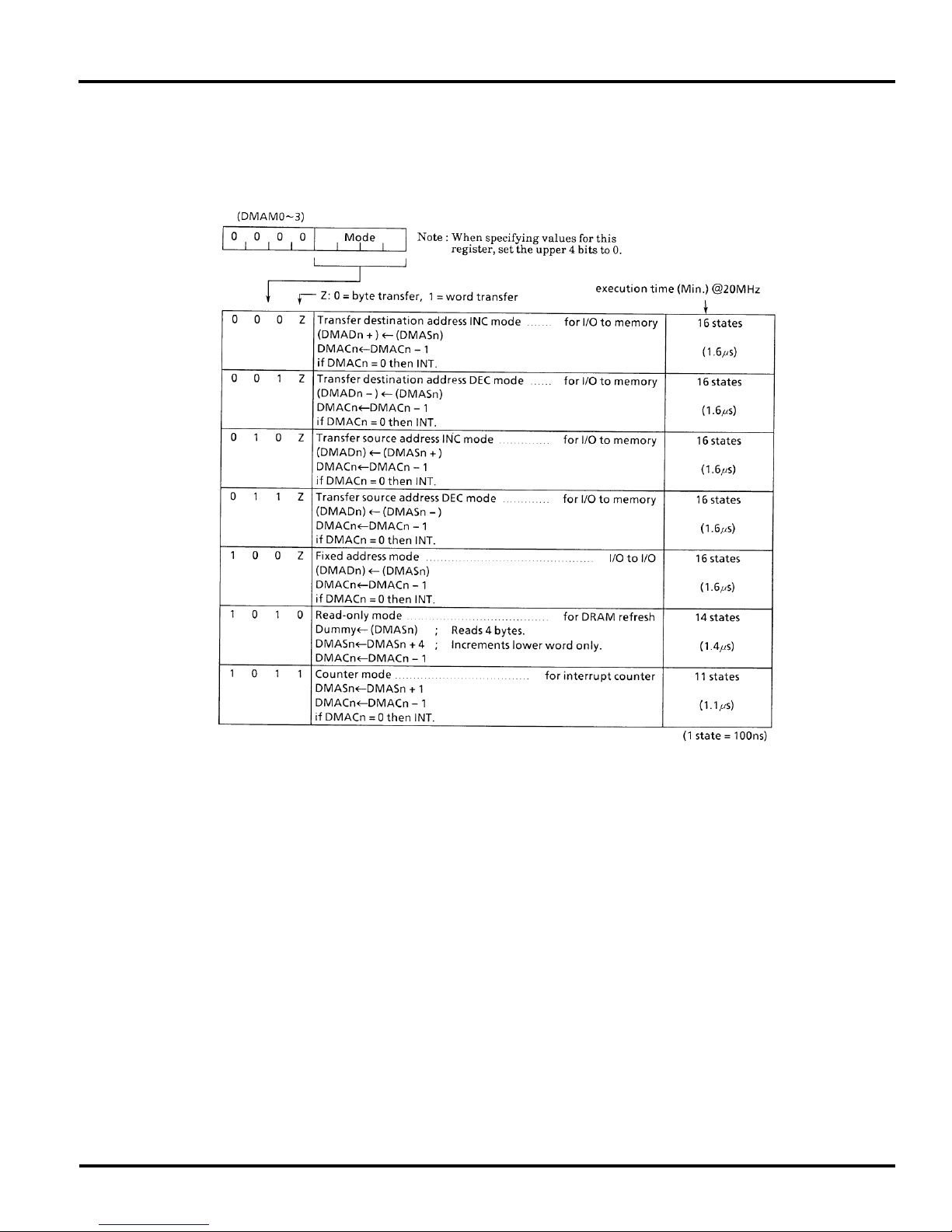
(3) Transfer Mode Register Details
TMP96C141AF
This condition is 16-bit bus width and 0 wait of source/destination address space.
Note: n: corresponds to high-speed µ DMA channels 0 - 3.
DMADn +/DMASn + : Post-increment (Increments register value after transfer.)
DMADn -/DMASn - : Post-decrement (Decrement register value after transfer.)
All address space (the space for system mode) can be
accessed by high-speed µ DMA. Do not use undefined codes
TOSHIBA CORPORATION
for transfer mode control.
15
Page 16

TMP96C141AF
➀
➁
➂
<Usage of read only mode (DRAM refresh)>
When the hardware configuration is as follows:
DRAM mapping size: = 1MB
DRAM data bus size: = 8 bits
DRAM mapping address range: = 100000H to
1FFFFFH
Set the following registers first; refresh is performed
automatically.
Register initial value setting
LD XIX, 100000H
LDC DMAS0,XIX
LD A, 00001010B
LDC DMAM0, A
…
mapping start address
…
read only mode (for
DRAM refresh)
Timer Setting
Set the timers so that interrupts are generated at
intervals of 62.5 µ s or less.
Interrupt controller setting
Set the timer interrupt mask h other interrupt mask.
Write the above timer interrupt vector value in the
High-Speed µ DMA start vector register, DMA0V.
(Operation description)
The DRAM data bus is an 8-bit bus and the micro
DMA is in read-only mode (4 bytes), so refresh is performed four times per interrupt.
When a 512 refresh/8ms DRAM is connected, DRAM
refresh is performed sufficiently if the micro DMA is
started every 15.625 µ s x 4 = 62.4 µ s or less, since the
timing is 15.625 µ s/refresh.
(Overhead)
Each processing time by the micro DMA is 1.8 µ s (18
states) @ 20MHz with an 8-bit data bus.
In the above example, the micro DMA is started every
62.5 µ s, 1.8 µ s/62.5 µ s = 0.029; thus, the overhead is
2.9%.
3.3.3 Interrupt Controller
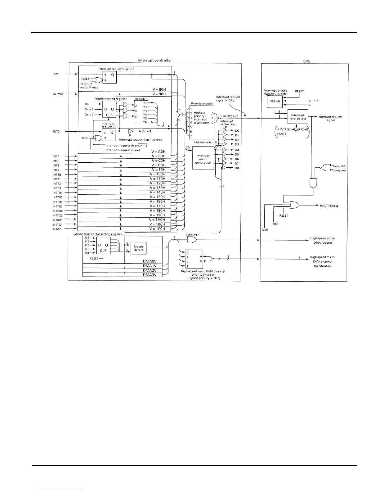
Figure 3.3.3 (1) is a block diagram of the interrupt circuits. The
left half of the diagram shows the interrupt controller; the right
half includes the CPU interrupt request signal circuit and the
HALT release signal circuit.
Each interrupt channel (total of 20 channels) in the inter-
rupt controller has an interrupt request flip-flop, interrupt prior-
ity setting register, and a register for storing the high-speed
micro DMA start vector. The interrupt request flip-flop is used
to latch interrupt requests from peripheral devices. The flip-flop
is cleared to 0 at reset, when the CPU reads the interrupt
channel vector after the acceptance of interrupt, or when the
CPU executes an instruction that clears the interrupt of that
channel (writes 0 in the clear bit of the interrupt priority setting
register).
For example, to clear the INT0 interrupt request, set the
register after the as follows.
DI instruction
INTE0AD ← ---- 0 --- Zero-clears the INT0 Flip-Flop.
The status of the interrupt request flip-flop is detected by
reading the clear bit. Detects whether there is an interrupt
request for an interrupt channel.
The interrupt priority can be set by writing the priority in
the interrupt priority setting register (e.g., INTE0AD, INTE45,
etc.) provided for each interrupt source. Interrupt levels to be
set are from 1 to 6. Writing 0 or 7 as the interrupt priority disables the corresponding interrupt request. The priority of the
non-maskable interrupt (NMI
pin, watchdog timer, etc.) is fixed
to 7. If interrupt requests with the same interrupt level are generated simultaneously, interrupts are accepted in accordance
with the default priority (the smaller the vector value, the higher
the priority).
The interrupt controller sends the interrupt request with
the highest priority among the simultaneous interrupts and its
vector address to the CPU. The CPU compares the priority
value <IFF2 to 0> set in the Status Register by the interrupt
request signal with the priority value sent; if the latter is higher,
the interrupt is accepted. Then the CPU sets a value higher
than the priority value by 1 in the CPU SR<IFF2 to 0>. Interrupt
requests where the priority value equals or is higher than the
set value are accepted simultaneously during the previous
interrupt routine. When interrupt processing is completed (after
execution of the RETI instruction), the CPU restores the priority
value saved in the stack before the interrupt was generated to
the CPU SR<IFF2 to 0>.
The interrupt controller also has four registers used to
store the high-speed micro other DMA start vector. These are I/
O registers; unlike other DMA registers (DMAS, DMAD, DMAM,
and DMAC), they can be accessed in either normal or system
mode. Writing the start vector of the interrupt source for the
micro DMA processing (see Table 3.3 (1)), enables the corresponding interrupt to be processed by micro DMA processing.
The values must be set in the micro DMA parameter registers
(e.g., DMAS and DMAD) prior to the micro DMA processing.
16
TOSHIBA CORPORATION
Page 17
TMP96C141AF
TOSHIBA CORPORATION
Figure 3.3.3 (1) Block Diagram of Interrupt Controller
17
Page 18
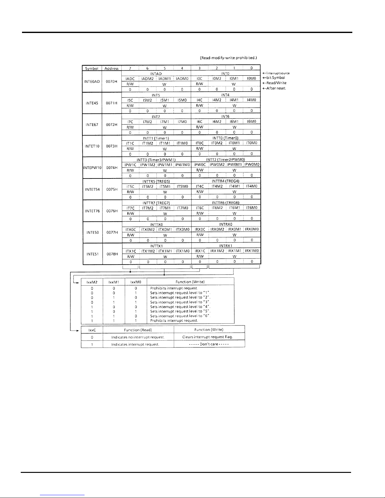
TMP96C141AF
(1) Interrupt Priority Setting Register
18
TOSHIBA CORPORATION
Page 19
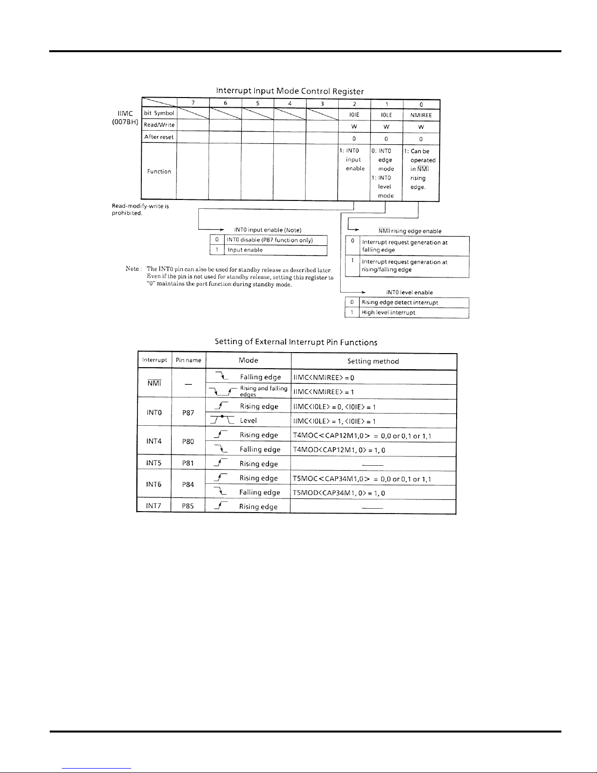
(2) External Interrupt Control
TMP96C141AF
TOSHIBA CORPORATION
19
Page 20

TMP96C141AF
(3) High-Speed Micro DMA Start Vector
When the CPU reads the interrupt vector after accepting an interrupt, it simultaneously compares the interrupt vector with each
channel’s micro DMA start vector (bits 4 to 8 of the interrupt vec-
Micro DMA0 Start Vector
76543210
DMA0V
(007CH)
bit Symbol DMA0V8 DMA0V7 DMA0V6 DMA0V5 DMA0V4
Read / Write W
After reset 00000
Micro DMA1 Start Vector
76543210
DMA1V
(007DH)
bit Symbol DMA1V8 DMA1V7 DMA1V6 DMA1V5 DMA1V4
Read / Write W
After reset 00000
Micro DMA2 Start Vector
76543210
DMA2V
(007EH)
bit Symbol DMA2V8 DMA2V7 DMA2V6 DMA2V5 DMA2V4
Read / Write W
After reset 00000
Micro DMA3 Start Vector
76543210
DMA3V
(007FH)
bit Symbol DMA3V8 DMA3V7 DMA3V6 DMA3V5 DMA3V4
Read / Write W
After reset 00000
tor). When both match, the interrupt is processed in micro
DMA mode for the channel whose value matched.
If the interrupt vector matches more than one channel, the channel with the lower channel number has a
higher priority.
(read-modify-write is not possible.)
(read-modify-write is not possible.)
(read-modify-write is not possible.)
(read-modify-write is not possible.)
(4) Notes
The instruction execution unit and the bus interface unit of this
CPU operate independently of each other. Therefore, if the instruction used to clear an interrupt request flag of an interrupt is fetched
before the interrupt is generated, it is possible that the CPU might
execute the fetched instruction to clear the interrupt request flag
20
while reading the interrupt vector after accepting the interrupt. If so, the CPU would read the default vector 00A0H
and start the interrupt processing from the address
80A0H.
To avoid this, make sure that the instruction used to
clear the interrupt request flag comes after the DI instruction.
TOSHIBA CORPORATION
Page 21
TMP96C141AF
≤
3.4 Standby Function
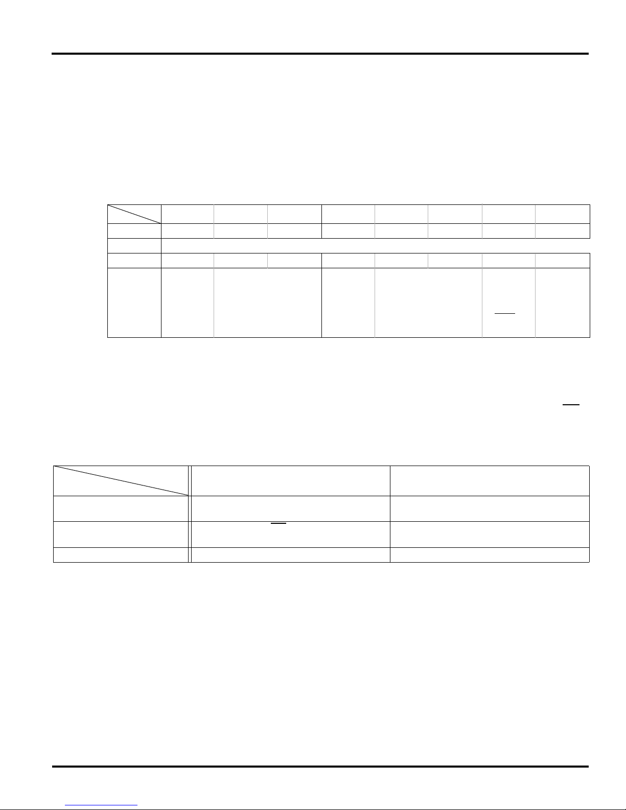
When the HALT instruction is executed, the TMP96C141AF
enters RUN, IDLE, or STOP mode depending on the contents
of the HALT mode setting register.
(1) RUN : Only the CPU halts; power consumption
remains unchanged.
(2) IDLE : Only the built-in oscillator operates, while all
76543210
WDMOD
(005CH)
Bit Symbol WDTE WDTP1 WDTP0 WARM HALTM1 HALTM0 RESCR DRVE
Read/Write R/W
After reset 10000000
1 : WDT
Enable
Function
16
00 : 2
/ fc
18
01 : 2
/ fc
20
10 : 2
/ fc
22
11 : 2
/ fc
Detection time
other built-in circuits halt. Power consumption is reduced to 1/10 or less than that during normal operation.
(3) STOP : All internal circuits including the built-in oscil-
lator halt. This greatly reduces power consumption. The states of the port pins in
STOP mode can be set as listed in Table 3.4
(1) using the I/O register
WDMOD<DRVE>bit.
Warming up
time
16
0 : 2
/fc
18
1 : 2
/fc
Standby mode
00 : RUN mode
01 : STOP mode
10 : IDLE mode
11 : Don’t care
1: Connects
watchdog
timer
output to
RESET
pin
internally.
1: Drive pin
even in
STOP
mode.
When STOP mode is released by other than a reset, the
system clock output starts after allowing some time for warming up set by the warming-up counter fro stabilizing the bulit-in
oscillator. To release STOP mode by reset, it is necessary to
Standby Release by Interrupt
Standby Mode
Interrupt Level
Can be released by any interrupt.
RUN
IDLE Can only be released by NMI
STOP ↑ (Note) ↑
After standby mode is released, interrupt processing starts.
is released, interrupt processing starts.
Interrupt Mask (IFF2 to 0)
Interrupt Request Level
or INT0 pin. After standby mode
allow the oscillator to stabilize.
To release standby mode, a reset or an interrupt is used.
To release IDLE or STOP mode, only an interrupt by the NMI or
INT0 pin, or a reset can be used. The details are described
below:
Interrupt Mask (IFF2 to 0)
> Interrupt Request Level
Can only be released by INT0 pin.
Processing resumes from address next to HALT instruction.
↑
TOSHIBA CORPORATION
21
Page 22
TMP96C141AF
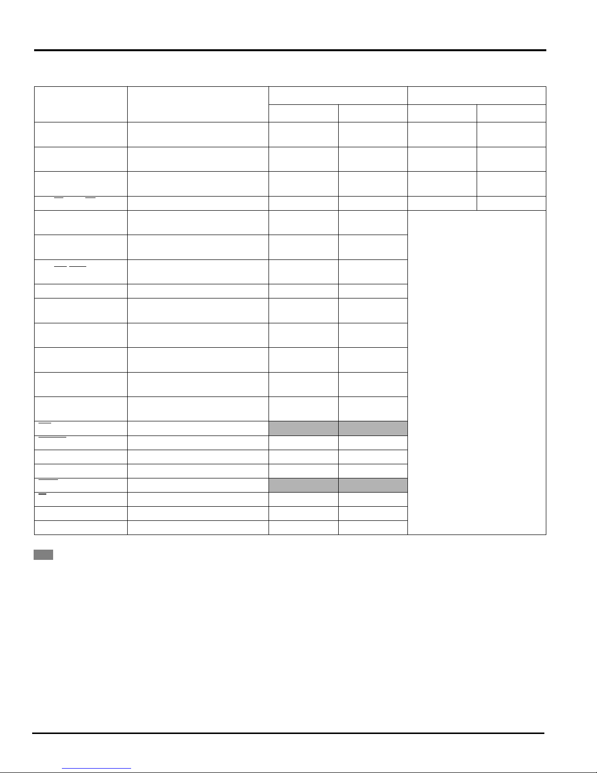
Table 3. 4 (1) Pin States in STOP Mode
Pin Name I/O
96C141AF 96CM40/96PM40
DRVE = 0 DRVE = 1 DRVE = 0 DRVE = 1
P0
P1
P2
P30 (RD
), P31 (WR) Output – “1” Output – Output
P32 ~ P37
P40, P41
P42 (CS2
/CAS2)
Input mode/AD0 ~ 7
Output mode
Input mode/AD8 ~ 15
Output mode/A8 ~ 15
Input mode
Output mode/A0 ~ 7, A16 ~ 23
Input mode
Output mode
Input mode
Output mode
Input mode
Output mode
–
x
–
x
PD*
PD*
PU
PU
PU*
PU*
PD*
PD*
–
x
–
x
PD*
Output
PU
Output
PU
Output
PD
Output
–
–
–
–
PD*
PD*
P5 Input – –
P6
P7
P80 ~ P86
P87 (INT0)
P9
NMI
WDTOUT
Input mode
Output mode
Input mode
Output mode
Input mode
Output mode
Input mode
Output mode
Input mode
Output mode
Input Input Input
Output Output Output
PU*
PU*
PU*
PU*
PU*
PU*
PU
PU
PU*
PU*
PU
Output
PU
Output
PU
Output
PU
Output
PU
Output
ALE Output “0” “0”
CLK Output – “1”
RESET
EA
Input Input Input
Input Input Input
X1 Input – –
X2 Output “1” “1”
–
Output
–
Output
PD*
Output
←
–: Input for input mode/input pin is invalid; output mode/output pin is at high impedance.
Input: Input enable state
Input: Input gate in operation. Fix input voltage to 0 or 1 so that input pin stays constant.
Output: Output state
PU: Programmable pull-up pin. Fix the pin to avoid through current since the input gate operates when a pull-up resistor is not set.
PD: Programmable pull-down pin. Fix the pin like a pull-up pin when a pull-down resistor is not set.
*: Input gate disable state. No through current even if the pin is set to high impedance.
x: Cannot set.
Note: Port registers are used for controlling programmable pull-up/pull-down. If a pin is also used for an output function (e.g., TO1) and the output function
is specified, whether pull-up or pull-down is selected depends on the output function data. If a pin is also used for an input function, whether pull-up or
pull-down is selected depends on the port register setting value only.
22 TOSHIBA CORPORATION
Page 23
TMP96C141AF
3.5 Functions of Ports
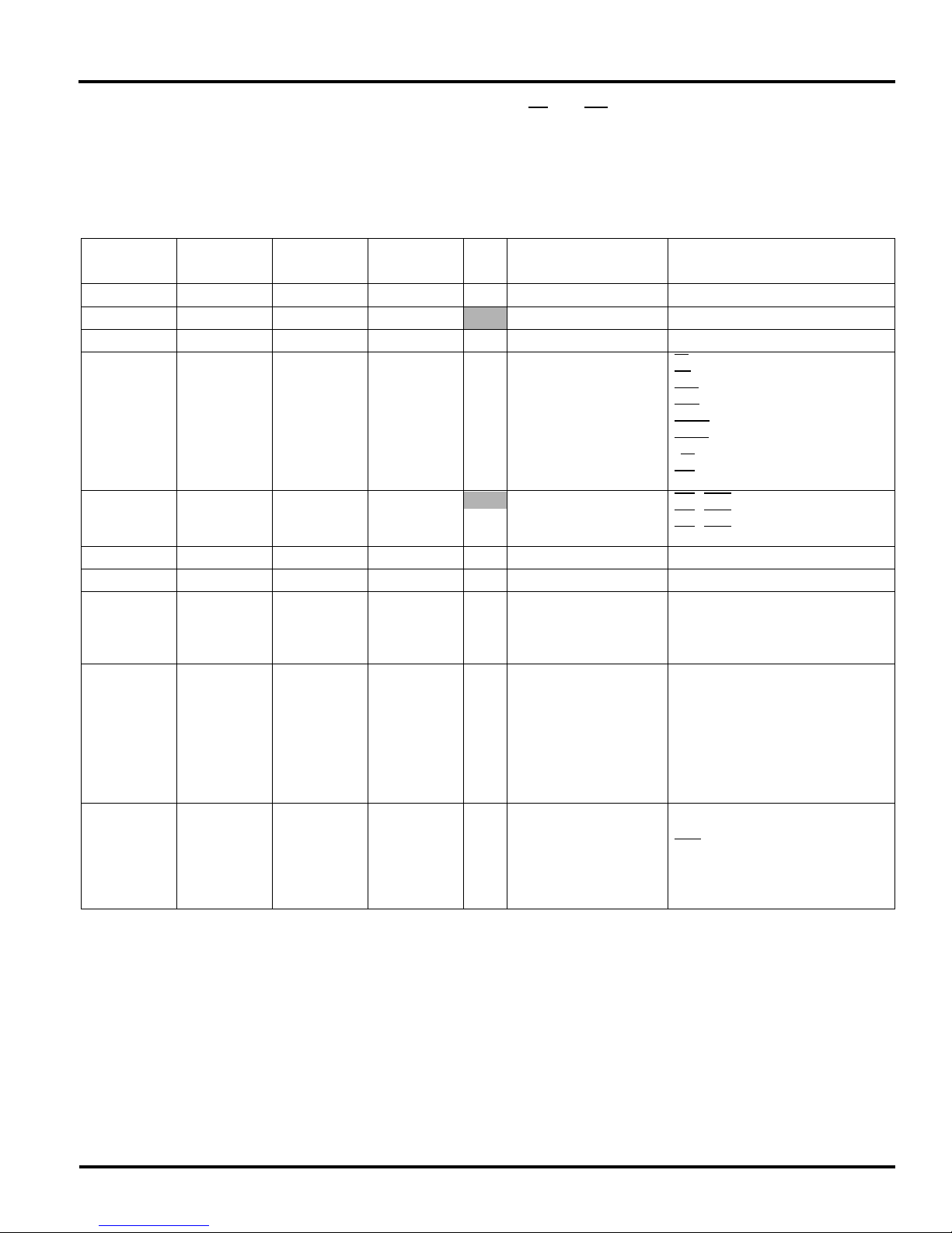
The TMP96CM40F/TMP96PM40F has 65 bits for I/O ports.
The TMP96C141AF, TMP96C041AF has 47 bits for I/O ports
because Port0, Port1, P30, and P31 are dedicated pins for
AD0 to 7, AD8 to
15, RD, and WR.
These port pins have I/O functions for the built-in CPU
and internal I/Os as well as general-purpose I/O port functions. Table 3.5 lists the function of each port pin.
(R: ↑ = With programmable pull-up resistor
↓ = WIth programmable pull-down
Table 3.5 Functions of Ports
Port Name Pin Name
Port0 P00 ~ P07 8 I/O – Bit AD0 ~ AD7
Port1 P10 ~ P17 8 I/O
Port2 P20 ~ P27 8 I/O ↓ Bit A0 ~ A7/ A16 ~ A23
Port 3 P30
P31
P32
P33
P34
P35
P36
P37
Port4 P40
P41
P42
Port5 P50 ~ P53 4 Input – (Fixed) AN0 ~ AN3
Port6 P60 ~ P67 8 I/O ↑ Bit PG00 ~ PG03, PG10 ~ PG13
Port7 P70
P71
P72
P73
Port8 P80
P81
P82
P83
P84
P85
P86
P87
Port9 P90
P91
P92
P93
P94
P95
Number of
Pins
1
1
1
1
1
1
1
1
1
1
1
1
1
1
1
1
1
1
1
1
1
1
1
1
1
1
1
1
1
Direction R Direction Setting Unit Pin Name for Built-in Function
– Bit AD8 ~ AD15/ A8 ~ A15
Output
Output
I/O
I/O
I/O
I/O
I/O
I/O
I/O
I/O
I/O
I/O
I/O
I/O
I/O
I/O
I/O
I/O
I/O
I/O
I/O
I/O
I/O
I/O
I/O
I/O
I/O
I/O
I/O
–
–
↑
↑
↑
↑
↑
↑
↑
↑
↓
↑
↑
↑
↑
↑
↑
↑
↑
↑
↑
↑
↑
↑
↑
↑
↑
↑
↑
(Fixed)
(Fixed)
Bit
Bit
Bit
Bit
Bit
Bit
Bit
Bit
Bit
Bit
Bit
Bit
Bit
Bit
Bit
Bit
Bit
Bit
Bit
Bit
Bit
Bit
Bit
Bit
Bit
Bit
Bit
RD
WR
HWR
WAIT
BUSRQ
BUSAK
R/W
RAS
CS0 / CAS0
CS1 / CAS1
CS2 / CAS2
T10
TO1
TO2
TO3
T14/INT4
T15/INT5
TO4
TO5
T16 / INT6
T17 / INT7
TO6
INT0
TXD0
RXD0
CTS0
TXD1
RXD1
SCLK1
TOSHIBA CORPORATION 23
Page 24
TMP96C141AF
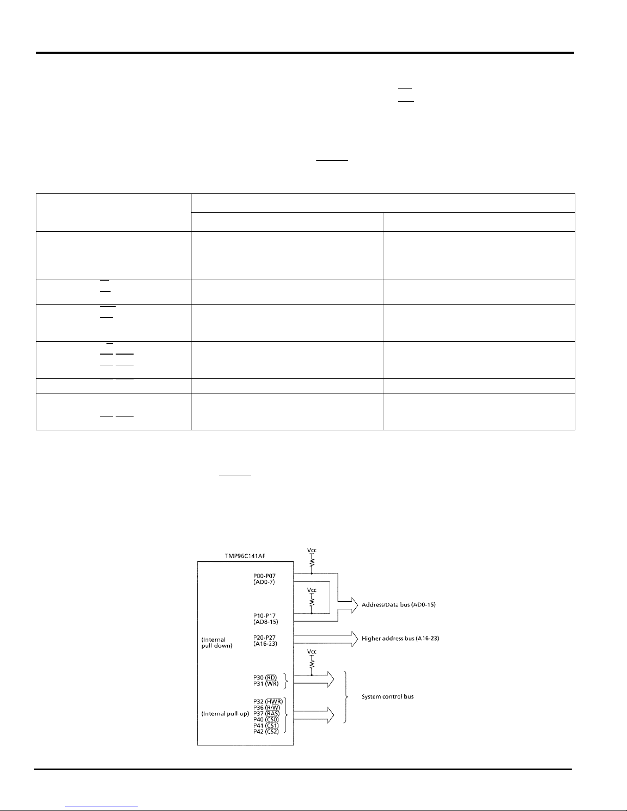
Resetting makes the port pins listed below function as
general-purpose I/O ports.
I/O pins programmable for input or output function as
input ports.
To set port pins for built-in functions, a program is
required.
Since the TMP96C141AF has an external ROM, some
ports are permanently assigned to the CPU.
Pin Name
P00 - P07
(AD0 - AD7)
P10 - P17
(AD8 - AD15)
P30 (RD
)
P31 (WR
)
P32 (HWR
P37 (RAS
P36 (R/W
P40 (CS0
P41 (CS1
P42 (CS2
P20 - P27
(A16 - A23)
P42 (CS2
)
) ↑
)
/CAS0)
/CAS1)
/CAS2) ↑ (*) ↑
/CAS2)
No status change (these pins are not “Hz”) These pins are “Hz”.
• P00 ~ P07 →AD0 ~ AD7
• P10 ~ P17 →AD8 ~ AD15
• P30 →RD
• P31 →WR
Bus release function
The TMP96C141AF has the internal pull-up and pull-
down resistors to fix the bus control signals at bus release.
Table 3.5 (1) shows the pin condition at bus release
(BUSAK) = “L”).
Pin state at bus release
Port mode Function mode
↑
↑↑
↑
These pins are “Hz”.
(“Hz” status after these pins are driven to high level.)
The output buffer is “OFF” after these pins are drinen high.
These pins are added in the internal resistor of pull-up. It’s
no relation for the value of output latch.
The output buffer is “OFF” after these pins are drinen high.
These pins are added in the internal resistor of pull-down.
It’s no relation for the value of output latch.
(*) P42 has the resistor of programmable pull-down, but
when the bus are released, P42 pin is added a resistor of pullup.
That is, when it is used for bus release (BUSAK = “0”), the
pins of below need pull-up or pull-down resistor for an external
circuit.
P00 - P07 (AD07)
P10 - P17 (AD8 - AD15)
P30 (RD)
P31 (WR)
When the bus is released, both internal memory and
internal I/O cannot be accessed. But the internal I/O continues
to run. Therefore, be careful about releasing time and set the
setection time WDT.
Figure 3.5. Example of external bus interface using bus release function.
24 TOSHIBA CORPORATION
Page 25
TMP96C141AF
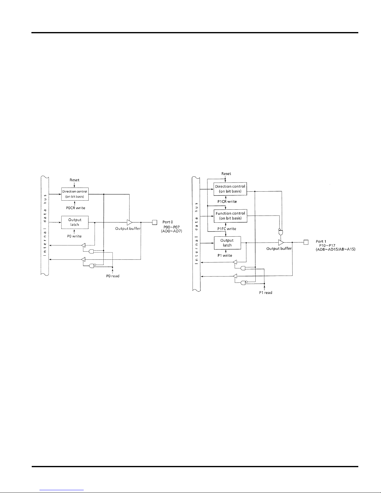
3.5.1 Port 0 (P00 - P07)
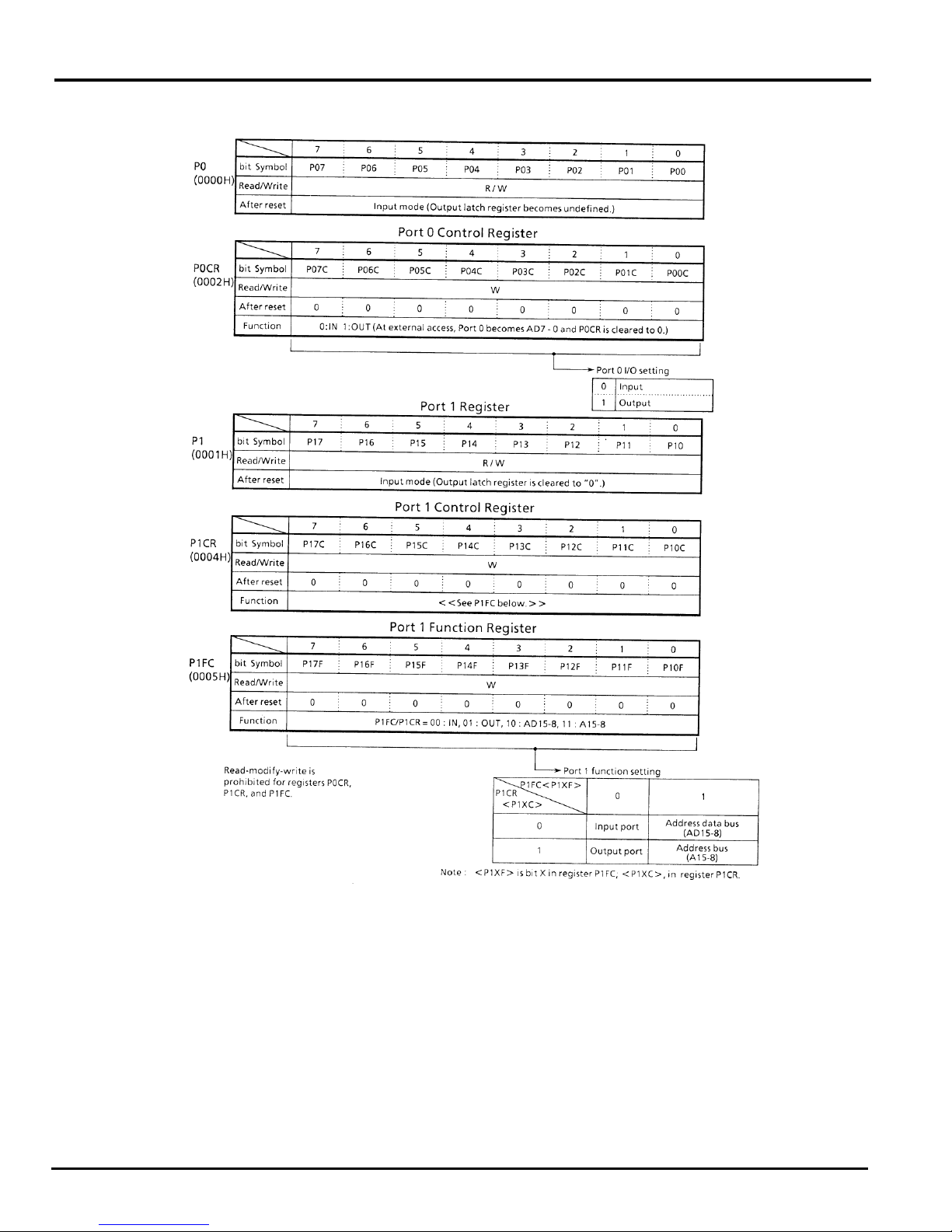
Port 0 is an 8-bit general-purpose I/O port. I/O can be set on a
bit basis using control register P0CR to 0 and sets Port 0 to
input mode.
In addition to functioning as a general purpose I/O port,
Port 0 also functions as an address data bus (AD0 to 7). To
access external memory, Port 0 functions as an address data
bus (AD 0 to 7) and all bits of the control register P0CR are
cleared to 0.
With the TMP96C141AF/TMP96C041AF, which comes
with an external ROM, Port 0 always functions as an address
data bus (AD0 to 7) regardless of the value set in control register P0CR.
3.5.2 Port 1 (P10 - P17)
Port 1 is an 8-bit general-purpose I/O port. I/O can be set on a
bit basis using control register P1CR and function register
P1FC. Resetting resets all bits of output latch P1, control register P1CR, and function register P1FC to 0 and sets Port 1 to
input mode.
In addition to functioning as a general purpose I/O port,
Port 1 also functions as an address data bus (AD8 to 15) or an
address bus (A8 to 15).
With the TMP96C141AF/TMP96C041AF, which comes
with an external ROM, Port 1 always functions as an address
data bus (AD8 to 15) regardless of the value set in control register P1CR.
Figure 3.5 (1). Port 0 Figure 3.5 (2). Port 1
TOSHIBA CORPORATION
25
Page 26
TMP96C141AF
Port 0 Register
Figure 3.5 (3). Registers for Ports 0 and 1
26
TOSHIBA CORPORATION
Page 27
TMP96C141AF
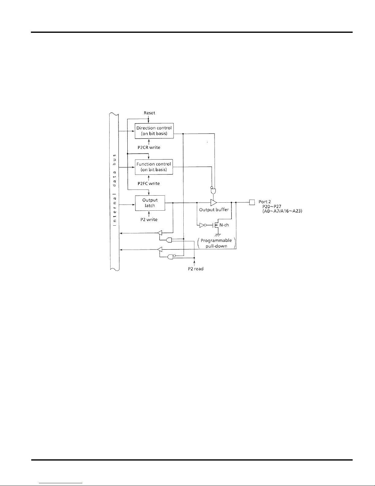
3.5.3 Port 2 (P20 - P27)
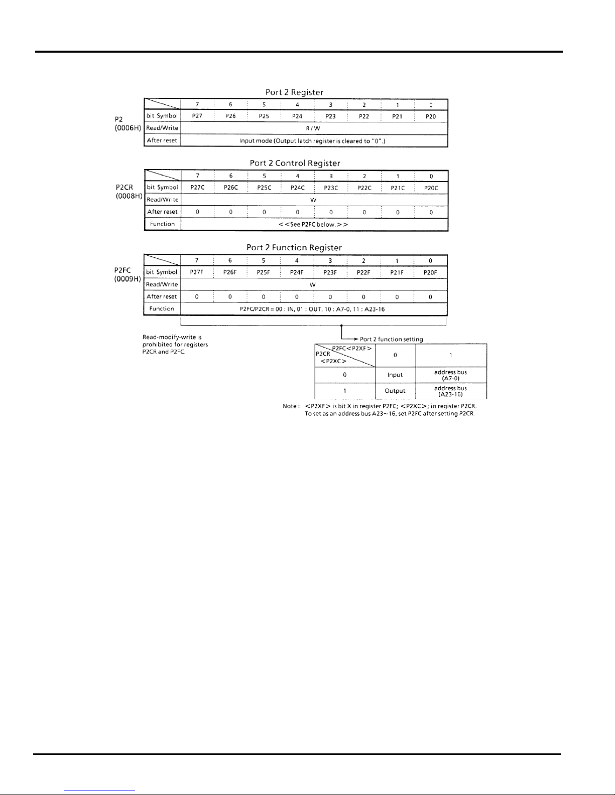
Port 2 is an 8-bit general-purpose I/O port. I/O can be set on
bit basis using the control register P2CR and function register
P2FC. Resetting resets all bits of output latch P2, control register P2CR and function register P2FC to 0. It also sets Port 2 to
input mode and connects a pull-down resistor. To disconnect
the pull-down resistor, write 1 in the output latch.
In addition to functioning as a general-purpose I/O port,
Port 2 also functions as an address data bus (A0 to 7) and an
address bus (A16 to 23).
TOSHIBA CORPORATION
Figure 3.5 (4). Port 2
27
Page 28
TMP96C141AF
28
Figure 3.5 (5). Registers for Port 2
TOSHIBA CORPORATION
Page 29

TMP96C141AF
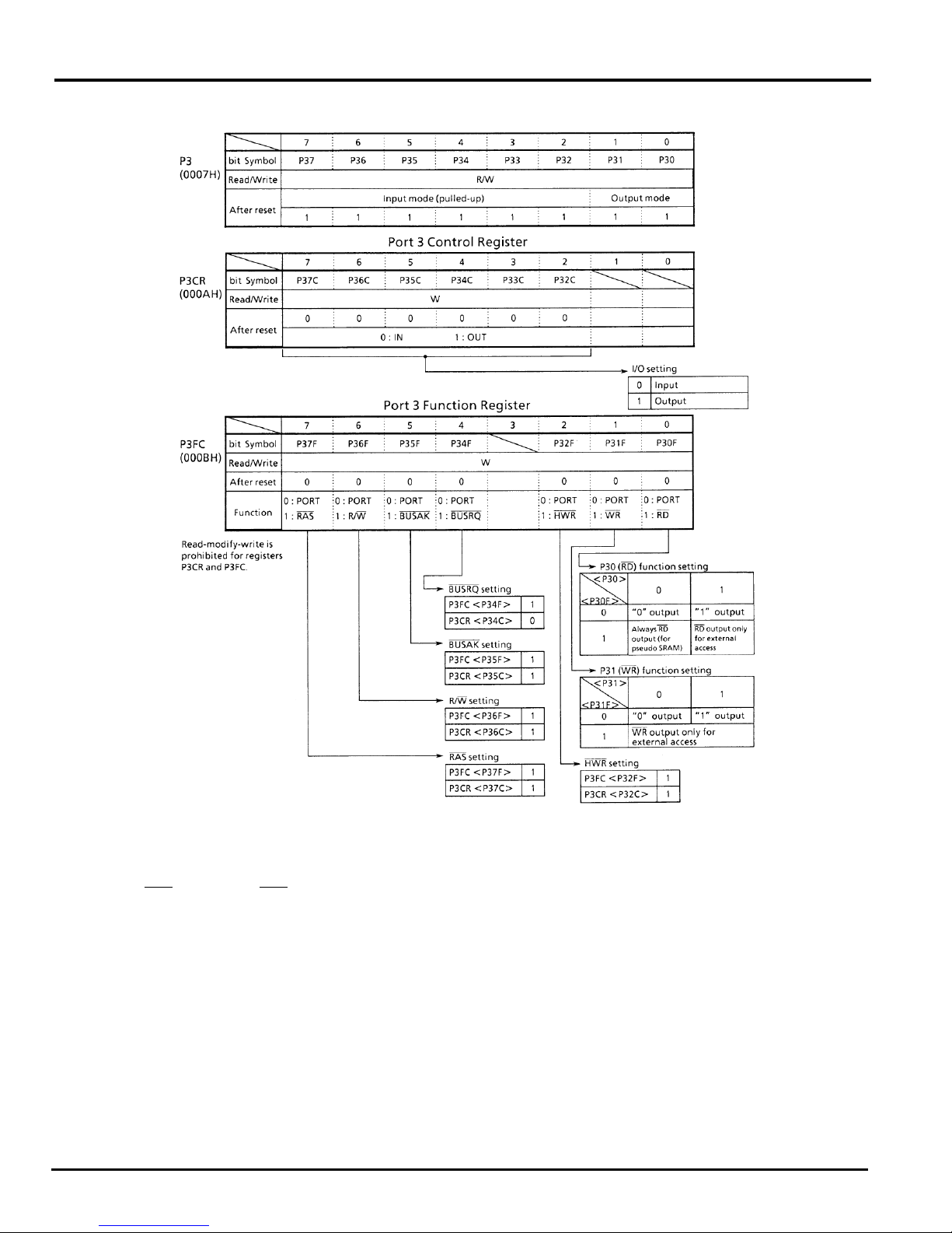
3.5.4 Port 3 (P30 - P37)
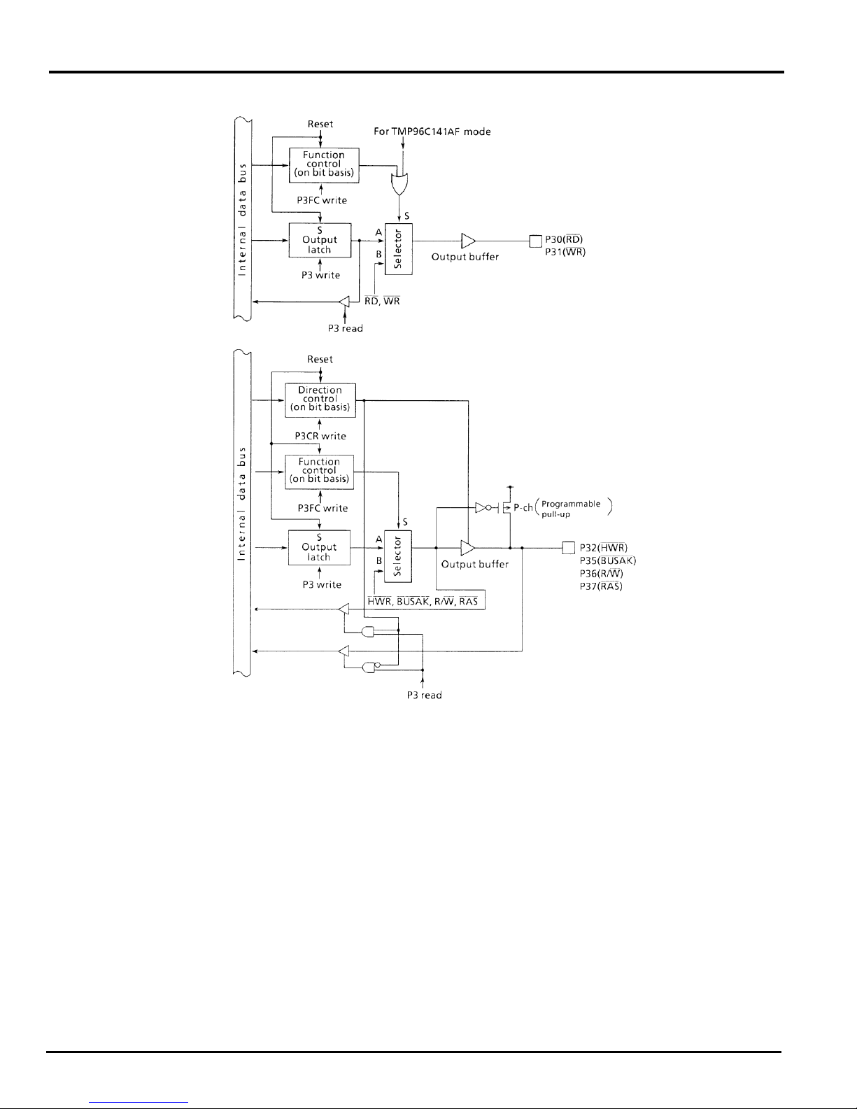
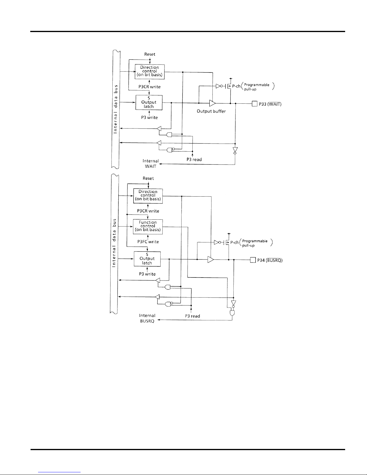
Port 3 is an 8-bit general-purpose I/O port.
I/O can be set on a bit basis, but note that P30 and P31
are used for output only. I/O is set using control register P3CR
and function register P3FC. Resetting resets all bits of output
latch P3, control register P3CR (bits 0 and 1 are unused), and
function register P3FC to 0. Resetting also outputs 1 from P30
and P31, sets P32 to P37 to input mode, and connects a pullup resistor.
In addition to functioning as a general-purpose I/O port,
Port 3 also functions as an I/O for the CPU’s control/status signal.
With the TMP96C141AF, when P30 pin is defined as RD
signal output mode (<P30F> = 1), clearing the output latch
register <P30> to 0 outputs the RD strobe (used for the
pseudo static RAM) from the P30 pin even when the internal
address area is accessed.
If the output latch register <P30> remains 1, the RD
strobe signal is output only when the external address area is
accessed.
With the TMP96C141AF/TMP96C041AF, which comes
with an external ROM, Port 30 outputs the RD signal; P31, the
WR signal, regardless of the values set in function registers
P30F and P31F.
TOSHIBA CORPORATION
29
Page 30
TMP96C141AF
Figure 3.5 (6). Port 3 (P30, P31, P32, P35, P36, P37)
30
TOSHIBA CORPORATION
Page 31
TMP96C141AF
TOSHIBA CORPORATION
Figure 3.5 (7). Port 3 (P33, P34)
31
Page 32
TMP96C141AF
Port 3 Register
Note: When P33/W
32
AIT pin is used as a WAIT pin, set P#CR <P33C> to “0” and Chip Select/Wait control register.
Figure 3.5 (8). Registers for Port 3
TOSHIBA CORPORATION
Page 33

TMP96C141AF
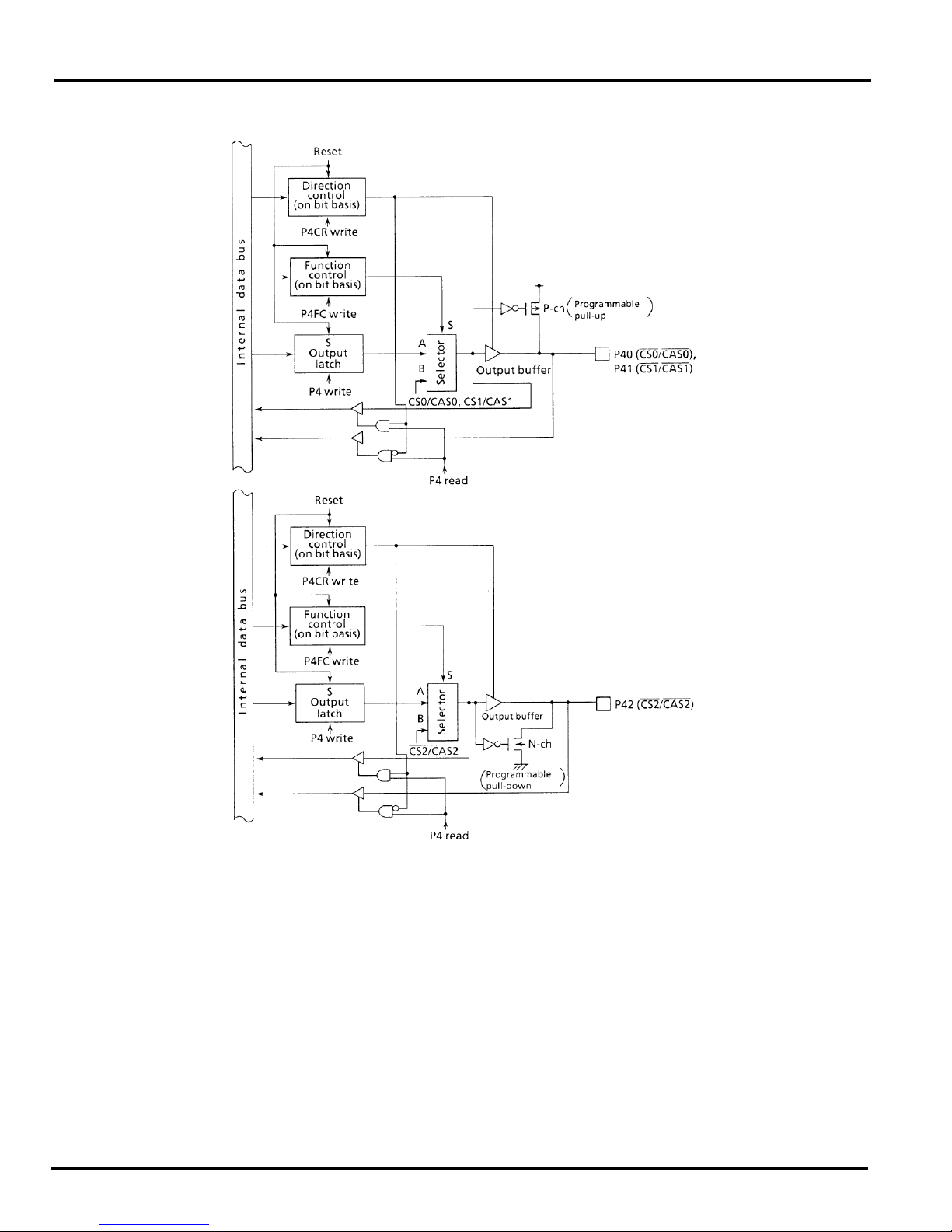
3.5.5 Port 4 (P40 - P42)
Port 4 is a 3-bit general-purpose I/O port. I/O can be set on a
bit basis using control register P4CR and function register
P4FC. Resetting does the following:
- Sets the P40 and P42 output latch registers to 1.
- Resets all bits of the P42 output latch register, the control
register P4CR, and the function register P4FC to 0.
- Sets P40 and P41 to input mode and connects a pull-up
resistor.
- Sets P42 to input mode and connects a pull-down resistor.
In addition to functioning as a general-purpose I/O port,
Port 4 also functions as a chip select output signal (CS0
CS2 or CAS0 to CAS2).
to
TOSHIBA CORPORATION
33
Page 34
TMP96C141AF
34
Figure 3.5 (9). Port 4
TOSHIBA CORPORATION
Page 35
TMP96C141AF
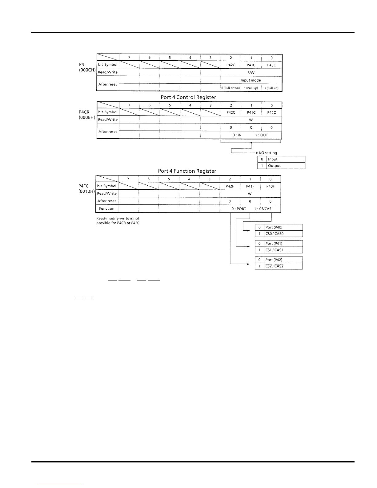
Port 4 Register
Note: To output chip select signal (CS0
bits of the control register P4CR and the function register to P4FC.
The BOCS, B1CS, and B2CS registers of the chip select/wait controller are used
to select the CS/CAS function.
/CAS0 to CS2/CAS2), set the corresponding
Figure 3.5 (10). Registers for Port 4
TOSHIBA CORPORATION
35
Page 36
TMP96C141AF
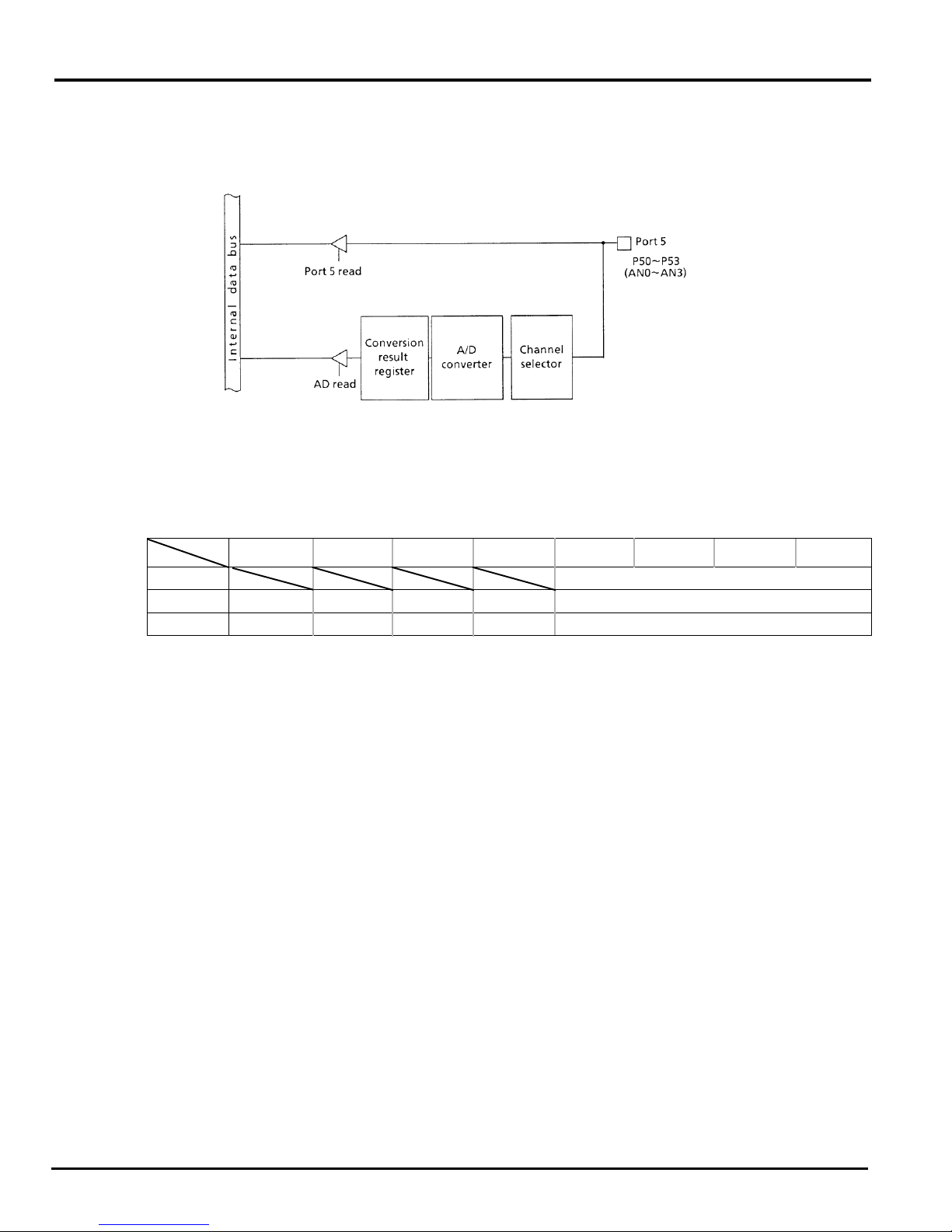
3.5.6 Port 5 (P50 - P53)
Port 5 is a 4-bit input port, also used as an analog input pin.
Figure 3.5 (11). Port 5
Port 5 Register
76543210
P5
(000DH)
Note: The input channel selection of A/D Converter is set by A/D Converter mode register ADMOD2.
bit Symbol P53 P52 P51 P50
Read/Write R
After reset Input mode
Figure 3.5 (12). Registers for Port 5
36
TOSHIBA CORPORATION
Page 37
TMP96C141AF
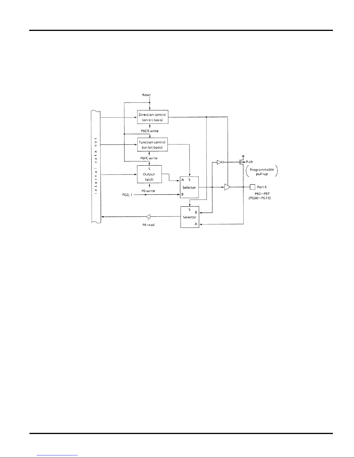
3.5.7 Port 6 (P60 - P67)
Port 6 is an 8-bit general-purpose I/O port. I/O can be set on
bit basis. Resetting sets Port 6 as an input port and connects
a pull-up resistor. It also sets all bits of the output latch to 1. In
addition to functioning as a general-purpose I/O port, Port 6
also functions as a pattern generator PG0/PG1 output. PG0 is
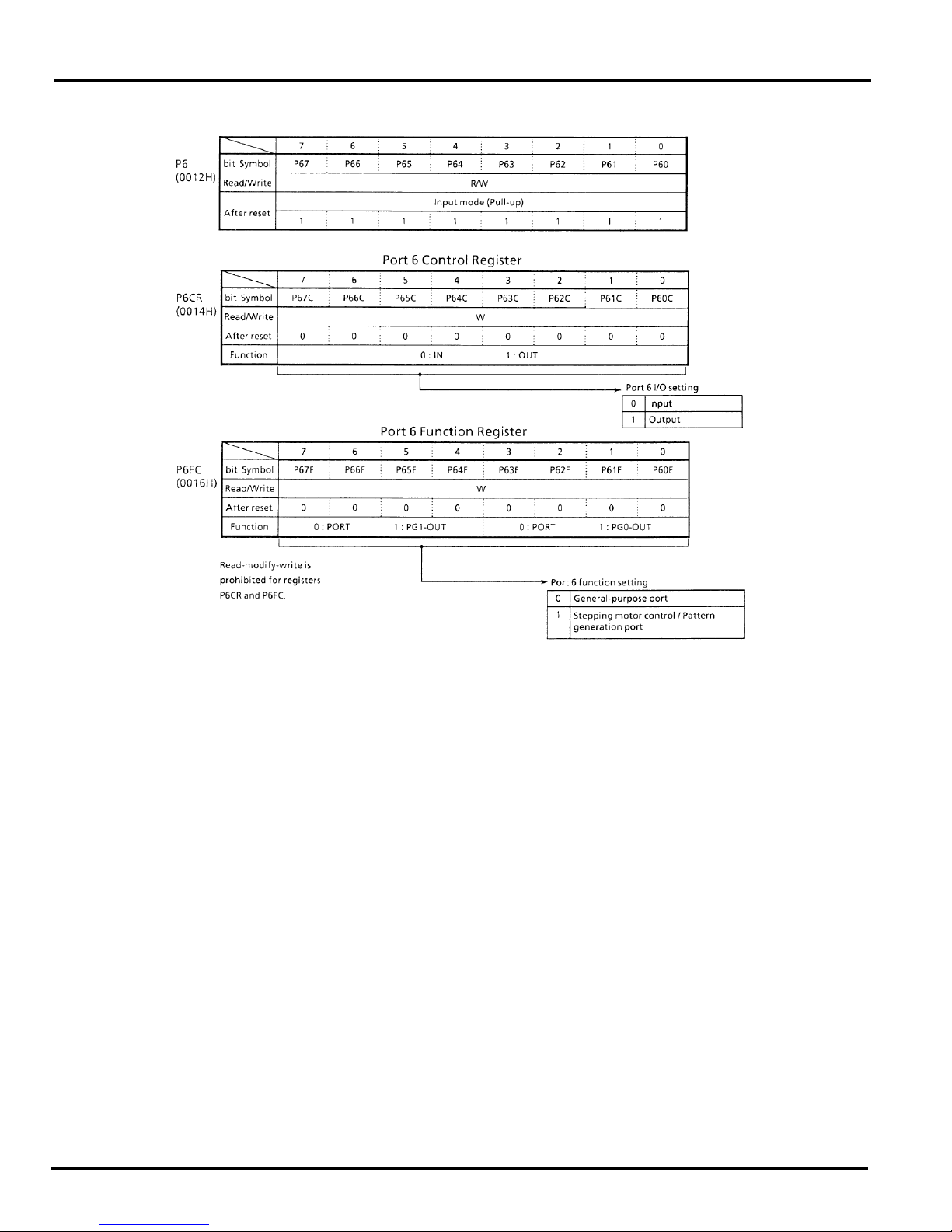
assigned to P60 to P63; PG1, to P64 to P67. Writing 1 in the
corresponding bit of the port 6 function register (P6FC)
enables PG output. Resetting resets the function register
P6FC value to 0, and sets all bits to ports.
Figure 3.5 (13). Port 6
TOSHIBA CORPORATION
37
Page 38
TMP96C141AF
Port 6 Register
Figure 3.5 (14). Registers for Port 6
38
TOSHIBA CORPORATION
Page 39
TMP96C141AF
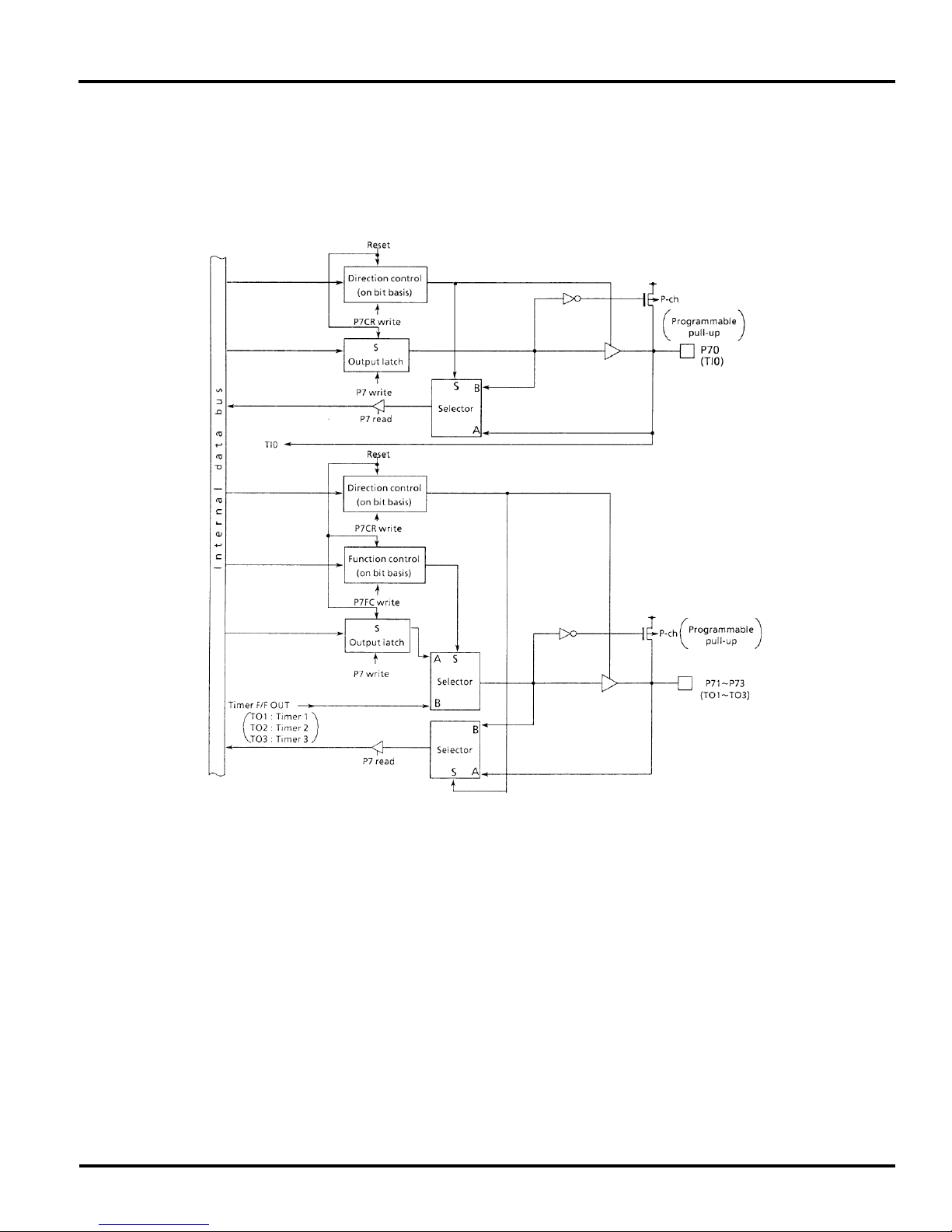
3.5.8 Port 7 (P70 - P73)
Port 7 is a 4-bit general-purpose I/O port. I/O can be set on bit
basis. Resetting sets Port 7 as an input port and connects a
pull-up resistor. In addition to functioning as a general-purpose
I/O port, Port 70 also functions as an input clock pin TI0; Port
71 as an 8-bit timer output (TO1), Port 72 as a PWM0 output
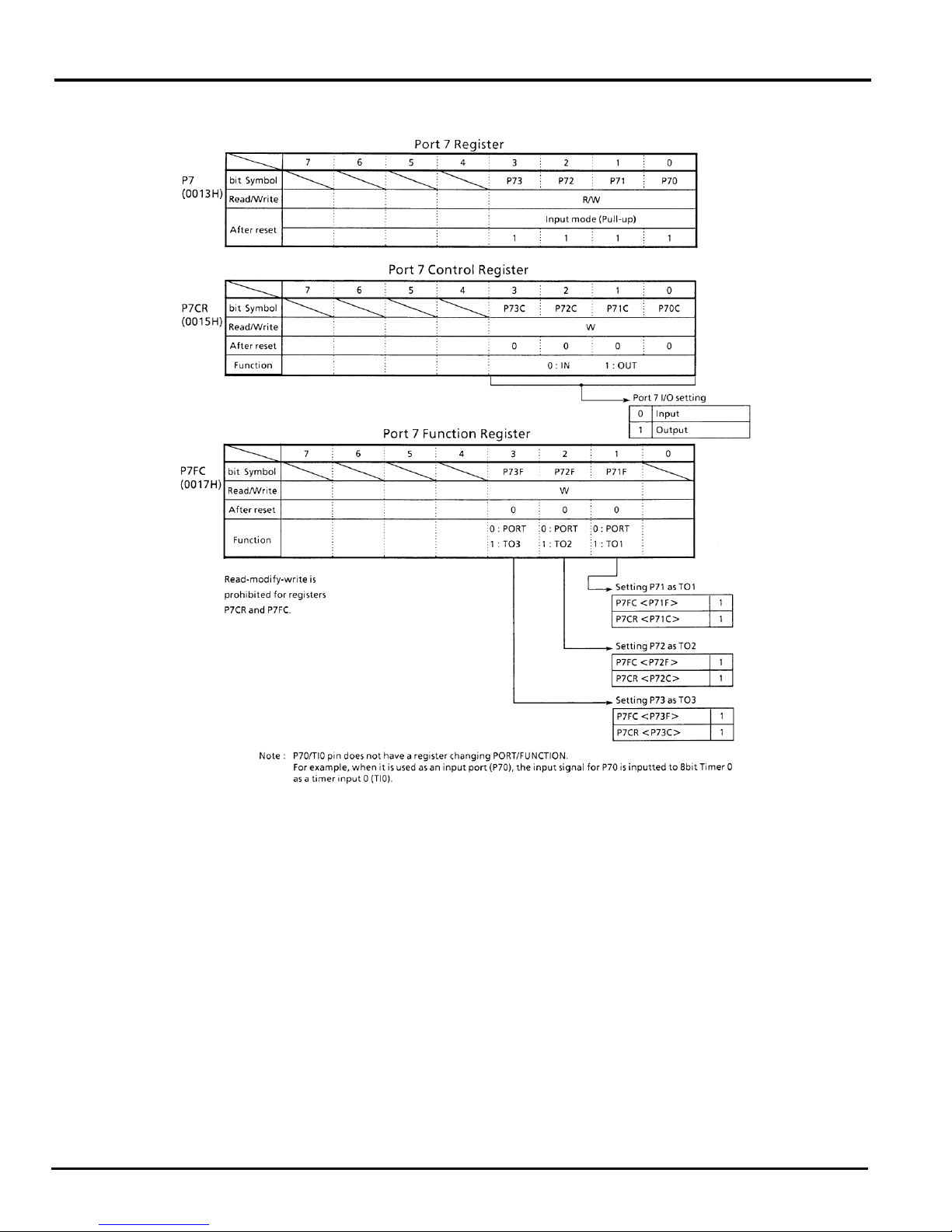
(TO2), and Port 73 as a PWM1 output (TO3) pin. Writing 1 in
the corresponding bit of the Port 7 function register (P7FC)
enables output of the timer. Resetting resets the function register P7FC value to 0, and sets all bits to ports.
TOSHIBA CORPORATION
Figure 3.5 (15). Port 7
39
Page 40
TMP96C141AF
40
Figure 3.5 (16). Registers for Port 7
TOSHIBA CORPORATION
Page 41
TMP96C141AF
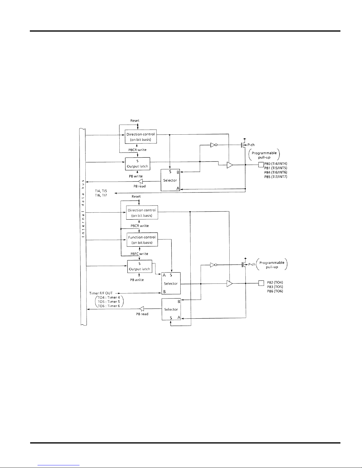
3.5.9 Port 8 (P80 - P83)
Port 8 is an 8-bit general-purpose I/O port. I/O can be set on a
bit basis. Resetting sets Port 8 as an input port and connects
a pull-up resistor. It also sets all bits of the output latch register
P8 to 1. In addition to functioning as a general-purpose I/O
port, Port 8 also functions as an input for 16-bit timer 4 and 5
(1) P80 ~ P86
clocks, an output for 16-bit timer F/F 4, 5 and 6 output, and an
input for INT0. Writing 1 in the corresponding bit of the Port 8
function register (P8FC) enables those functions. Resetting
resets the function register P8FC value to 0, and sets all bits to
ports.
TOSHIBA CORPORATION
Figure 3.5 (17). Port 8 (P80 - P86)
41
Page 42
TMP96C141AF
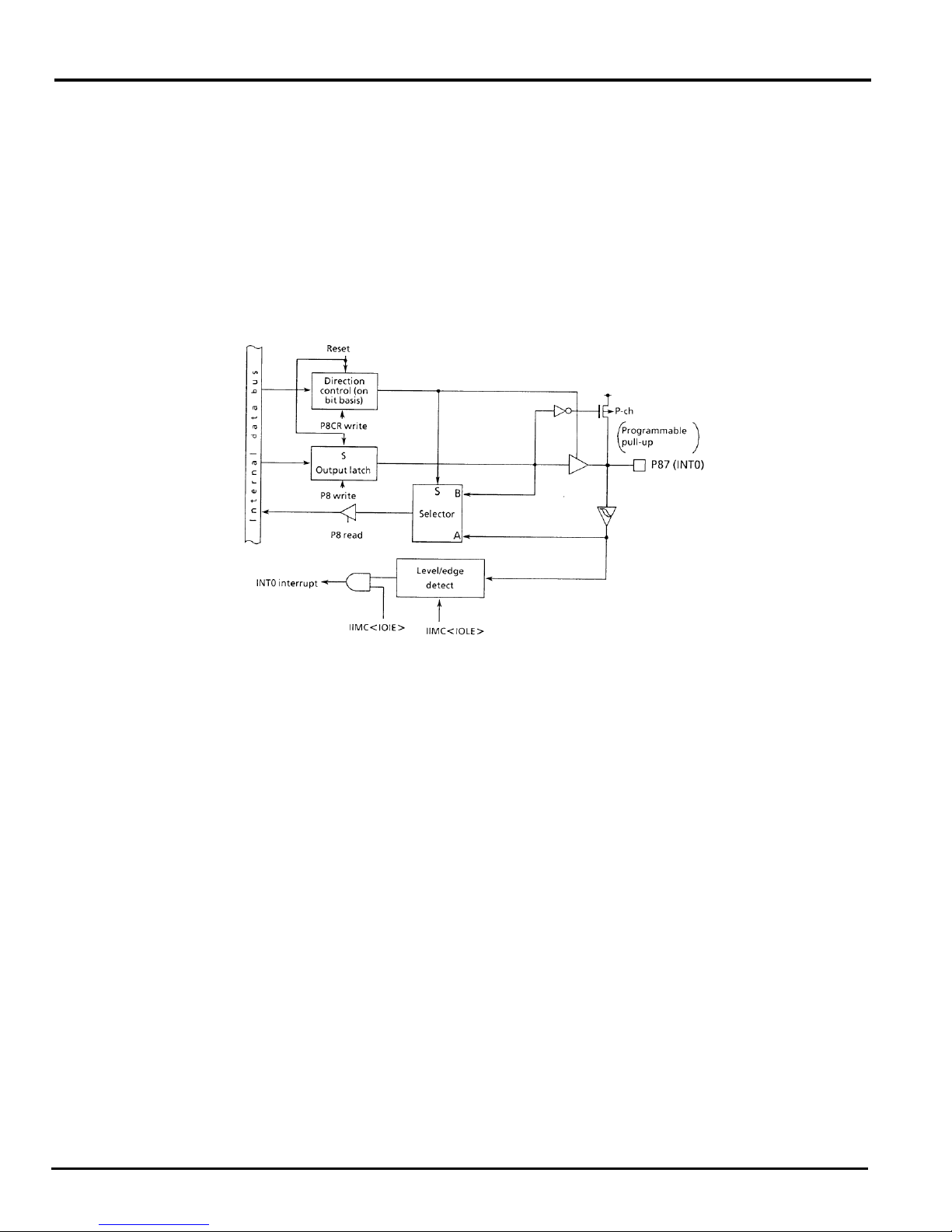
(2) P87 (INT0)
Port 87 is a general-purpose I/O port, and also used as
an INT0 pin for external interrupt request input.
42
Figure 3.5 (18). Port 87
TOSHIBA CORPORATION
Page 43
TMP96C141AF
TOSHIBA CORPORATION
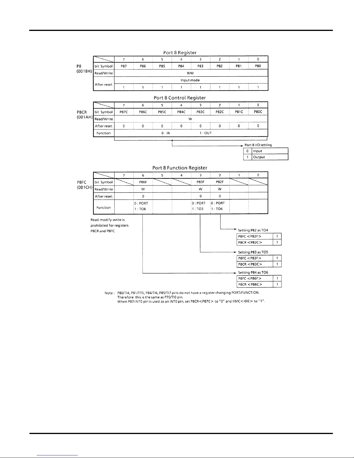
Figure 3.5 (19). Registers for Port 8
43
Page 44
TMP96C141AF
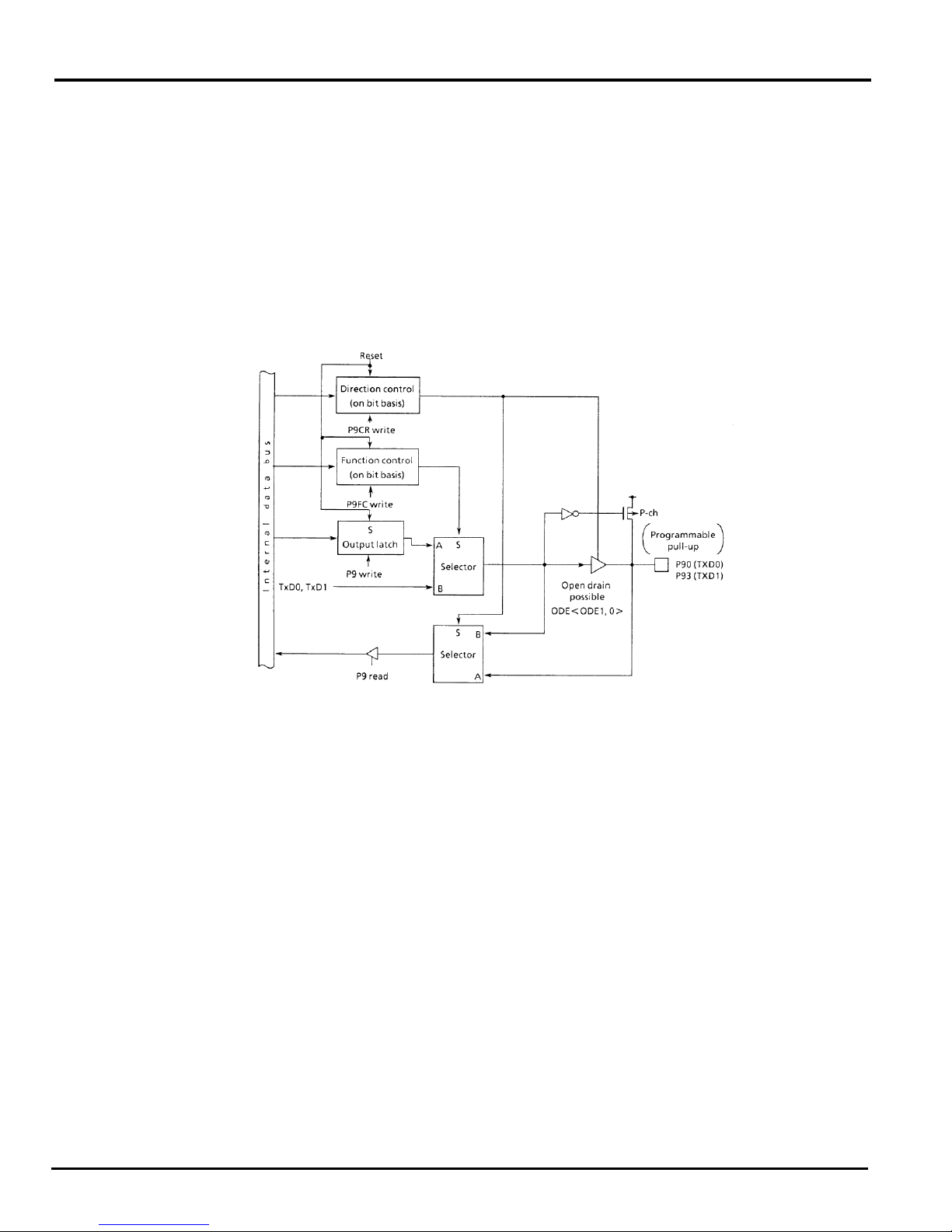
3.5.10 Port 9 (P90 - P95)
Port 9 is a 6-bit general-purpose I/O port. I/Os can be set on a
bit basis. Resetting sets Port 9 to an input port and connects a
pull-up resistor. It also sets all bits of the output latch register to
1.
In addition to functioning as a general-purpose I/O port, Port 9
can also function as an I/O for serial channels 0 and 1. Writing
1 in the corresponding bit of the port 9 function register (P9FC)
enables this function.
Resetting resets the function register value to 0 and sets
all bits to ports.
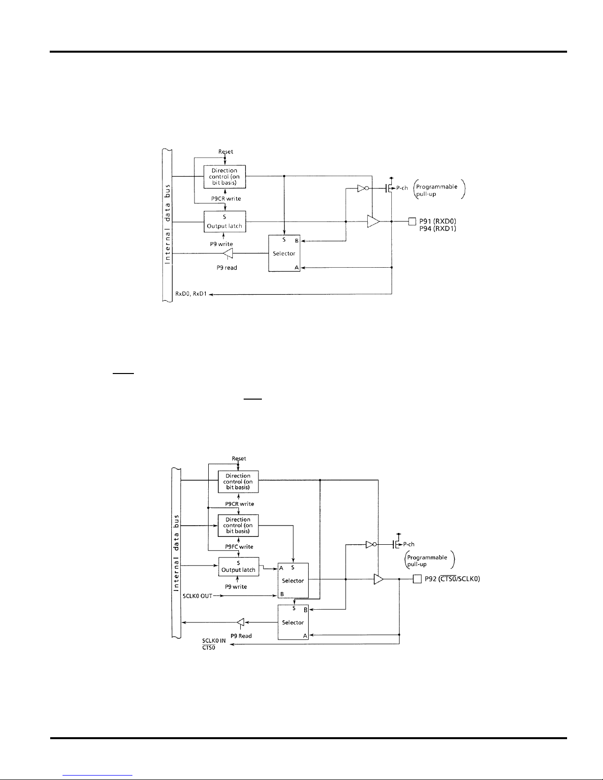
(1) Port 90 and 93 (TXD0/TXD1)
Ports 90 and 93 also function as serial channel TXD
output pins in addition to I/O ports.
They have a programmable open drain function.
44
Figure 3.5 (20). Ports 90 and 93
TOSHIBA CORPORATION
Page 45
TMP96C141AF
(2) Ports 91 and 94 (RXD0, 1)
Ports 91 and 94 are I/O ports, and also used as RXD
input pins for serial channels.
Figure 3.5 (21). Ports 91 and 94
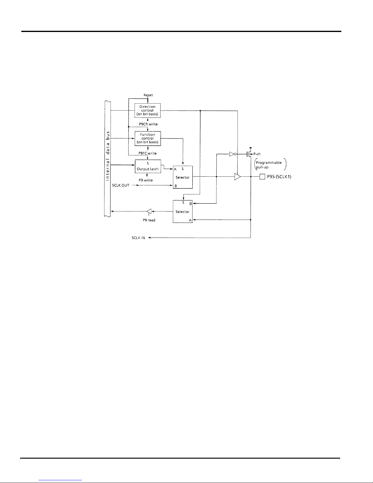
(3) Port 92 (CTS/
SCKL0)
Port 92 is an I/O port. It is also used as a CTS input pin
for serial channel0; additionally, the CTS0 pin, and also
as a SCKL0 I/O pin.
TOSHIBA CORPORATION
Figure 3.5 (22). Port 92
45
Page 46
TMP96C141AF
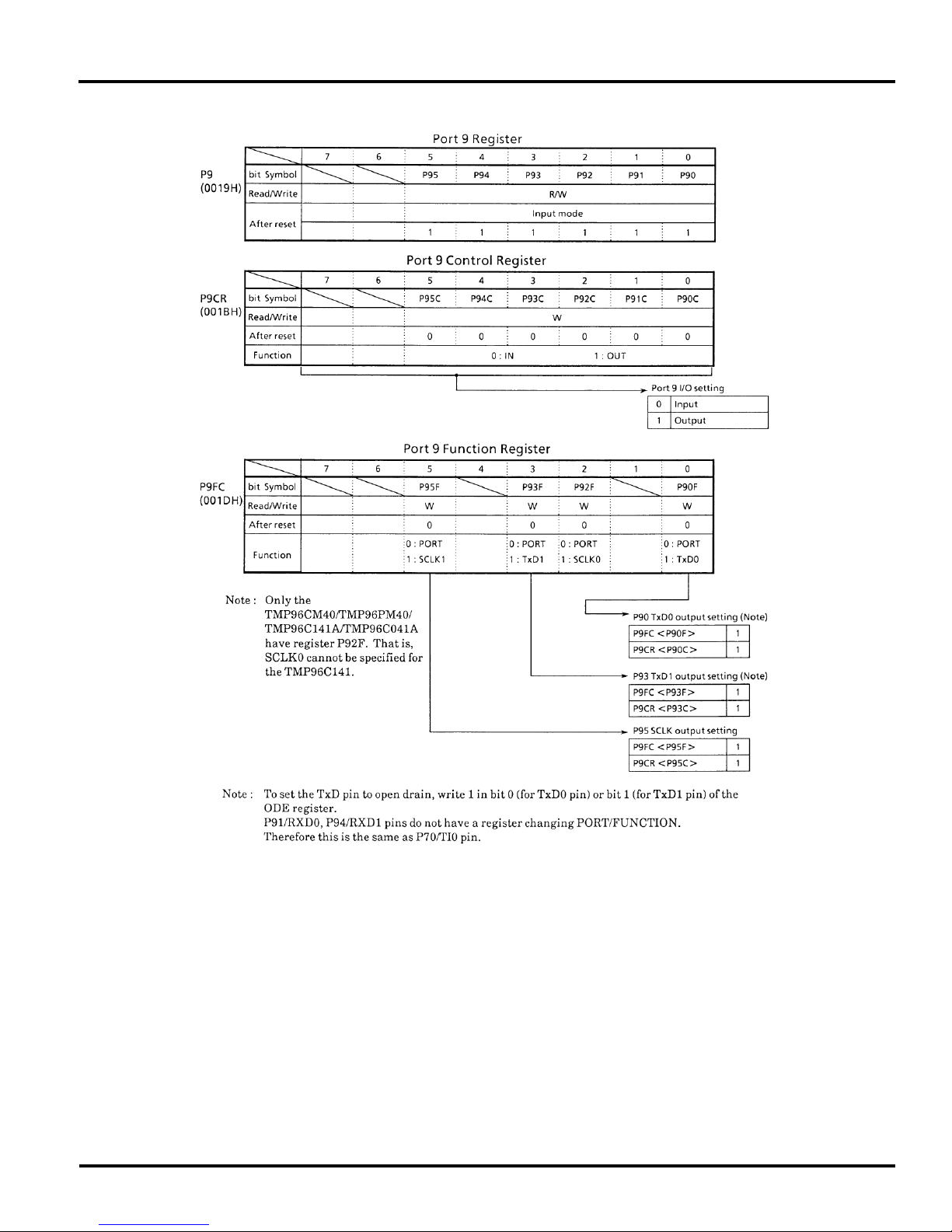
(4) Port 95 (SCLK)
Port 95 is a general-purpose I/O port. It is also used as
an SCLK I/O pin for serial channel 1.
46
Figure 3.5 (23). Port 95
TOSHIBA CORPORATION
Page 47
TMP96C141AF
TOSHIBA CORPORATION
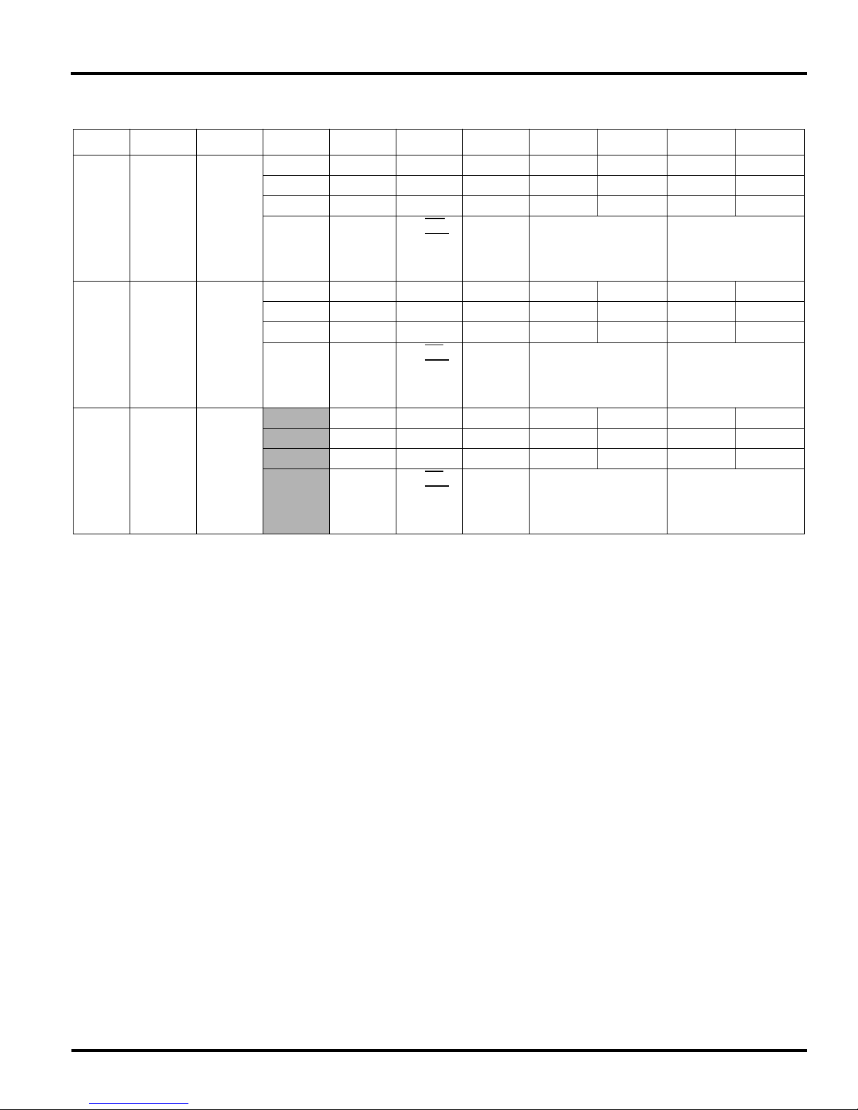
Figure 3.5 (24). Registers for Port 9
47
Page 48

TMP96C141AF
3.6 Chip Select/Wait Control
TMP96C141AF has a built-in chip select/wait controller used
to control chip select (CS0
- CS2 pins), wait (WAIT pin), and
data bus size (8 or 16 bits) for any of the three block address
areas.
3.6.1 Control Registers
Table 3.6 (1) shows control registers
One block address areas are controlled by 1-byte CS/
WAIT control registers (B0CS, B1CS, and B2CS). Registers
can be written to only when the CPU is in system mode. (There
are two CPU modes: system and normal.) The reason is that
the settings of these registers have an important effect on the
system.
(1) Enable
Control register bit 7 (B0E, B1E, and B2E) is a master
bit used to specify enable (1)/disable (0) of the setting.
Resetting B0E and B1E to disable (0) and B2E to
enable (1).
(2) System only specification
Control register bit 6 (B0SYS, B1SYS, and B2SYS) is
used to specify enable/disable of the setting depending on the CPU operating mode (system or normal).
Setting this bit to 0 enables setting (Address space for
, Wait state, Bus size, etc.) regardless of the CPU
CS
operating mode; setting it to 1 enables setting in system mode but disables setting in normal mode.
Resetting clears bit 6 to 0.
Bit 6 is mainly used when external memory data should
not be accessed in normal mode (i.e., for system mode
only memory data for the operating system).
(3) CS/CAS Waveform select
ister is used to specify data bus size. Setting this bit to
0 accesses the memory in 16-bit data bus mode; setting it to 1 accesses the memory in 8-bit data bus
mode.
Changing data bus size depending on the access
address is called dynamic bus sizing. Table 3.6 (2)
shows the details of the bus operation.
(5) Wait control
Control register bits 3 and 2 (B0W1, 0; B1W1, 0; B2W1,
0) are used to specify the number of waits. Setting these
bits to 00 inserts a 2-state wait regardless of the WAIT
pin status. Setting them to 01 inserts a 1-state wait
regardless of the WAIT status. Setting them to 10
inserts a 1-state wait and samples the WAIT pin status.
If the pin is low, inserting the wait maintains the bus
cycle until the pin goes high. Setting them to 11 completes the bus cycle without a wait regardless of the
WAIT pin status.
Resetting sets these bits to 00 (2-state wait mode).
(6) Address area specification
Control register bits 1 and 0 (B0C1, 0; B1C1, 0; B2C1,
0) are used to specify the target address area. Setting
these bits to 00 enables settings (CS output, Wait
state, Bus size, etc.) as follows:
* CS0 setting enabled when 7F00H to 7FFFH is
accessed.
* CS1 setting enabled when 480H to 7FFFH is
accessed.
* CS2 setting enabled when 8000H to 3FFFFFFH is
accessed, for the TMP96C141, which does not have a
built-in ROM.
Control register bit 5 (B0CAS, B1CAS, and B2CAS) is
used to specify waveform mode output from the chip
select pin (CS0/CAS0 - CS2/CAS2). Setting this bit to
0 specifies CS0 to CS2 waveforms; setting it to 1
specifies CAS0 to CAS2 waveforms.
Resetting clears bit 5 to 0.
(4) Data bus size select
Bit 4 (B0BUS, B1BUS, and B2BUS) of the control reg-
48
CS2 setting enabled when 10000H to 3FFFFFH is
accessed for the TMP96CM40/TMP96PM40, which
has built-in
ROM/PROM
Setting bits to 01 enables setting for all CS’s blocks
and outputs a low strobe signal (CS0/CAS0 ~ CS2/
CAS2) from chip select pins when 400000H to
7FFFFFH is accessed. Setting bits to 10 enables them
800000H to BFFFFFH is accessed. Setting bits to 11
enables them when C00000H to FFFFFFH is
accessed.
TOSHIBA CORPORATION
Page 49
TMP96C141AF
Table 3.6 (1) Chip Select/Wait Control Register
Code Name Address 76543210
B0E B0SYS B0CAS B0BUS B0W1 B0W0 B0C1 B0C0
WWWWWWWW
00000000
1 : CS/CAS
Enable
1 : SYSTEM
only
0 : CSO
1 : CAS0
0 : 16-bit
Bus
1 : 8-bit
Bus
00 : 2WAIT
01 : 1WAIT
10 : 1WAIT + n
11 : 0WAIT
00 : 7F00H ~ 7FFFH
01 : 400000H ~
10 : 800000H ~
11 : C00000H ~
B1E B1SYS B1CAS B1BUS B1W1 B1W0 B1C1 B1C0
WWWWWWWW
00000000
1 : CS/CAS
Enable
1 : SYSTEM
only
0 : CS1
1 : CAS1
0 : 16-bit
Bus
1 : 8-bit
Bus
00 : 2WAIT
01 : 1WAIT
10 : 1WAIT + n
11 : 0WAIT
00 : 480H ~ 7FFFH
01 : 400000H ~
10 : 800000H ~
11 : C00000H ~
B2E B2SYS B2CAS B2BUS B2W1 B2W0 B2C1 B2C0
WWWWWWWW
10000000
1 : CS/CAS
Enable
1 : SYSTEM
only
0 : CS2
1 : CAS2
0 : 16-bit
Bus
1 : 8-bit
Bus
00 : 2WAIT
01 : 1WAIT
10 : 1WAIT +n
11 : 0WAIT
00 : 8000H ~
01 : 400000H ~
10 : 800000H ~
11 : C00000H ~
B0CS
B1CS
B2CS
Block0
CS/WAIT
control
register
Block1
CS/WAIT
control
register
Block2
CS/WAIT
control
register
0068H
0069H
006AH
Note: With only block 2, enable (16-bit data bus, 2-wait mode) after reset.
TOSHIBA CORPORATION
49
Page 50
TMP96C141AF
Operand
Data Size
8 bits
16 bits
32 bits
Operand
Start Address
2n + 0
(even number)
2n + 1
(odd number)
2n + 0
(even number)
2n + 1
(odd number)
2n + 0
(even number)
2n + 1
(odd number)
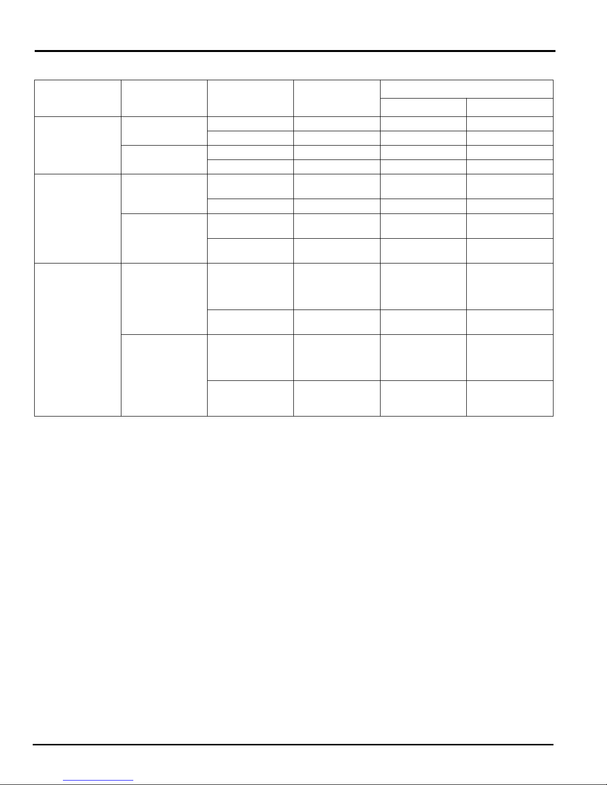
Table 3.6 (2) Dynamic Bus Sizing
Memory
Data Size
CPU Address
D15 - D8 D7 - D0
8 bits 2n + 0 xxxxx b7 - b0
16 bits 2n + 0 xxxxx b7 - b0
8 bits 2n + 1 xxxxx b7 - b0
16 bits 2n + 1 b7 - b0 xxxxx
8 bits
2n + 0
2n + 1
xxxxx
xxxxx
16 bits 2n + 0 b15 - b8 b7 - b0
8 bits
16 bits
8 bits
16 bits
8 bits
16 bits
2n + 1
2n + 2
2n + 1
2n + 2
2n + 0
2n + 1
2n + 2
2n + 3
2n + 0
2n + 2
2n + 1
2n + 2
2n + 3
2n + 4
2n + 1
2n + 2
2n + 4
xxxxx
xxxxx
b7 - b0
xxxxx
xxxxx
xxxxx
xxxxx
xxxxx
b15 - b8
b31 - b24
xxxxx
xxxxx
xxxxx
xxxxx
b7 - b0
b23 - b16
xxxxx
CPU Data
b7 - b0
b15 - b8
b7 - b0
b15 - b8
xxxxx
b15 - b8
b7 - b0
b15 - b8
b23 - b16
b31 - b24
b7 - b0
b23 - b16
b7 - b0
b15 - b8
b23 - b16
b31 - b24
xxxxx
b15 - b8
b31 - b24
xxxxx: During a read, data input to the bus is ignored. At write, the bus is at high impedance and the write strobe signal remains non-active.
50
TOSHIBA CORPORATION
Page 51
TMP96C141AF
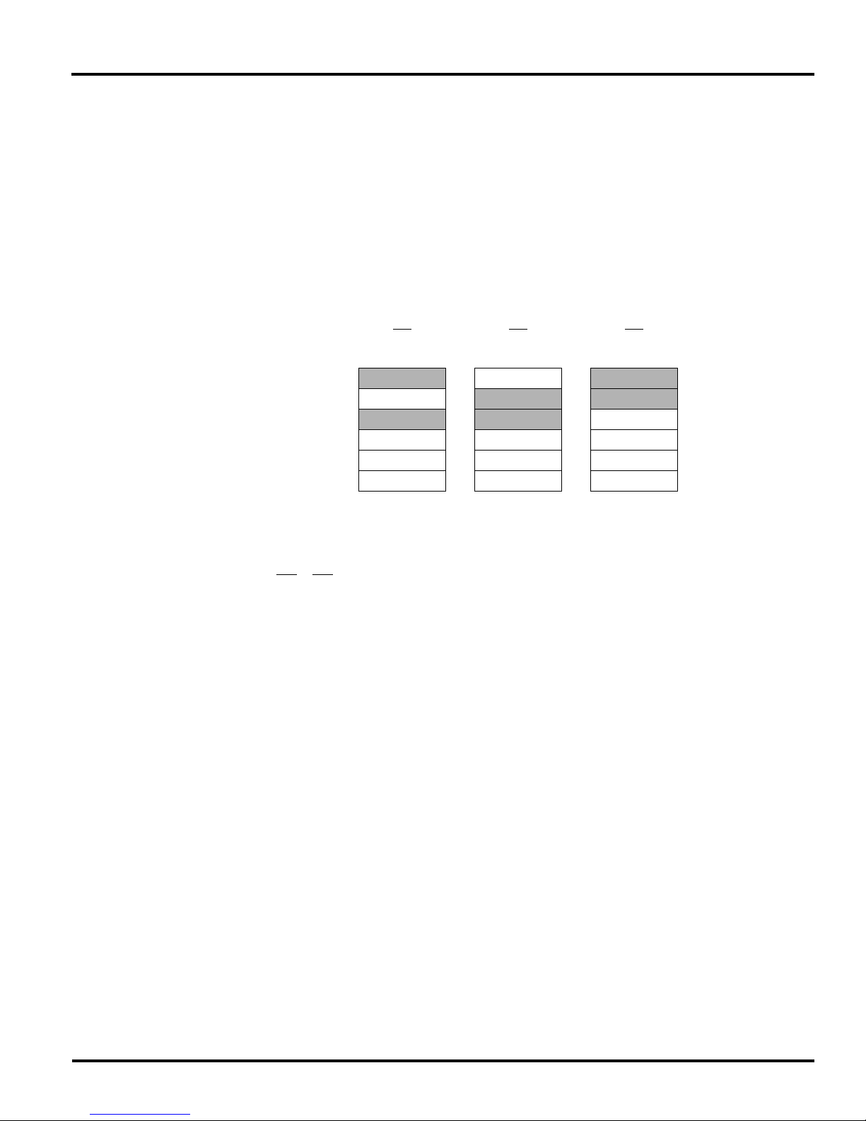
3.6.2 Chip Select Image
An image of the actual chip select is shown below. Out of the
whole memory area, address areas that can be specified are
divided into four parts. Addresses from 000000H to 3FFFFFH
are divided differently: 7F00H to 7FFFH is specified for CS0;
480H to 7FFFH, for CS1; and 8000H to 3FFFFFH, for CS2.
The reason is that a device other than ROM (i.e., RAM or I/O)
might be connected externally.
The addresses 7F00 to 7FFFH (256 bytes) for CS0 are
mapped mainly for possible expansions to external I/O.
The addresses 480H to 7FFFH (approximately 31K
CS0
000000H
7F00H
8000H B0C1, 0 = “00”
400000H B2C1, 0 = “00”
800000H B0C1, 0 = “01” B1C1, 0 = “01” B2C1, 0 = “01”
C00000H B0C1, 0 = “10” B1C1, 0 = “10” B2C1, 0 = “10”
FFFFFFH B0C1, 0 = “11” B1C1, 0 = “11” B2C1, 0 = “11”
(Mainly for I/O) (Mainly for RAM) (Mainly for ROM)
bytes) for CS1 are mapped there mainly for possible extensions to external RAM.
The addresses 8000H to 3FFFFFFH (approximately
4Mbytes) for CS2 are mapped mainly for possible extensions
to external ROM. After reset, CS2 is enabled in 16-bit bus and
2-wait. With the TMP96C141AF, which does not have a builtin ROM, the program is externally read at address 8000H in
this setting (16-bit bus, 2-wait). With the TMP96CM40F/
TMP96PM40F, which has a built-in ROM, addresses from
8000H to FFFFFH are used as the internal ROM area; CS2 is
disabled in this area. After reset, the CPU reads the program
from the built-in ROM in 16-bit bus, 0-wait mode.
CS1 CS2
B1C1, 0 = “00”
Supplement 1: Access priority is highest for built-in I/O, then built-in memory, and lowest for the chip select/wait controller.
Supplement 2: External areas other than CS0
When using the chip select/wait controller, do not specify the same address area more than once. (However, when addresses 7F00H - 7FFFH
for CS0 and 480H - 7FFFH for CS1 are specified, in other words, specifications overlap, only the CS0 setting/pin is active.)
to CS2 are accessed in 16-bit data bus (0 wait) mode.
TOSHIBA CORPORATION
51
Page 52
TMP96C141AF
3.6.3 Example of Usage
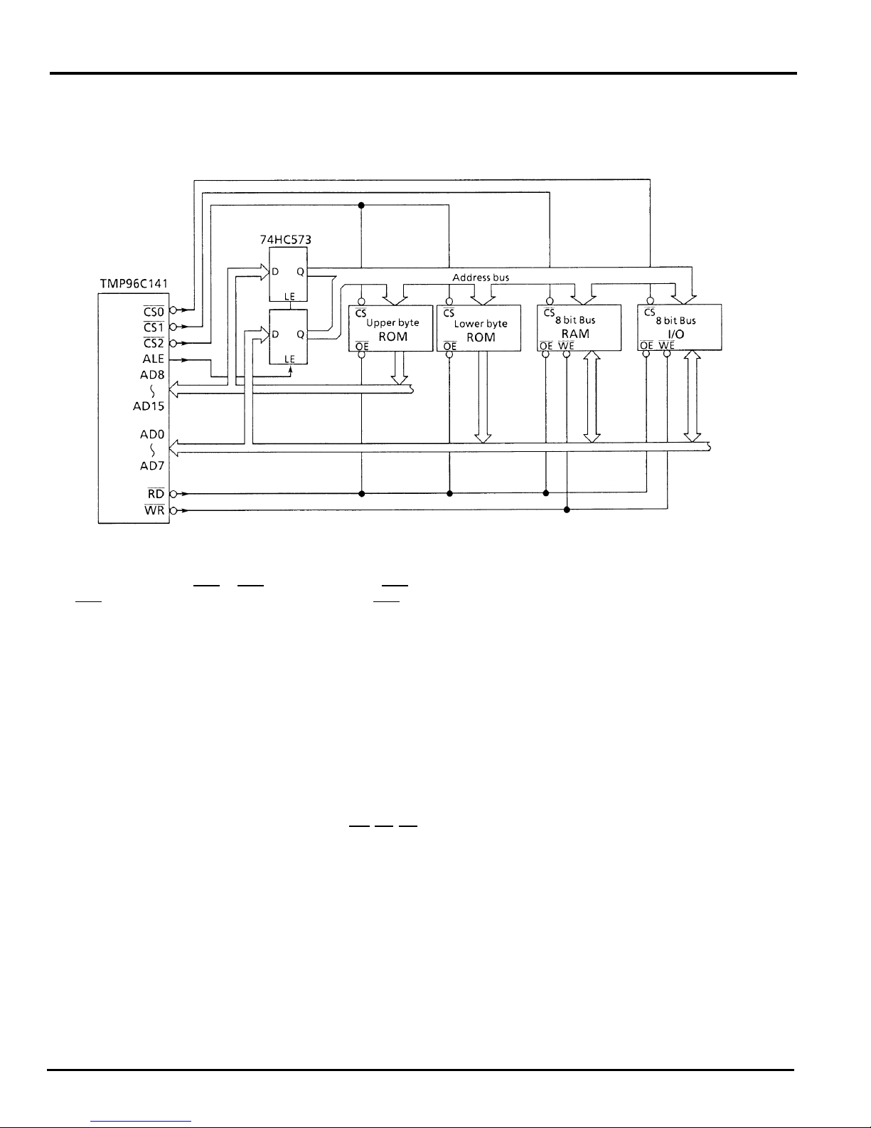
Figure 3.6 (1) is an example in which an external memory is con-
nected to the TMP96C141AF. In this example, a ROM is connected using 16-bit Bus; a RAM is connected using 8-bit Bus.
Figure 3.6 (1). Example of External Memory Connection (ROM = 16 bits, RAM and I/O = 8 bits)
Resetting sets pins CS0
to CS2 to input port mode. CS0
and CS1 are set high due to an internal pull-up resistor; CS2,
P4CR EQU 0EH
P4FC EQU 10H
B0CS EQU 68H
B1CS EQU 69H
B2CS EQU 6AH
LD (BOCS), 90H ; CS0 = 8 bits, 2WAIT, 7F00H ~ 7FFFH
LD (B1CS), 9CH ; CS1 = 8 bits, 0WAIT, 480H ~ 7EFFH
LD (B2CS), 84H ; CS2 = 16 bits, 1WAIT, 8000H ~ 3FFFFFH
LD (P4CR), 07H
LD (P4FC), 07H
CSO
, CS1, CS2 output mode setting
)
low due to an internal pull-down resistor. The program used to
set these pins is as follows:
52
TOSHIBA CORPORATION
Page 53
TMP96C141AF
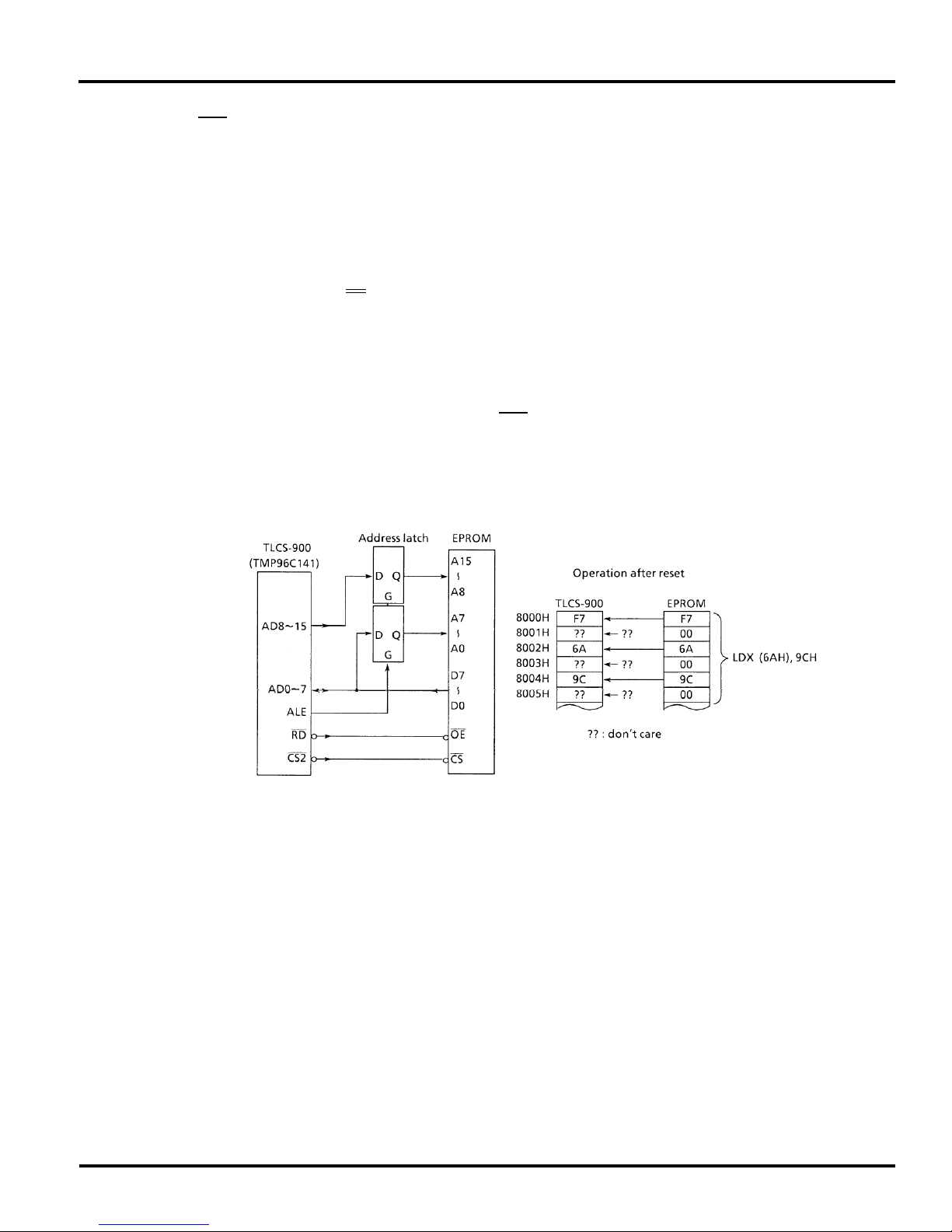
3.6.4 How to Start with an 8-Bit Data Bus
Resetting sets the CS2
pin low due to an internal pull-down
resistor; memory access starts in 16-bit data bus (2-wait)
B2CS EQU 6AH ; CS2 register address
ORG 8000H ; RESET address
LDX (B2CS), 9CH ; CS2 8-bit, 0WAIT, 8000H ~
After reset, the program reads the LDX (B2CS), 9CH
instruction in 16-bit data bus mode. LDX is a 6-byte instruction: the 2nd, 4th and 6th bytes are handled as dummies (i.e.,
only codes in the 1st, 3rd and 5th bytes are actually used).
Even if starting in 8-bit data bus mode, it is possible to program so that the LDX instruction is executed and the block 2
mode. To start in 8-bit data bus mode, a special operation is
required. Operation is as described in the example below:
area (8000H - 3FFFFFH) is accessed in 8-bit data bus mode
without any problem.
The above program does not include setting the P42/
pin to output; add a program to set the P4CR and P4FC
CS2
registers as required.
TOSHIBA CORPORATION
53
Page 54

TMP96C141AF
3.7 8-bit Timers
The TMP96C141AF contains two 8-bit timers (timers 0 and 1),
each of which can be operated independently. The cascade
connection allows these timers to be used as 16-bit timer. The
following four operating modes are provided for the 8-bit timers.
• 8-bit interval timer mode (2 timers)
• 16-bit interval timer mode (1 timer)
• 8-bit programmable square wave pulse generation (PPG :
variable duty with variable cycle) output mode (1 timer)
• 8-bit pulse width modulation (PWM: variable duty with con-
stant cycle) output mode (1 timer)
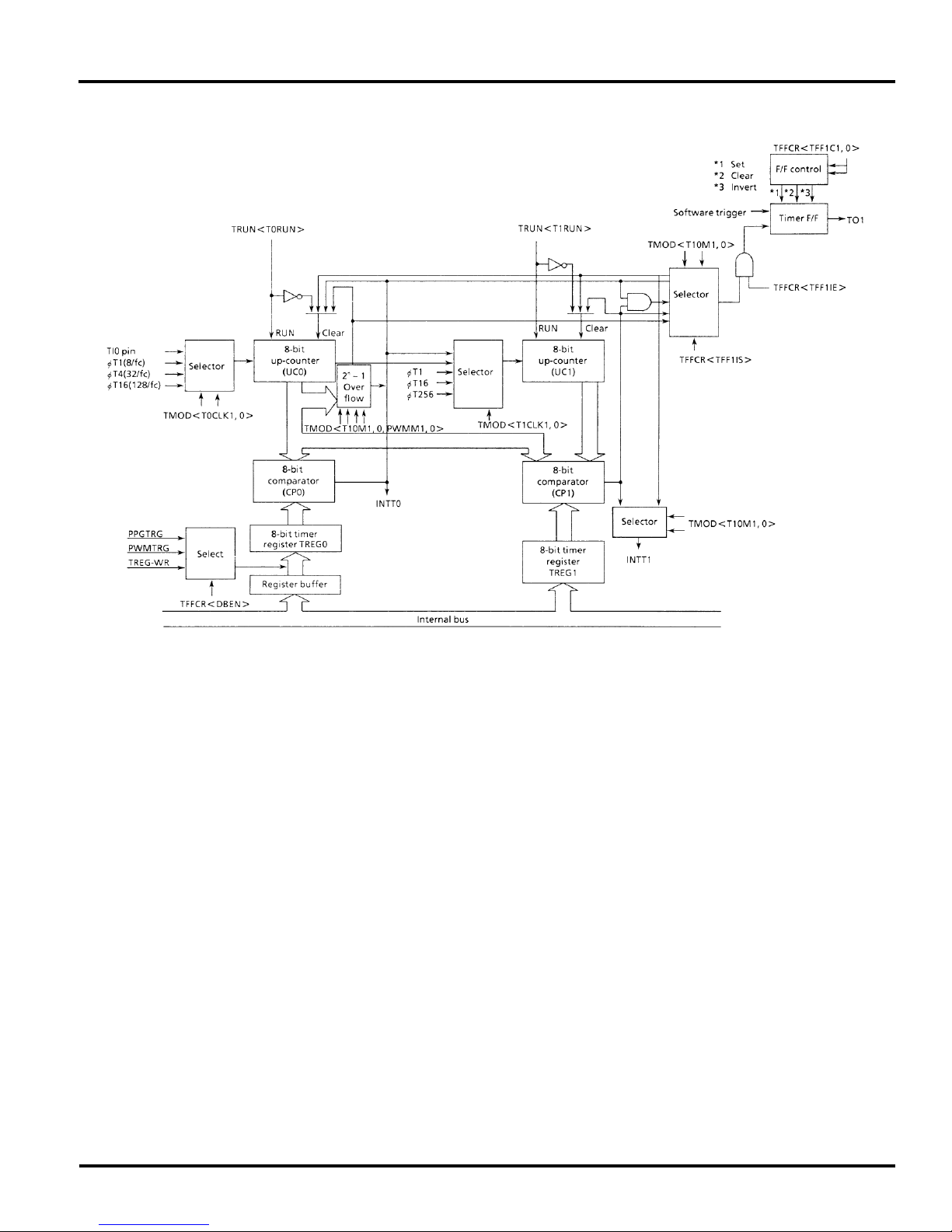
Figure 3.7 (1) shows the block diagram of 8-bit timer
(timer 0 and timer 1).
Each interval timer consists of an 8-bit up-counter, 8-bit
comparator, and 8-bit timer register. Besides, one timer flipflop (TFF1) is provided for pair of timer 0 and timer 1.
Among the input clock sources for the interval timers, the
internal clocks of
φ
T1,
φ
T4,
φ
T16, and
φ
T256 are obtained
from the 9-bit prescaler shown in Figure 3.7 (2).
The operation modes and timer flip-flops of the 8-bit
timer are controlled by three control registers TMOD, TFFCR,
and TRUN.
54
TOSHIBA CORPORATION
Page 55
TMP96C141AF
Figure 3.7 (1). Block Diagram of 8-Bit Timers (Timers 0 and 1)
TOSHIBA CORPORATION
55
Page 56
TMP96C141AF
➀
➁
Prescaler
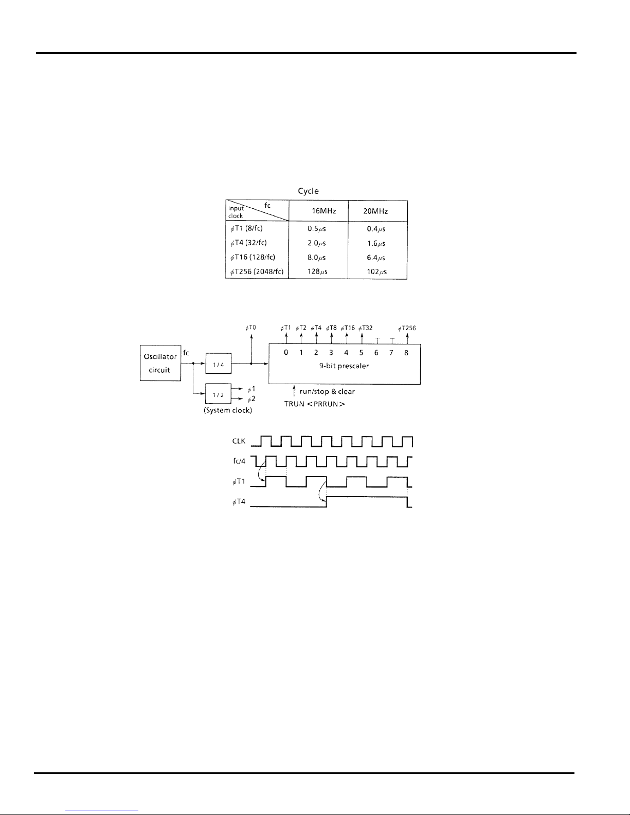
This 9-bit prescaler generates the clock input to the 8bit timers, 16-bit timer/event counters, and baud rate
generators by further dividing the fundamental clock
(fc) after it has been divided by 4 (fc/4).
Among them, 8-bit timer uses four types of clock:
φ
T1,
φ
T4,
φ
T16, and
φ
T256.
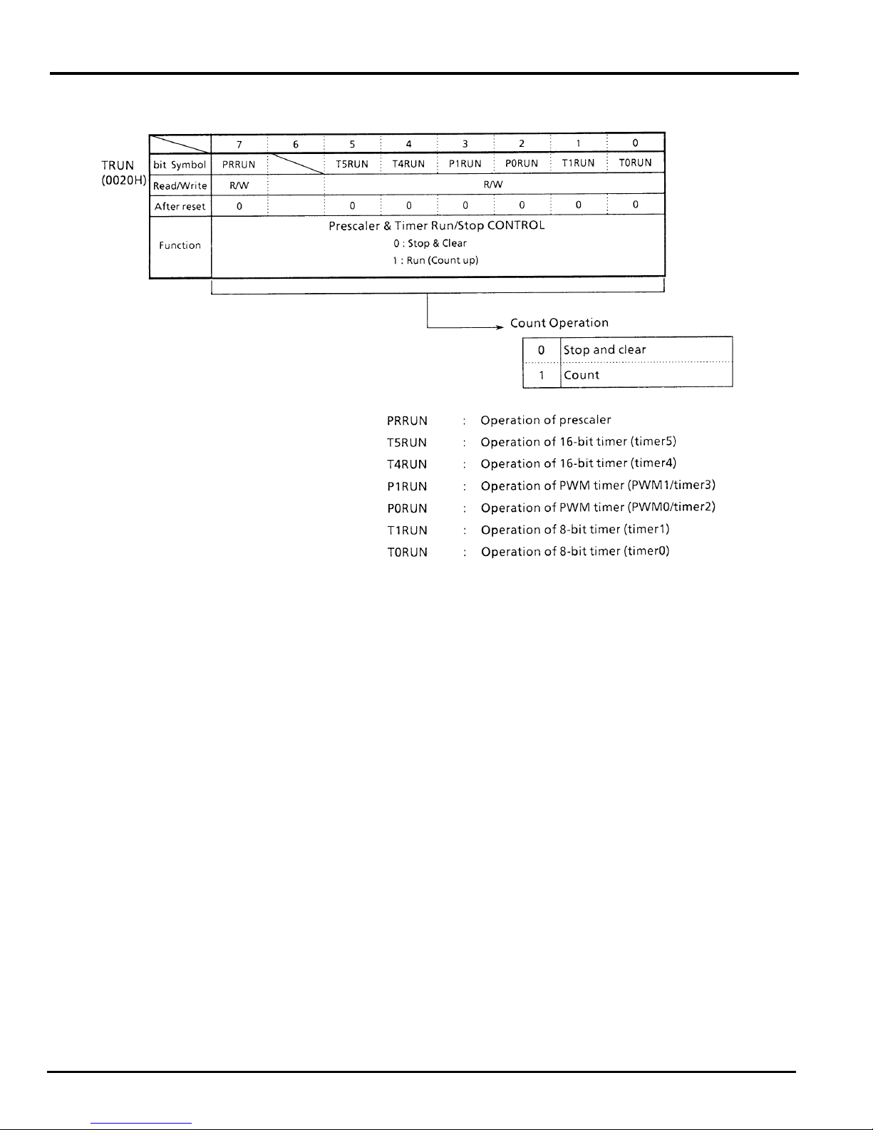
This prescaler can be run or stopped by the timer
operation control register TRUN <PRRUN>. Counting
starts when <PRRUN> is set to “1”, while the prescaler
is cleared to zero, and stops operation when
<PRRUN> is set to “0”. Resetting clears <PRRUN> to
“0”, which clears and stops the prescaler.
Up-counter
This is an 8-bit binary counter which counts up by the
input clock pulse specified by TMOD.
The input clock of timer 0 is selected from the external
clock from T10 pin and the three internal clocks
(8/fc),
φ
T4 (32/fc), and
φ
T16 (128/fc), according to the
set value of TMOD register.
The input clock of timer 1 differs depending on the
operation mode. When set to 16-bit timer mode, the
overflow output of timer 0 is used as the input clock.
When set to any other mode than 16-bit timer mode,
the input clock is selected from the internal clocks
(8/fc),
φ
T16 (128/fc), and
φ
T256 (2048/fc) as well as
the comparator output (match detection signal) of
timer 0 according to the set value of TMOD register.
56
Figure 3.7 (2). Prescaler
Example : When TMOD <T10M1, 0> = 01, the over
φ
T1
Operation mode is also set by TMOD register. When
reset, it is initialized to TMOD <T01M1, 0> = 00
whereby the up-counter is placed in the 8-bit timer
mode.
The counting and stop and clear of up-counter can be
φ
T1
controlled for each interval timer by the timer operation
control register TRUN. When reset, all up-counters will
be cleared to stop the timers.
flow output of timer 0 becomes the input
clock of timer 1 (16 bit timer mode).
When TMOD <T10M1, 0> = 00 and TMOD
<T1CLK1, 0> = 01,
φ
T1 (8/fc) becomes
the input of timer 1 (8 bit timer mode).
TOSHIBA CORPORATION
Page 57
➂
➃
⑤
TMP96C141AF
Timer register
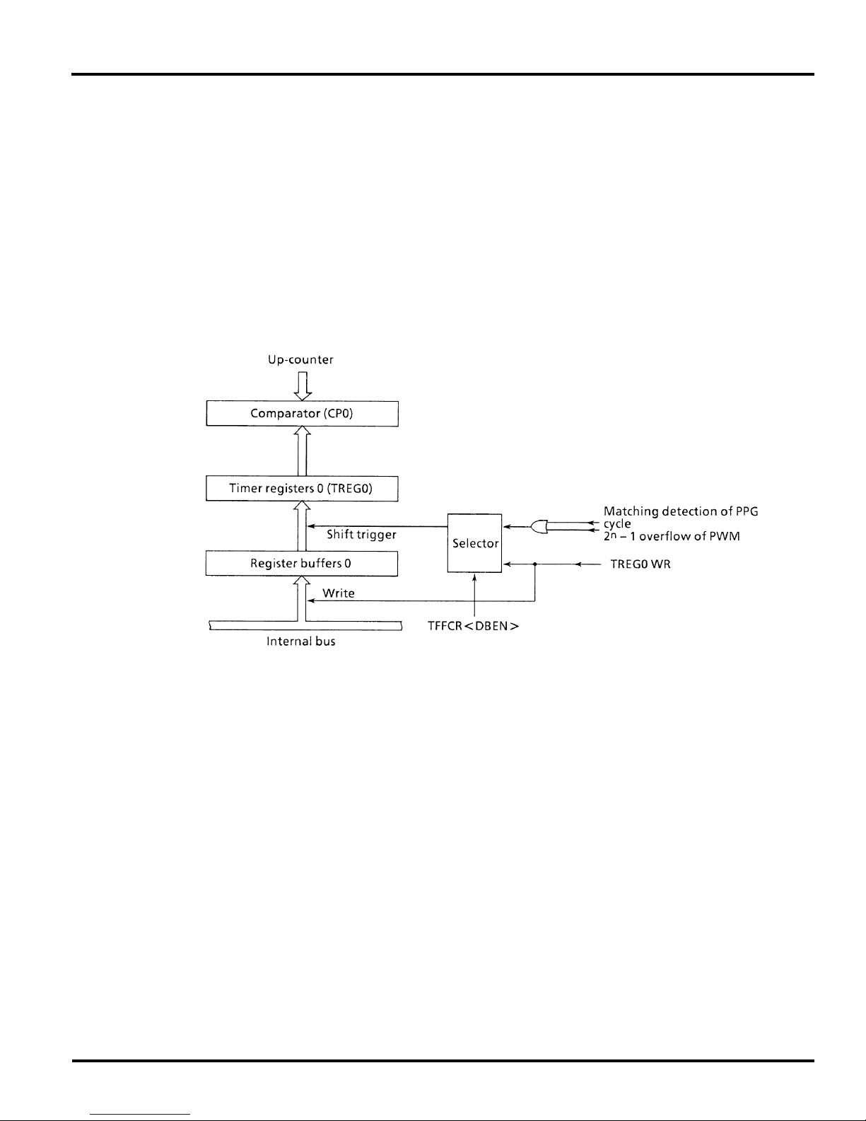
This is an 8-bit register for setting an interval time.
When the set value of timer registers TREG0, TREG1,
matches the value of up-counter, the comparator
match detect signal becomes active. If the set value is
00H, this signal becomes active when the up-counter
overflows.
Timer register TREG0 is of double buffer structure,
each of which makes a pair with register buffer.
The timer flip-flop control register TFFCR <DBEN> bit
controls whether the double buffer structure in the
TREG0 should be enabled or disabled. It is disabled
when <DBEN> = 0 and enabled when they are set to
1.
In the condition of double buffer enable state, the data
is transferred from the register buffer to the timer register when the 2
n
-1 overflow occurs in PWM mode, or at
the PPG cycle in PPG mode. Therefore, during timer
mode, the double buffer cannot be used.
When reset, it will be initialized to <DBEN> = 0 to disable the double buffer. To use the double buffer, write
data in the timer register, set <DBEN> to 1, and write
the following data in the register buffer.
Figure 3.7 (3). Configuration of Timer Register 0
Note : Timer register and the register buffer are allocated to the same
memory address. When <DBEN> = 0, the same value is written in
The memory address of each timer register is as follows.
TREG0: 000022H
TREG1: 000023H
All registers are write-only and cannot be read.
Comparator
A comparator compares the value in the up-counter
with the values to which the timer register is set. When
they match, the up-counter is cleared to zero and an
interrupt signal (INTT0, INTT1) is generated. If the timer
TOSHIBA CORPORATION
the register buffer as well as the timer register, while when <DBEN>
= 1 only the register buffer is written.
flip-flop inversion is enabled, the timer flip-flop is
inverted at the same time.
Timer flip-flop (timer F/F: TFF1)
The status of the timer flip-flop is inverted by the match
detect signal (comparator output) of each interval timer
and the value can be output to the timer output pins
TO1 (also used as P71).
A timer F/F is provided for a pair of timer 0 and timer 1
and is called TFF1. TFF1 is output to TO1 pin.
57
Page 58
TMP96C141AF
Figure 3.7 (4). Timer Operation Control Register (TRUN)
58
TOSHIBA CORPORATION
Page 59
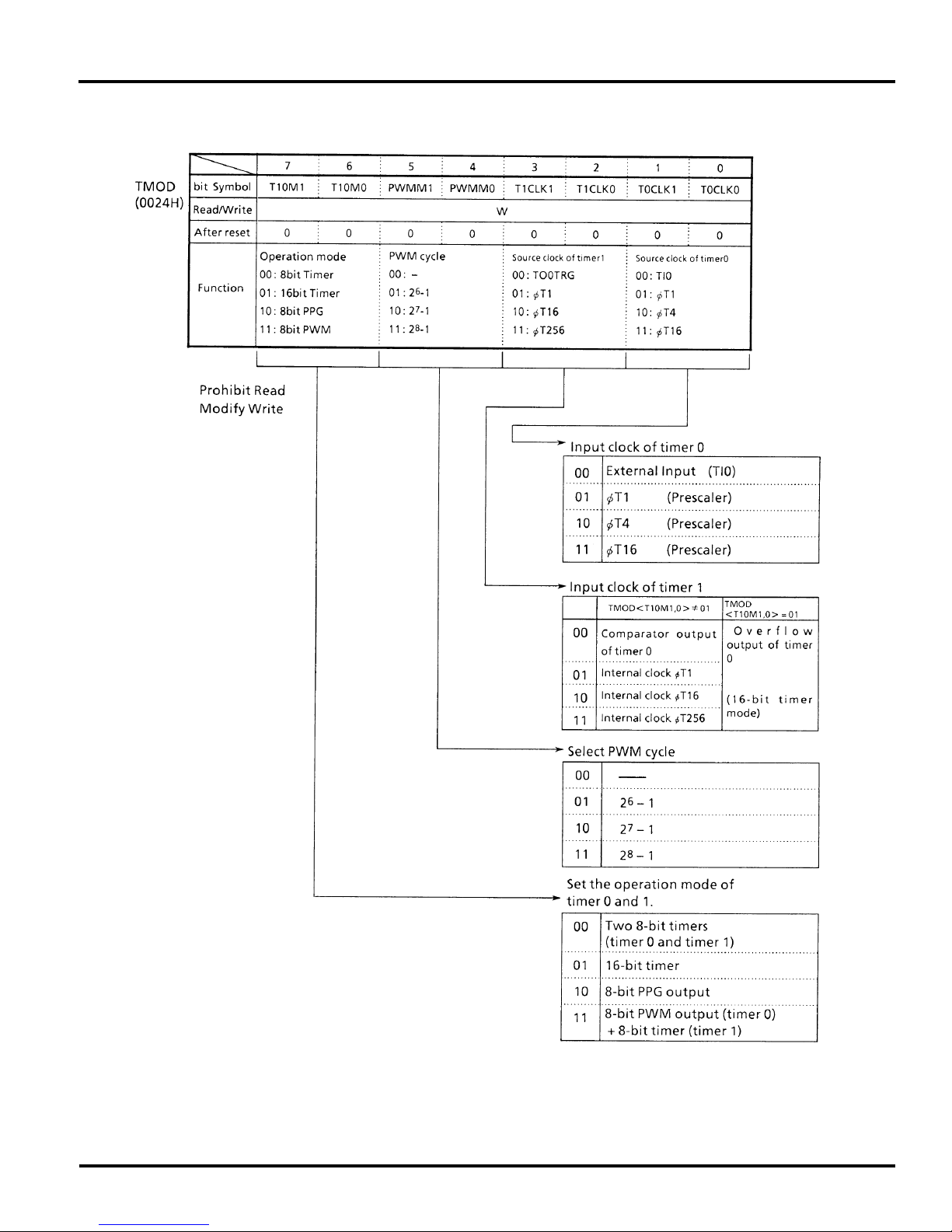
TMP96C141AF
Figure 3.7 (5). Timer Mode Control Register (TMOD)
TOSHIBA CORPORATION
59
Page 60
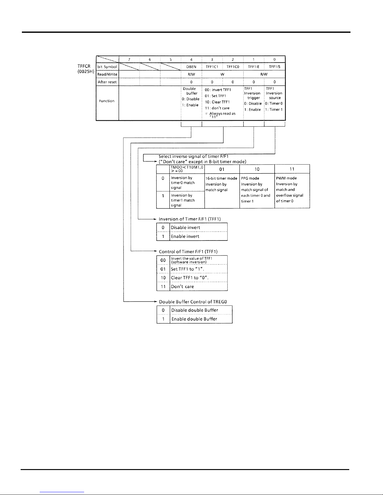
TMP96C141AF
Figure 3.7 (6). Timer Flip-Flop Control Register (TFFCR)
60
TOSHIBA CORPORATION
Page 61
←
←
←
➀
TMP96C141AF
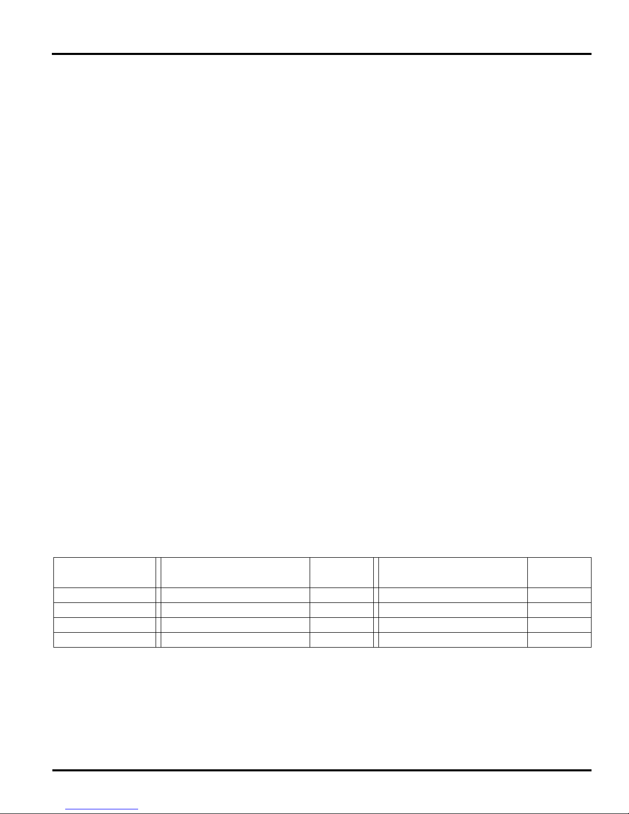
The operation of 8-bit timers will be described below:
(1) 8-bit timer mode
Two interval timers 0, 1, can be used independently as
8-bit interval timer. All interval timers operate in the
same manner, and thus only the operation of timer 1
will be explained below.
MSB LSB
76543210
TRUN
TMOD
–x––––0– Stop timer 1, and clear it to “0”.
0 0 x x 0 1 – – Set the 8-bit timer mode, and select
Generating interrupts in a fixed cycle
To generate timer 1 interrupt at constant intervals using
timer 1 (INTT1), first stop timer 1 then set the operation
mode, input clock, and a cycle to TMOD and TREG1
register, respectively. Then, enable interrupt INTT1 and
start the counting of timer 1.
Example: To generate timer 1 interrupt every 40
microseconds at fc = 16 MHz, set each
register in the following manner.
φ
T1 (0.5 µ s @ fc = 16MHz) as the input clock.
TREG1 ← 01010000 Set the timer register at 40 µ s
φ
T1 = 50H.
INTET10 ← 1101–––– Enable INTT1, and set it to “Level 5”.
TRUN
Note: x; don’t care –; no change
1x ––––1– Start timer 1 counting.
Use the following table for selecting the input clock.
Table 3.7 (1) 8-Bit Timer Interrupt Cycle and Input Clock
Input Clock
φ
T1 (8/fc) 0.5 µ s ~ 128 µ s 0.5 µ s 0.4 µ s ~ 102.4 µ s 0.4 µ s
φ
T4 (32/fc) 2 µ s ~ 512 µ s2
φ
T16 (128/fc) 8 µ s ~ 2.048ms 8 µ s 6.4 µ s ~ 1.638ms 6.4 µ s
φ
T256 (2048/fc) 128 µ s ~ 32.708ms 128 µ s 102.4 µ s ~ 2.621ms 128 µ s
Note: The input clock of timer 0 and timer 1 are different from as follows:
Timer 0: T10 input,
Timer 1: Match Output of Timer 0,
φ
T1,
Interrupt Cycle
(at fc = 16MHz)
φ
T4,
φ
T16
φ
T1,
φ
T16,
φ
T256
Resolution
µ
s 1.6 µ s ~ 409.6 µ s 1.6 µ s
Interrupt Cycle
(at fc = 20MHz)
Resolution
TOSHIBA CORPORATION
61
Page 62
TMP96C141AF
➁
←
←
←
←
←
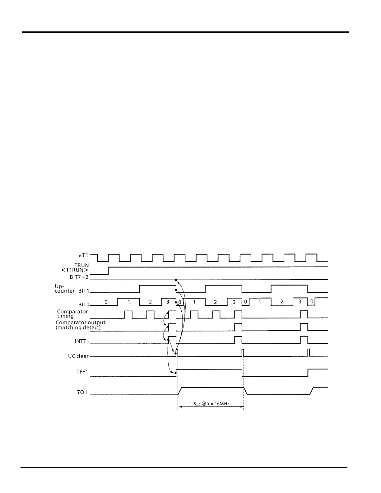
Generating a 50% duty square wave pulse
TO1 pin at fc = 16MHz, set each register in
the following procedures. Either timer 0 or
The timer flip-flop (TFF1) is inverted at constant intervals, and its status is output to timer output pin (TO1).
timer 1 may be used, but this example uses
timer 1.
Example: To output a 3.0 µ s square wave pulse from
76543210
TRUN
TMOD
TREG1 ← 00000011 Set the timer register at 3.0 µ s ÷
TFFCR ← ––––1011 Clear TFF1 to “0”, and set to invert by the match detect signal from timer 1.
P7CR
P7FC
TRUN
–x––––0– Stop timer 1, and clear it to “0”.
0 0 x x 0 1 – – Set the 8-bit timer mode, and select
φ
T1 ÷ 2 = 3.
xxxx––1–
xxxx––1x
1x ––––1– Start timer 1 counting.
Select P71 as TO1 pin.
)
φ
T1 (0.5 µ s @ fc = 16MHz) as the input clock.
Note: x; don’t care –; no change
Figure 3.7 (7). Square Wave (50% Duty) Output Timing Chart
62
TOSHIBA CORPORATION
Page 63
TMP96C141AF
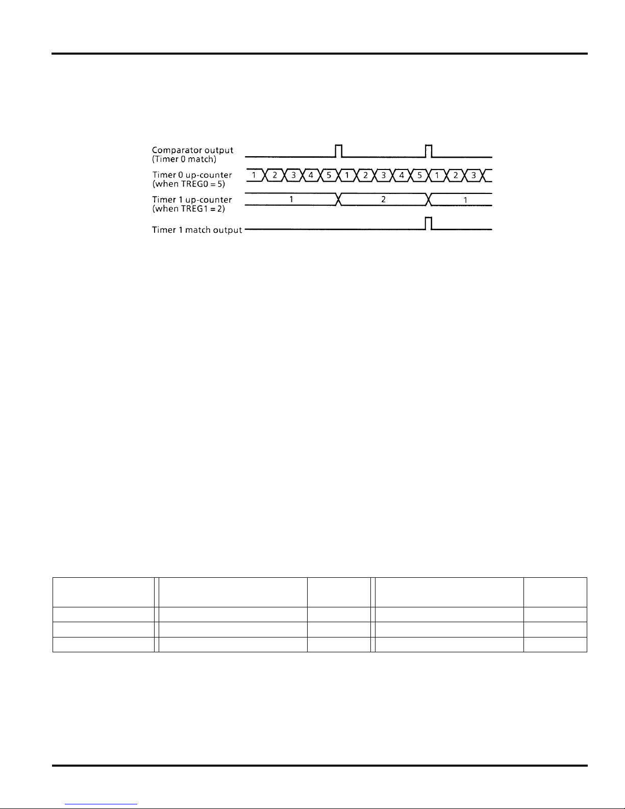
➂ Making timer 1 count up by match signal from timer
0 comparator
Figure 3.7 (8). Timer 1 Count Up by Timer 0
➃ Output inversion with software
The value of timer flip-flop (TFF1) can be inverted, independent of timer operation.
Writing “00” into TFFCR <TFF1C1, 0> (memory
address: 000025h of bit 3 and bit 2) inverts the value of
TFF1.
➄ Initial setting of timer flip-flop (TFF1)
The value of TFF1 can be initialized to “0” or “1”, independent of timer operation.
For example, write “10” in TFFCR <TFF1C1, 0> to
clear TFF1 to “0”, while write “01” in TFFCR <TFF1C1,
0> to set TFF1 to “1”.
Set the 8-bit timer mode, and set the comparator output of timer 0 as the input clock to timer 1.
Note: The value of timer register cannot be read.
(2) 16-bit timer mode
A 16-bit interval timer is configured by using the pair of
timer 0 and timer 1.
To make a 16-bit interval timer by cascade connecting
timer 0 and timer 1, set timer 0/timer 1 mode register
TMOD <T10M1, 0> to “0, 1”.
When set in 16-bit timer mode, the overflow output of
timer 0 will become the input clock of timer 1, regardless of the set value of TMOD <T1CLK1, 0>. Table 3.7
(2) shows the relation between the cycle of timer (interrupt) and the selection of input clock.
Table 3.7 (2) 16-Bit Timer (Interrupt) and Input Clock
Input Clock
φ
T1 (8/fc) 0.5µs ~ 32.786ms 0.5µs 0.4µs ~ 26.214ms 0.4µs
φ
T4 (32/fc) 2µs ~ 131.072ms 2µs 1.6µs ~ 104.857ms 1.6µs
φ
T16 (128/fc) 8µs ~ 524.288ms 8µs 6.4µs ~ 419.430ms 6.4µs
TOSHIBA CORPORATION
Interrupt Cycle
(at fc = 16MHz)
Resolution
Interrupt Cycle
(at fc = 20MHz)
Resolution
63
Page 64
TMP96C141AF
The lower 8 bits of the timer (interrupt) cycle are set by
the timer register TREG0, and the upper 8 bits are set
by TREG1. Note that TREG0 always must be set first.
(Writing data into TREG0 disables the comparator temporarily, and the comparator is restarted by writing
data into TREG1.)
Setting example: To generate an interrupt INTT1 every
0.5 seconds at fc = 16MHz, set the
following values for timer registers
TREG0 and TREG:
When counting with input clock of
φ
T16 (8µs @ 16MHz)
0.5 sec ÷ 8µs = 62500 = F424H
Therefore, set TREG1 = F4H and
TREG0 = 24H, respectively.
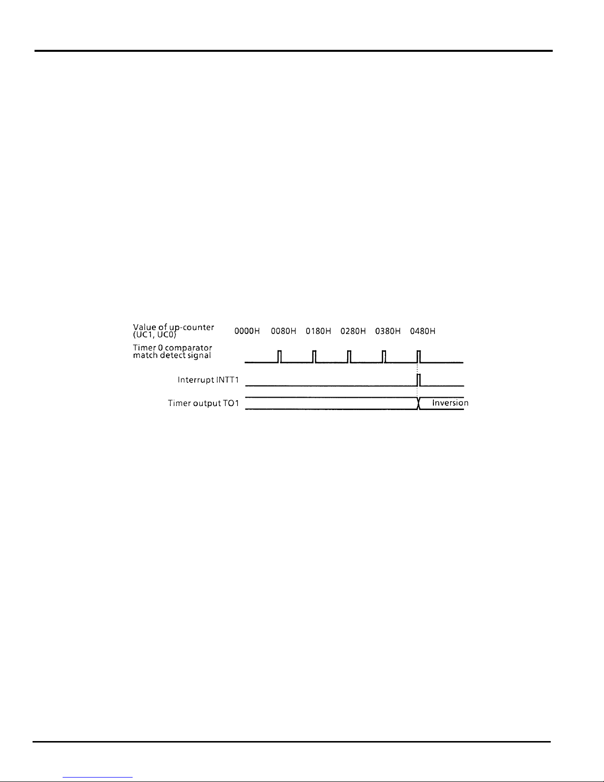
The comparator match signal is output from timer 0
each time the up-counter UC0 matches TREG0, where
the up-counter UC0 is not to be cleared.
With the timer 1 comparator, the match detect signal is
output at each comparator timing when up-counter
UC1 and TREG1 values match. When the match
detect signal is output simultaneously from both comparators of timer 0 and timer 1, the up-counters UC0
and UC1 are cleared to “0”, and the interrupt INTT1 is
generated. If inversion is enabled, the value of the timer
flip-flop TFF1 is inverted.
Example: When TREG1 = 04H and TREG0 = 80H
Figure 3.7 (9). Output Timer by 16-Bit Timer Mode
(3) 8-bit PPG (Programmable Pulse Generation) Output
mode
counter (UC0) matches the timer registers TREG0 and
TREG1.
However, it is required that the set value of TREG0 is
Square wave pulse can be generated at any frequency
and duty by timer 0 and timer 1. The output pulse may
be either low-active or high-active. In this mode, timer
1 cannot be used.
Timer 0 outputs pulse to TO1 pin (also used as P70).
smaller than that of TREG1.
Though the up-counter (UC1) of timer 1 is not used in
this mode, UC1 should be set for counting by setting
TRUN <T1RUN> to 1.
Figure 3.7 (11) shows the block diagram for this mode.
In this mode, a programmable square wave is generated by inverting timer output each time the 8-bit up-
64 TOSHIBA CORPORATION
Page 65
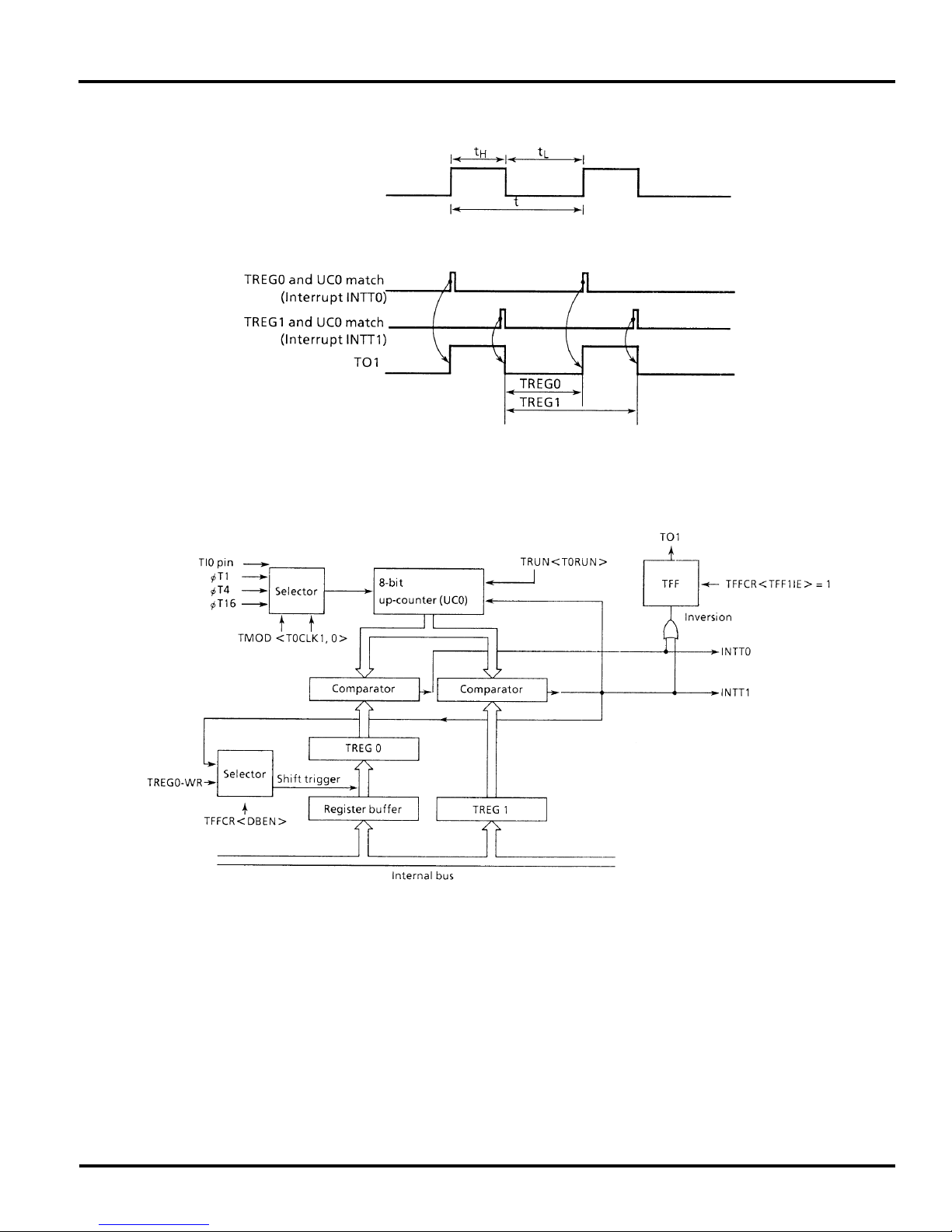
Figure 3.7 (10). 8-Bit PPG Output Waveforms
TMP96C141AF
Figure 3.7 (11). Block Diagram of 8-Bit PPG Output Mode
TOSHIBA CORPORATION 65
Page 66
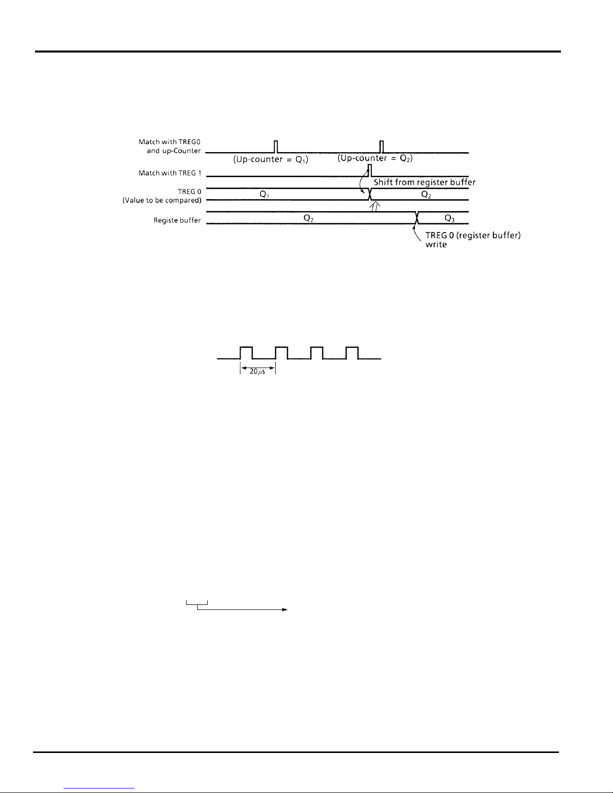
TMP96C141AF
When the double buffer of TREG0 is enabled in this
mode, the value of register buffer will be shifted in TREG0 each
time TREG1 matches UC0.
Figure 3.7 (12). Operation of Register Buffer
Example: Generating 1/4 duty 50KHz pulse @ fc = 16MHz)
Use of the double buffer makes easy handling of low duty
waves (when duty is varied).
• Calculate the value to be set for timer register.
To obtain the frequency 50KHz, the pulse cycle t
should be: t = 1/50KHz = 20µs.
Given φ T1 = 0.5µs @ 16MHz),
20µs ÷ 0.5µs = 40
TREG1 = 40 = 28H and then duty to 1/4, t x 1/4 =
20µs x 1/4 = 5µs
5µs ÷ 0.5µs = 10
Therefore, set timer register 0 (TREG0) to TREG0 = 10
= 0AH.
Consequently, to set the timer register 1 (TREG1) to
76543210
TRUN ← –x––––00 Stop timer 0, and clear it to “0”.
φ
TMOD ← 10xxxx01 Set the 8-bit PPG mode, and select
TREG0 ← 00001010 Write “0AH”.
TREG1 ← 00101000 Write “28H”.
TFFCR ← –––1011x Sets TFF1 and enables the inversion and double buffer enable.
Writing “10” provides negative logic pulse.
P7CR ← xxxx––1–
P7FC ← xxxx––1x
TRUN ← 1x––––11 Start timer 0 and timer 1 counting.
Note : x; don’t care –; no change
Set P71 as TO1 pin.
)
T1 as input clock.
66 TOSHIBA CORPORATION
Page 67
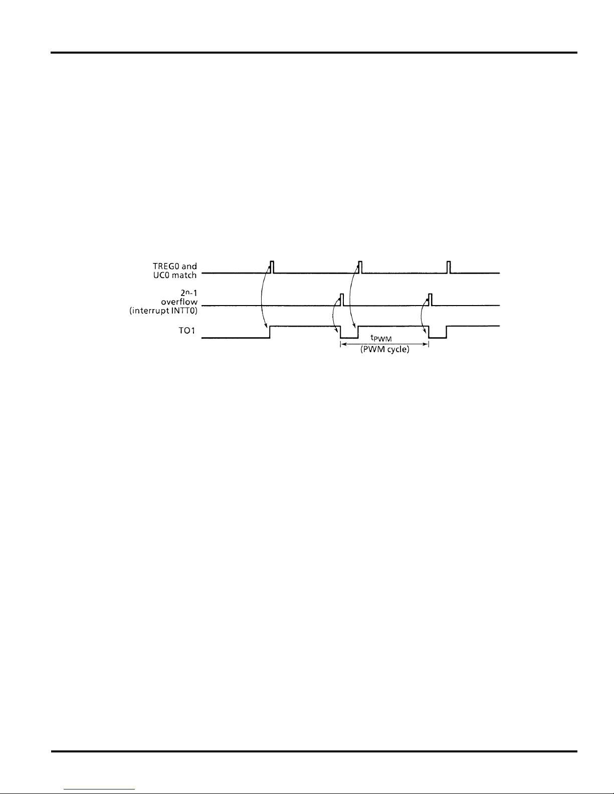
TMP96C141AF
(4) 8-bit PWM Output mode
This mode is valid only for timer 0. In this mode, maximum 8-bit resolution of PWM pulse can be output.
PWM pulse is output to TO1 pin (also used as P71)
when using timer 0. Timer 1 can also be used as 8-bit
timer.
Timer output is inverted when up-counter (UC0)
matches the set value of timer register TREG0 or when
2n - 1 (n = 6, 7, or 8; specified by T01MOD <PWM01,
0>) counter overflow occurs. Up-counter UC0 is
cleared when 2n - 1 counter overflow occurs. For
example, when n = 6, 6-bit PWM will be output, while
when n = 7, 7-bit PWM will be output.
To use this PWM mode, the following conditions must
be satisfied.
(Set value of timer register) <(Set value of 2n - 1
counter overflow)
(Set value of timer register ≠ 0)
Figure 3.7 (13). 8-Bit PWM Waveforms
TOSHIBA CORPORATION 67
Page 68
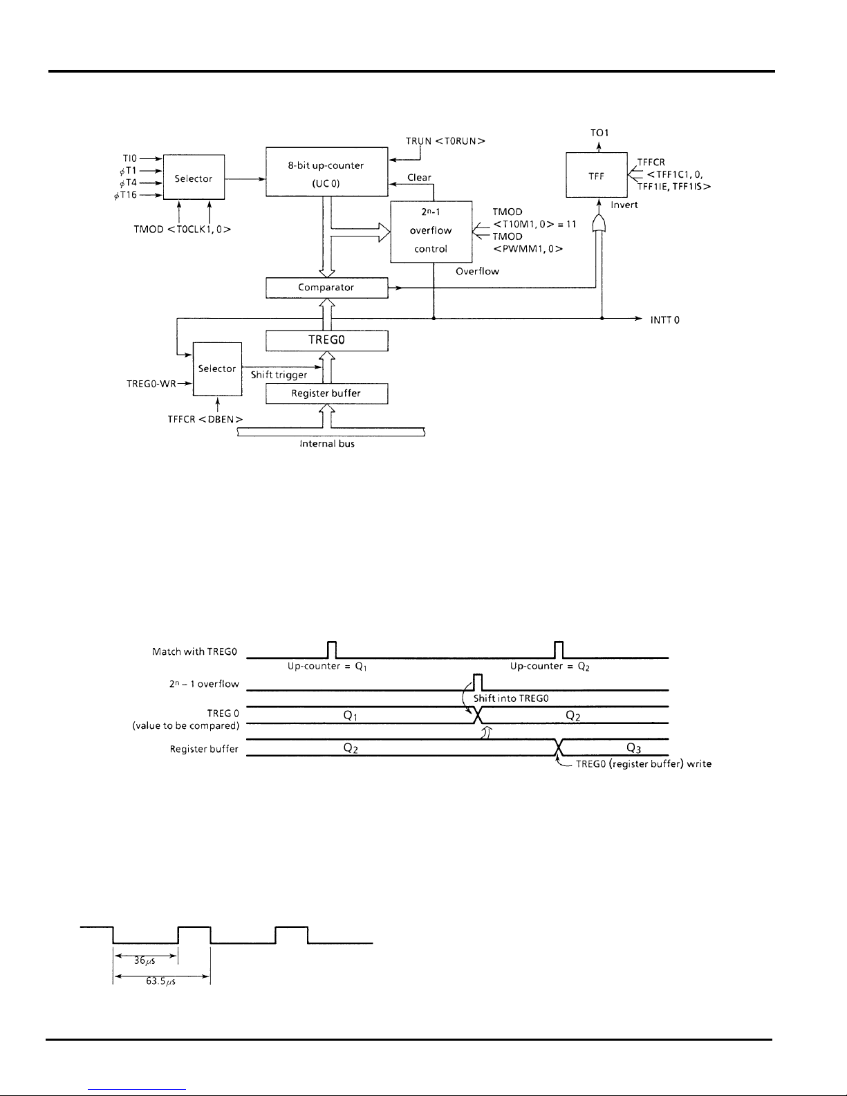
TMP96C141AF
Figure 3.7 (14) shows the block diagram of this mode.
Figure 3.7 (14). Block Diagram of 8-Bit PWM Mode
In this mode, the value of register buffer will be shifted in
TREG0 if 2n - 1 overflow is detected when the double buffer of
waves easy.
TREG0 is enabled.
Figure 3.7 (15). Operation of Register Buffer
Example: To output the following PWM waves to TO1 pin at fc = 16MHz.
16MHz),
Use of the double buffer makes the handling of small duty
To realize 63.5µs of PWM cycle by φT1 = 0.5µs (@ fc =
63.5µs ÷ 0.5µs = 127 = 27 - 1
68 TOSHIBA CORPORATION
Consequently, n should be set to 7.
As the period of low level is 36µs, for φT1 = 0.5µs, set the
following value for TREG0:
36µs ÷ 0.5µs = 72 = 48H
Page 69
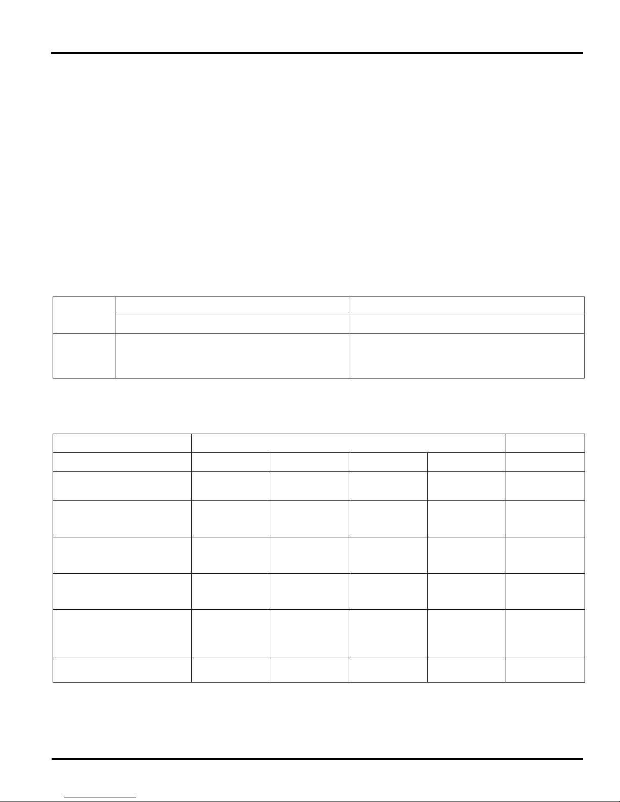
MSB LSB
76543210
TRUN ← - x–––––0 Stop timer 0, and clear it to “0”.
7
TMOD ← 1110––01 Set 8-bit PWM mode (cycle: 2
TREG0 ← 01001000 Write “48H”.
TFFCR ← xxxx101x Clears TFF1, enables the inversion and double buffer.
- 1) and select φT1 as the input clock.
TMP96C141AF
P7CR ← xxxx––1–
P7FC ← xxxx––1x
TRUN ← 1x–––––1 Start timer 0 counting.
Note: x; don’t care –; no change
Set P71 as the TO1 pin.
)
Table 3.7 (3) PWM Cycle and the Setting of 2n -1 Counter
PWM Cycle (@ fc =16MHz) PWM Cycle (@ fc = 20 MHz)
φ
T1
6
-1 31.5µsec (31.7kHz) 126msec (7.9kHz) 0.50µsec (1.9kHz) 25.2µsec (39.0kHz) 100µsec (10.0kHz) 0.40msec (2.4kHz)
2
7
-1 63.5µsec (15.7kHz) 254msec (3.9kHz) 1.01µsec (0.98kHz) 50.8µsec (19.7kHz) 203µsec (4.9kHz) 0.81msec (1.2kHz)
2
8
-1 127µsec (7.8kHz) 510msec (1.9kHz) 2.04µsec (0.49kHz) 102µsec (9.80kHz) 408µsec (2.4kHz) 1.63msec (0.61kHz)
2
φ
T4
φ
T16
(5) Table 3.7 (4) shows the list of 8-bit timer modes.
Table 3.7 (4) Timer Mode Setting Registers
Register Name TMOD TFFCR
Name of Function in T10M PWMM T1CLK T0CLK TFF1IS
Function Timer Mode PWM0 Cycle
16-bit timer mode 01 – –
Lower timer match :
φ
8-bit timer x 2 channels 00 –
8-bit PPG x 1 channel 10 – –
6
2
8-bit PWM x 1 channel 11
- 1, 27 - 1, 28 - 1
(01, 10, 11)
T1, φT16, φT256
(00, 01, 10, 11)
φ
T1
Upper Timer
Input Clock
–
φ
T4
Lower Timer
Input Clock
External clock,
φ
T1, φT4, φT16
(00, 01, 10, 11)
External clock,
φ
T1, φT4, φT16
(00, 01, 10, 11)
External clock,
φ
T1, φT4, φT16
(00, 01, 10, 11)
External clock,
φ
T1, φT4, φT16
(00, 01, 10, 11)
φ
T16
Timer F/F Invert
Signal Select
–
0 : Lower timer output
1 : Upper timer output
–
–
8-bit timer x 1 channel 11 –
Note: –: don’t care
TOSHIBA CORPORATION 69
φ
T1, φT16, φT256
(01, 10, 11)
– Output disabled
Page 70

TMP96C141AF
3.8 8-Bit PWM Timer
The TMP96C141AF/TMP96CM40F/TMP96PM40F has two
built-in 8-bit PWM timers (timers 2 and 3).
They have two operating modes.
• 8-bit PWM (pulse width modulation: variable duty at fixed
interval) output mode
• 8-bit interval timer mode
Figure 3.8 (1) is a block diagram of 8-bit PWM timer (tim-
ers 2 and 3).
PWM timers consist of an 8-bit up-counter, 8-bit comparator, and 8-bit timer register. Two timer flip-flops (TFF2 for
timer 2 and TFF3 for timer 3) are provided.
Input clocks φP1, φP4, and φP16 for the PWM timers can
be obtained using the built-in prescaler.
PWM timer operating mode and timer flip-flops are controlled by four control registers (P0MOD, P1MOD, PFFCR, and
TRUN).
70 TOSHIBA CORPORATION
Page 71
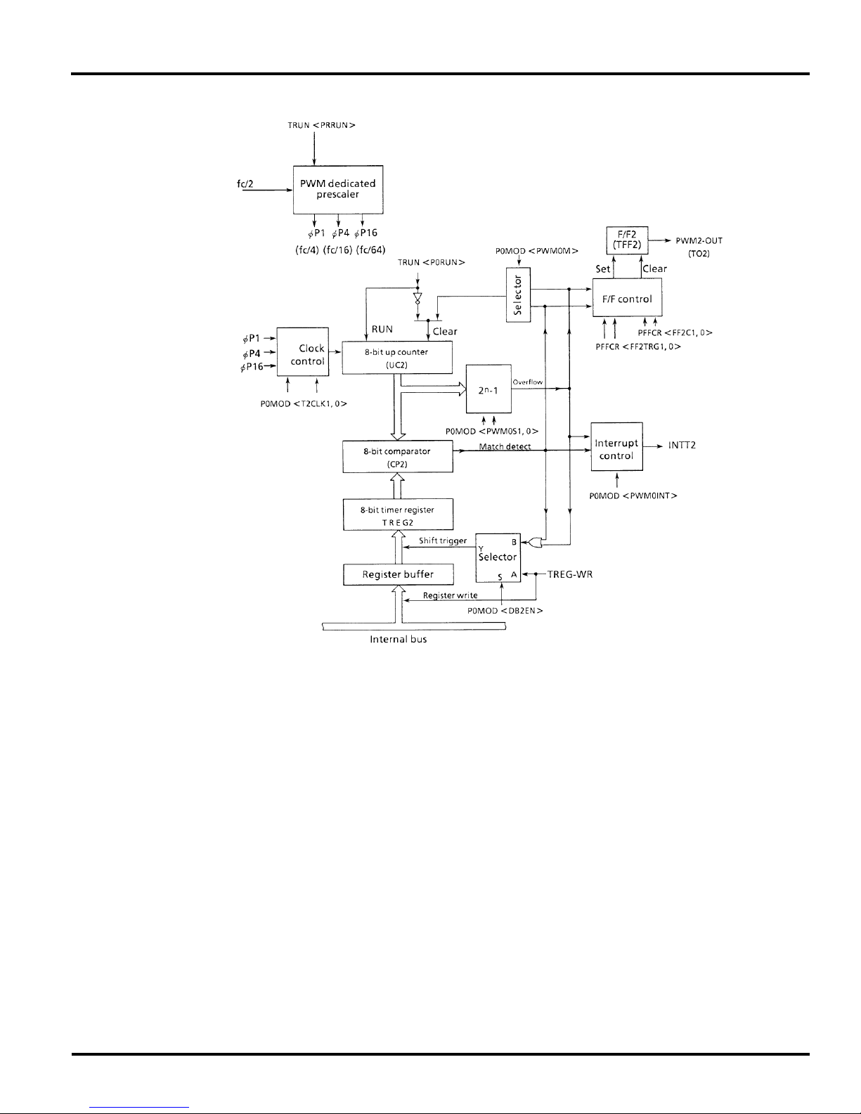
TMP96C141AF
Figure 3.8 (1). Block Diagram of 8-Bit PWM Timer 0 (Timer 2)
Note: Block diagram for 8-bit PWM timer 1 (timer 3) is the same as the above diagram.
TOSHIBA CORPORATION 71
Page 72
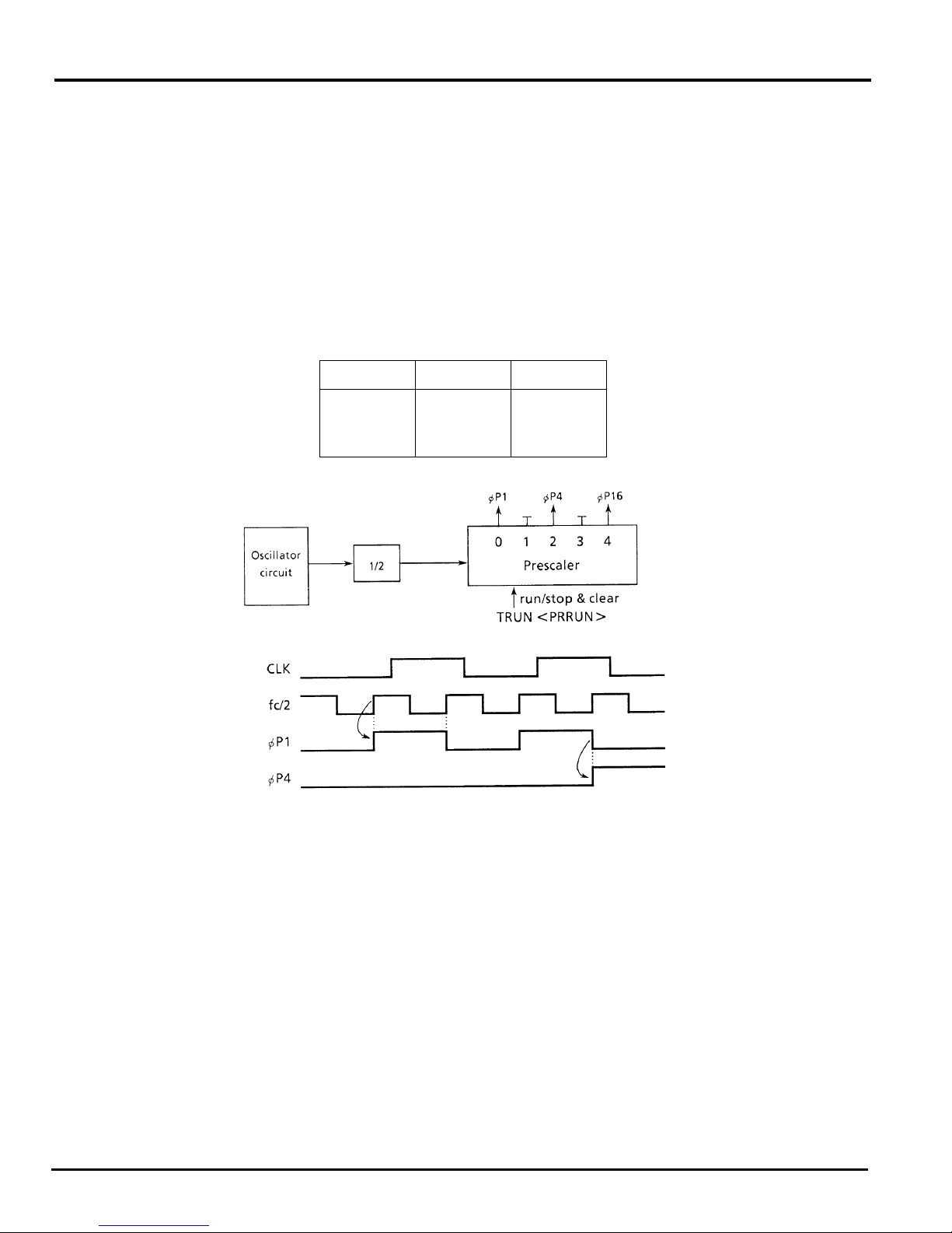
TMP96C141AF
➀ Prescaler
Generates input clocks dedicated to PWM timers by
further dividing the fundamental clock (fc) after it has
been divided by 2 (fc/2). Since the register used to
control the prescaler is the same as the one for other
timers, the prescaler cannot be operated independently.
Dedicated Prescaler Cycle
φ
P1 (4/fc) 250ns 200ns
φ
P4 (16/fc) 1µs 800ns
φ
P16 (64/fc) 4µs 3.2µsc
The PWM timer uses three input clocks: φ/P1, φ/P4,
and φ/P16.
Like the 9-bit prescaler described in the 8-bit timer
section, this prescaler can be counted/stopped using
bit 7 <PRRUN> of the timer operation control register
TRUN. Setting <PRRUN> to 1 starts counting; setting
it to 0 zero-clears and stops counting. Resetting clears
<PRRUN> to 0, which clears and stops the prescaler.
16MHz 20MHz
➁ Up-counter
An 8-bit binary counter which counts up using the
input clock specified by PWM mode register (P0MOD
or P1MOD).
The input clock for the PWM0/PWM1 is selected from
the internal clocks φP1, φP4, and φP16 (PWM dedicated prescaler output) depending on the value set in
the P0MOD/P1MOD register.
Operating mode is also set by P0MOD and P1MOD
registers. At reset, they are initialized to P0MOD
<PWM0M> = 0 and P1MOD <PWM1M> = 0, thus, the
up-counter is in PWM mode. In PWM mode, the upcounter is cleared when a 2n - 1 overflow occurs; in
timer mode, the up-counter is cleared at compare and
72 TOSHIBA CORPORATION
Figure 3.8 (2). Prescaler
match.
Count/stop and clear of the up-counter can be con-
trolled for each PWM timer using the timer operation
control register TRUN. Resetting clears all up-counters
and stops timers.
➂ Timer registers
Two 8-bit registers used for setting an interval time.
When the value set in the timer registers (TREG 2 and
3) matches the value in the up-counter, the match
detect signal of the comparator becomes active.
Timer registers TREG2 and TREG3 are each paired
with register buffer to make a double buffer structure.
Page 73
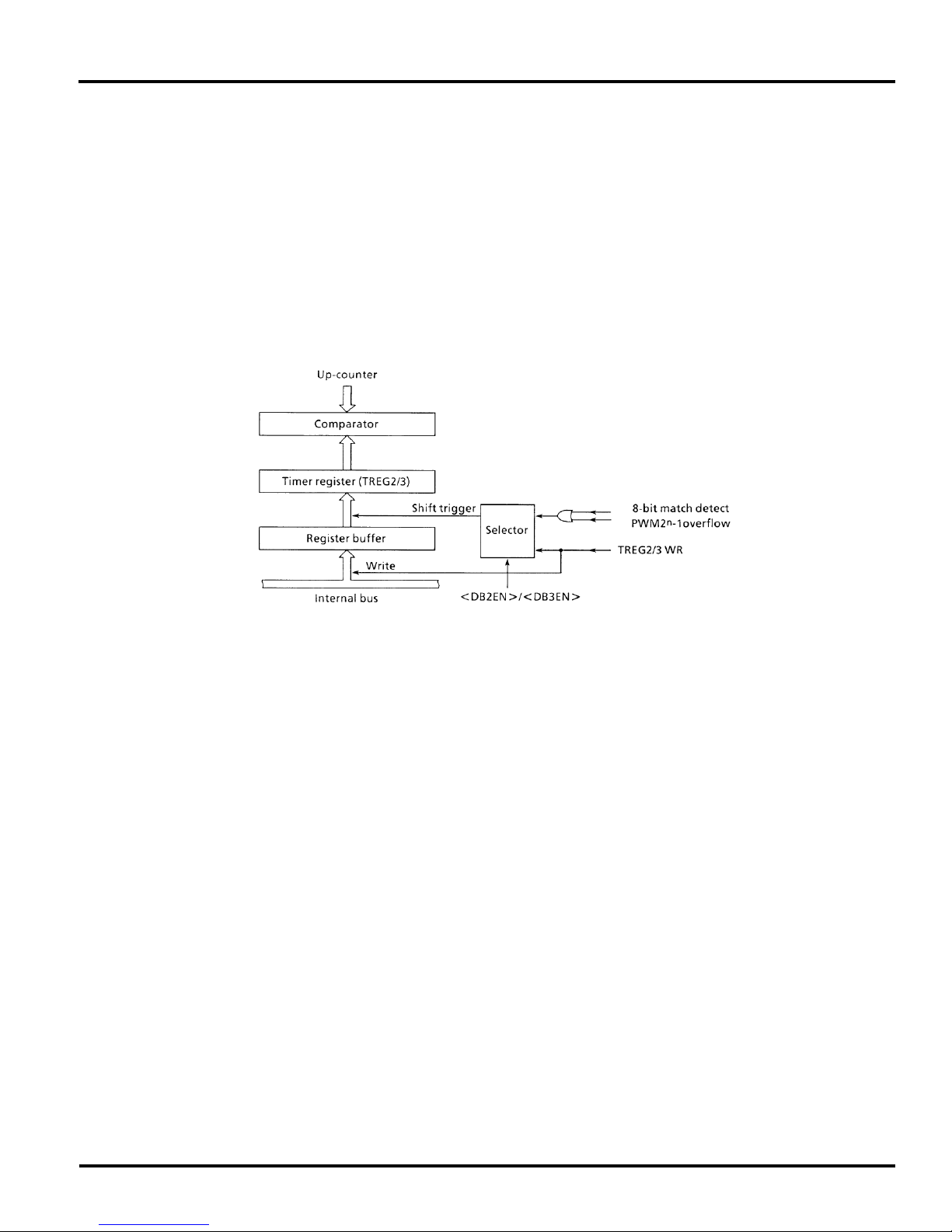
TMP96C141AF
TREG2 and TREG3 are controlled double buffer
enable/disable by P0MOD <DB2EN> and P1MOD
<DB3EN> : disabled when <DB2EN>/<DB3EN> = 0,
enabled when <DB2EN>/<DB3EN> = 1.
Data is transferred from register buffer to timer when a
2n - 1 overflow occurs in the PWM mode, or when
compare and match occurs in 8-bit timer mode. That
is, with a PWM timer, the timer mode can be operated
in double buffer enable state, unlike timer mode for
timers 0 and 1.
At reset, <DB2EN>/<DB3EN> is initialized to 0 to disable double buffer. To use double buffer, write the data
in the timer register at first, then set <DB2EN>/
<DB3EN> to 1, and write the following data in the register buffer.
Figure 3.8 (3). Structure of Timer Registers 2 and 3
Note: The timer register and register buffer are allocated to the same
memory address. When <DB2EN>/<DB3EN> = 0, the same value
is written to both register buffer and timer register. When <DB2EN>/
<DB3EN> = 1, the value is written to the register buffer only.
Memory addresses of the timer registers are as follows:
TREG2 : 000026H
TREG3 : 000027H
Both timer registers are write only; however, register
buffer values can be read when reading the above
addresses.
➃ Comparator
Compares the value in the up-counter with the value in
the timer register (TREG2/TREG3). When they match,
the comparator outputs the match detect signal. A
timer interrupt (INTT2/INTT3) is generated at compare
and match if the interrupt select bit <PWM01NT>/
<PWM1NT> of the mode register (P0MOD/P1MOD) is
set to 1. In timer mode, the comparator clears the upcounter to 0 at compare and match. It also inverts the
value of the timer flip-flop if timer flip-flop invert is
enabled.
➄ Timer flip-flop
The value of the timer flip-flop is inverted by the match
detect signal (comparator output) of each interval timer
or 2n - 1 overflow. The value can be output to the timer
output pin TO2/TO3 (also used as P72/P73).
TOSHIBA CORPORATION 73
Page 74
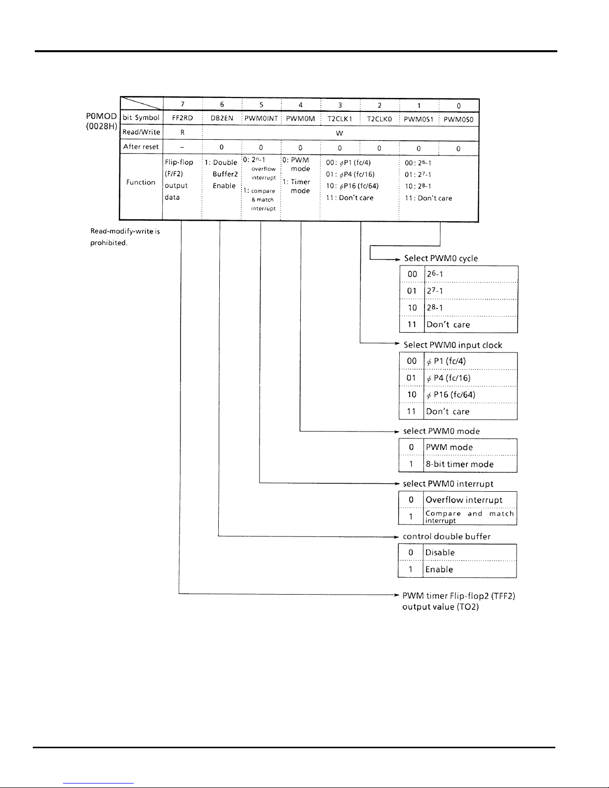
TMP96C141AF
Figure 3.8 (4). 8-Bit PWM0 Mode Control Register
74 TOSHIBA CORPORATION
Page 75
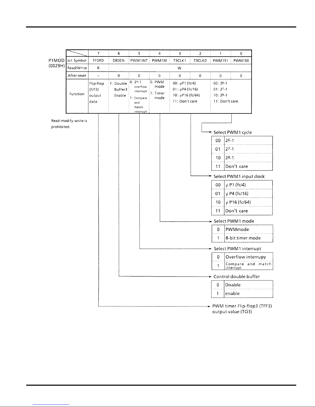
TMP96C141AF
Figure 3.8 (5). 8-Bit PWM1 Mode Control Register
TOSHIBA CORPORATION 75
Page 76
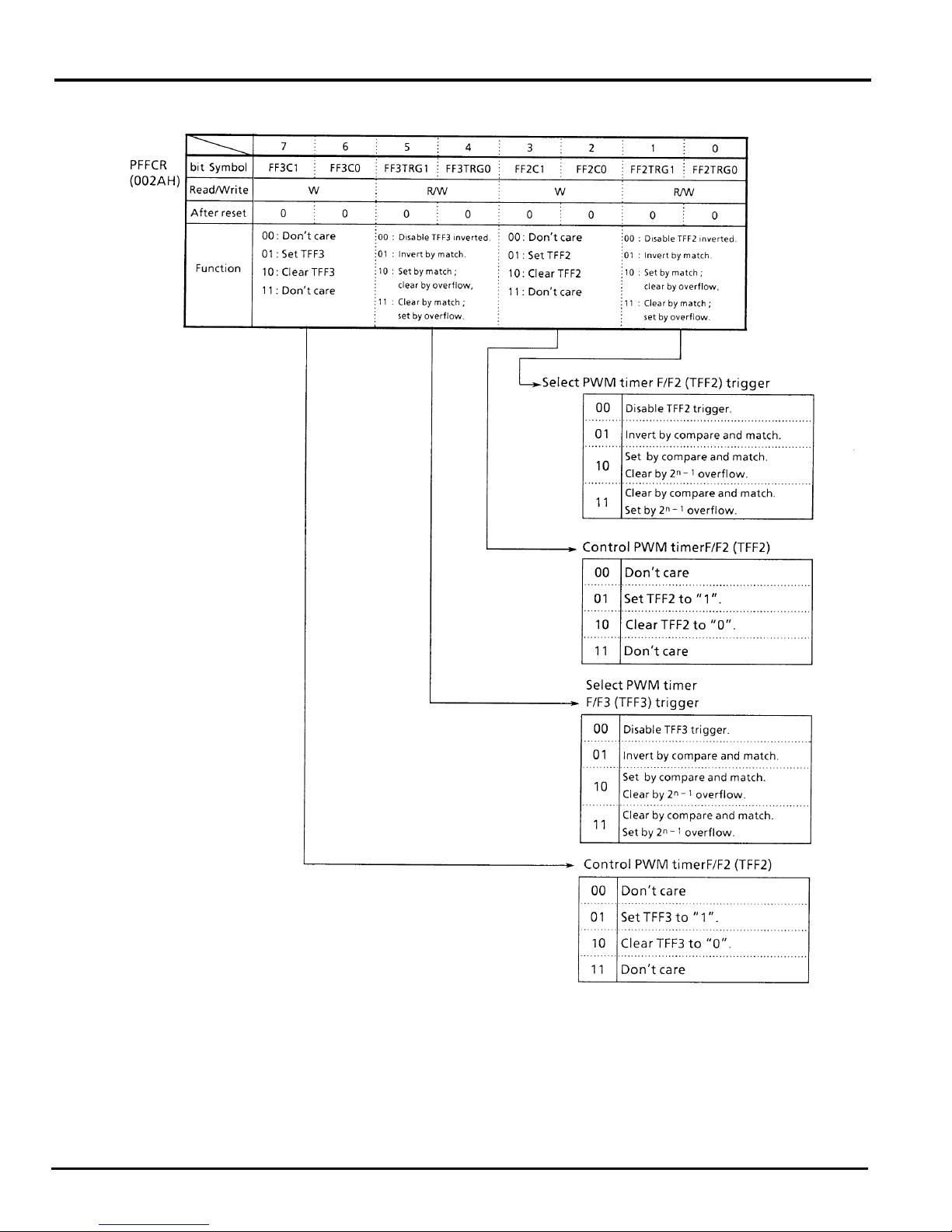
TMP96C141AF
Figure 3.8 (6). 8-Bit PWM F/F Control Register
76 TOSHIBA CORPORATION
Page 77
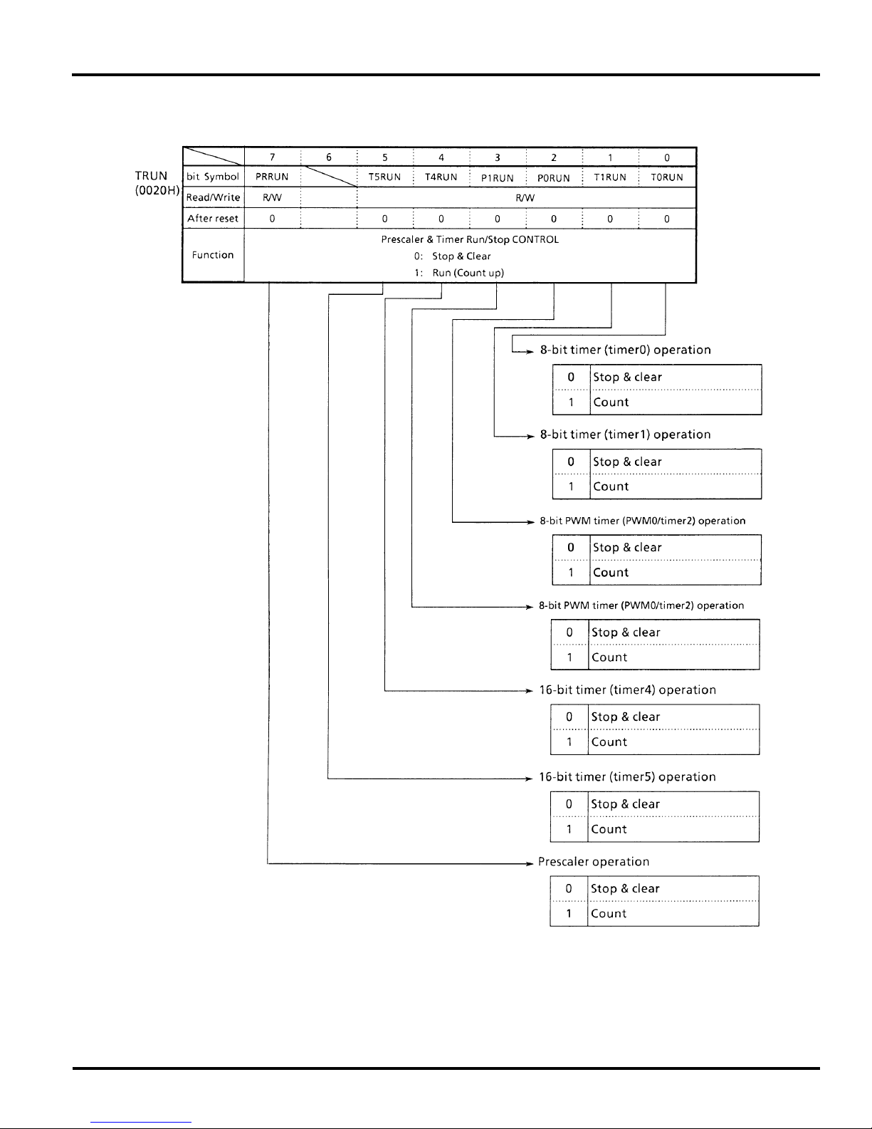
TMP96C141AF
Figure 3.8 (7). Timer Operation Control Register (TRUN)
TOSHIBA CORPORATION 77
Page 78
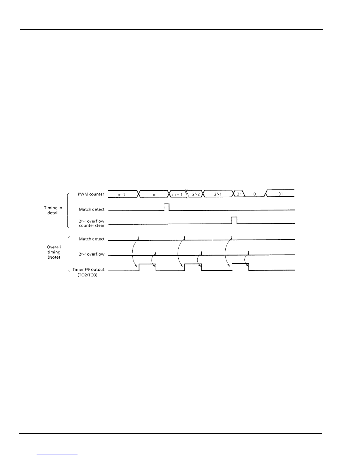
TMP96C141AF
The following explains PWM timer operations.
(1) PWM timer mode
Both PWM timers can output 8-bit resolution PWM
independently. Since both timers operate in exactly the
same way, PWM0 is used for purposes of explanation.
PWM output changes under the following two conditions.
Condition 1:
• TFF2 is cleared to 0 when the value in the upcounter (UC2) and the value set in the TREG2
match.
• TFF2 is set to 1 when a 2n - 1 counter overflow (n
= 6, 7, or 8) occurs.
PWM timing
Condition 2:
• TFF2 is set to 1 when the value in the up-counter
(UC2) and the value set in TREG2 match.
• TFF2 is cleared to 0 when a 2n - 1 counter over
flow (n = 6, 7, or 8) occurs.
The up-counter (UC2) is cleared by a 2n - 1 counter
overflow.
The PWM timer can output 0% - 100% duty pulses
because a 2n - 1 counter overflow has a higher priority.
That is, to obtain 0% output (always low), the mode
used to set TFF2 to 0 due to overflow (PFFCR
<FF2TRG1, 0> = 1, 0) must be set and 2
n
- 1 (value for
overflow) must be set in TREG2. To obtain 100% output (always high), the mode must be changed: PFFCR
<FF2TRG1, 0> = 1,1 then the same operation is
required.
Figure 3.8 (8). Output Waves in PWM Timer Mode
Note: The above waves are obtained in a mode where the F/F is set by a match with the timer register (TREG) and reset by an overflow.
78 TOSHIBA CORPORATION
Page 79
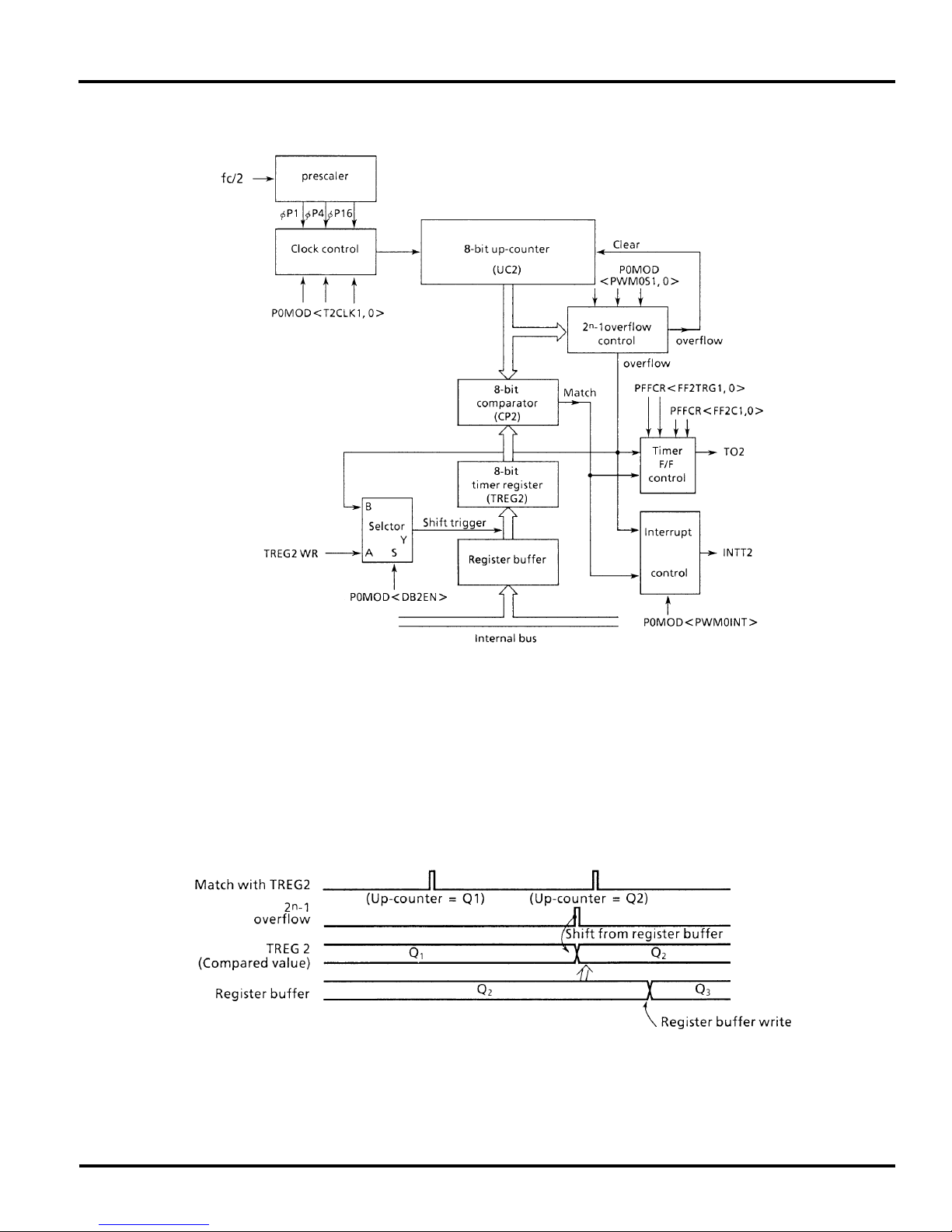
Figure 3.8 (9) is a block diagram of this mode.
TMP96C141AF
Figure 3.8 (9). Block Diagram of PWM Timer Mode (PWM0)
In this mode, enabling double buffer is very useful. The
register buffer value shifts into TREG2 when a 2n -1 overflow
is detected, when double buffer is enabled.
Figure 3.8 (10). Register Buffer Operation
Using double buffer makes handling small duty waves
easy.
TOSHIBA CORPORATION 79
Page 80
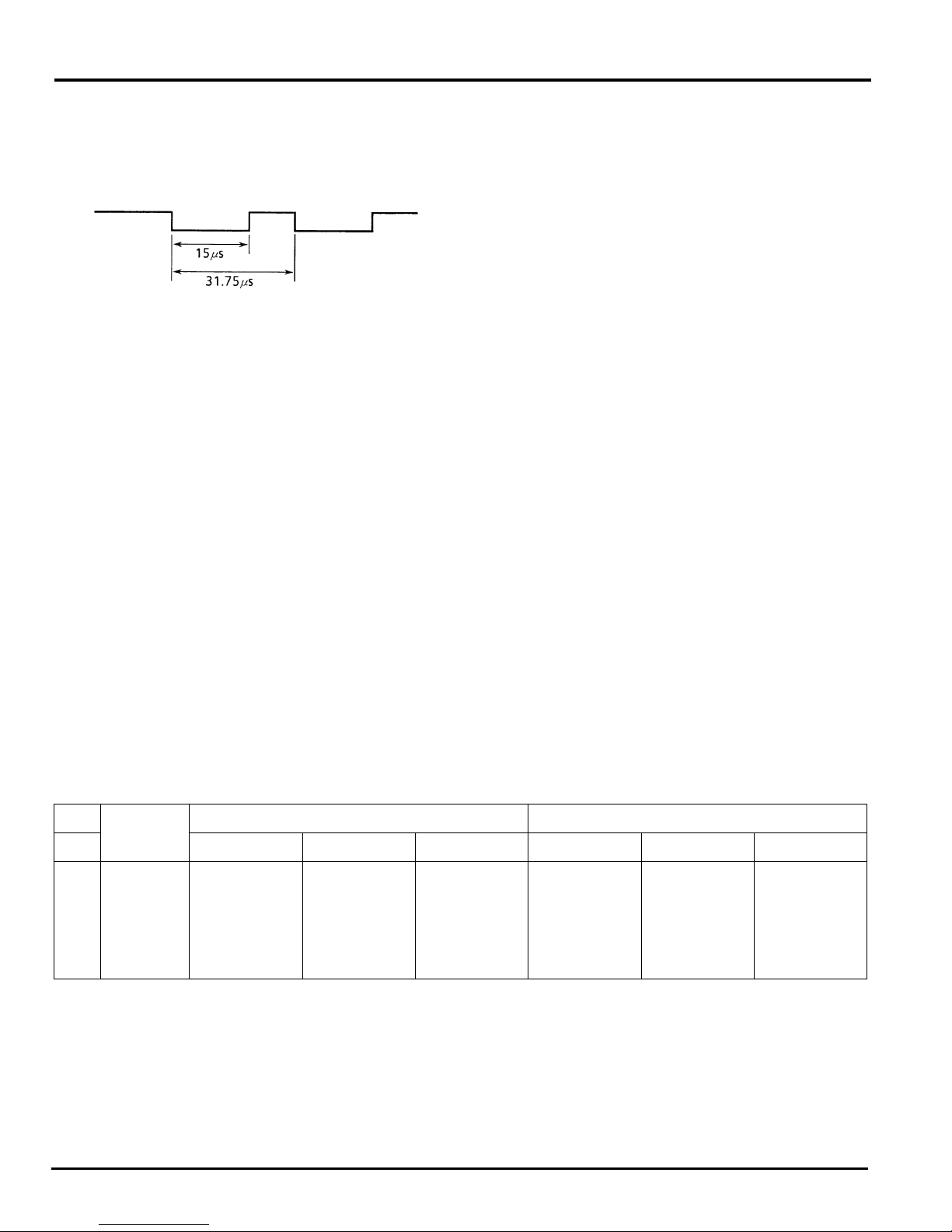
TMP96C141AF
Example: To output the following PWM waves to TO2 pin using PWM0 at fc = 16MHz.
To implement 31.75µs PWM cycle by φ P1 = 0.25µs (@ fc
= 16MHz)
31.75µs ÷ 0.25µs = 127 = 27 -1.
Consequently, set n to 7.
Since the low level cycle = 15µs; for φ P1 = 0.25µs
15µs ÷ 0.25 = 60 = 3CH
set the 3CH in TREG2.
76543210
TRUN ← –x–––0–– Stops PWM0 and clears it to 0.
7
P0MOD ← - 0000001 Sets PWM (2
- 1) mode, input clock φP1, overflow interrupt, and disables double buffer.
TREG2 ← 00111100 Writes 3CH.
P0MOD ← –1000001 Enables double buffer.
PFFCR ← ––––0111 Sets TFF2 and a mode where TFF2 is set by compare and match, and cleared by overflow.
P7CR ← xxxx–1––
P7FC ← xxxx–1–x
TRUN ← 1x–––1–– Starts PWM0 counting.
Note: x; don’t care –; no change
Sets P72 as the TO2 pin.
)
Table 3.8 (1) PWM Cycle and 2n -1 Counter Setting
Formula
φ
6
-1 26-1 - φPn 15.8µsec
2
(63kHz)
7
-1 27-1 - φPn 31.8µsec
2
(31kHz)
8
-1 28-1 - φPn 63.8µsec
2
(16kHz)
P1
16MHz 20MHz
φ
P4
63.0µsec
(16kHz)
127.0µsec
(7.9kHz)
255.0µsec
(3.9kHz)
φ
P16
252µsec
(3.9kHz)
508µsec
(1.9kHz)
1020µsec
(0.98kHz)
φ
P1
12.6µsec
(79kHz)
25.4µsec
(39kHz)
51.0µsec
(20kHz)
φ
P4
50.4µsec
(20kHz)
101.6µsec
(9.8kHz)
204.0µsec
(4.9kHz)
φ
P16
201µsec
(4.9kHz)
406µsec
(2.5kHz)
816µsec
(1.2kHz)
80 TOSHIBA CORPORATION
Page 81
TMP96C141AF
(2) 8-bit timer mode
Both PWM timers can be used independently as 8-bit
interval timers. Since both timers operate in exactly the
same way, PWM0 (timer 2) is used for the purposes of
explanation.
➀ Generating interrupts at a fixed interval
To generate timer 2 interrupt (INTT2) at a fixed interval
using PWM0 timer, first stop PWM0, then set the operating mode, input clock, and interval in the P0MOD
and TREG2 registers. Next, enable INTT2 and start
counting PWM0.
Example: To generate a timer 2 interrupt every 40µs
at fc = 16MHz, set registers as follows:
76543210
TRUN ← –x–––0–– Stops PWM0 and clears it to 0.
φ
P0MOD ← x01100xx Sets 8-bit timer mode and selects
TREG2 ← 10100000 Sets 40µs/0.25µs = A0H in timer register.
INTEPW10 ← ––––1100 Enables INTT2 and sets interrupt level 4.
TRUN ← 1x–––1–– Starts PWM0 counting.
Note: x; don’t care –; no change
P1 (0.25µs) and compare interrupt.
Select an input clock using the table below.
Table 3.8 (2) Interrupt Cycle and Input Clock Selection using 8-Bit Timer Mode
Input Clock
φ
P1 (4/fc) 0.25µs ~ 64µs 0.25µs 0.2µs ~ 51.2µs 0.2µs
φ
P4 (16/fc) 1µs ~ 256µs1µs 0.8µs ~ 204.8µs 0.8µs
φ
P16 (64/fc) 4µs ~ 1024µs4µs 3.2µs ~ 819.2µs 3.2µs
Note: To generate interrupts in 8-bit timer mode, bit 5 (interrupt control bit <PWM01NT>/<PWM1NT> of P0MOD/P1MOD) must be set to 1.
Interrupt Cycle
(at fc = 16MHz)
Resolution
Interrupt Cycle
(at fc = 20MHz)
Resolution
TOSHIBA CORPORATION 81
Page 82
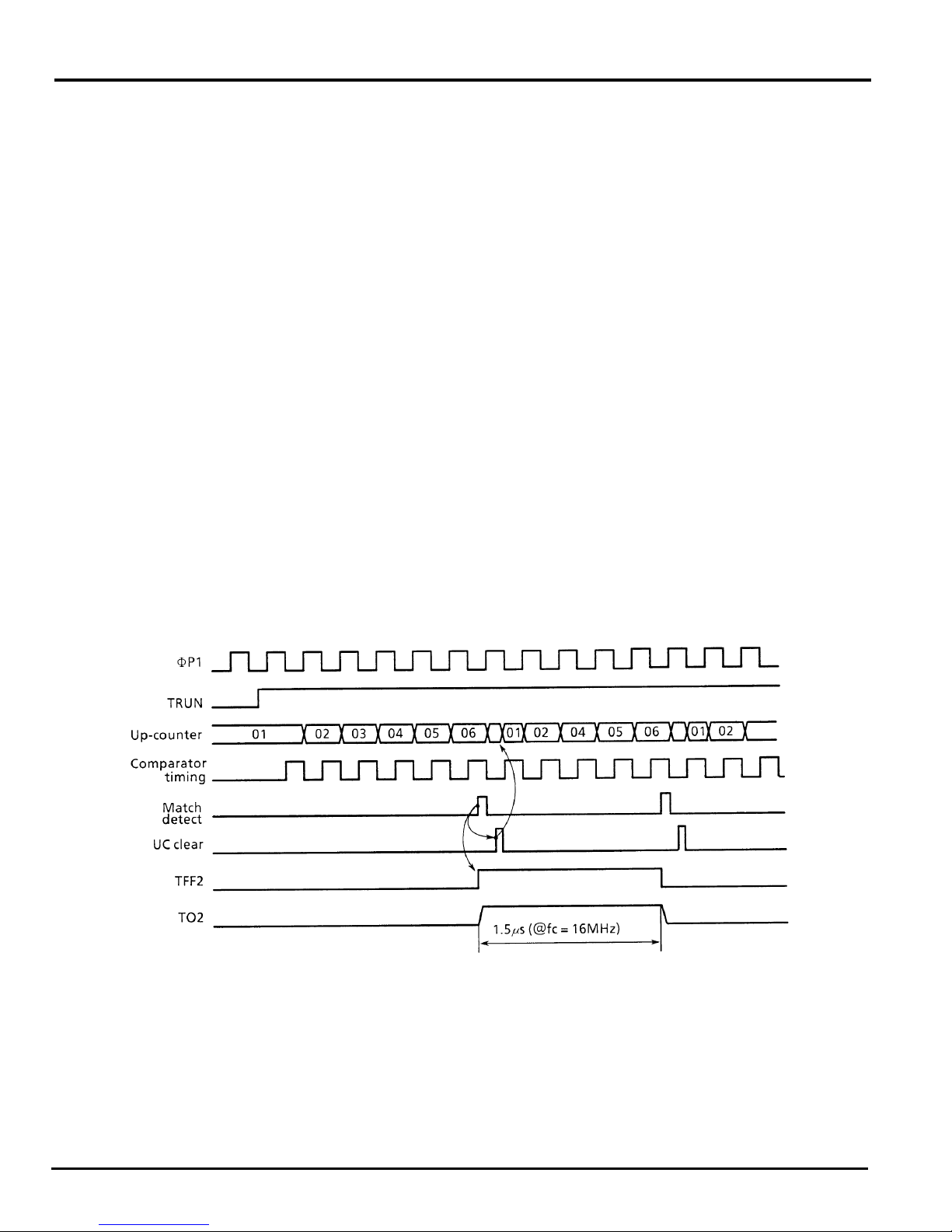
TMP96C141AF
➁ Generating a 50% square wave
To generate a 50% square wave, invert the timer flipflop at a fixed interval and output the timer flip-flop
value to the timer output pin (TO2).
Example: To output a 3.0µs square wave at fc =
16MHz from TO2 pin, set register as fol-
lows:
76543210
TRUN ← –x–––0–– Stops PWM0 and clears it to 0.
φ
P0MOD ← x01100xx Sets 8-bit timer mode and selects
TREG2 ← 00000110 Sets 3.0µs/0.25µs/2 = 6 in the timer register.
PFFCR ← ––––1001 Clears TFF2 to 0 and inverts using comparator output.
P7CR ← xxxx–1––
P7FC ← xxxx–1–x
TRUN ← 1x–––1––
Note: x; don’t care –; no change
Sets P72 as the TO2 pin.
)
P1 (0.25µs) as the input clock.
Figure 3.8 (11). Square Wave (50% Duty) Output Timing Chart
82 TOSHIBA CORPORATION
Page 83
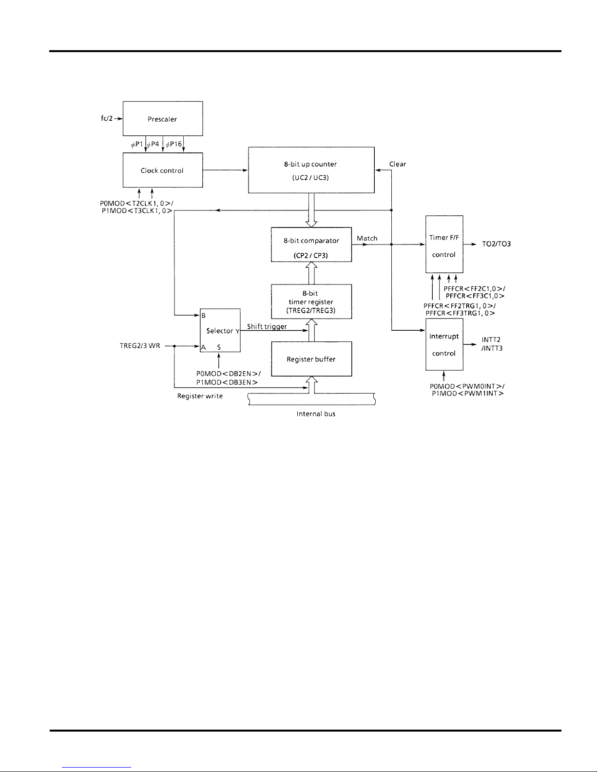
This mode is as shown in Figure 3.8 (12) below.
TMP96C141AF
Figure 3.8 (12). Block Diagram of 8-Bit Timer Mode
TOSHIBA CORPORATION 83
Page 84

TMP96C141AF
3.9 16-Bit Timer
The TMP96C141AF has two (timer 4 and timer 5) multifunctional 16-bit timer/event counter with the following operation
modes.
• 16-bit interval timer mode
• 16-bit event counter mode
• 16-bit programmable pulse generation (PPG) mode
• Frequency measurement mode
• Pulse width measurement mode
• Time differential measurement mode
Timer/event counter consists of 16-bit up-counter, two
16-bit timer registers, two 16-bit capture registers (one of them
applies double-buffer), two comparators, capture input controller, and timer flip-flop and the control circuit.
Timer/event counter is controlled by four control registers: T4MOD/T5MOD, T4FFCR/T5FFCR, TRUN and T45CR.
Figure 3.9 (1) and (2) show the block diagram of 16-bit
timer/event counter (timer 4 and timer 5).
84 TOSHIBA CORPORATION
Page 85
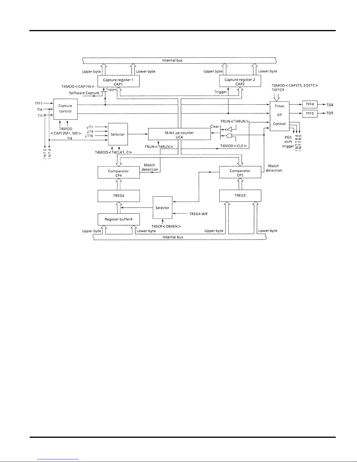
TMP96C141AF
Figure 3.9 (1). Block Diagram of 16-Bit Timer (Timer 4)
TOSHIBA CORPORATION 85
Page 86
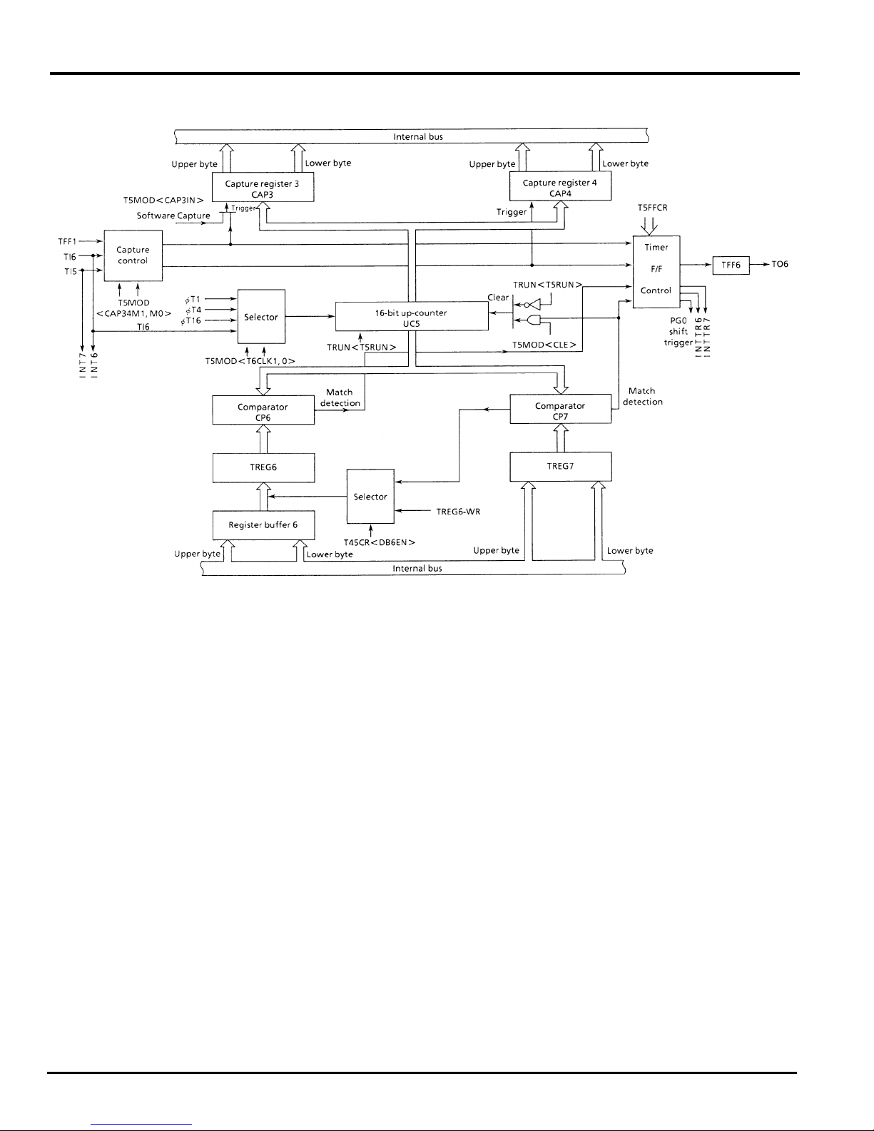
TMP96C141AF
Figure 3.9 (2). Block Diagram of 16-Bit Timer (Timer 5)
86 TOSHIBA CORPORATION
Page 87
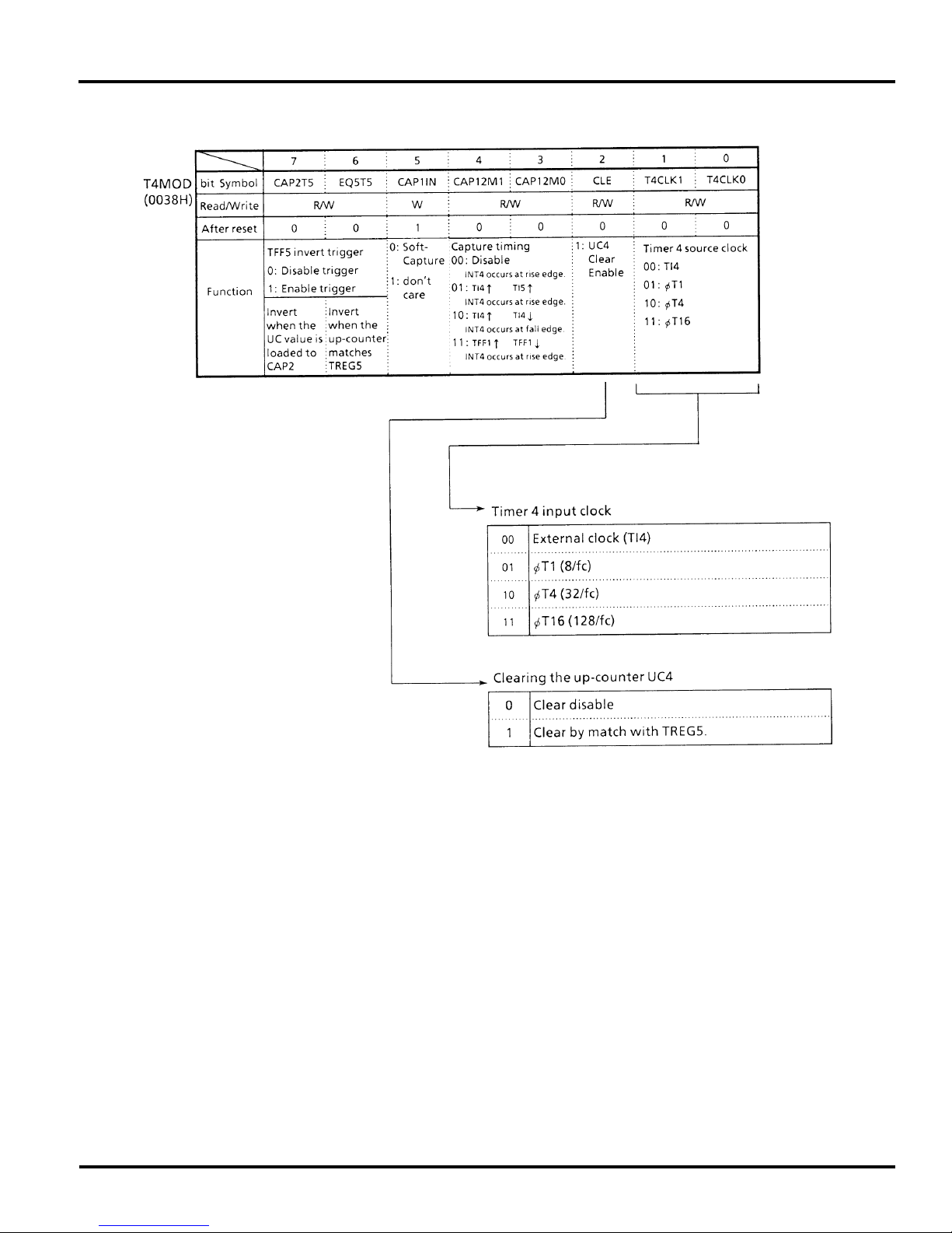
TMP96C141AF
Figure 3.9 (3). 16-Bit Timer Mode Controller Register (T4MOD) (1/2)
TOSHIBA CORPORATION 87
Page 88
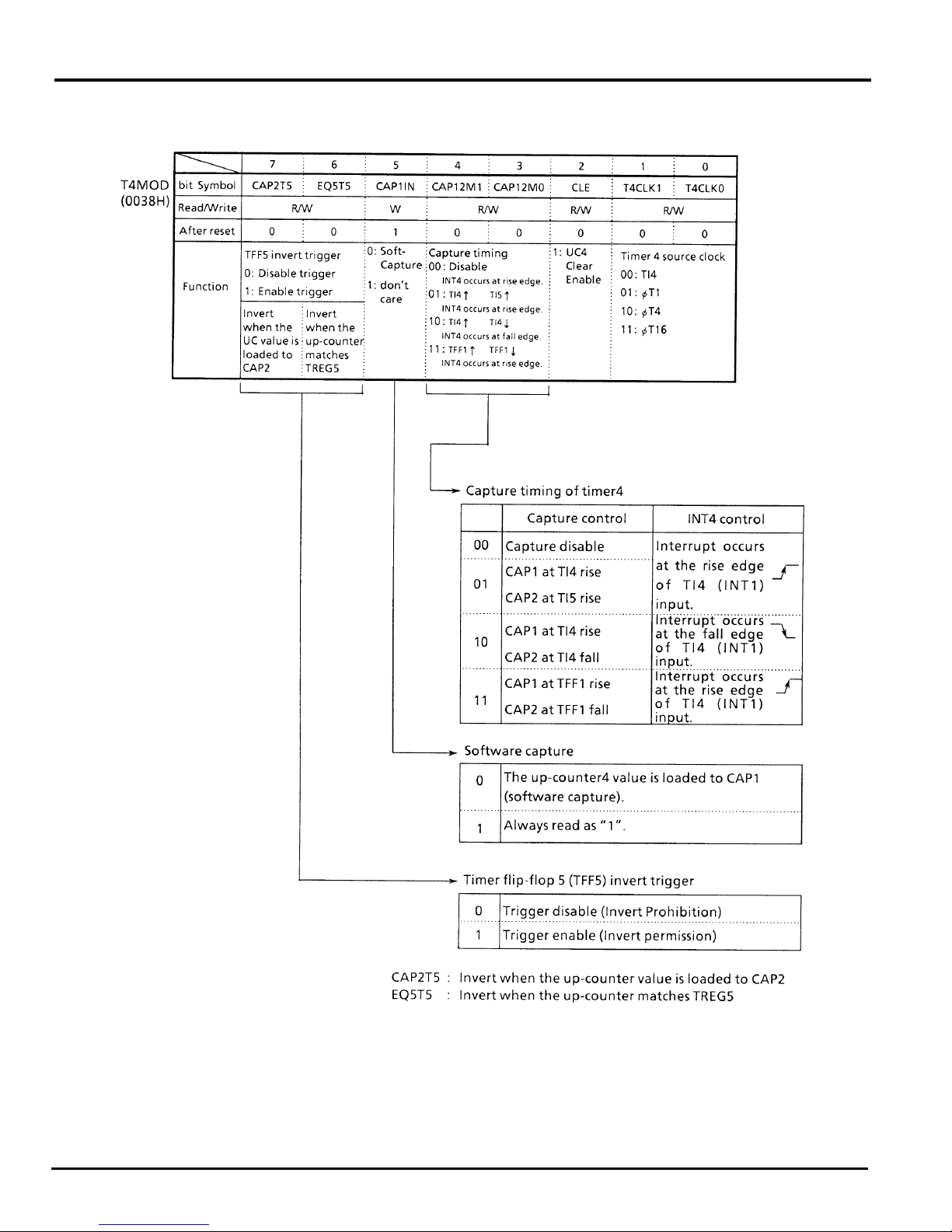
TMP96C141AF
Figure 3.9 (4). 16-Bit Controller Register (T4MOD) (2/2)
88 TOSHIBA CORPORATION
Page 89
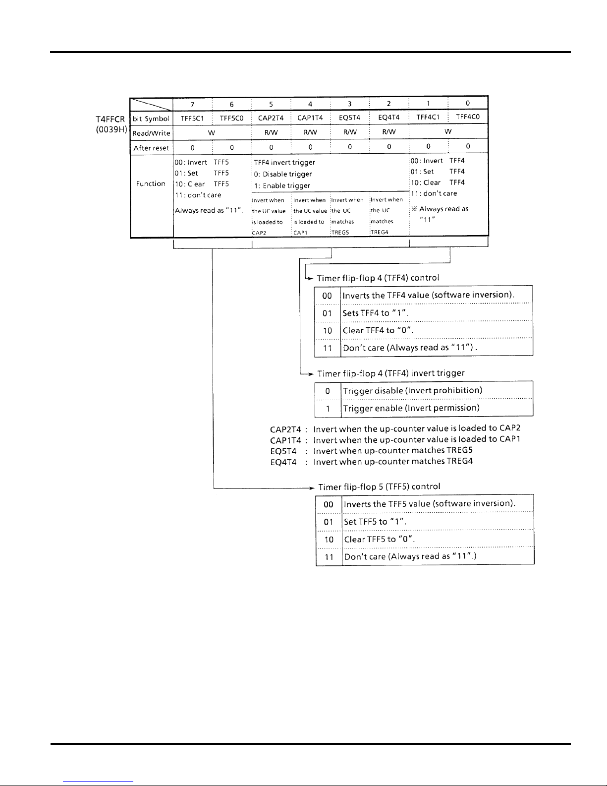
TMP96C141AF
Figure 3.9 (5). 16-Bit Timer 4 F/F Control (T4FFCR)
TOSHIBA CORPORATION 89
Page 90
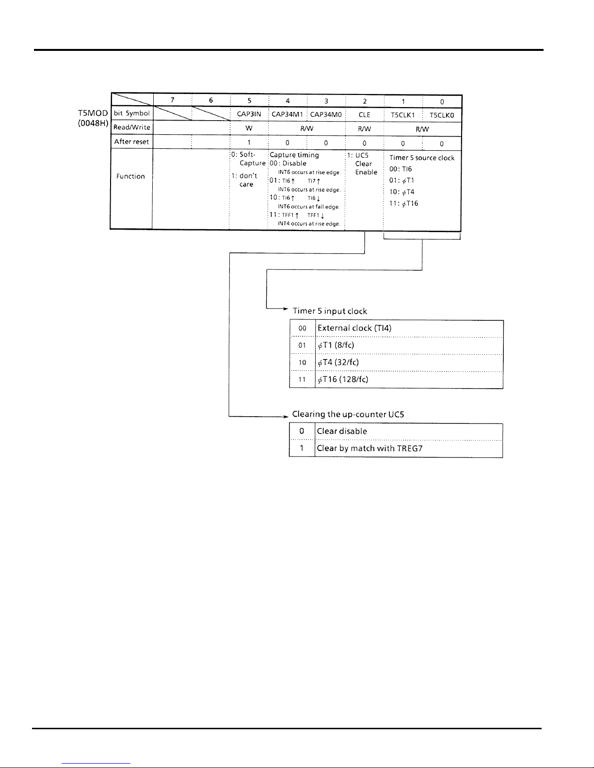
TMP96C141AF
Figure 3.9 (6). 16-Bit Timer Mode Control Register (T5MOD) (1/2)
90 TOSHIBA CORPORATION
Page 91
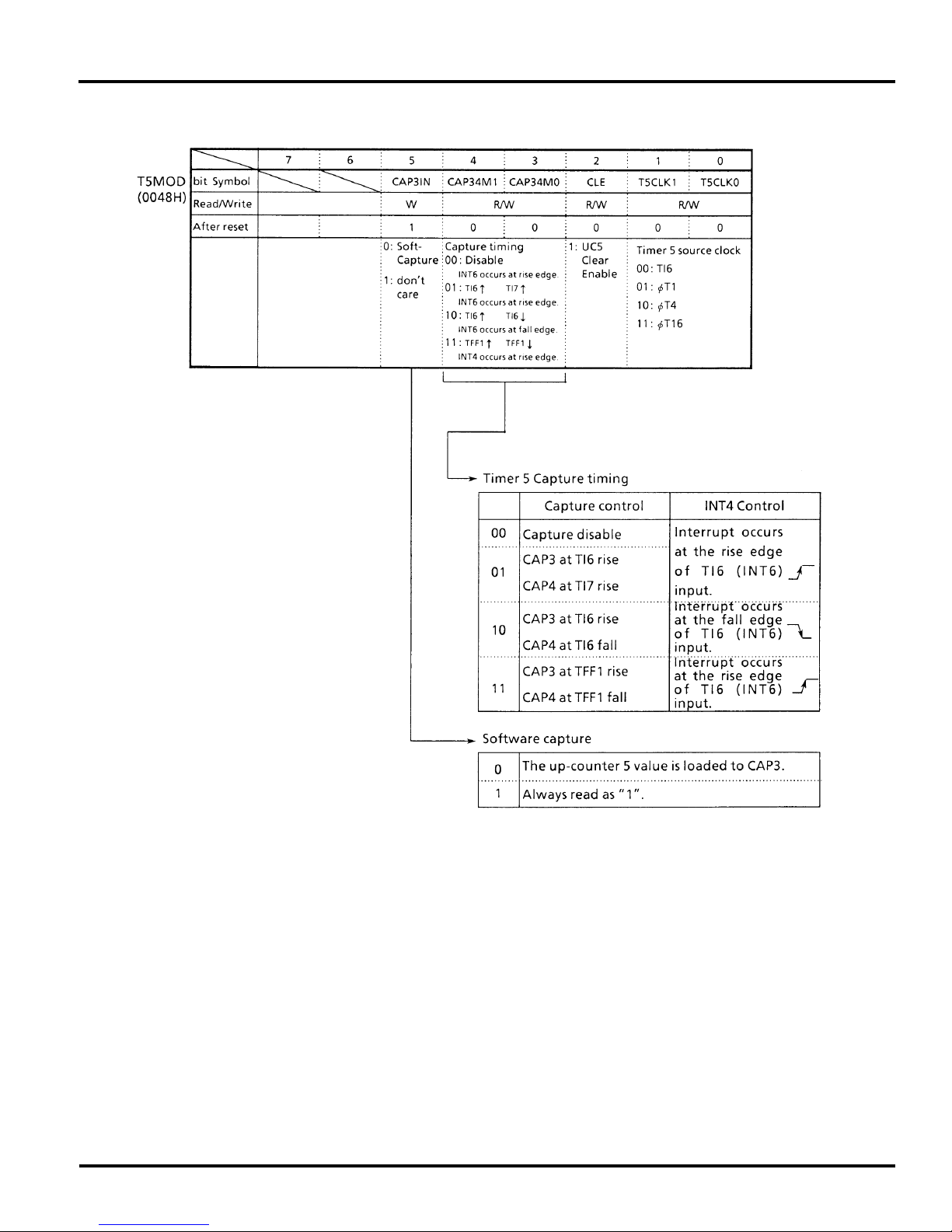
TMP96C141AF
Figure 3.9 (7). 16-Bit Timer Control Register (T5MOD) (2/2)
TOSHIBA CORPORATION 91
Page 92
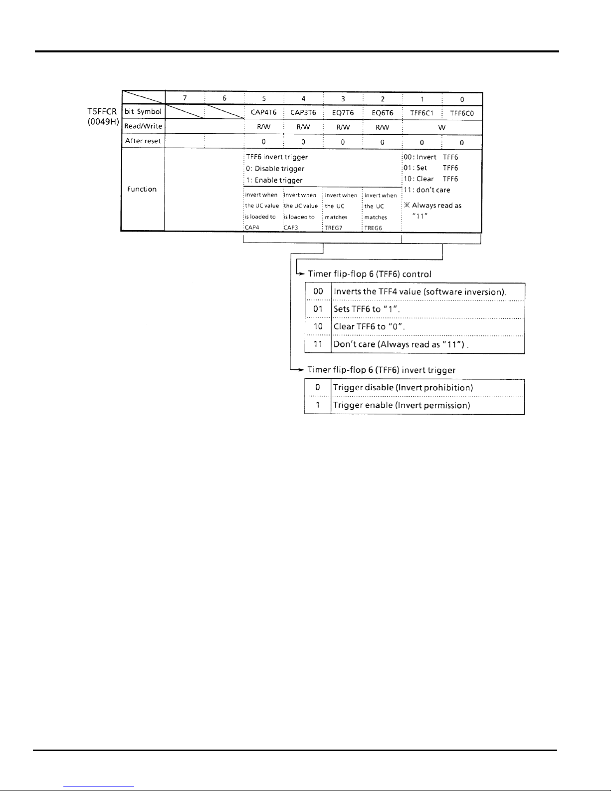
TMP96C141AF
CAP4T6 : Invert when the up-counter value is loaded to CAP4
CAP3T6 : Invert when the up-counter value is loaded to CAP3
EQ7T6 : Invert when up-counter matches TREG7
EQ6T6 : Invert when up-counter matches TREG6
Figure 3.9 (8). 16-Bit Timer 5 F/F Control (T5FFCR)
92 TOSHIBA CORPORATION
Page 93
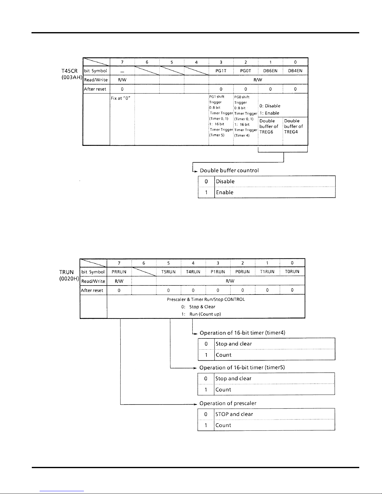
TMP96C141AF
DB6EN : Double buffer of TREG6
DB4EN : Double buffer of TREG4
Figure 3.9 (9). 16-Bit Timer (Timer 4, 5) Control Register (T45CR)
Figure 3.9 (10). Timer Operation Control Register (TRUN)
TOSHIBA CORPORATION 93
Page 94
TMP96C141AF
➀ Up-counter (UC4/UC5)
UC4/UC5 is a 16-bit binary counter which counts up
according to the input clock specified by T4MOD
<T4CLK1, 0> or T5MOD <T5CLK1, 0> register.
As the input clock, one of the internal clocks φ T1 (8/
fc), φ T4 (32/fc), and φ T16 (128/fc) from 9-bit prescaler
(also used for 8-bit timer), and external clock from TI4 pin
(also used as P80/INT4 pin) or TI6 (also used as P84/
INT6 pin) can be selected. When reset, it will be initialized
to <T4CLK1, 0>/<T5CLK1, 0> = 00 to select TI4/TI6
input mode. Counting or stop and clear of the counter is
controlled by timer operation control register TRUN
<T4RUN, T5RUN>.
When clearing is enabled, up-counter UC4/UC5 will
be cleared to zero each time it coincides matches the
TREG4 TREG5
Upper 8 bits Lower 8 bits Upper 8 bits Lower 8 bits
000031H 000030H 000033H 000032H
TREG6 TREG7
Upper 8 bits Lower 8 bits Upper 8 bits Lower 8 bits
000041H 000040H 000043H 000042H
timer register TREG5, TREG7. The “clear enable/disable”
is set by T4MOD <CLE> and T5MOD <CLE>.
If clearing is disabled, the counter operates as a free-
running counter.
➁ Timer Registers
These two 16-bit registers are used to set the interval
time. When the value of up-counter UC4/UC5 matches
the set value of this timer register, the comparator match
detect signal will be active.
Setting data for timer register (TREG4, TREG5,
TREG6 and TREG7) is executed using 2 byte date transfer instruction or using 1 byte date transfer instruction
twice for lower 8 bits and upper 1 bits in order.
TREG4 and TREG6 timer register is of double buffer
structure, which is paired with register buffer. The timer
control register T45CR <DB4EN, DB6EN> controls
whether the double buffer structure should be enabled or
disabled. : disabled when <DB4EN, DB6EN> = 0, while
enabled when <DB4EN, DB6EN> = 1.
When the double buffer is enabled, the timing to
transfer data from the register buffer to the timer register
is at the match between the up-counter (UC4/UC5) and
timer register TREG5/TREG7.
When reset, it will be initialized to <DB4EN, DB6EN>
= 0, whereby the double buffer is disabled. To use the
double buffer, write data in the timer register, set
<DB4EN, DB6EN> = 1, and then write the following data
in the register buffer.
TREG4, TREG6 and register buffer are allocated to
CAP 1 CAP 2
Upper 8 bits Lower 8 bits Upper 8 bits Lower 8 bits
000035H 000034H 000037H 000036H
CAP 3 CAP 4
Upper 8 bits Lower 8 bits Upper 8 bits Lower 8 bits
000045H 000044H 000047H 000046H
the same memory addresses 000030H/000031H/
0000400H/000041H. When <DB4EN, DB6EN> = 0,
same value will be written in both the timer register and
register buffer. When <DB4EN, DB6EN> = 1, the value is
written into only the register buffer.
➂ Capture Register
These 16-bit registers are used to hold the values of
the up-counter.
Data in the capture registers should be read by a 2byte data load instruction or two 1-byte data load instruction, from the lower 8 bits followed by the upper 8 bits.
➃ Capture Input Control
This circuit controls the timing to latch the value of
up-counter UC4/UC5 into (CAP1, CAP2)/(CAP3, CAP4).
94 TOSHIBA CORPORATION
The latch timing of capture register is controlled by register T4MOD <CAP12M1, 0>/T5MOD <CAP34M1, 0>.
• When T4MOD <CAP12M1, 0>/T5MOD
<CAP34M1, 0> = 00
Capture function is disabled. Disable is the
default on reset.
Page 95

TMP96C141AF
• When T4MOD <CAP12M1, 0>/T5MOD
<CAP34M1, 0> = 01
Data is loaded to CAP1, CAP3 at the rise edge
of TI4 pin (also used as P80/INT4) and TI6 pin (also
used as P84/INT6) input, while data is loaded to
CAP2, CAP4 at the rise edge of TI5 pin (also used as
P81/INT5 and TI7 pin (also used as P85/INT7) input.
(Time difference measurement)
• When T4MOD <CAP12M1, 0>/T5MOD
<CAP34M1, 0> = 10
Data is loaded to CAP1 at the rise edge of TI4
pin input and to CAP3 at the rise edge of TI6, while
to CAP2, CAP4 at the fall edge. Only in this setting,
interrupt INT4/INT6 occurs at fall edge. (Pulse width
measurement)
• When T4MOD <CAP12M1, 0>/T5MOD
<CAP34M1, 0> = 11
Data is loaded to CAP1, CAP3 at the rise edge
of timer flip-flop TFF1, while to CAP2, CAP4 at the
fall edge.
Besides, the value of up-counter can be loaded
to capture registers by software. Whenever “0” is
written in T4MOD <CAPIN>, T5MOD <CAP31N> the
current value of up-counter will be loaded to capture
register CAP1/CAP3. It is necessary to keep the
prescaler in RUN mode (TRUN <PRRUN> to be “1”).
➄ Comparator
These are 16-bit comparators which compare the
up-counter UC4/UC5 value with the set value of (TREG4,
TREG5)/(TREG6, TREG7) to detect the match. When a
match is detected, the comparators generate an interrupt
(INTT4, INTT5)/(INTT6, INTT7) respectively. The upcounter UC4/UC5 is cleared only when UC4/UC5
matches TREG5/TREG7. (The clearing of up-counter
UC4/UC5 can be disabled by setting T4MOD <CLE>/
T5MOD <CLE> = 0.)
➅ Timer Flip-Flop (TFF4/TFF6)
This flip-flop is inverted by the match detect signal
from the comparators and the latch signals to the capture registers. Disable/enable of inversion can be set for
each element by T4FFCR <CAP2T4, CAP1T4, EQ5T4,
EQ4T4>/T6FFCR <CAP4T6, CAP3T6, EQ7T6, EQ6T6>.
TFF4/TFF6 will be inverted when “00” is written in
T4FFCR <TFF4C1, 0>/T6FFCR <TFF6C1, 0>. Also it is
set to “1” when “10” is written, and cleared to “0” when
“10” is written. The value of TFF4/TFF6 can be output to
the timer output pin TO4 (also used as P82) and TO6
(also used as P86).
➆ Timer Flip-Flop (TFF5)
This flip-flop is inverted by the match detect signal
from the comparator and the latch signal to the capture
register CAP2. TFF5 will be inverted when “00” is written
in T4FFCR <TFF5C1, 0>/T6FFCR <TFF6C1, 0>. Also it is
set to “1” when “10” is written, and cleared to “0” when
“10” is written. The value of TFF5 can be output to the
timer output pin TO5 (also used as P82).
Note: This flip-flop (TFF5) is contained only in the 16-bit timer 4.
(1) 16-bit Timer Mode
Timer 4 and 5 operate independently.
Since both timers operate in exactly the same way, timer
4 is used for the purposes of explanation.
Generating interrupts at fixed intervals:
In this example, the interval time is set in the timer register
TREG5 to generate the interrupt INTTR5.
76543210
TRUN ← –x–0–––– Stop timer 4.
INTET54 ← 11001000 Enable INTTR5 and sets interrupt level 4. Disables
T4FFCR ← 11000011 Disable trigger.
T4MOD ← 001001** Select internal clock for input and disable the capture function.
TREG5 ← ******** Set the interval timer (16 bits).
********
TRUN ← 1x–1–––– Start timer 4.
Note: x; don’t care –; no change
(2) 16-bit Event Counter Mode
In 16-bit timer mode as described in above, the timer can be
used as an event counter by selecting the external clock (TI4/
TI6 pin input) as the input clock. To read the value of the
TOSHIBA CORPORATION 95
INTTR4.
(** = 01, 10, 11)
counter, first perform “software capture” once and read the
captured value.
The counter counts at the rise edge of TI4/TI6 pin input.
TI4/TI6 pin can also be used as P80/INT4 and P84/INT6.
Since both timers operate in exactly the same way, timer
4 is used for the purposes of explanation.
Page 96
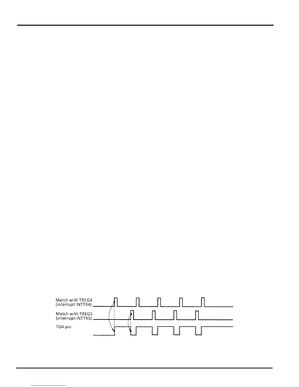
TMP96C141AF
76543210
TRUN ← –x–0–––– Stop timer 4.
P8CR ← –––––––0 Set P80 to input mode.
INTET54 ← 11001000 Enable INTTR5 and sets interrupt level 4, while
disables INTTR4.
T4FFCR ← 11000011 Disable trigger.
T4MOD ← 00100100 Select TI4 as the input clock.
TREG5 ← ******** Set the number of counts (16 bits).
TRUN ← 1x–1–––– Start timer 4.
Note: When used as an event counter, set the prescaler in RUN mode.
(3) 16-bit Programmable Pulse Generation (PPG) Output
Mode
flip-flop TFF4 that is to be enabled by the match of the
up-counter UC4 with the timer register TREG4 or 5
and to be output to TO4 (also used as P82). In this
Since both timers operate in exactly the same way,
mode, the following conditions must be satisfied.
timer 4 is used for the purposes of explanation.
The PPG mode is obtained by inversion of the timer
76543210
TRUN ← –x–0–––– Stop timer 4.
TREG4 ← ******** Set the duty (16 bits).
TREG5 ← ******** Set the cycle (16 bits).
T45CR ← 0xxx –––1 Double buffer of TREG4 enable.
(Changes the duty and cycle at the interrupt INTTR5)
T4FFCR ← 11001100 Set the mode to invert TFF4 at the match with
TREG4/TREG5, and also sets TFF4 to “0”.
T4MOD ← 001001** Select internal clock for input and disables the capture function.
(** = 01, 10, 11)
P8CR ← –––––1––
P8FC ← x–xx–1xx
TRUN ← 1x–1–––– Start timer 4.
Assign P82 as TO4.
)
(Set value of TREG4) < (Set value of TREG5)
Note: x; don’t care –; no change
Figure 3.9 (11). Programmable Pulse Generation (PPG) Output Waveforms
96 TOSHIBA CORPORATION
Page 97
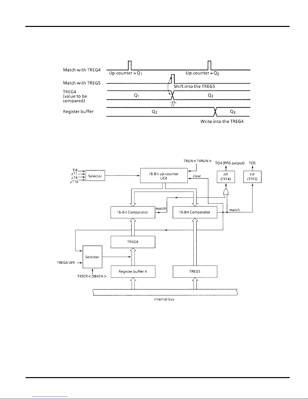
TMP96C141AF
When the double buffer of TREG4 is enabled in this
mode, the value of register buffer 4 will be shifted in TREG4
Figure 3.9 (12). Operation of Register Buffer
Shows the block diagram of this mode.
at match with TREG5. This feature makes easy the handling of
low duty waves.
Figure 3.9 (13). Block Diagram of 16-Bit PPG Mode
TOSHIBA CORPORATION 97
Page 98
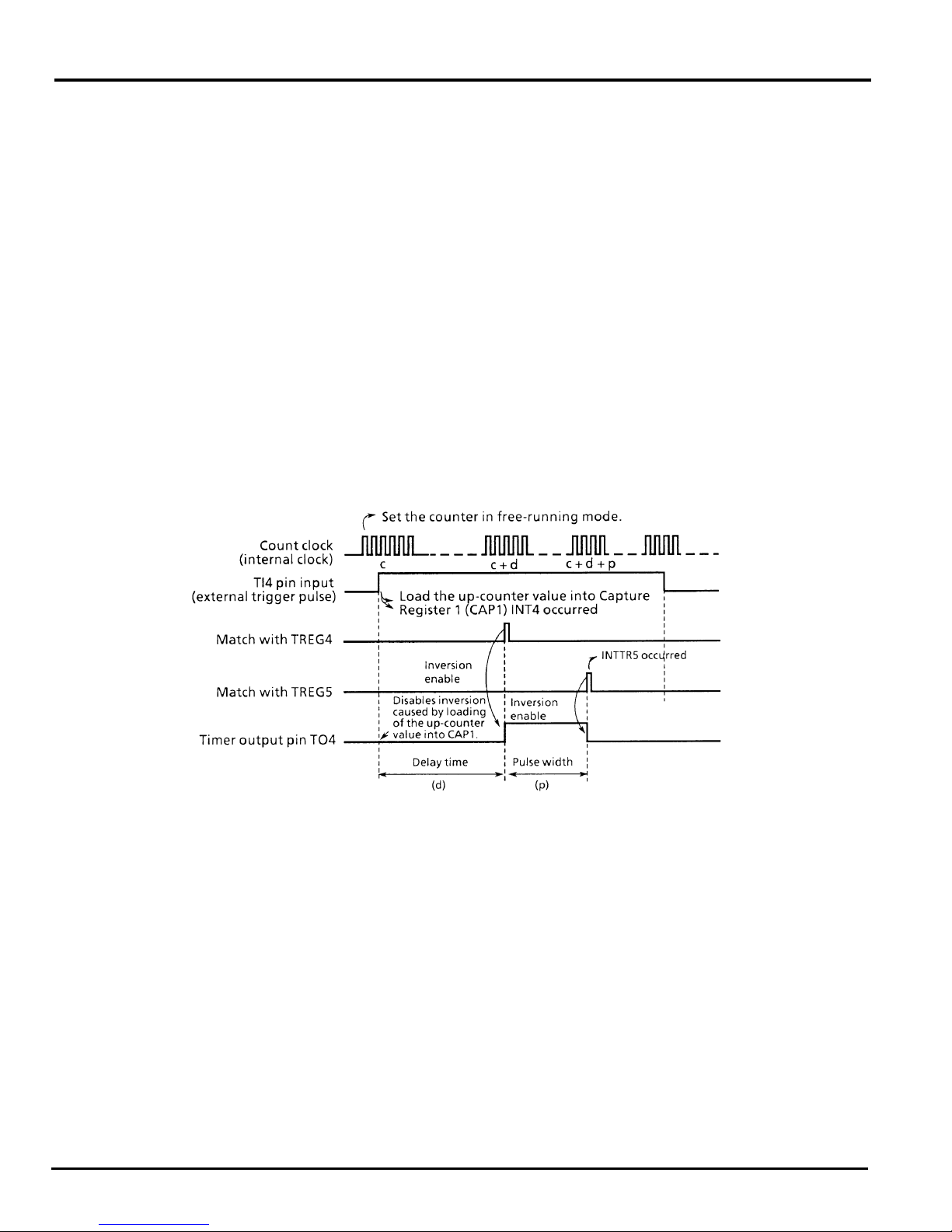
TMP96C141AF
(4) Application Examples of Capture Function
The loading of up-counter (UC4) values into the capture registers CAP1 and CAP2, the timer flip-flop TFF4
inversion due to the match detection by comparators
CP4 and CP5, and the output of TFF4 status to TO4
pin can be enabled or disabled. Combined with interrupt function, they can be applied in many ways, for
example:
➀ One-shot pulse output from external trigger pulse
➁ Frequency measurement
➂ Pulse width measurement
➃ Time difference measurement
➀ One-Shot Pulse Output from External Trigger Pulse
Set the up-counter UC4 in free-running mode with the
internal input clock, input the external trigger pulse
from TI4 pin, and load the value of up-counter into
capture register CAP1 at the rise edge of the TI4 pin.
Then set to T4MOD <CAP12M1, 0> = 01.
When the interrupt INT4 is generated at the rise edge
of TI4 input, set the CAP1 value (c) plus a delay time (d)
to TREG4 (= c + d), and set the above set value (c + d)
plus a one-shot pulse width (p) to TREG5 (= c + d + p).
When the interrupt INT4 occurs the T4FFCR <EQ5T4,
EQ4T4> register should be set that the TFF4 inversion
is enabled only when the up-counter value matches
TREG4 or TREG5. When interrupt INTTR5 occurs, this
inversion will be disabled.
Figure 3.9 (14). One-Shot Pulse Output (with Delay)
98 TOSHIBA CORPORATION
Page 99
Setting Example: To output 2ms one-shot pulse with 3ms delay to the external trigger pulse to TI4 pin.
Keep counting (Free-running).
Main setting
T4MOD ← ––101001
T4FFCR ← 11000010
P8CR ← –––––1––
P8FC ← x–xx–1xx
INTE45 ← ––––1100 Enable INT4, and disables INTTR4 and INTTR5.
INTET54 ← 10001000
TRUN ← 1x–1–––– Start timer 4.
Setting of INT4
TREG4 ← CAP1 + 3ms/φT1
φ
TREG5 ← TREG4 + 2ms/
T4FFCR ← ––––11––
INTET54 ← 1100–––– Enable INTTR5.
T1
Count with φT1.
Load the up-counter value into CAP1 at the rise edge of TI4 pin input.
Clear TFF4 to zero.
Disable TFF4 inversion.
Select P82 as the TO4 pin.
)
Enable TFF4 inversion when the up-counter value matches TREG4 or 5.
TMP96C141AF
Setting of INT5
T4FFCR ← ––––00––
Disable TFF4 inversion when the up-counter value matches TREG 4 or 5.
INTET54 ← 1000–––– Disable INTTR5.
Note: x; don’t care –; no change
When delay time is unnecessary, invert timer flip-flop
TFF4 when the up-counter value is loaded into capture register
1 (CAP1), and set the CAP1 value (c) plus the one-shot pulse
inversion should be enabled when the up-counter (UC4) value
matches TREG5, and disabled when generating the interrupt
INTTR5.
width (p) to TREG5 when the interrupt INT4 occurs. The TFF4
TOSHIBA CORPORATION 99
Page 100
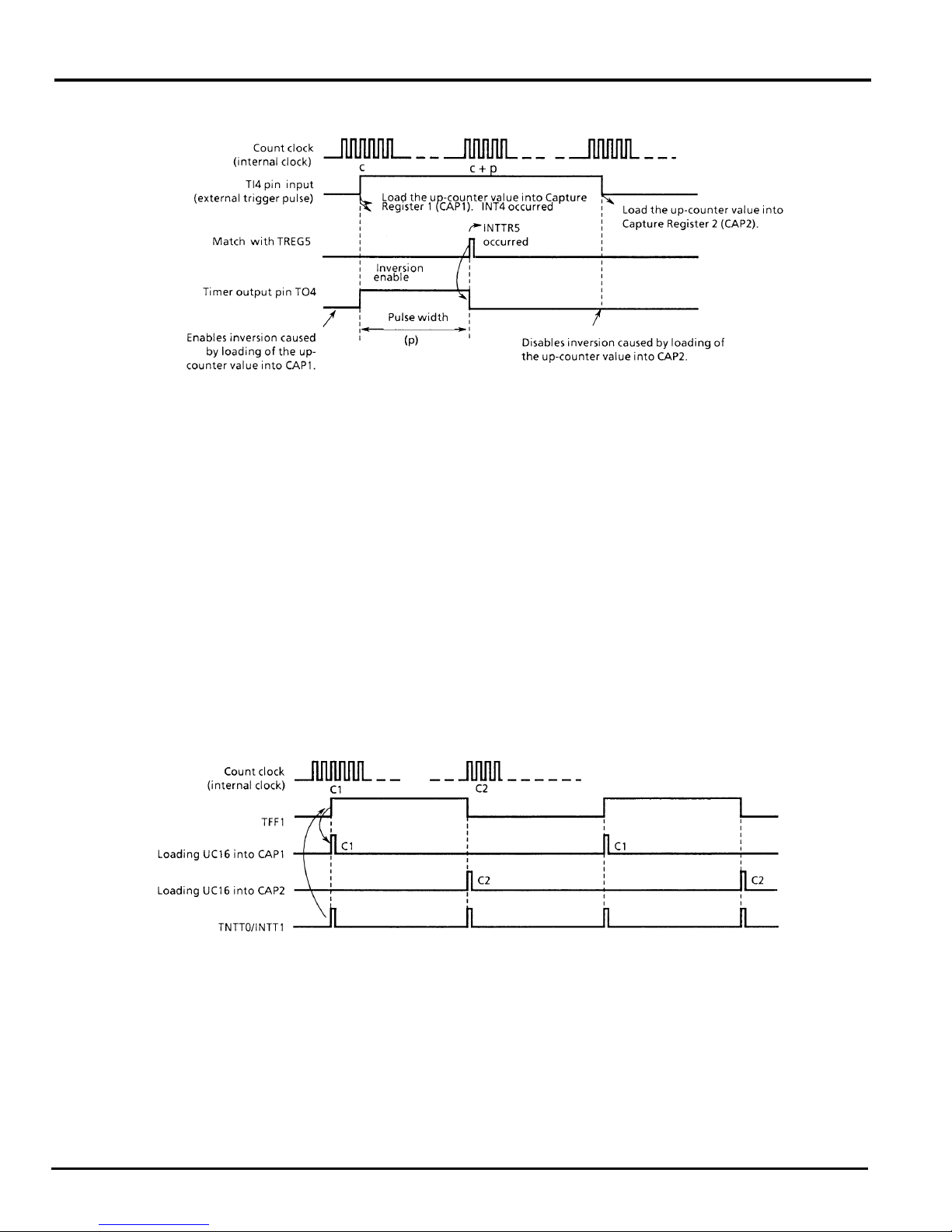
TMP96C141AF
Figure 3.9 (15). One-Shot Pulse Output (without Delay)
➁ Frequency Measurement
The frequency of the external clock can be measured
in this mode. The clock is input through the TI4 pin, and
its frequency is measured by the 8-bit timers (Timer 0 and
Timer 1) and the 16-bit timer/event counter (Timer 4).
The TI4 pin input should be selected for the input
clock of Timer 4. The value of the up-counter is loaded
into the capture register CAP1 at the rise edge of the
timer flip-flop TFF1 of 8-bit timers (Timer 0 and Timer 1),
and into CAP2 at its fall edge.
The frequency is calculated by the difference
between the loaded values in CAP1 and CAP2 when the
interrupt (INTT0 or INTT1) is generated by either 8-bit
timer.
Figure 3.9 (16). Frequency Measurement
For example, if the value for the level “1” width of
TFF1 of the 8-bit timer is set to 0.5 sec. and the differ-
100 TOSHIBA CORPORATION
ence between CAP1 and CAP2 is 100, the frequency will
be 100/0.5 [sec.] = 200 [Hz].
 Loading...