

Page 1

REV2.6 July. 12, 2002
Rev. 2.6 12/July/2002
16bit Micro controlle
r
TLCS-900/L1 series
TMP91C824F
Data Book
Page 2

contents
Table of Contents
TLCS-900/L1 Devices
TMP91C824F
1. OUTLINE AND DEVICE CHARACTERISTICS ……………………… 91C824-1
2. PIN ASSIGNMENT AND PIN FUNCTIONS ……………………… 91C824-4
3. OPERATION ……………………………………………………… … 91C824-9
3.1 CPU …………………………………………………………………… 91C824-9
3.2 Memory Map ………………………………………………………… 91C824-11
3.3 Triple clock, Stand-by function, Noise reduction ………………………… 91C824-12
3.4 Interrupts …………………………………………………………………… 91C824-36
3.5 Functions of Ports …………………………………………………………… 91C824-51
3.5.1 Port 1 ……………………………………………………………… 91C824-55
3.5.2 Port 2 ……………………………………………………………… 91C824-56
3.5.3 Port 5 ……………………………………………………………… 91C824-58
3.5.4 Port 6 ……………………………………………………………… 91C824-61
3.5.5 Port 7 ………………………… …………………………………… 91C824-62
3.5.6 Port 8 ……………………………………………………………… 91C824-66
3.5.7 Port B ……………………………………………………………… 91C824-67
3.5.8 Port C ……………………………………………………………… 91C824-70
3.5.9 Port D ……………………………………………………………… 91C824-73
3.6 Chip Select / Wait Controller ……………………………………………… 91C824-78
3.7 8-bit Timers(TMRA) ……………………………………………………… 91C824-88
3.8 Memory Management Unit ……………………………………………… 91C824-108
3.9 Serial Channel ……………………………………………………………… 91C824-119
3.10 Serial Bus Interface ………………………………………………………… 91C824-151
3.11 Analog / Digital Converter ………………………………………………… 91C824-179
3.12 Watch Dog Timer ………………………………………………………… 91C824-189
3.13 RTC ………………………………………………………………………… 91C824-195
3.14 Melody / Alarm Generator ………………………………………………… 91C824-209
4. ELECTRICAL CHARACTERISTICS ………………… …… 91C824-215
5. TABLE OF SFR ……………………………………………………… … 91C824-227
8. PACKAGES …………………………………………………………… ……… 91C824-252
Page 3
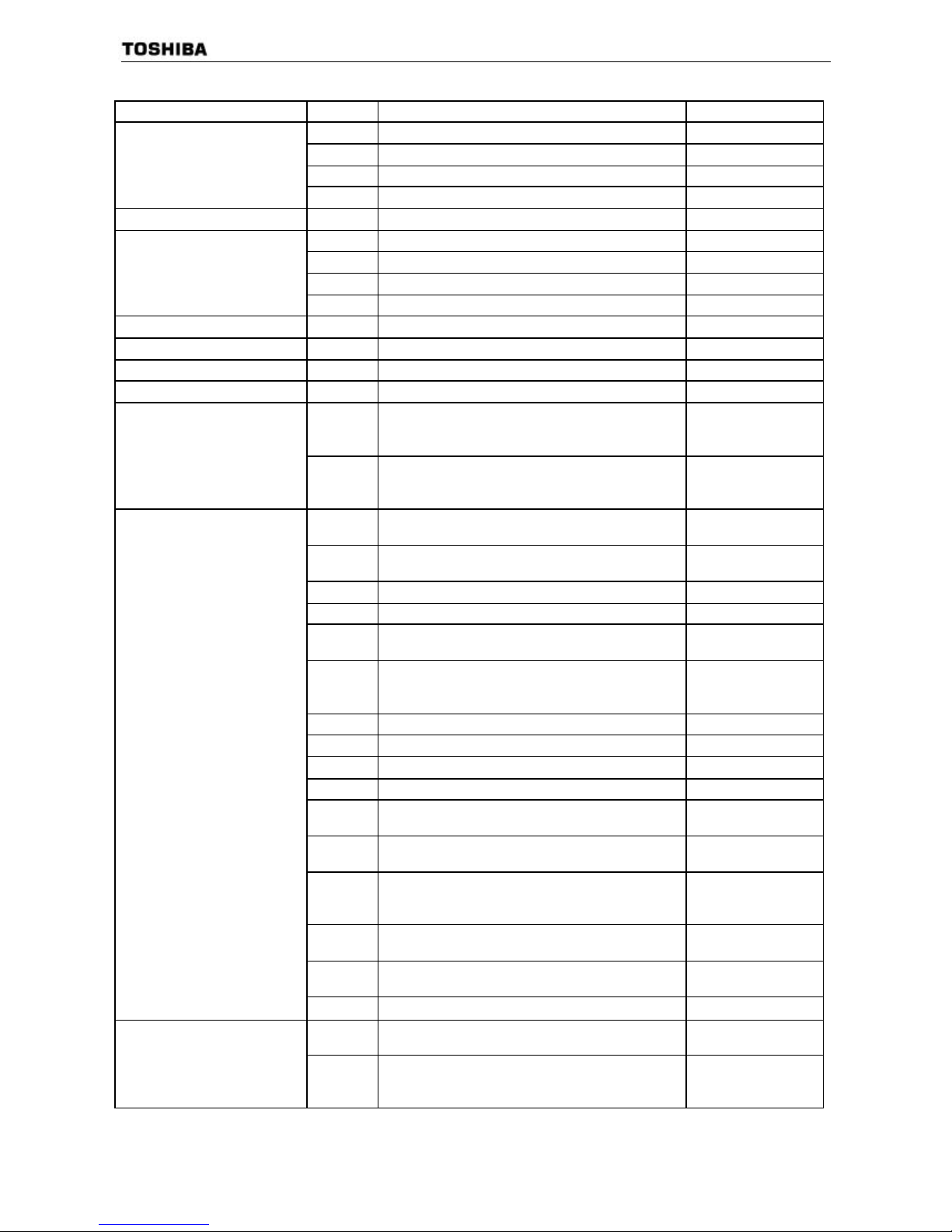
Data Book modification history
Rev./Date page Modification item Reason
109 Bank Operation S/W Example in MMU
218 Recommended Crystal oscillation Circuit
165 Stop condition generation
Rev12/Mar-15-2001
166 Timing diagram for TMP91C824 Restart
Rev14/July-16-2001 12-24 DFM(triple cock modify)
17,240 EMCCR3
159,168 Add ed the sentence and diagram at SBI
155 Modify bit6(TRX)
Rev14/July-26-2001
114 Added the diagram and sentence of MMU
Rev21/August -21-2001 14 CPU: modify the figure
Rev22/September -21-2001 222 Electric Specification
Rev22/September -7-2001 226 Murata factory URL added
Rev23/October-26-2001 217 33MHZ AC added
216 Syntax err
“2V SLOW ICC” -> “2V NORMAL ICC”
Unit “uA” -> “mA”
Rev24/January-18-2002
221 Spec modify
AD converter
IREF max 1.20mA -> 1.35mA
contents Remove “TENTATIVE” of ELECTRICAL
CHARACTERISTICS
1 Add the comment about JTMP91C824
Modify the frequency of Micro DMA
Change the
reference
2 Add the comment about package Mistake
16,240 Modify the input frequency of (DFMCR1) Mistake
29 Modify the name SBI0BR1à SBI0BR0 in the
table 3.3.2
Mistake
30,251 Add the limitation about HALT mode Mistake
*Important
matter
48,236 Add the comment to the register IIMC bit6 Mistake
55 Modify the comment in the figure Mistake
87 Add the figure for connecting SRAM Shortage
97,98 Modify WàR/W and remove the note Mistake
100,104
106
Modify the name of the register in the
program P7àPB
Mistake
146 Modify the name of the register in the
program P9àPC
Mistake
208 Add the limitation about RTC Mistake
*Important
matter
212 Modify the name of scale in the table Change
expression
226 Change the comment about MURATA at
the bottom
Change
expression
Rev2.5/June-21-2002
240 Remove the note Mistake
15,239 Add the word “IDLE1” to the bit0 of
(SYSCR2) register
Mistake Rev2.6/July-12-2002
30,251 Add the INTALM0 to 4 in the (note) Mistake
※Each page number depends on the revision when it’s made.
Page 4

TMP91C824
91C824-1
CMOS 16-Bit Microcontrollers
TMP91C824F/JTMP91C824-S
1. OUTLINE AND FEATURES
TMP91C824F is a high-speed 16-bit microcontroller designed for the control of various mid- to large-scale
equipment.
TMP91C824F comes in a 100-pin fla t package and a 100-p ad Dice form. JTMP91C824-S is a chip form
product.
Listed below are the features.
(1) High-speed 16-bit CPU (900/L1 CPU)
• Instruction mnemo nics are upward-compatible with TLCS-9 0
• 16 Mbytes of linear address space
• General-purpose registers and register banks
• 16-bit multiplication and division instructions; bit transfer and arithmetic instructions
• Micro DMA: 4 channels (0.5 µs/2 bytes at 33 MHz)
(2) Minimum instruction execution time: 121 ns (at 33 MHz)
(3) Built-in RAM: 8 Kbytes
Built-in ROM: No ne
(4) External memory expansion
• Expandable up to 106M bytes (shared program/data area)
• Can simultaneously support 8-/16-bit width external data bus
… Dynamic data bus syzing
• Separate bus system
(5) 8-bit timers: 4 channels
(6) General-purpose serial interface: 2 channels
• UART/Synchronous mode: 2 channels
• IrDA Ver.1.0 (115.2kbps) mode selectable: 1 channel
(7) Serial bus interface: 1 channel
• I2C bus mode/clock synchronous mode selectable
Purchase of TOSHIBA I2C components conveys a license under the Philips I2C Patent Ri ght s to u s e thes e c omp on en t s in a
n
I2C system, pr ovided that the syst em conforms to the I2C Standard Specification as defined by Philips.
• For a discussion of how the reliability of microcontrollers can be predicted, please refer to Section 1.3 of the chapter entitled Quality and
Reliability Assu rance / Handling Precautions.
• TOSHIBA is cont inu ally work i n g to imp rove t h e quali t y and th e reli abi li ty of it s pr oduct s . Neverth eles s, semi cond uc t or devic es in gen era l can
malfunction or fail due to their inherent electrical sensitivity and vulnerability to physical stress. It is the responsibility of th e buyer, when
utilizing TOSHIBA products, to observe standards of safety, and to avoid situations in which a malfunction or failure of a TOSHIBA product
could cause loss of human life, bod ily injury or damage to property. In developing your designs, please e ns ure that TOSHIBA pro ducts are used
within specified operating ranges as set forth in the most recent products specifications. Also, please keep in mind the precautions and conditions
set forth in the TOSHIBA Semiconductor Reliab ility Handbook.
• The products described in this document are subject to foreign exchange and foreign trade laws.
• The informa tion conta ined herei n is present ed only as a gu ide for the app lica tions of ou r product s. No responsi bilit y is assum ed by TOSHIBA
CORPORATION for any infrin gement s of intellec tua l prop erty or other righ ts of th e third pa rties whic h may resu lt from it s use. No li cense is
granted by implication or otherwise under any intellectual property or other rights of TOSHIBA CORPORATION or others.
• The information contained herein is subject to change without notice.
980508TBA1
Page 5

TMP91C824
91C824-2
(8) Timer for real-time clock (RTC)
• Based on TC8521A
(9) 10-bit A/D converter : 8 channels
(10) Watch dog timer
(11) Melody/Alarm generator
• Melody: Output of clock 4 to 5461Hz
• Alarm: Output of the 8 kinds of alarm pattern
• Output of the 5 kinds of interval interrupt
(12) Chip select/Wait controller: 4 channels
(13) Memory Management Unit
• Expandable up to 106M bytes (4 local area/8bank method)
(14) Interrupts: 37 interrupts
• 9 CPU interrupts: So ft ware interrupt instruction and illegal instruction
• 23 internal interrupts: 7 priority levels are selectable
• 5 external interrupts: 7 priority levels are selectab le ( among 4 interrupts are selectable
edge mode)
(15) Input/output ports: 35 pins (@External 16-bit data bus memory)
(16) Stand-by function
Three Halt modes: Idle2 (programmable), Idle1 and Stop
(17) Triple-clock controller
• Clock doubler (DFM) circuit is inside
• Clock gear function: Select a High-frequency clock fc/1 to fc/16
• RTC (fs=32.768kHz)
(18) Opera ting voltage
• VCC = 2.7 V to 3.6 V (fc max = 33 MHz)
• VCC = 1.8 V to 3.6 V (fc max = 10 MHz)
(19) Package
• 100-pin QFP: LQFP100 - P -1414 - 0.5D
• Chip form supply also available. For details, contact your local Toshiba sales
representative.
Page 6
TMP91C824
91C824-3
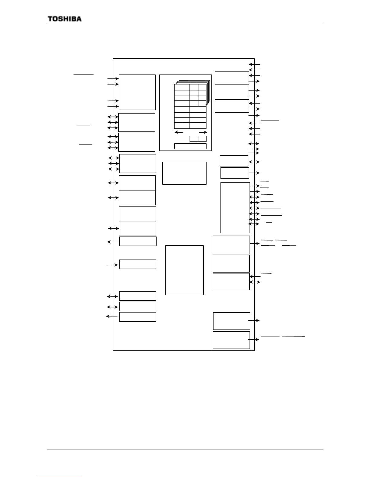
Figure 1.1 TMP91C824F Block Diagram
8KB RAM
CPU (TLCS-900/L1)
PC
10-BIT 8CH
A/D
CONVERTER
H-OSC
SIO/UART/IrDA
(SIO0)
8BIT T IME R
(TMR A 0 )
32 bit
F
SR
XWA
XB C
XDE
XHL
XIX
XIY
XIZ
XS P
W A
IX
IY
IZ
SP
TXD0 (PC0
)
RXD0 (PC1
)
TXD1 (PC3
)
RXD1 (PC4)
DVCC [3]
DVSS [3]
X1
X2
D0 to D7
A0 to A7
A8 to A15
P10 to P17(D8 to D15)
P20 to P27
(A16 toA23)
A
N0 to AN7
(P80 to P87)
AVCC, AVSS
VREFH, VREFL
SCOUT(PD5)
RESET
AM0
AM1
WDT
(Watch
DogTimer)
Clock Gear,
Clock Doubler
SIO/UART
(SIO1)
RD
WR
HWR(P 52)
WAIT (P53)
BUSRQ (P54)
BUSAK(P55)
R/W (P56)
L-OSC
EMU0
EMU1
PORT 5
CS/WAIT
CONTRO LLER
(4-BLOCK)
PORT 2
CS0 toCS 3
,CS2A〜CS2E
INTERRUPT
CONTRO LLER
INT0 to INT 3
MELOD Y/
ALARM-OUT
MLDALM(PD7)
8BIT T IME R
(TMR A 1 )
TA1OUT (PB1)
8BIT TIMER
(TMR A 2 )
8BIT TIMER
(TMR A 3 )
TA3OUT (PB2
)
( ) : In iti al Function Aft er Reset
B C
D E
H L
ADTRG(P83)
SCLK1/ CTS1(PC5
)
(P60 to P67)
PORT 1
PORT 6
PORT 8
PORT B
PORT C
PORT D
(PB3 to PB6),
SCLK0/CTS0 (PC2)
OPTRX0,SCK (P70
)
OPTTX0,SO/SDA
(P71)
SERIAL BUS
I/F(SBI)
SI/SCL
(P72
)
RTC
ALARM,MLDALM(PD6)
XT1
XT2
TA0IN (PB0)
NMI
MMU
Page 7
TMP91C824
91C824-4
2. PIN ASSIGNMENT AND PIN FUNCTIONS
The assignment of input/output pins for the TMP91C824F, their names and functions are as follows:
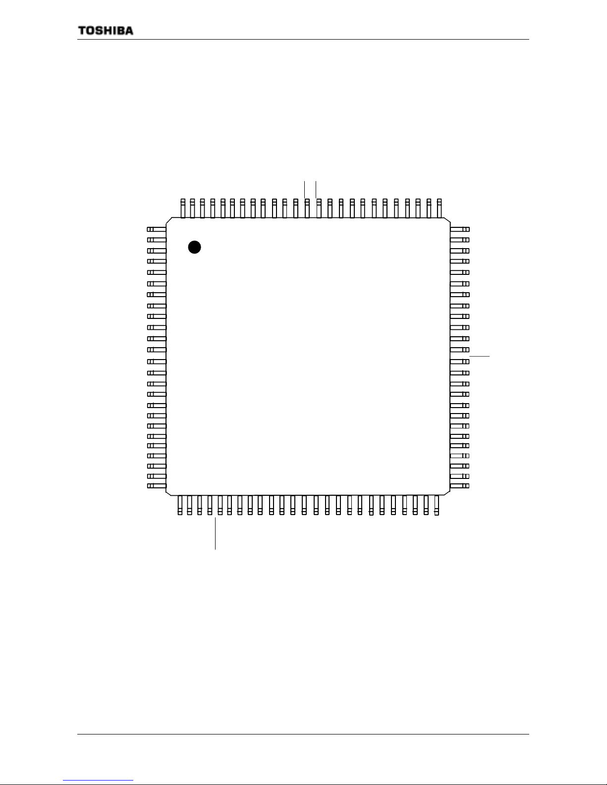
2.1 Pin Assignment Diagram
Figure 2.1.1 shows the pin assignment of the TMP91C824F.
VREFL
TMP91C824
QFP100
TOPVIEW
1
5
10
15
20
25
30
35
40
45
50
55
60
65
70
75
80
85
90
95
100
A VSS
P80/AN0
P81/AN1
P82/AN2
P83/AN3/ADTRG
P84/AN4
P85/AN5
P86/AN6
P87/AN7
AVCC
P70/SCK/OPTRX0
P71/S0/SDA/OPTTX0
P72/SI/SCL
TA0IN/PB0
TA1OUT/PB1
TA3OUT/PB2
INT0/PB3
INT1/PB4
INT2/PB5
INT3/PB6
P55/BUSAK
DVCC1
A1 1
A12
A13
A14
A15
P20/A16
P21/A17
P22/A18
P23/A19
P24/A20
P25/A21
DVCC2
NMI
DVSS2
P26/A22
P27/A23
P17/D15
P16/D14
P15/D13
P14/D12
P13/D11
P12/D10
P1 1/D9
P10/D8
D7
D6
D5
D4
D3
D2
D1
D0
PD7/MLDALM
PD6/ALARM/MLDALM
PD5/SCOUT
SCLK1/CTS1/PC5
RXD1/PC4
TXD1/PC3
SCLK0/CTS0/PC2
RXD0/PC1
TXD0/PC0
EMU1
EMU0
XT2
XT1
RESET
AM1
X1
DVSS1
X2
P64/EA24/CS2B
P56/WAIT
P65/EA25/CS2C
P63/CS3
P62/CS2/CS2
A
P61/CS1
P60/CS0
P67/CS2E
PZ3/R/W
PZ2/HWR
WR
RD
A0A1A2A3A4A5A6A7A8A
9
VREFH
AM0
A
10
P66/CS2D
P54/BUSRQ
Figure 2.1.1 Pin assignment diagram (100-pin QFP)
Page 8
TMP91C824
91C824-
5
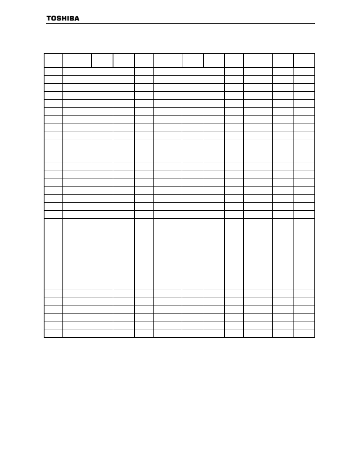
2.2 Pad Layout
(Chip size 4.37mm ×4.37mm) unit (μm)
PIN
no
Name X
point Y point
PIN
No
Name X
point Y point
PIN
No
Name X
point Y point
1 VREFL -2050 1721 35 PC0 -140 -2050 69 P21 2045 939
2 AVSS -2050 1596 36 PC1 -14 -2050 70 P20 2045 1075
3 AVCC -2050 1470 37 PC2 112 -2050 71 A15 2045 1207
4 P80 -2050 1337 38 PC3 238 -2050 72 A14 2045 1337
5 P81 -2050 1209 39 PC4 365 -2050 73 A13 2045 1464
6 P82 -2050 1076 40 PC5 491 -2050 74 A12 2045 1592
7 P83 -2050 943 41 PD5 618 -2050 75 A11 2045 1721
8 P84 -2050 810 42 PD6 744 -2050 76 A10 1720 2045
9 P85 -2050 677 43 PD7 871 -2050 77 A9 1591 2045
10 P86 -2050 544 44 D0 998 -2050 78 A8 1464 2045
11 P87 -2050 416 45 D1 1124 -2050 79 A7 1337 2045
12 P70 -2050 148 46 D2 1251 -2050 80 A6 1197 2045
13 P71 -2050 15 47 D3 1377 -2050 81 A5 1058 2045
14 P72 -2050 -118 48 D4 1504 -2050 82 A4 918 2045
15 PB0 -2050 -251 49 D5 1630 -2050 83 A3 778 2045
16 PB1 -2050 -384 50 D6 1757 -2050 84 A2 639 2045
17 PB2 -2050 -517 51 D7 2045 -1750 85 A1 499 2045
18 PB3 -2050 -650 52 P10 2045 -1614 86 A0 359 2045
19 PB4 -2050 -783 53 P11 2045 -1478 87 /RD 219 2045
20 PB5 -2050 -916 54 P12 2045 -1341 88 /WR 80 2045
21 PB6 -2050 -1049 55 P13 2045 -1205 89 PZ2 -59 2045
22 P54 -2050 -1182 56 P14 2045 -1069 90 PZ3 -199 2045
23 P55 -2050 -1315 57 P15 2045 -933 91 P56 -338 2045
24 AM0 -2050 -1448 58 P16 2045 -796 92 P60 -478 2045
25 VCC -2050 -1581 59 P17 2045 -660 93 P61 -618 2045
26 X2 -1551 -2050 60 P27 2045 -524 94 P62 -757 2045
27 VSS -1330 -2050 61 P26 2045 -388 95 P63 -897 2045
28 X1 -1205 -2050 62 VSS 2045 -234 96 P64 -1037 2045
29 AM1 -1075 -2050 63 /NMI 2045 -80 97 P65 -1176 2045
30 /RESET -948 -2050 64 VCC 2045 240 98 P66 -1316 2045
31 XT1 -822 -2050 65 P25 2045 394 99 P67 -1456 2045
32 XT2 -520 -2050 66 P24 2045 530 100 VREFH -1725 2045
33 EMU0 -394 -2050 67 P23 2045 666
34 EMU1 -267 -2050 68 P22 2045 803
Page 9
TMP91C824
91C824-6
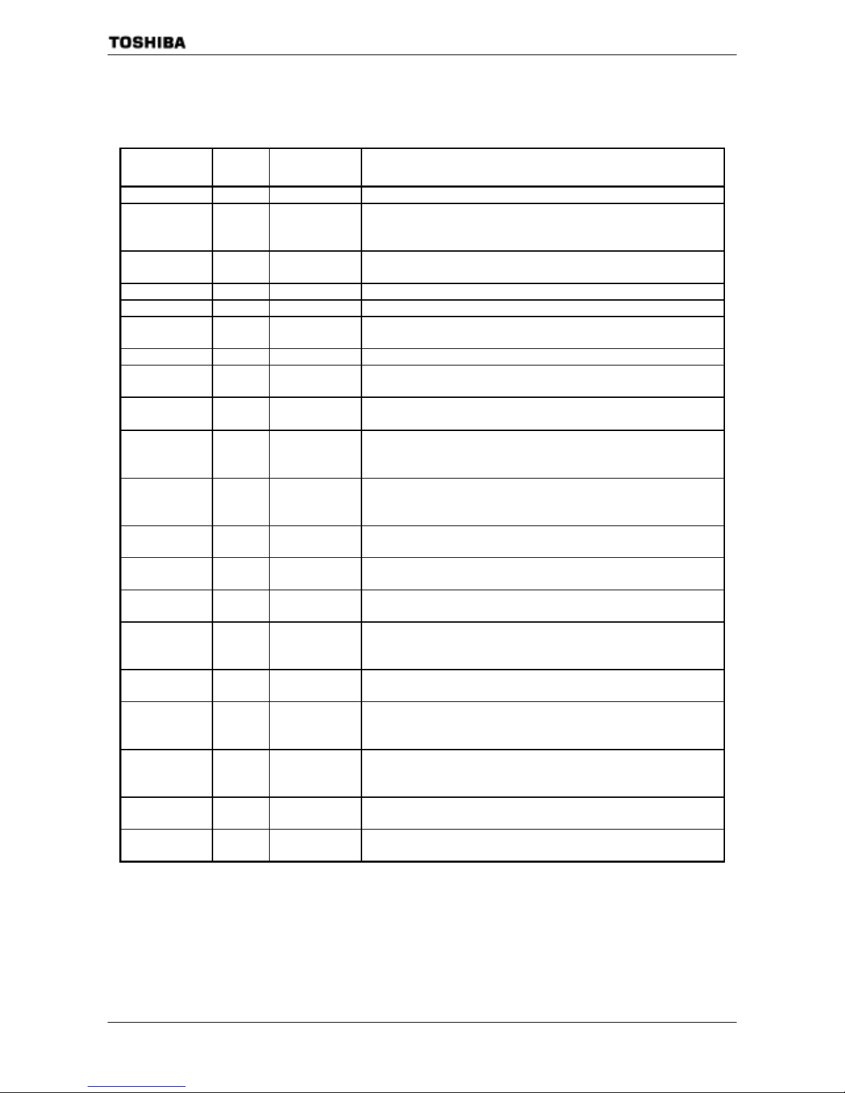
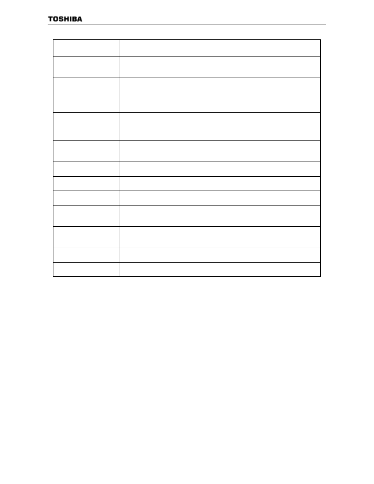
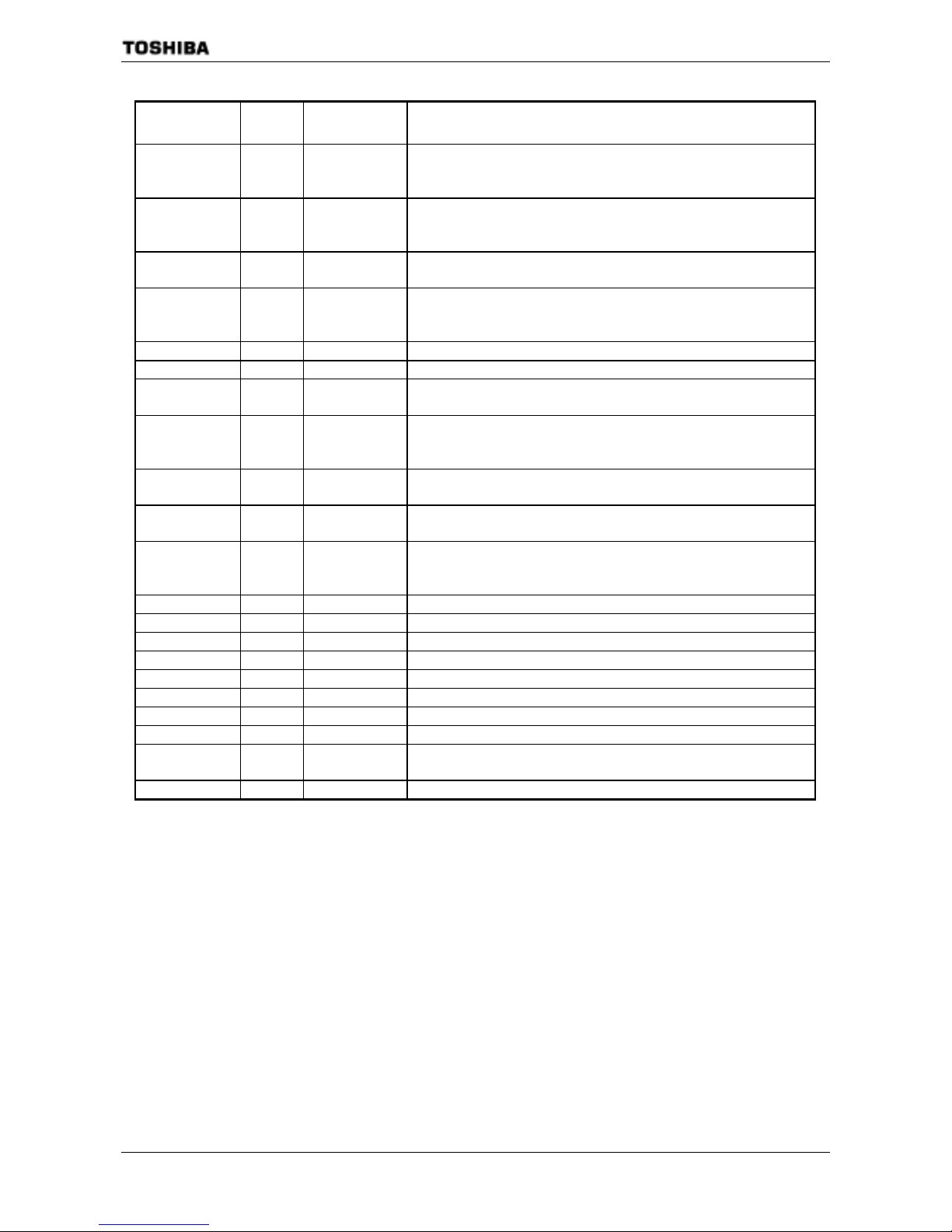
2.3 Pin Names and Functions
The names of the input/output pins and their functions are described below.
Table 2.2 Pin names and functions.
Pin Name
Number
of Pins
I/O Functions
D0 to D7
8
I/O Data (lower): b its 0 to 7 of data bus
P10 to P17
D8 to D15
8
I/O
I/O
Port 1: I/O port that allows I/O to be selected at the bit level
(When used to the external 8bit bus)
Data (upper): bits 8 to15 of data bus
P20 to P27
A16 to A23
8
Output
Output
Port 2: Output port
Address: bits 16 to 23 of address bus
A8 to A15
8
Output Address: bits 8 to 15 of address bus
A0 to A7
8
Output Address: bits 0 to 7 of address bus
/RD
1
Output Read: strobe signal for reading external memory
/WR
1
Output Writ e: strobe signal for writing data to pins D0 to D7
PZ2
/HWR
1
I/O
Output
Port Z2: I/O port (with pull-up resistor)
High Write: strobe signal for writing data to pins D8 to D15
PZ3
____
R/W
1
I/O
Output
Port Z3: I/O port (with pull-up resistor)
P54
/BUSRQ
1
I/O
Input
Port 54: I/O port (with pull-up resi stor)
Bus Request: High-Impedance used to request Bus Release
Read/Write: 1 represent s Read or Dummy cycle; 0 represent s write cycle.
P55
/BUSAK
1
I/O
Output
Port 55: I/O port (with pull-up resi stor)
Bus Acknowledge: signal used to acknowledge Bus Release
P56
/WAIT
1
I/O
Input
Port 56: I/O port (with pull-up resi stor)
Wait: pin used to request CPU bus wait
P60
/CS0
1
Output
Output
Port 60:Output port
Chip select 0: Outputs “0” when address is within specified address area.
P61
/CS1
1
Output
Output
Port 61:Output port
Chip Select 1: outputs “0” when address is within specified address area
P62
/CS2
/CS2A
1
Output
Output
Output
Port 62: Output port
Chip Select 2: outputs “0” when address is within specified address area
Expand Chip Select: 2A: outputs 0 when address is within specified address area
P63
/CS3
1
Output
Output
Port 63:Output port
Chip Select 3: outputs “0” when address is within specified address area
P64
EA24
/CS2B
1
Output
Output
Output
Port 64: Output port
(Address 24: Expand address)
(Expand Chip Select: 2B: outputs “0” when address is within specified address area)
P65
EA25
/CS2C
1
Output
Output
Output
Port 65: Output port
(Address 25: Expand address)
(Expand Chip Select: 2B: outputs “0” when address is within specified address area)
P66
/CS2D
1
Output
Output
Port 66: Output port
(Expand Chip Select: 2D: outputs “0” when address is within specified address area)
P67
/CS2E
1
Output
Output
Port 67: Output port
(Expand Chip Select: 2E: outputs “0” when address is within specified address area)
.
Page 10
TMP91C824
91C824-
7
Pin Name Number
of Pins
I/O Functions
P70
SCK
OPTRX0
1
I/O
I/O
Input
Port 70: I/O port
Serial bus interface clock I/O data at SIO mode
Serial recive data “0”
P71
S0
SDA
OPTTX0
1 I/O
Output
I/O
Output
Port 71: I/O port
Serial bus interface send data at SIO mode
Serial bus interface send/recive data at I2C mode
Open drain output mode by programmable (with pull up)
Serial send data “0”
P72
SI
SCL
1 I/O
Input
I/O
Port 72I/O port
Serial bus interface recive data at SIO mode
Serial bus interface clock I/O data at I2C mode
Open drain output mode by programmable (with pull up)
P80 to P87
AN0 to AN7
/ADTRG
8 Input
Input
Input
Port 80 to 87 port: Pin used to input ports
Analog input 0 to 7: Pin used to Input to A/D conveter
A/D trigger: Signa l used to request A/D start (with used to P83)
PB0
TA0IN
1 I/O
Input
Port B0: I/O port
8bit timer 0 input: Timer 0 input
PB1
TA1OUT
1 I/O
Output
Port B1: I/O port
8bit timer 1 output: Timer 0 input or Timer 1 output
PB2
TA3OUT
1 I/O
Output
Port B2: I/O port
8bit timer 3 output: Timer 2 input or Timer 3 output
PB3
INT0
1 I/O
input
Port B0: I/O port
Interrupt request pin0: Interrupt request pin with programmable level / rising /
falling edge
PB4 to PB6
INT1 to INT3
3 I/O
input
Port B4 to B6: I/O port
Interrupt request pin1 to 3: Interrupt request pin with programmable level / rising
/falling edge
PC0
TXD0
1 I/O
Output
Port C0: I/O port
Serial 0 send data: Open drain output pin by programmable
PC1
RXD0
1 I/O
Input
Port C1: I/O port
Serial 0 recive data
Page 11
TMP91C824
91C824-8
Pin Name Number
of Pins
I/O Functions
PC2
SCLK0
/CTS0
1 I/O
I/O
Input
Port C2: I/O port
Serial clock I/O 0
Serial data send enable 0 (Clear to Send )
PC3
TXD1
1 I/O
Output
Port C3: I/O port
Serial send data 1
Open drain outpu t pi n by programma bl e
PC4
RXD1
1 I/O
Input
Port C4: I/O port
Serial recive data 1
PC5
SCLK1
/CTS1
1 I/O
I/O
Input
Port C5: I/O port
Serial clock I/O 1
Serial data send enable 1 (Clear to Send )
XT1 1 Input Low Frequency Oscillator connecting pin
XT2 1 Output Low Frequency Oscillator connecting pin
PD5
SCOUT
1 Output
Output
Port D5: Output port
System clock output : f
SYS
or fS output
PD6
/ALARM
/MLDALM
1 Output
Output
Output
Port D6: Output port
RTC alarm output pin
PD7
MLDALM
1 Output
Output
Port D7: Output port
Melody / Alarm outpu t pin
/NMI
1 Input Non-Maskable Interrupt Request Pin: interrupt request pin with programmable
falling edge level or with both edge le vels programmable
AM0 to 1
2 Input Operation mode:
Fixed to AM1=”0”,AM0=”1” 16-bit external bus or 8/16-bit dynamic sizing.
Fixed to AM1=”0”,AM0=”0” 8-bit external bus fixed.
EMU0 1 Output Open pin
EMU1 1 Output Open pin
/RESET 1 Input Reset: initializes TMP91C824. (With pull-up resistor)
VREFH 1 Input Pin for reference voltage input to AD converter (H)
VREFL 1 Input Pin for reference voltage input to AD converter (L)
AVCC 1 High-frequency oscillator connection pins
AVSS 1 Power supply pin for AD converter
X1/X2 2 GND pin for AD converter (0 V)
DVCC 3 Power supply pins (All Vcc pins should be connecyed with the power
Supply pin).
DVSS 3 GND pins (0 V) (All pins shuold be connected with GND(0V).
Page 12

TMP91C824
91C824-9
3. OPERATION
This following describes block by block the functions and operation of the TMP91C824 F.
Notes and restrictions for eatch book are outlined in “ 7, Precautions and Restrictions at the end of this manual.
3.1 CPU
The TMP91C824 incorporates a high-performance 16 -bit CPU (the 900/L1-CPU). For CPU operation, see
the “TLCS-900/L1 CPU”.
The following describe the unique function of the CPU used in the TMP91C824; these functions are not
covered in the TLCS-900/L1 CPU section.
3.1.1 Reset
When resetting the TMP91C824 microcontroller, ensure that the power supply voltage is within the
operating voltage range, and that the internal high-frequency oscillator has stabilized. Then hold the
/RESET input to Low level at least for 10 system clocks (ten states: 80 µs at 4 MHz).
After Reset, Clock doubler circuit is set to x1 mode, and also Clock gear is set to x1/16 mode. It means
that the initial clock mode starts x1/64 speed mode against the maximum speed of TMP91C824.
When the reset is accept, the CPU:
• Sets as follows the program counter (PC) in accordance with the reset vector stored at address
FFFF00H to FFFF02H:
PC<0 to 7> ← value at FFFF00H address
PC<15 to 8> ← value at FFFF01H address
PC<23 to 16 > ←value at FFFF02H address
• Sets the stack pointer (XSP) to 100H.
• Sets bits <IFF2 :0> of the status register(SR) to 111 (sets the interrupt level mask register to level
7).
• Sets the <MAX> bit of the status register(SR) to 1 (MAX mode).
(Note: As this product does not support MIN m ode, do not write a 0 to the <MAX> )
• Clears bits <RFP2:0> of the status register(SR) to 000 (sets the register bank to 0 ).
When reset is released,the CPU starts executing instructions in accord ance with the program counter
settings. CPU internal registers not mentioned above do not change when the reset is released.
When the reset is accepted, the CPU sets internal I/O, ports, and other pins as follows.
• Initializes the internal I/O registers.
• Sets the port pins, including the pins that also act as internal I/O, to general-purpose input or
output port m ode.
(Note1) The CPU internal register (except to PC,SR,XSP) and internal RAM data do not change by
resetting.
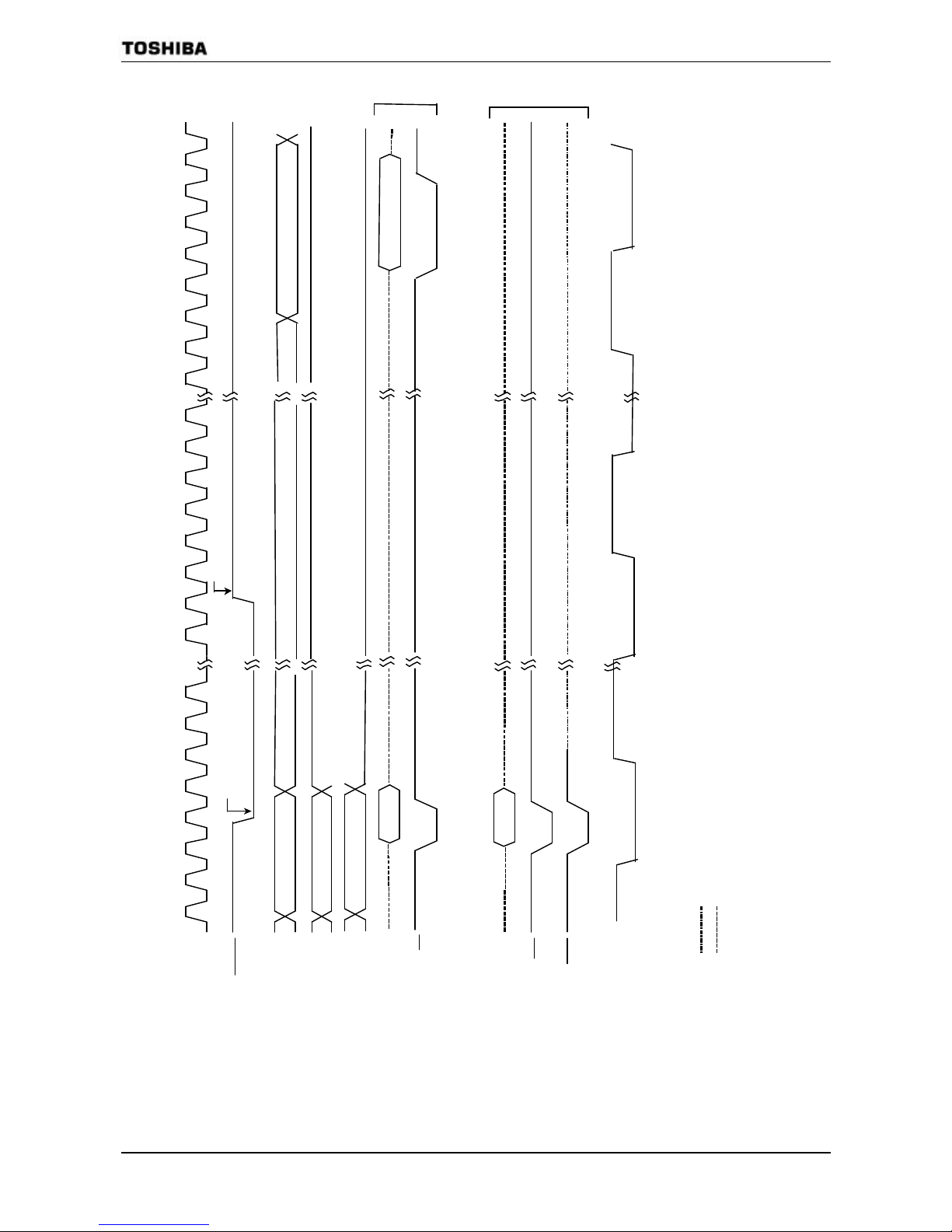
Figure 3.1.1 is a reset timing chart of the TMP91C824.
Page 13
TMP91C8 24
91C824-
10
readwrite
f
FPH
A23∼
0
DATA-IN
D0∼
15
D0
∼
15
sampling
(After reset released,,startting 2 wait read cycle)
Note
)
Pull-up (internal)
High-z
DATA-OUT
sampling
(P
52 input mode)
RESET
RD WR
HWR
/CS0,1, 3,
0FFFF00H
/CS
2
DATA-IN
XT1,XT2
Figure 3.1.1 TMP91C824 Reset Timing Chart
Page 14
TMP91C824
91C824-11
3.2 Memory Map
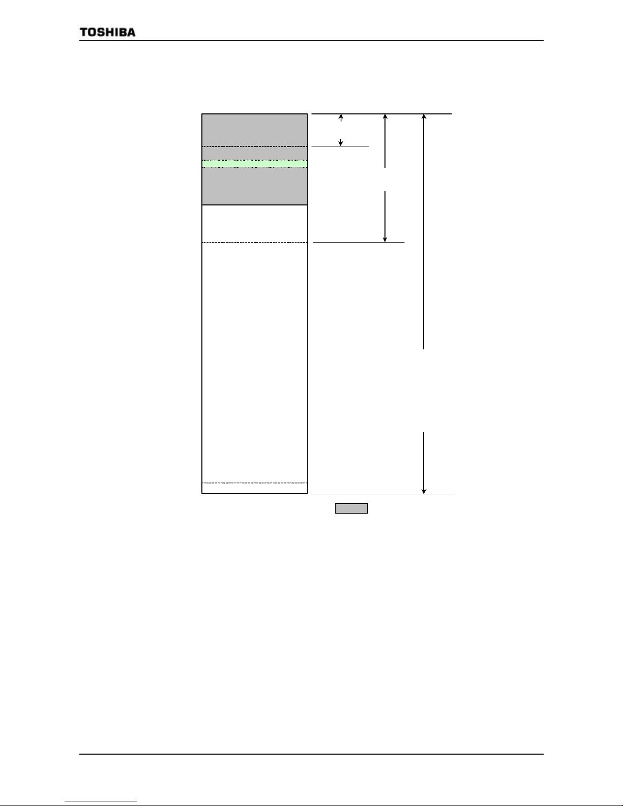
Figure 3.2.1 is a memory map of the TMP91C824.
000000H
001000H
16Mbyte area
(R)
(−R)
(R+)
(R + R8/16)
(R + d8/16)
(nnn)
Direct
area
(n)
64Kbyte area
(nn)
Internal I/O
(4KByte)
Internal RAM
(8K Byte)
003000H
010000H
(
=Internal area
)
FFFF00H
FFFFFFH
Vector table
(256 Byte)
External memory
000100H
000FE0H
Figure 3.2 1 Memory Map
Note : Address 000FE0H – 00FFFH is assigned for the TOSHIBA reserve area, user can’t use.
Page 15

TMP91C8 24
91C824-
12
3.3 Triple Clock Function and Standby Function
TMP91C824 contains (1) a clock gear, (2) clock doubler (DFM), (3) stand-by controller and (4)
noise-reduction circuit. It is used for low-power, low-noise systems.
This chapter is organized as follows:
3.3.1 Block diagram of system clock
3.3.2 SFRs
3.3.3 System clock controller
3.3.4 Prescaler clock controller
3.3.5 Clock doubler (DFM)
3.3.6 Noise-reducing circuit
3.3.7 Stand-by controller
Page 16
TMP91C824
91C824-
13
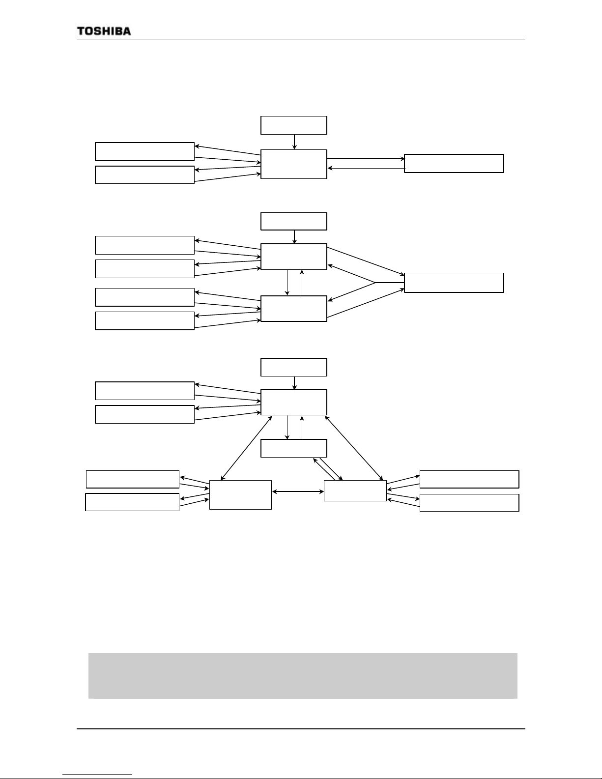
The clock operating modes are as follows: (a) Single Clock Mode (X1, X2 pins only), (b) Dual Clock Mode
(X1, X2, XT1 and XT2 pins) and (c) Triple Clock Mode (the X1, X2, XT1 and XT2 pins and DFM).
Figure 3.3.1 shows a transition figure.
Using DFM
instruction
Reset
(f
OSCH
/32)
release Reset
instruction
interrupt
STOP mode
(Stops all circuits)
NORMAL mode
(f
OSCH
/gear value/2)
IDLE2 mode
(I/O operate)
IDLE1 mode
(Operate only oscillator)
(a) Single clock mode transition figure
(b) Dual clock mode transition fiigure
STOP
mode
(Stops all circuits)
SLOW mode
(fs/2)
Reset
(f
OSCH
/32)
release Reset
NORMAL
mode
(f
OSCH
/gear value/2)
IDLE2
mode
(I/O operate)
IDLE1 mode
(Operate only oscillator)
IDLE2
mode
(I/O operate)
IDLE1 mode
(Operate only oscillator)
Reset
(f
OSCH
/32)
release Reset
NORMAL mode
(f
OSCH
/gear value/2)
IDLE2 mode
(I/O operate)
IDLE1 mode
(Operate only oscillator)
STOP mode
(Stops all circuits)
SLOW mode
(fs/2)
NORMAL mode
(4 × f
OSCH
/gear
value/2)
IDLE2 mode
(I/O operate)
IDLE1 mode
(Operate oscillator and
IDLE2 mode
(I/O operate )
IDLE1 mode
(Operate only oscillator)
(c) Triple clock mode trasision Figure
instruction
instruction
interrupt
interrupt
instruction
instruction
interrupt
interrupt
instruction
instruction
interrupt
interrupt
instruction
interrupt
instruction
instruction
interrupt
interrupt
instruction
instruction
instruction
interrupt
*NOTE
*NOTE)
・
It’s prohibited
to control DFM in SLOW mode when shifting from SLOW mode to NORMAL mode with use of
DFM.(DFM Start up/Stop/Change Write to DFMCR0<ACT1:0> resister)
・
If you shift from NORMAL mode with use of DFM to NORMAL mode,
the instruction should be separated into
two procedures as below. Change CPU clock ->Stop DFM circuit
・
It’s prohibited to shift from NORMAL mode with use of DFM to STOP mode directly. You should set
NORMAL
mode once, and then shift to STOP mode.(You should stop high frequency oscillator after you stop DFM.)
*NOTE
Figure 3.3.1 System clock block diagram
The clock frequency input from the X1 and X2 pins is called fc and the clock frequency input from the XT1 and XT2 pins is called fs. The
clock frequency selected by SYSCR1<SYSCK> is called the system clock f
FPH
. The system clock f
SYS
is defined as the div ided clock of
f
FPH
, and one cycle of f
SYS
is regred to as one state.
Page 17
TMP91C8 24
91C824-
14
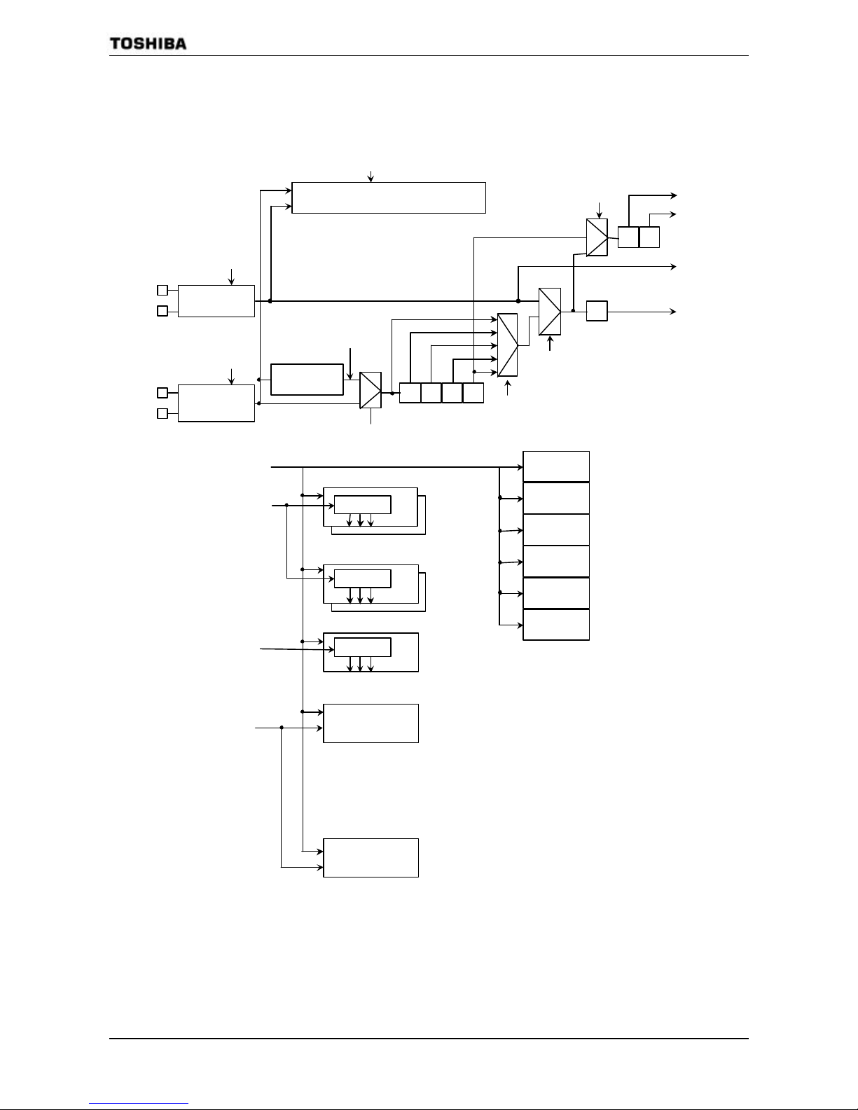
3.3.1 Block diagram of system clock
Clock gear
SYSCR1<SYSCK>
TMRA0 to 3
SYSCR0
<PRCK1, PRCK 0>
selector
fs
f
OSCH
Low-Frequency
oscillator
XT1
XT2
SYSCR0
<XTEN, RXTEN>
Warming up timer (High/Low frequency
oscillator), Lock up timer (DFM)
SYSCR0<WUEF>
SYSCR2<WUPTM1, WUPTM 0>
DFMCR0<ACT1, ACT 0, DLUPTM>
X1
X2
Clock Doubler
(DFM)
f
DFM
=
f
OSCH
×
4
÷
2
÷
16
÷
4
fc/16
fc/8
fc/4
fc/2
fc
DFMCR0<ACT1, ACT 0>
SYSCR1<GEAR2, GEAR 0>
÷2 ÷4
fc/16
f
FPH
f
SYS÷2
f
SYS CPU
RAM
ADC
Interrupt
controller
WDT
I/O ports
prescaler
φ
T0
SIO0 to1
SBI
RTC
φ
T
fs
φ
T0
fs
φ
T
SYSCR0
<XEN, RXTEN>
High-Frequency
oscillator
÷
8
prescaler
prescaler
MLD/ALM
Figure 3.3.2 Block Diagram of System clock
Page 18
TMP91C824
91C824-
15
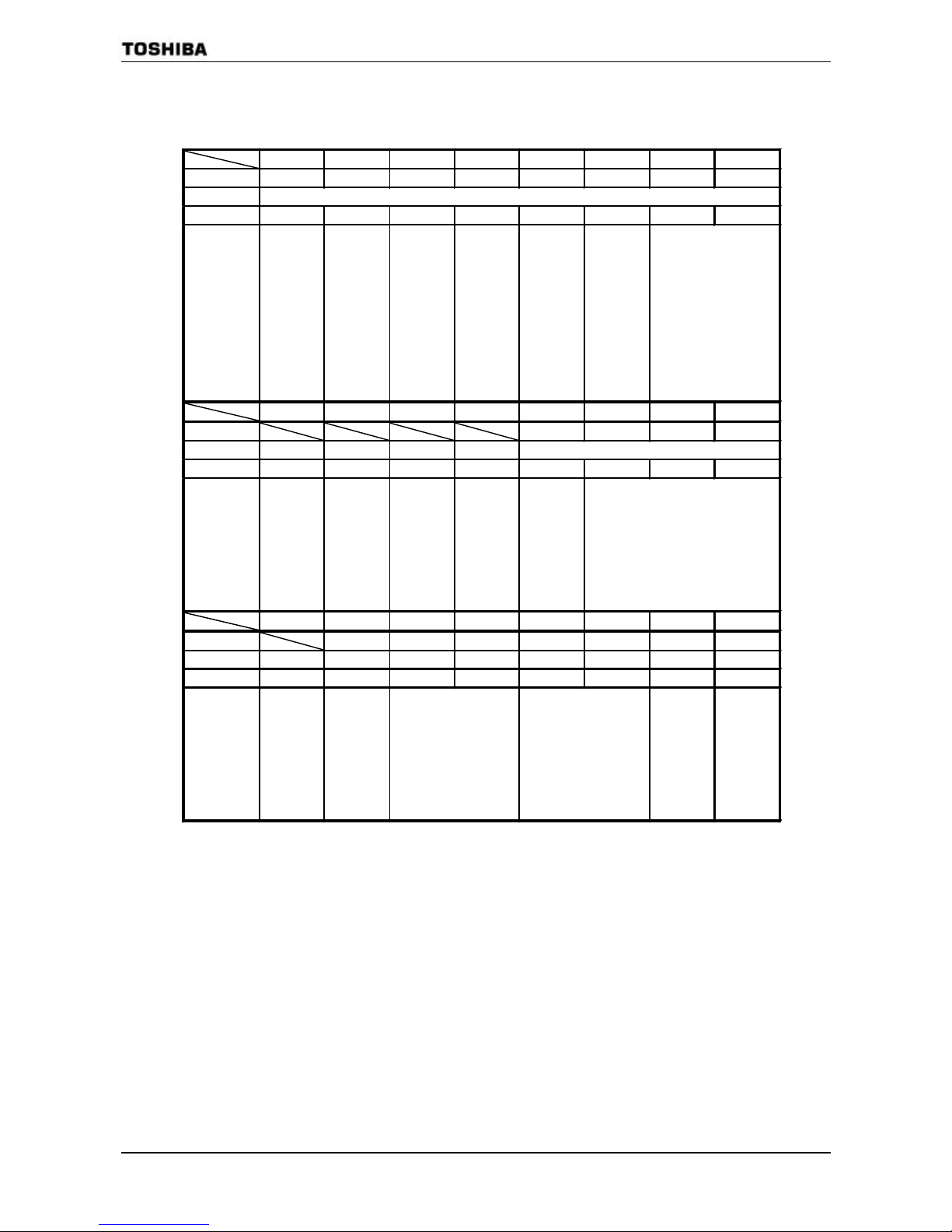
3.3.2 SFR
7 6 5 4 3 2 1 0
bit Symbol XEN XTEN RXEN RXTEN RSYSCK WUEF PRCK1 PRCK0
Read/Write
R/W
After reset 1 1 1 0 0 0 0 0
Function
High-frequen
cy oscillator
(fc)
0: Stop
1: Oscillation
Low-frequen
cy oscillator
(fs)
0: Stop
1: Oscillation
(note1)
High-frequen
cy oscillator
(fc) after
release of
Stop Mode
0: Stop
1: Oscillation
Low-frequen
cy oscillator
(fs) after
release of
Stop Mode
0: Stop
1: Oscillation
Selects clock
after release
of Stop
Mode
0: fc
1: fs
Warm-up
Timer
0: Write
Don’t care
1: Write
start timer
0: Read
end warm-up
1: Read
do not end
warm-up
Select prescaler clock
00: f
FPH (note2)
01: reserved
10: fc/16
11: reserved
7 6 5 4 3 2 1 0
bit Symbol SYSCK GEAR2 GEAR1 GEAR0
Read/Write
R/W
After reset 0 1 0 0
Function
Select
system clock
0: fc
1: fs
Select gear value of high frequency (fc)
000: fc
001: fc/2
010: fc/4
011: fc/8
100: fc/16
101: (reserved)
110: (reserved)
111: (reserved)
7 6 5 4 3 2 1 0
bit Symbol SCOSEL WUPTM1 WUPTM0 HALTM1 HALTM0 SELDRV DRVE
Read/Write
R/W R/W R/W R/W R/W R/W R/W
After reset 0 1 0 1 1 0 0
Function
0: fs
1: f
SYS
Warm-Up Timer
00: reserved
01: 28/inputted frequency
10:214
11:216
HALT mode
00: reserved
01: STOP mode
10: IDLE1 mode
11: IDLE2 mode
<DRVE>
mode
select
0: STOP
1: ID LE1
Pin state
control in
STOP/IDLE1
mode
0: I/O off
1: Remains
the state
before
HALT
SYSCR0
(00E0H)
SYSCR1
(00E1H)
SYSCR2
(00E2H)
(note1) By Reset, low-frequency oscillator is enable.
(note2) In case of using built-in SBI circuit, it must set SYSCR0<PRCK1:0> to ‘00’.
Figure 3.3.3 SFR for system clock
Page 19
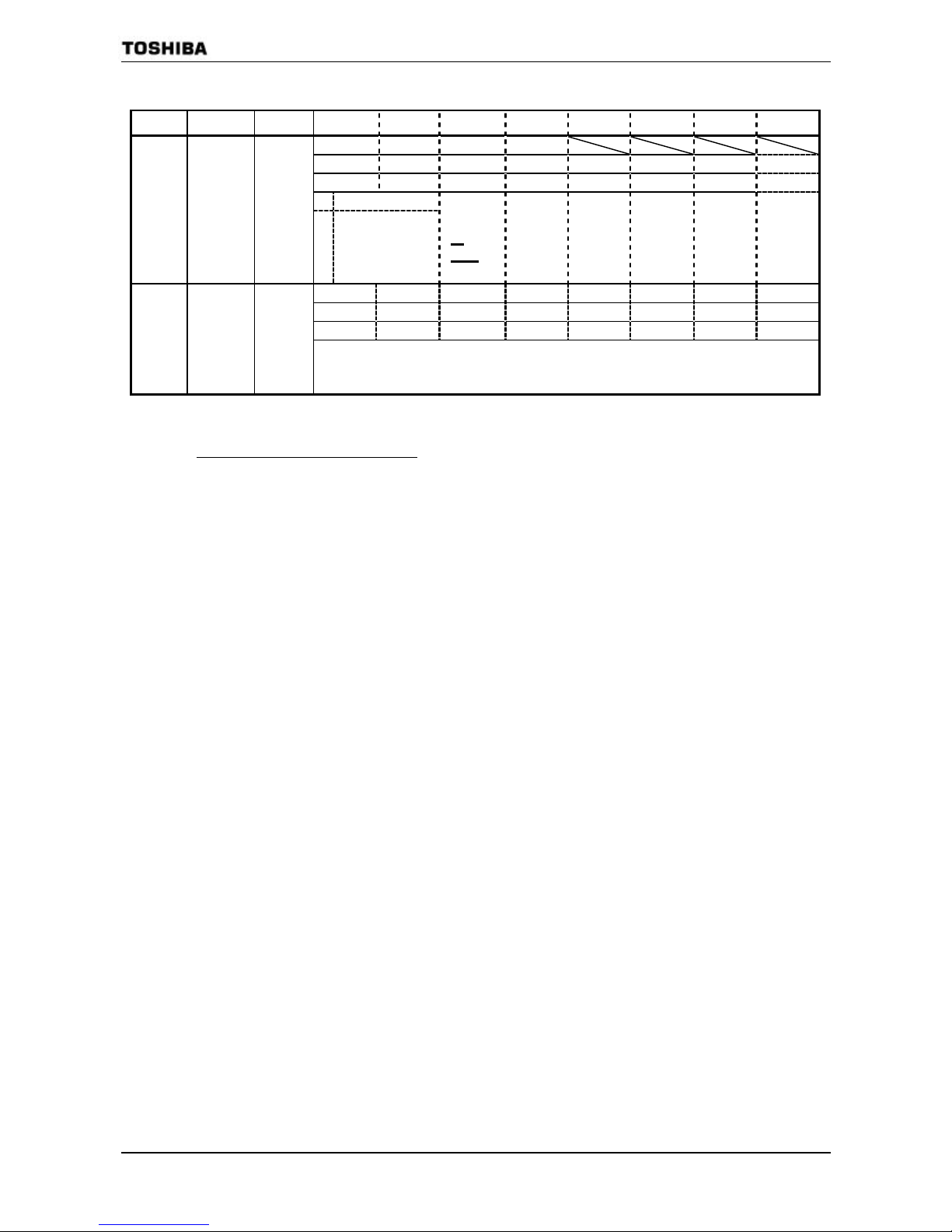
TMP91C8 24
91C824-
16
Figure 3.3.4 SFR for DFM
Symbol Name Address
7 6 5 4 3 2 1 0
ACT1 ACT0 DLUPFG DLUPTM
R/W R/W R R/W
0 0 0 0
DFM LUP
select f
FPH
DFMCR0
DFM
Control
Register 0
E8H
00
01
10
11
STOP
RUN
RUN
RUN
STOP
RUN
STOP
STOP
f
OSCH
f
OSCH
f
DFM
f
OSCH
Lock up
Status Flag
0: end
1: not end
Lock-up Time
0: 212/f
OSCH
1: 210/f
OSCH
R/W R/W R/W R/W R/W R/W R/W R/W
0 0 0 1 0 0 1 1
DFMCR1
DFM
Control
Register 1
E9H
DFM revision
Input frequency 4~6.75MHz(@2.7V~3.6V) : write “0BH”
Input frequency 2~2.5MHz(@2.0 ±10%) : write “1BH”
Limitation point on the use of DFM
1. It’ s prohibited to execute DFM enable/disable control in the SLOW mode(fs)
(write to DFMCR0 <ACT1:0>=”10”). You should control DFM in the NORMAL mode.
2. If you stop DFM operation during using DFM(DFMCR0<ACT1:0>=” 10”) , you shouldn’t execute that
change the clock f
DFM
to f
OSCH
and stop the DFM at the same time. Therefore the above executions sh ould be
separated into two procedures as showing below.
LD (DFMCR0),C0H ; change the clock f
DFM
to f
OSCH
LD (DFMCR0),00H ; DFM stop
3. If you stop high frequency oscillator during using DFM (DFMCR0<ACT1:0>= ”10”) , you should stop DFM
before you stop high frequency oscillator.
Please refer to 3.3.5 Clock Do ubler (DFM) for the details.
Page 20
TMP91C824
91C824-
17
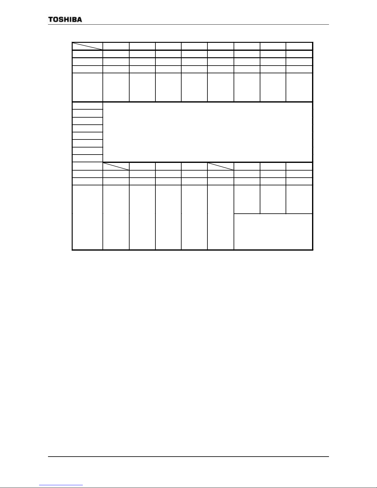
7 6 5 4 3 2 1 0
bit Symbol PROTECT TA3LCDE
– – – EXTIN DRVOSCH
DRVOSCL
Read/Write
R R/W R/W R/W R/W R/W R/W R/W
After reset 0 0 1 0 0 0 1 1
Function
Protect flag
0: OFF
1: ON
LCDC source
CLK
0: 32KHz
1: TA3OUT
Write “1” Write “0” Write “0” 1: Exte rnal
clock
fc oscillator
driver ability
1: NORMAL
0: WEAK
fs oscillator
driver ability
1: NORMAL
0: WEAK
bit Symbol
Read/Write
After reset
Function
bit Symbol
Read/Write
After reset
Function
Switching the protect ON/OFF by write to following 1st-KEY,2nd-KEY
1st-KEY: EMCCR1=5AH,EMCCR2=A5H in succession write
2nd-KEY: EMCCR1=A5H,EMCCR2=5AH in succession write
bit Symbol
ENFROM ENDROM ENPROM
FFLAG
DFLAG PFLAG
Read/Write
R/W R/W R/W R/W R/W R/W
After reset 0 0 0 0 0 0
CS1A write
Operation flag
CS2B-2G
write
operation
Flag
CS2A write
Operation
Flag
Function
CS1A area
detect control
0: disable
1: enable
CS2B-2G
area detect
control
0: disable
1: enable
CS2A area
detect control
0: disable
1: enable
When reading
“0” : not written
“1” : written
When writing
“0” : clear flag
EMCCR0
(00E3H)
EMCCR1
(00E4H)
EMCCR2
(00E5H)
EMCCR3
(00E6H)
(note) In case of Vcc=2V±10% use, fixed to EMCCR0<DRV0SCH>= ’1’.
Figure 3.3.5 SFR for noise-reduction
Page 21
TMP91C8 24
91C824-
18
3.3.3 System clock controller
The system clock controller generates the system clock signal (f
SYS
) for the CPU core and internal I/O.
It contains two oscillation circuits and a clock gear circuit for high-frequency (fc) operation. The register
SYSCR1<SYSCK> changes the system clock to either fc or fs, SYSCR0<XEN> and SYSCR0<XTEN>
control enabling and disabling of each oscillator, and SYSCR1<GEAR0 to GEAR2> sets the
high-frequency clock gear to either 1, 2, 4, 8 or 16 (fc, fc/2, fc/4, fc/8 or fc/16). These functions can
reduce the power consumption of the equipment in which the device is installed.
The combination of settings <XEN> = 1, <XTEN> = 0, <SYSCK> = 0 and <GEAR0~GEAR2> = 100
will cause the system clock (f
SYS
) to be set to fc/32 (fc/16 ×1/2) after a Reset.
For example, f
SYS
is set to 0.5 MHz when the 16-MHz oscillator is connected to the X1 and X2 pins.
(1) Switching from Normal Mode to Slow Mode
When the resonator is connected to the X1 and X2 pins, or to the XT1 and XT2 pins, the warm -up
timer can be used to change the operation frequency after stable oscillation has been attained.
The warm -up time can be selected using SYSCR2<WUPTM0,WUPTM1>.
This warm -up timer can be programmed to start and stop as shown in the following examples 1
and 2.
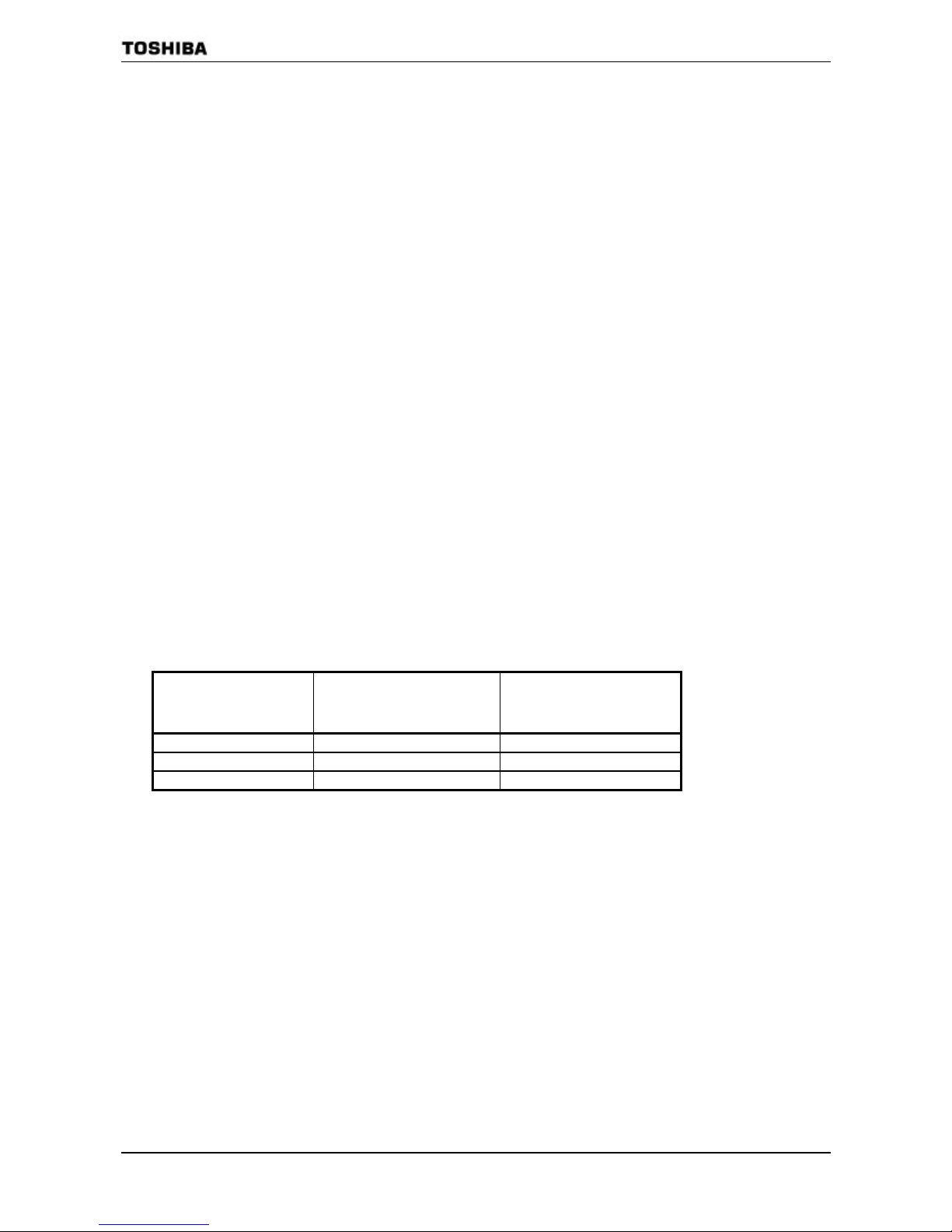
Table 3.3.1 shows the warm-up time.
Note 1: When using an oscillator (other than a resonator) with stable oscillation, a warm-up timer is
not needed.
Note 2: The warm -up timer is operated by an oscillation clock. Hence, there may be some variation
in warm -up time.
Table 3.3.1 Warming-up times
Warming-up Time
SYSCR2
<WUPTM1,WUPTM0>
Change to
Normal Mode
Change to
Slow Mode
01 (28 / frequency) 16 (µs) 7.8 (ms)
10 (214 / frequency) 1.024 (ms) 500 (ms)
11 (216 / frequency) 4.096 (ms) 2000 (ms)
at f
OSCH
= 16 MHz,
fs = 32.768 kHz
Page 22
TMP91C824
91C824-
19
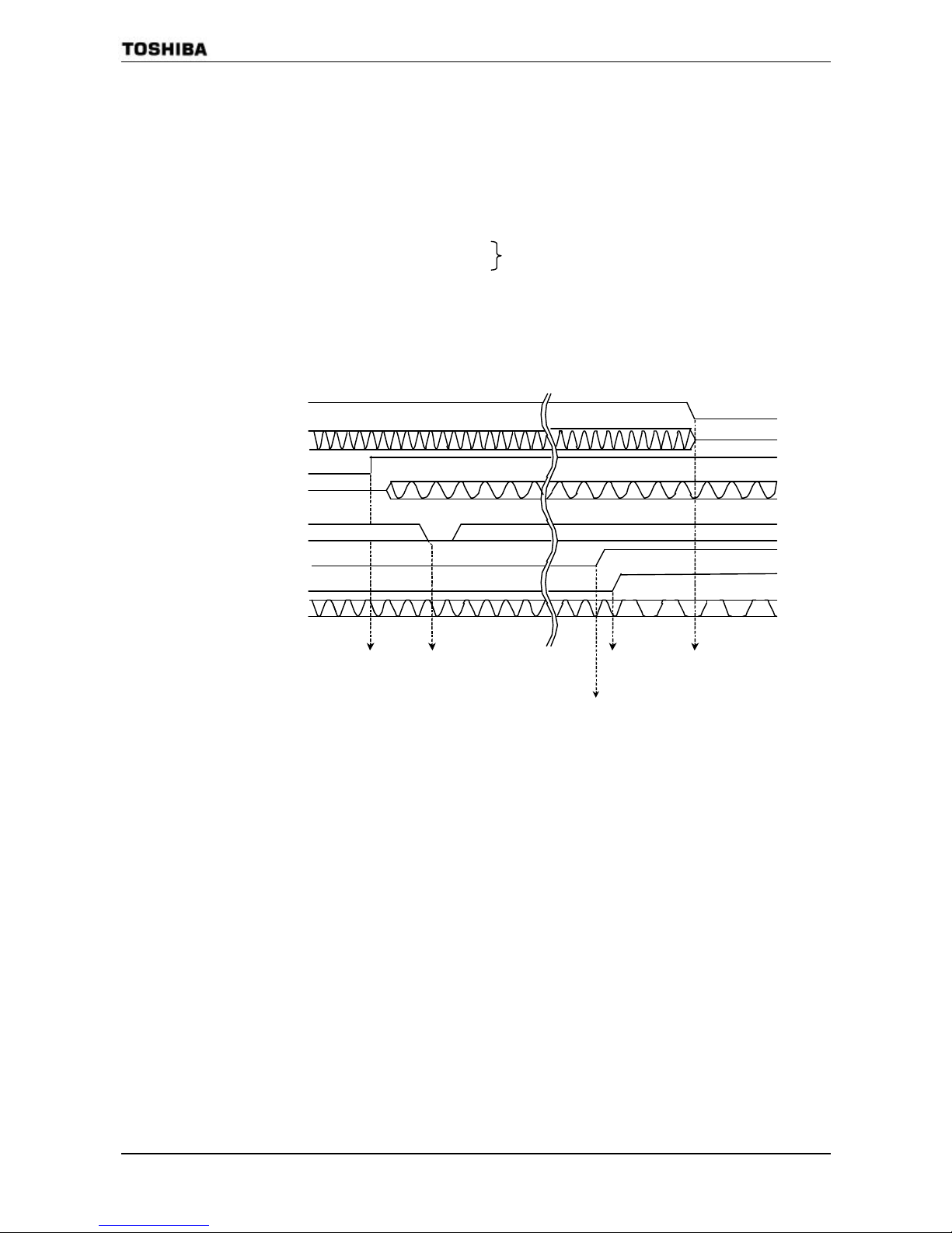
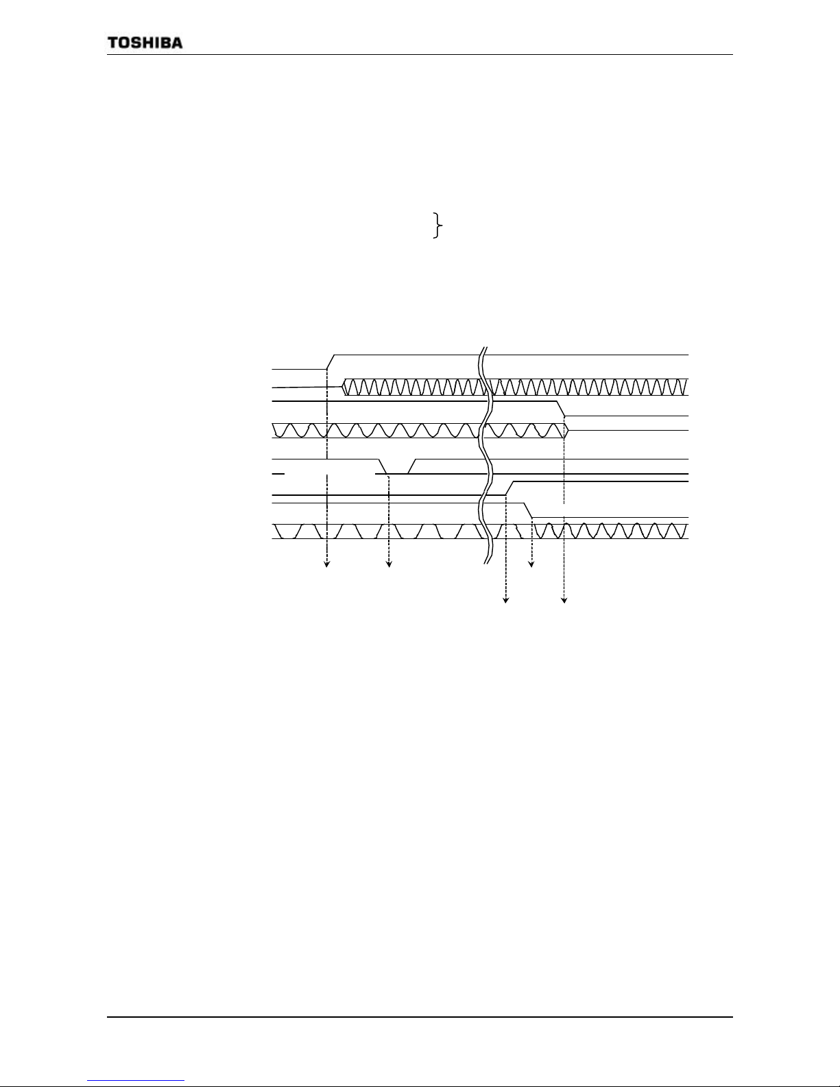
Example 1-Setting the clock
Changing from high frequency (fc) to low frequency (fs).
SYSCR0 EQU 00E0H
SYSCR1 EQU 00E1H
SYSCR2 EQU 00E2H
LD (SYSCR2), X−11− −X−B ; Sets warm-up time to 216/fs.
SET 6, (SYSCR0) ; Enables low-frequency oscillation.
SET 2, (SYSCR0) ; Clears and starts warm-up timer.
WUP: BIT 2, (SYSCR0) ;
JR NZ, WUP ;
Detects stopping of warm-up timer.
SET 3, (SYSCR1) ;
Changes f
SYS
from fc to fs.
RES 7, (SYSCR0) ; Disables high-frequency oscillation.
(note) “ x” means don’t care
“-“ means no change
fc
fs
Counts up by fs
<XEN>
X1, X2 pins
XT1, XT2 pins
<XTEN>
Warming Up Timer
End of Warming Up Timer
<SYSCK>
System Clock f
SYS
Enables
low Frequency
Clears and starts
warming-up timer
End of warming up timer
Chages fsys
from fc to fs
Disabiles
high-frequency
Counts up by f
SYS
Page 23
TMP91C8 24
91C824-
20
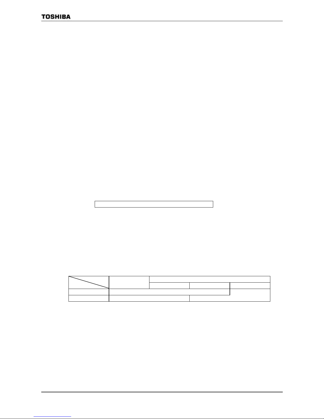
Example 2-Setting the clock
Changing from low frequency (fs) to high frequency (fc).
SYSCR0 EQU 00E0H
SYSCR1 EQU 00E1H
SYSCR2 EQU 00E2H
LD (SYSCR2), X−10− −X−B ; Sets warm-up time to 214/fc.
SET 7, (SYSCR0) ; Enables high-frequency oscillation.
SET 2, (SYSCR0) ; Clears and starts warm-up timer.
WUP: BIT 2, (SYSCR0) ;
JR NZ, WUP ;
Detects stopping of warm-up timer.
RES 3, (SYSCR1) ; Changes f
SYS
from fs to fc.
RES 6, (SYSCR0) ; Disables low-frequency oscillation.
(note) “ x” means don’t care
“-“ means no change
Counts up by fc
<XEN>
X1, X2 pins
XT1, XT2 pins
<XTEN>
Warming Up Timer
End of Warming Up Timer
<SYSCK>
System Clock f
SYS
Enables
High Frequency
Clears and Starts
Warming Up Timer
End of warming
up timer
Chages fsys
from fs to fc
Disables
low-frequency
fc
Counts up by f
SYS
fs
Page 24
TMP91C824
91C824-
21
(2) Clock gear controller
When the high-frequency clock fc is selected by setting SYSCR1<SYSCK> = 0, f
FPH
is set
according to the contents of the Clock Gear Select Register SYSCR1<GEAR0 to GEAR2> to either
fc, fc/2, fc/4, fc/8 or fc/16. Using the clock gear to select a lower value of f
FPH
reduces power
consumption.
Example 3
Changing to a high-frequency gear
SYSCR1 EQU 00E1H
LD (SYSCR1), XXXX0000B ;
Changes f
SYS
to fc/2.
LD (SYSCR1), XXXX0100B ;
Changes f
SYS
to fc/32.
X: Don't care
(High-speed clock gear changing)
To change the clock gear, write the register value to the SYSCR1<GEAR2-0> register.It is necessary the
warmming up time until changing after writing the register value.
There is the possibility that the instructio n next to the clock gear changing instruction is executed by the
clock gear before changing.To execute the instruction next to the clock gear switching instruction by the clock
gear after changing,input the dummy instruction as follows (instruction to execute the write cycle).
(Example)
SYSCR1 EQU 00E1H
LD (SYSCR1), XXXX0001B ;
Changes f
SYS
to fc/4.
LD (DUMMY), 00H ; Dummy instruction
Instruction to be executed after clock gear has changed
(3) Internal clock terminal out function
It can out internal clock(f
SYS
or fS) from PD5/SCOUT.
PD5 pin function is set to SCOUT output by the following bit setting.
: PDFC<PD5F>= ’1’
Output clock select
:Refer to SYSCR2<SCOSEL> bit setting
HALT mode HALT mode
SCOUT select
NORMAL
SLOW
IDLE2 IDEL1 STOP
<SCOSEL>=’0’ fS clock out
<SCOSEL>=’1’ f
SYS
clock out ‘0’ or ‘1’ fix out
Page 25
TMP91C8 24
91C824-
22
3.3.4 Prescaler clock controller
For the internal I/O (TMRA01 to 23, SIO0 to 1) there is a prescaler which can divide the clock.
The φT 0 clock input to the prescaler is either the clock f
FPH
divided by 4 or the clock fc/16 divided by
4. The setting of the SYSCR0 <PRCK0 to PRCK1> register determines which clock signal is input.
3.3.5 Clock doubler (DFM)
DFM outputs the f
DFM
clock signal, which is four times as fast as f
OSCH
. It can use the low-frequency
oscillator, even though the internal clock is high-frequency.
A Reset initializes DFM to Stop status, setting to DFMCR0 -register is needed before use.
Like an oscillator, this circuit requires time to stabilize. This is call ed the lock-up time.
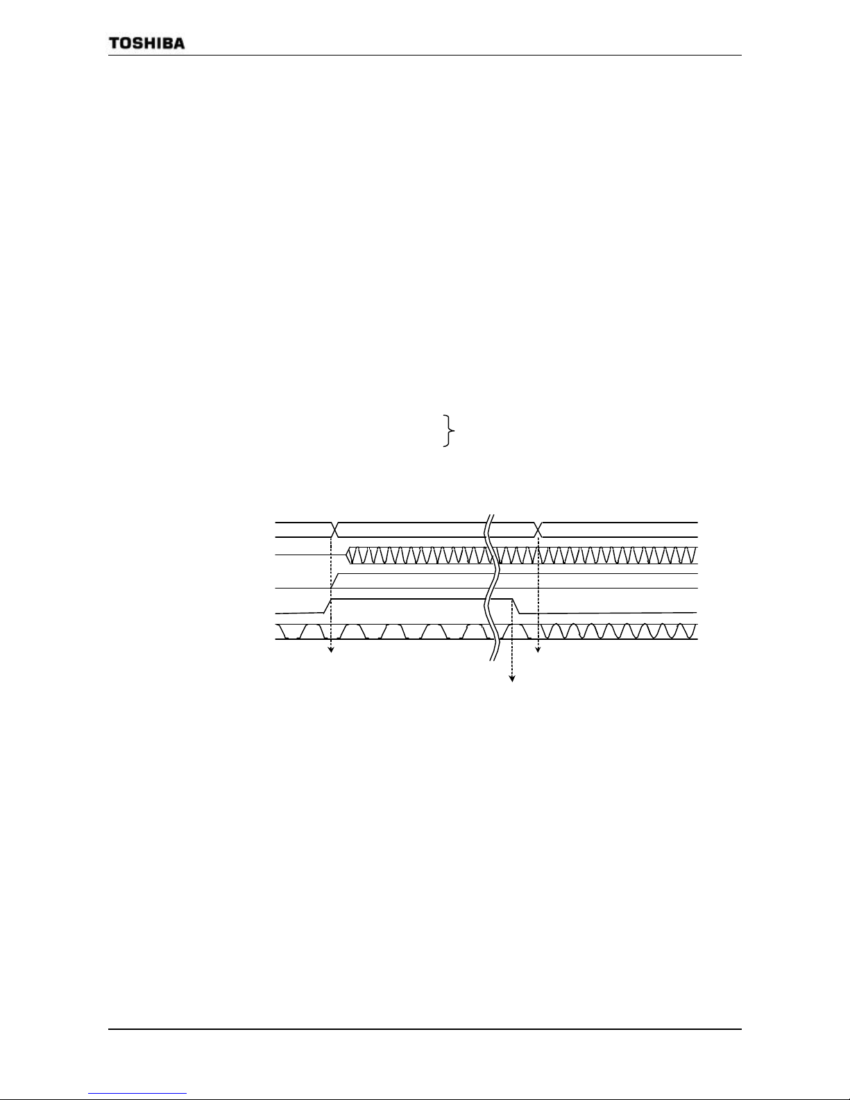
The following example shows how DFM is used.
DFMCR0 EQU 00E8H
DFMCR1 EQU 00E9H
LD (DFMCR1),00001011B
DFM parameter setting
LD (DFMCR0), 01X0XXXXB ; Set lock-up time to 212/4 MHz
Enables DFM operation and starts lock-up.
LUP: BIT 5, (DFMCR0) ;
JR NZ, LUP ;
Detects end of lock -up
LD (DFMCR0), 10X0XXXXB ; Changes fc from 4 MHz to 16 MHz.
X: Don't care
1001
Counts up by f
OSCH
During lock-up
ACT1:0
DFM output: f
DFM
Lockup timer
<DLUPFG>
System clock f
SYS
Starts DFM operation.
Starts lock-up.
Ends of lock-up
Changes from 4 MHz to 16 MHz.
After lock-up
(note) Input frequency limitation and correction for DFM
Recommend to use Input frequency(High speed oscillation) for DFM in the following condition.
f
OSCH
= 4 ~ 6.75MHz (Vcc = 2.7~ 3.6V) : write 0BH to DFMCR1
f
OSCH
= 2 ~ 2.5MHz (Vcc = 2.0V ±10%) : write 1BH to DFMCR1
Page 26

TMP91C824
91C824-
23
Limitation point on the use of DFM
1. It’ s prohibited to execute DFM enable/disable control in the SLOW mode(fs)
(write to DFMCR0<ACT1:0>=”10”). You should control DFM in the NORMAL mode.
2. If you stop DFM operation during using DFM (DFMCR0<ACT1:0>=” 10”) , you shouldn’t execute the
commands that change the clock f
DFM
to f
OSCH
and stop the DFM at the same time. Therefore the above
execution should be separated into two procedures as showing below.
LD (DFMCR0),C0H ; Change the clock f
DFM
to f
OSCH
LD (DFMCR0),00H ; DFM stop
3. If you stop high frequency oscillator during using DFM(DFMCR0<ACT1:0>= ”10”) , you should stop DFM
before you stop high frequency oscillator.
Examples of settings are below.
(1) Start Up / Change Control
(OK) Low frequency oscillator operation mode(fs) (high frequency oscillator STOP)
→ High frequency oscillator start up → High frequency oscillator operation mode(f
OSCH
)→DFM
start up → DFM use mode (f
DFM
)
LD (SYSCR0), 11---1--B ; High frequency oscillator start up/ Warming up start
WUP: BIT 2,(SYSCR0) ;
JR NZ,WUP ;
LD (SYSCR1), ----0---B ; Change the system clock fs to f
OSCH
LD (DFMCR0),01-0----B ; DFM start up / lock up start
LUP: BIT 5, (DFMCR0) ;
JR NZ,LUP ;
LD (DFMCR0),10-0----B ; Change the system clock f
OSCH to fDFM
(OK) Low frequency oscillator operation mode(fs) (high frequency oscillator Operate)
→ High frequency oscillator operation mode(f
OSCH
)→DFM start up → DFM use mode (f
DFM
)
LD (SYSCR1), ----0---B ; Change the system clock fs to f
OSCH
LD (DFMCR0), 01 -0----B ; DFM start up / lock up start
LUP: BIT 5, (DFMCR0) ;
JR NZ,LUP ;
LD (DFMCR0),10-0----B ; Change the system clock f
OSCH to fDFM
(NG) Low frequency oscillator operation mode(fs) (high frequency oscillator STOP)
→ High frequency oscillator start up → DFM start up → DFM use mode (f
DFM
)
LD (SYSCR0),11---1--B ; High frequency oscillator start up/ Warming up start
WUP: BIT 2,(SYSCR0) ;
JR NZ,WUP ;
LD (DFMCR0),01-0----B ; DFM start up / lock up start
LUP: BIT 5, (DFMCR0) ;
JR NZ,LUP ;
LD (DFMCR0),10-0----B ; Change the internal clock f
OSCH to fDFM
LD (SYSCR1), -----0---B ; Change the system clock fs to f
DFM
Check for the flag of warming up end
Check for the flag of warming up end
Check for the flag of lock up end
Check for the flag of lock up end
Check for the flag of lock up end
Page 27

TMP91C8 24
91C824-
24
(2)Change / Stop Control
(OK) DFM use mode (f
DFM
)→ High frequency oscillator operation mode(f
OSCH
)→ DFM Stop
→ Low frequency oscillator operation mode(fs)→High frequency oscillator stop
LD (DFMCR0),11------B ; Change the system clock f
DFM
to f
OSCH
LD (DFMCR0),00------B ; DFM stop
LD (SYSCR1), ----1---B ; Change the system clock f
OSCH
to fs
LD (SYSCR0), 0 -------B ; High frequency oscillator stop
(NG) DFM use mode (f
DFM
)→ Low frequency oscillator operation mode(fs)→ DFM stop
→High frequency oscillator stop
LD (SYSCR1), ----1---B ; Change the system clock f
DFM
to fS
LD (DFMCR0),11------B ; Change the internal clock (fC) f
DFM to fOSCH
LD (DFMCR0),00------B ; DFM stop
LD (SYSCR0), 0 -------B ; High frequency oscillator stop
(OK) DFM use mode (f
DFM
)→Set the STOP mode
→High frequency oscillator operation mode (f
OSCH
)→ DFM stop→ HALT(High frequency
oscillator stop)
LD (SYSCR2), ----01--B ; Set the STOP mode
(This command can execute before use of DFM)
LD (DFMCR0),11------B ; Change the system clock f
DFM
to f
OSCH
LD (DFMCR0),00------B ; DFM stop
HALT ; Shift to STOP mode
(NG) DFM use mode (f
DFM
)→Set the STOP mode→ HALT(High frequency oscillator stop)
LD (SYSCR2), ----01--B ; Set the STOP mode
(This command can execute before use of DFM)
HALT ; Shift to STOP mode
Page 28
TMP91C824
91C824-
25
Noise reduction circuits
Noise reduction circuits are built in, allowing implementation of the following features.
(1) Reduced drivability for high-frequency oscillator
(2) Reduced drivability for low-frequency oscillator
(3) Single drive for high-frequency oscillator
(4) SFR protection of register contents
(5) ROM protection of register contents
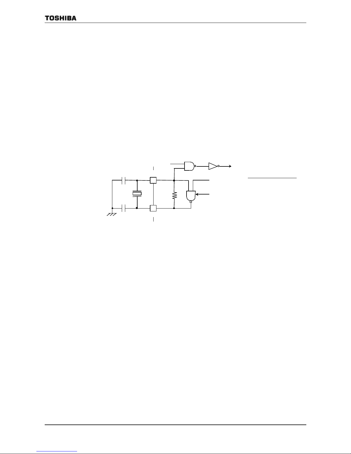
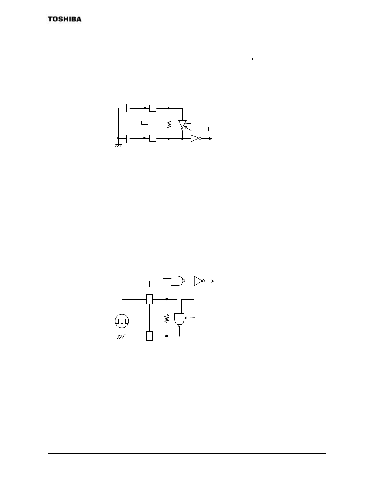
(1) Reduced drivability for high-frequency oscillator
(Purpose)
Reduces noise and power for oscillator when a resonator is used.
(Block diagram )
resonator
C2 C1
Enable oscillation
X1 pin
EMCCR0<DRVOSCH>
f
OSCH
(STOP+EMCCR0<EXTIN>)
X2 pin
(Setting method)
The drivability of the oscillator is reduced by writing”0” to EMCCR0<DRVOSCH> register. By
reset, <DRVOSCH> is initialized to “1” and the oscillator starts oscillation by normal-drivability
when the power -supply is on.
Don’t set <DRVOSCH> to “0” at Vcc=2V±10%.
Page 29
TMP91C8 24
91C824-
26
(2) Reduced drivability for low-frequency oscillator
(Purpose)
Reduces noise and power for oscillator when a resonator is used.
(Block diagram )
X
T1 pin
Resonato
C2
C1
Enable oscillation
EMCCR0<DRVOSCL>
f
S
XT2
pin
(Setting method)
The drivability of the oscillator is reduced by writing 0 to the EMCCR0<DRVOSCL> register.
By Reset, <DRVOSCL> is initialized to “1”.
(3) Single drive for high-frequency oscillator
(Purpose)
Not need twin-drive and protect mistake-operation by inputted noise to X2 pin when the
external-oscillator is used.
(Block diagram )
X1 pin
X2 pin
Enable oscillation (STOP+EMCCR0<EXTIN>)
EMCCR0<DRVOSCH>
f
OSCH
(Setting method)
The oscillator is disabled and starts operation as buffer by writing “ 1” to EMCCR0<EXTIN>
register.X2-pin is always outputted”1”.
By reset, <EXTIN> is initialized to “0”.
Page 30

TMP91C824
91C824-
27
(4) Runaway provision with SFR protection register
(Purpose)
Provision in runaway of program by noise mixing.
Write operation to specified SFR is prohibited so that provision program in runaway prevents that
it is it in the state which is fetch impossibility by stopping of clock, memory control register
(CS/WAIT controller, MMU) is changed.
And error handling in runaway becomes easy by INTP0 interruption.
Specified SFR list
1. CS/WAIT controller
B0CS, B1CS, B2CS, B3CS, BEXCS,
MSAR0, MSAR1, MSAR2, MSAR3,
MAMR0, MAMR1, MAMR2, MAMR3
2. MMU
LOCAL0/1/2/3
3. Clock gear
SYSCR0, SYSCR1, SYSCR2, EMCCR0,EMCCR3
4. DFM
DFMCR0, DFMCR1
(Operation explanation)
Execute and release of protection (write operation to specified SFR) become possible by setting
up a double key to EMCCR1 and EMCCR2 register.
(Double key)
1st-KEY : Succession writes in 5AH at EMCCR1 and A5H at EMCCR2
2nd-KEY : Succession writes in A5H at EMCCR1 and 5AH at EMCCR2
A state of protection can be confirmed by reading EMCCR0<PROTECT>.
By reset, protection becomes OFF.
And INTP0 interruption occurs when write operation to specified SFR was executed with
protection ON state.
Page 31

TMP91C8 24
91C824-
28
(5) Runaway provision with ROM protection register
(Purpose)
Provision in runaway of program by noise mixing.
(Operation explanation)
When write operation was executed for external three kinds of ROM by runaway of program,
INTP1 is occurred and detects runaway function.
Three kinds of ROM is fixed as for Flash-ROM(Option-Program ROM), Data-ROM,
Program-ROM are as follows on the logical address memory map.
1. Flash-ROM : Address 400000H-7FFFFFH
2. Data-ROM : Address 800000H-BFFFFFH
3. Program-ROM : Address C00000H -FFFFFFH
For these address, admission / prohibition of detection of write operation sets it up with
EMCCR3<ENFROM,ENDROM,ENPROM>. And INTP1 interruption occurred within which
ROM can confirm each with EMCCR3<FFLAG,DFLAG,PFLAG>. This flag is cleared when write
in "0".
Page 32
TMP91C824
91C824-
29
3.3.6 Standby controller
(1) Halt Modes
When the HALT instruction is executed, the operating mode switches to Idle2, Idle1 or Stop
Mode, depending on the contents of the SYSCR2<HALTM1,HALTM0> register.
The subsequent actions performed in each mode are as follows:
• IDLE2: Only the CPU halts.
The internal I/O is available to select operation during IDLE2 mode.by setting the
following register.
Table 3.3 2 Shows the registers of setting operation during IDLE2 m ode.
Table 3.3.2 SFR seting operation during IDLE2 mode
Internal I/O SFR
TMRA01 TA01RUN<I2TA01>
TMRA23 TA23RUN<I2TA23>
SIO0 SC0MOD1<I2S0>
SIO1 SC1MOD1<I2S1>
A/D converter ADMOD1<I2AD>
WDT WDMOD<I2WDT>
SBI SBI0BR0<I2SBI0>
‚ Idle1: Only the oscillator and the RTC (real-time clock) continue to operate.
ƒ Stop: All internal circuits stop operating.
The operation of each of the different Halt Modes is described in Table 3.3.3.
Table 3.3.3 I/O operation during Halt Modes
Halt Mode IDLE2 IDLE1 STOP
SYSCR2 <HALTM1:0> 11 10 01
CPU Stop
I/O ports Keep the state when the HALT instruction
was executed.
See table 3.3.6
TMRA
SIO, SBI
A/D converter
WDT
S top
Block
RTC,MLD
Available to select
operation block
Possible to operate
Page 33

TMP91C8 24
91C824-
30
(2) How to release the Halt mode
These HALT states can be released by resetting or requesting an interrupt. The halt release
sources are determined by the combination between the states of interrupt mask register <IFF2-0>
and the halt modes. The details for releasing the HALT status are shown in Table 3.3 4.
• Released by request ing an interrupt
The operating released from the halt mode depends on the interrupt enabled status.When the
interrupt request level set before executing the HALT instruction exceeds the value of interrupt
mask register,the interrupt due to the source is processed after releasing the halt mode,and CPU
status executing an instruction that follows the HALT instruction. When the interrupt request level
set before executing the HALT instruction is less than the value of the interrupt mask
register,releasing the halt mode is not executed.(in non-maskable interrupts,interrupt processing is
processed after releasing the halt mode regardless of the value of the mask register.) However only
for INT0~INT4 and RTC interrupts,even if the interrupt request level set before executing the
HALT instruction is less than the value of the interrupt m ask register, releasing the the halt mode is
executed. In this case,interrupt process ing, and CPU starts executing the instruction next to the
HALT instruction,but the interrupt request flag is held at “1”.
(Note) Usually, interrupts can release all halts status. However, the interrupts
(/NMI,INT0-3,INTKEY,INTRTC,INTALM0 to 4) which can release the HALT mode may not be
able to do so if they are input during the period CPU is shifting to the HALT mode(for about 5 clocks
of f
FPH
) with IDLE1 or STOP mode(IDLE2 is not applicable).(In this case,an interrupt request is kept
on hold internally)
If another interrupt is generated after it has shifted to HALT mode completely, halt status can be
released without difficulty.The priority of this interrupt is compared with that of the interrupt kept on
hold internally,and the interrupt with higher priority is handled first followed by the other interrupt.
• Releasing by resetting
Releasing all halt status is executed by resetting.
When the Stop m ode is released by RESET,it is necessry enough resetting time (see table 3.3.5)
to set the operation of the oscillator to be stable.
When releasing the halt mode by resetting, the internal RAM data keeps the state before the
“HALT” instruction is executed. However the other settings contents are initialized. (Releasing due
to interrupts keeps the state before the “HALT” instruction is executed.)
Page 34
TMP91C824
91C824-
31
Table 3.3.4 Source of Halt state clearance and Halt clearance operation
Status of Received Interrupt
Interrupt Enabled
(interrupt level) ≥ (interrupt mask)
Interrupt Disabled
(interrupt level) < (interrupt mask)
Halt mode Idle2 Idle1 Stop
Idle2 Idle1 Stop
Interrupt
NMI
INTWDT
INT0 ? ? ?3 (Note1)
INTALM0 to 4
INTTA0 to 3
INTRX0 to 1,TX0 to 1
INTAD
INTKEY
INTRTC
INTSBI
¥
¥
¥
¥
¥
¥
¥
¥
¥
¥
¥
×
¥
¥
×
×
×
¥
¥
×
¥
*1
×
¥
*1
×
×
×
×
¥
*1
×
×
−
−
¡
¡
×
×
×
¡
¡
×
−
−
¡
¡
×
×
×
¡
¡
×
−
−
¡
*1
×
×
×
×
¡
*1
×
×
Source of Halt state clearance
RESET
¥ ¥ ¥ ¥ ¥ ¥
¥: After clearing the Halt mode, CPU starts interrupt processing. (RESET initializes the microcont.)
¡: After clearing the Halt mode, CPU resumes executing starting from instruction following the HALT instruction.
×: It can not be used to release the halt mode.
−: The priority level (interrupt request level) of non-maskable interrupts is fixed to 7, the highest priority level. There
is not this combination type.
*1: Releasing t he halt mode is executed after passing the warmming-up time.
Note 1: When the Halt mode is cleared by an INT0 interrupt of the level mode in the interrupt enabled status, hold
level H until starting interrupt processing. If level L is set before holding level L, interrupt processing is
correctly started.
(Example - clearing Idle1 Mode)
An INT0 interru pt clears the Halt state when the device is in Idle1 Mode.
Address
8203H LD (IIMC), 00H ; Selects INT0 interrupt rising edge.
8206H LD (INTE0AD), 06H ; Sets INT0 interrupt level to 6.
8209H EI 5 ; Sets interrupt level to 5 for CPU.
820BH LD (SYSCR2), 28H ; Sets Halt mode to Idle1 Mode.
820EH
HALT
; Halts CPU.
INT0 INT0 interrupt routine
RETI
820FH LD XX, XX
Page 35
TMP91C8 24
91C824-
32
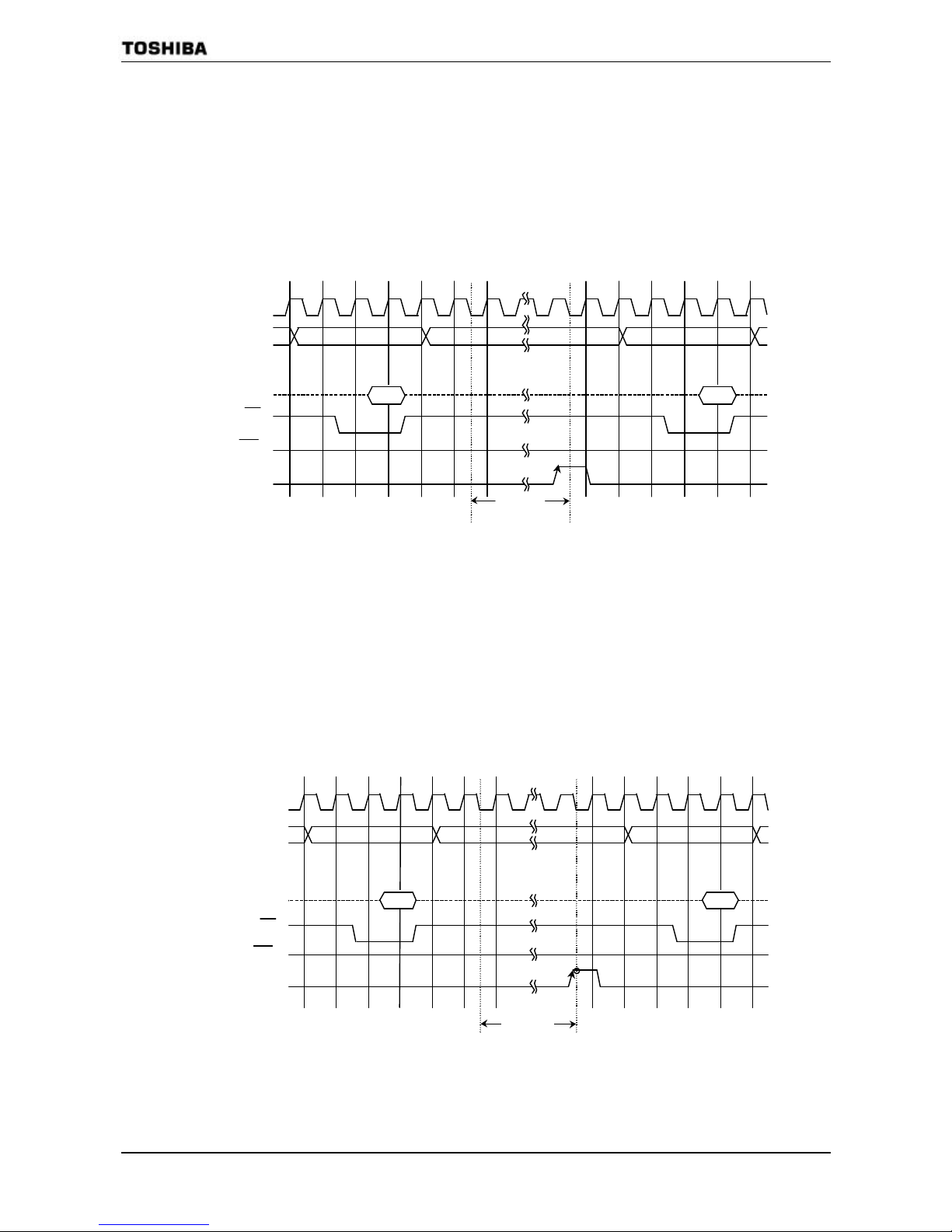
(3) Operation
① IDLE2 Mode
In Idle2 Mode only specific internal I/O operations, as designated by the Idle2 Setting Register,
can take place. Instruction execution by the CPU stops.
Figure 3.3 6 illustrates an example of the timing for clearance of the Idle2 Mode Halt state by an
interrupt.
N e x t N e x t + 2
X1
A0 ∼ 23
RD
WR
D0 ∼ 15
Data Data
IDLE2
mode
Interrupt for
release
Figure 3.3.6 Timing chart for Idle2 Mode Halt state cleared by interrupt
② Idle1 Mode
In Idle1 Mode, only the internal oscillator and the RTC,MLD continue to operate. The system
clock in the MCU stops. The pin status in the IDLE1 mode is depended on setting the register
SYSCR2<SELDRV,DRVE>. Table 3.3 6 summarizes the state of these pins in the IDLE mode1.
In the Halt state, the interrupt request is sampled asynchronously with the system clock; however,
clearance of the Halt state (i.e. restart of operation) is synchronous with it.
Figure 3.3 7 illustrates the timing for clearance of the Idle1 Mode Halt state by an interrupt.
N e x t N e x t + 2
X1
A0 ∼ 23
RD
WR
Interrupt
for release
IDLE1 mode
D0 ∼ 15
Data Data
Figure 3.3.7 Timing chart for Idle1 Mode Halt state cleared by interrup
Page 36
TMP91C824
91C824-
33
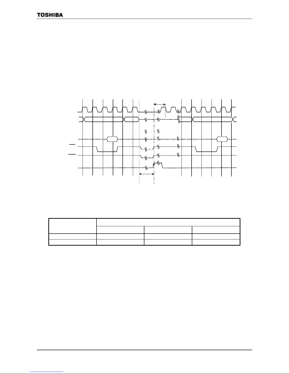
③ Stop Mode
When Stop Mode is selected, all internal circuits stop, including the internal oscillator Pin status
in Stop Mode depends on the settings in the SYSCR2<DRVE> register. Table 3.3.6 summarizes the
state of these pins in Stop Mode.
After Stop Mode has been cleared system clock output starts when the warm -up time has elapsed,
in order to allow oscillation to stabilize. After Stop Mode has been cleared, either Normal Mode or
Slow Mode can be selected using the SYSCR0<RSYSCK> register. Therefore, <RSYSCK>,
<RXEN> and <RXTEN> must be set See the sample warm -up times in Table 3.3.5.
Figure 3.3.8 illustrates the timing for clearance of the Stop Mode Halt state by an interrupt.
Interrupt for
release
Warming up
time
STOP
mode
N e x t N e x t + 2
X1
A0∼23
RD
WR
D0∼15
Data
Data
Figure 3.3.8 Timing chart for Stop Mode Halt state cleared by interrupt
Table 3.3.5 Sample warm-up times after clearance of Stop Mode
@f
OSCH
=?16 MHz, fs =?32.768 kHz
SYSCR2<WUPTM1,WUPTM0>
SYSCR0
<RSYSCK>
01 (28) 10 (214) 11 (216)
0 (fc) 16 ? s 1.024 ms 4.096 ms
1 (fs) 7.8 ms 500 ms 2000 ms
Page 37
TMP91C8 24
91C824-
34
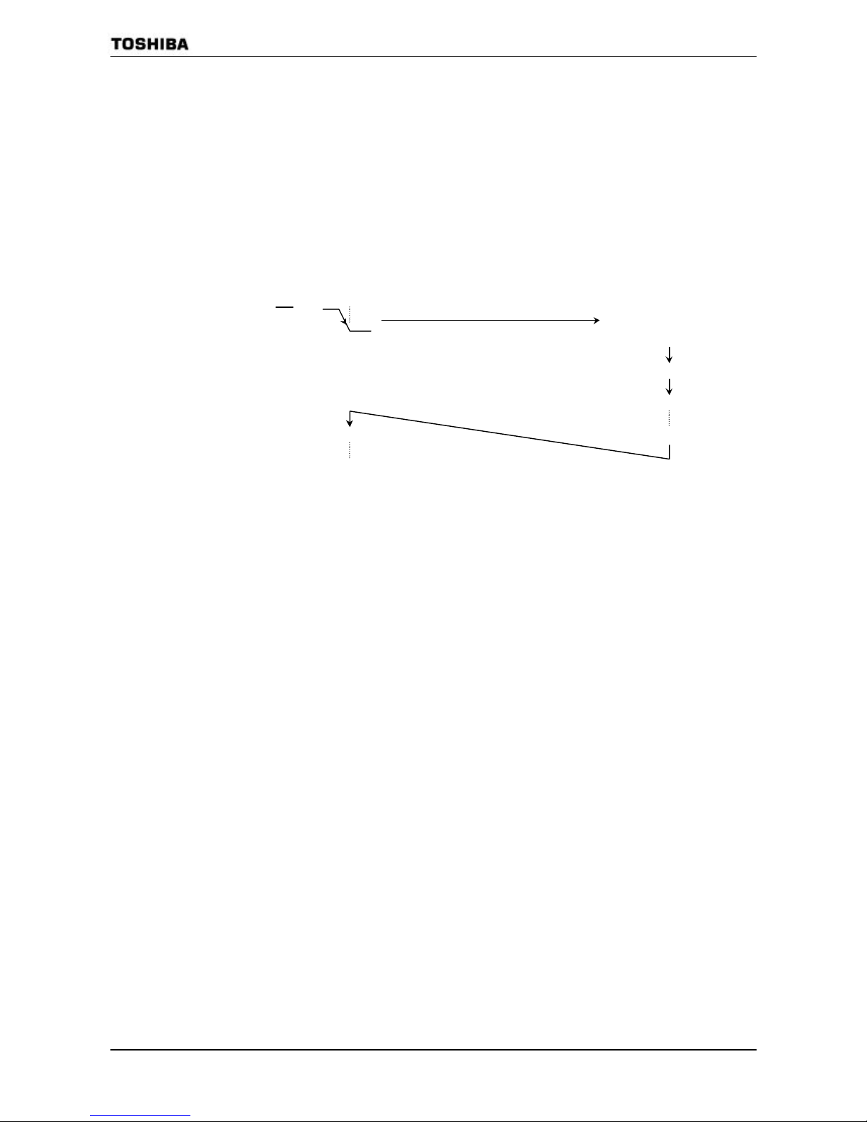
(Setting Example)
The Stop mode is entered when the low frequency operates, and high frequency operates after releasing
due to NMI.
Address
SYSCR0
EQU 00E0H
SYSCR1
EQU 00E1H
SYSCR2
EQU 00E2H
8FFDH LD (SYSCR1), 08H ; f
SYS
= fs/2
9000H LD (SYSCR2), X−1001X1B
; Sets Warming Up Time to 214/f
OSCH
9002H LD
(SYSCR0), 011000
− −
B
; Operates High Frequency after released.
− : no change
9005H
HALT
NMI
9006H LD XX, XX RETI
Clears and starts hit
warm-up timer
(high-frequency)
end
NMI Interrupt Routine
Note: When different modes are used before and after STOP mode as the above mentioned , there is possible
to release the HALT mode without changing the operation mode by acceptance of the halt release
interrupt request during execution of “HALT” instruction (during 8 state).In the system which accepts
the interrupts during execution ”HALT” instruction, set the same operation mode before and after the
STOP mode.
Page 38
TMP91C824
91C824-
35
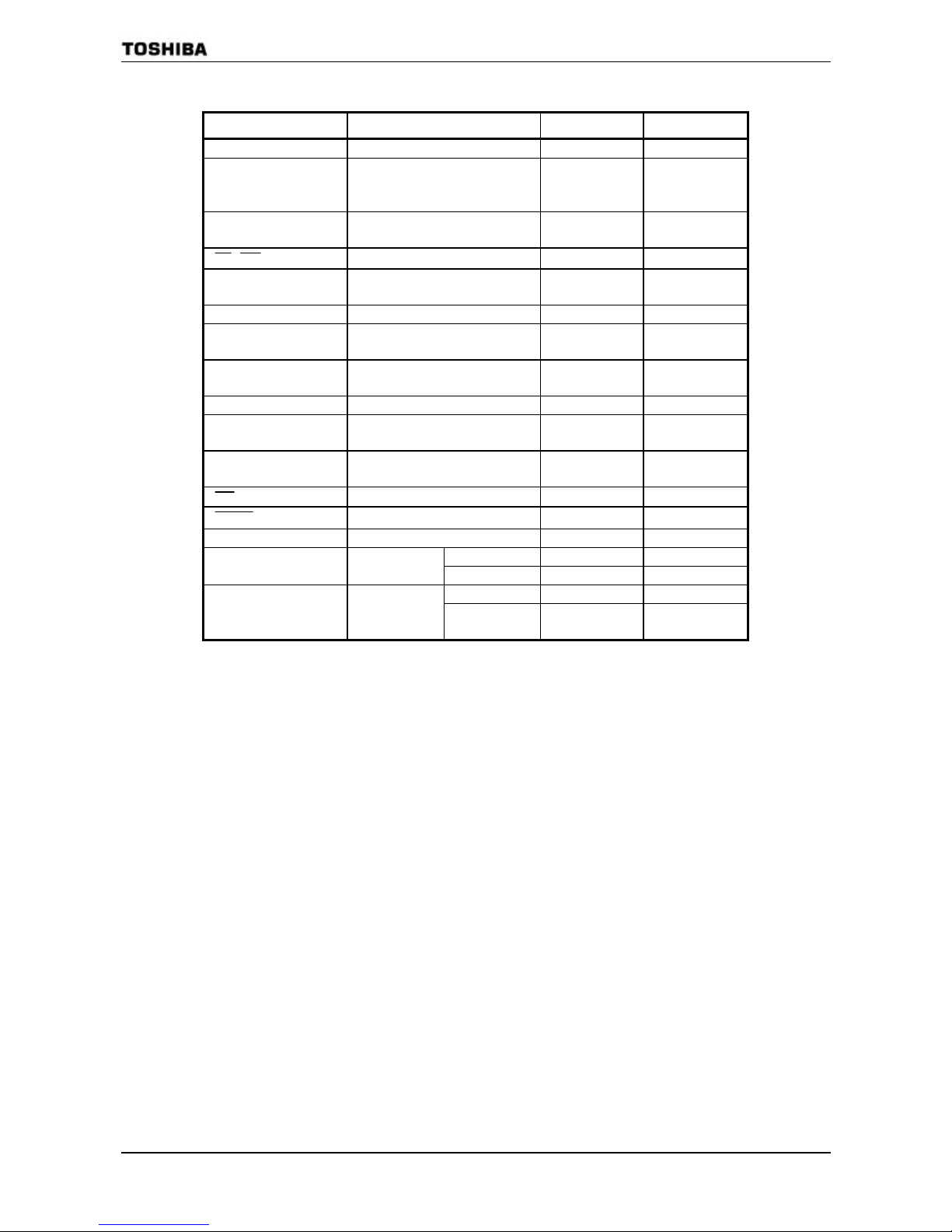
Table 3.3.6 Pin states in IDLE1/Stop Mode
Pin name Input/Output <DRVE> = 0 <DRVE> = 1
D0∼7 I/O
− −
P10∼17(D8∼15? Input mode
Output mode
I/O
−
−
−
−
Output
−
P20∼27(A16∼23),A0∼15,P
D0∼PD7
Output pin
−
Output
RD , WR
Output pin
−
‘1’ output
P52∼56 Input mode
Output mode
−
−
Input
Output
P60∼P64 Output pin
−
Output
P70-71 Input mode
Output mode
−
−
Input
Output
P72 Input mode
Output mode
Input
−
Input
Output
P80∼P87 Input pin
− −
PB0∼PB2,PC0∼PC5 Input mode
Output mode
−
−
Input
Output
PB3∼PB6 Input mode
Output mode
Input
−
Input
Output
NMI
Input pin Input Input
RESET
Input Input Input
AM0, AM1 Input Input Input
IDLE1 Input Input X1,XT1
Input
STOP
− −
IDLE1 Output Output X2,XT2 Output
STOP “H” Level output
XT2 is Hi-Z
“H” Level output
XT2 is Hi-Z
− : Input for input mode/input pin is invalid; output mode/output pin is at high impedance.
Input : Input gate in operation. Fix input vol tage to “L” or “H” so that input pin stays constant.
Output: Output state
Page 39

TMP91C824
91C824-36
3.4 Interrupts
Interrupts are controlled by the CPU Interrupt Mask Register SR<IFF2:0> and by the
built-in interrupt controller.
The TMP91C824 has a total of 37 interrupts divided into the following five types:
• Interrupts generated by CPU: 9 sources
(Software interrupts,Illegal Instruction interrupt)
• Internal interrupts: 23 sources
• Interrupts on external pins (NMI and INT0 to INT3): 5 sources
A (fixed) individual interrupt vector number is assigned to each interrupt.
One of seven (variable) priority level can be assigned to each maskable interrupt.
The priority level of non-maskable interrupts are fixed at 7 as the highest level.
When an interrupt is generated, the interrupt controller sends the piority of that interrupt to the CPU.If
multiple interrupts are generated simultaneo usly, the interrupt controller sends t he interrupt with the highest
priority to the CPU.(The highest priority is level 7 using for non-maskable interrupts.)
The CPU compares the priority level of the interrupt with the value of the CP U interrupt mask register
<IFF[2:0]>. If the priority level of the interrupt is higher than the value of the interrupt mask register, the CPU
accepts the interrupt.
The interrupt mask register <IFF[2:0]> value can be updated using the value of the EI instruction (“EI num”
sets <IFF[2:0]> data to num).
For example, specifying “EI 3” enables the maskable interrupts which priorit y level set in the interrupt
controller is 3 or higher, and also non-maskable interrupts.
Operationally, the DI instruction (<IFF[2:0]> =”7”) is identical to the “EI 7” instructio n. DI instruction is
used to disable maskable interrupts because of the priority level of maskable interrupts is 0 to 6. The EI
instruction is vaild immediately after execution.
In addition to the above general-purpose interrupt processing mode, TLCS-900/L1 has a micro DMA
interrupt processing mode as well. The CPU can transfer the data (1/2/4 bytes) automatically in micro DMA
mode, therefore this mode is used for s peed-up in terru pt proces sing , such as t ransferri ng data t o the in ternal or
external peripheral I/O. Moreov er,TMP91C824 h as s oftw are start fu nction for mi cro DMA processing request
by the software not by the hardware interrupt.
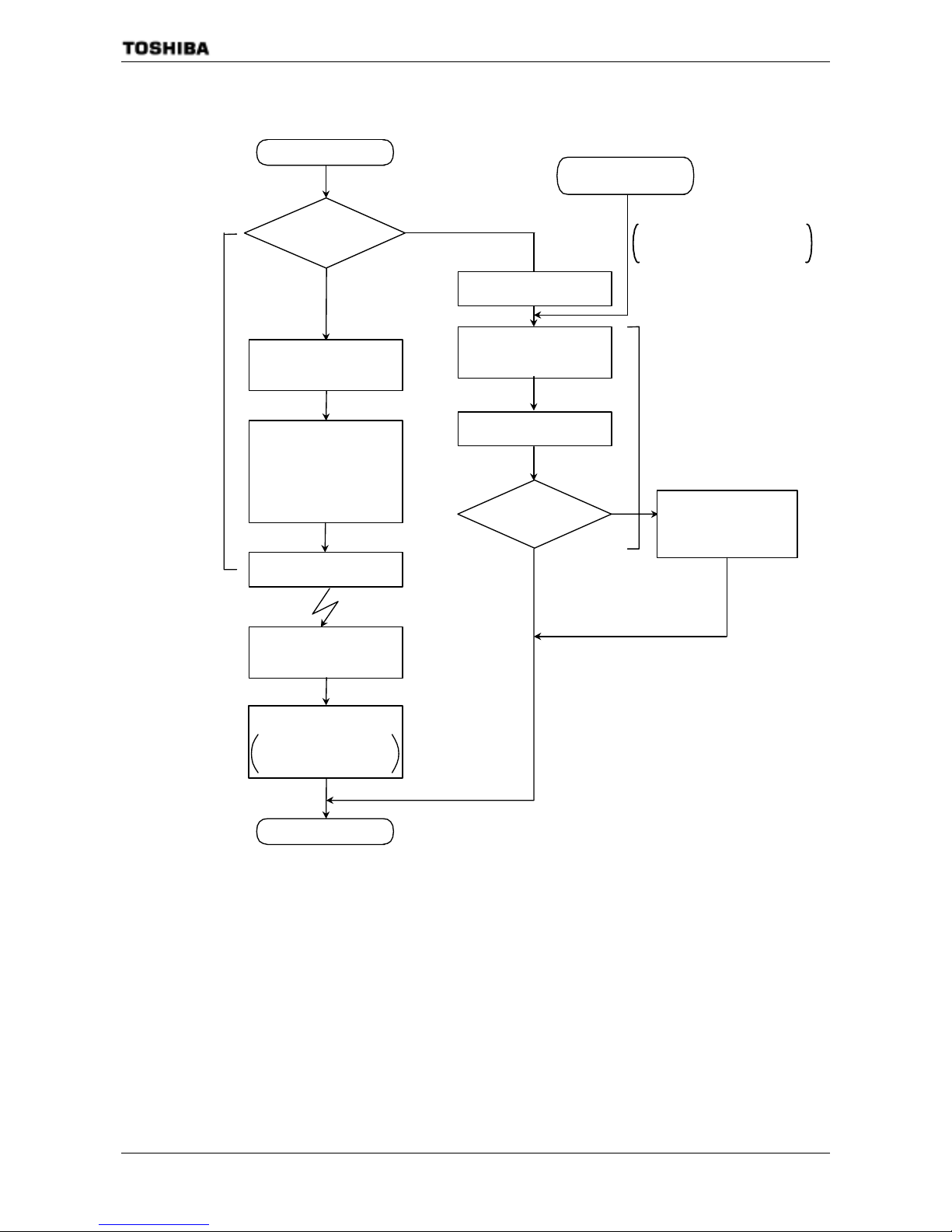
Figure 3.4.1 shows the overall interrupt processing flow.
Page 40
TMP91C824
91C824-37
General-purpose
interrupt
processing
Interrupt specified
by micro DMA
start vector?
Yes
Interru pt pr oc ess i ng
PUSH PC
PUSH SR
SR<IFF2:0> ←Level of
accepted
interrupt + 1
INTNEST ← INTNEST + 1
End
PC ← (FFFF00H + V)
Interru pt pr oc ess i ng
program
Count ← Count−1
Count = 0
No
Yes
Data transfer by micro
DMA
No
Micro DMA processing
RETI instruction
POP SR
POP PC
INTNEST
←
INTNEST − 1
Clear vector regist er
generating micro DMA
trasfer and interru pt
(INTTC0 – 3)
Clear interrupt requenst flag
Interrupt vector value “V”
read
Interrupt request F/F clear
Micro DMA soft start
request
Pr esu p poses that o ne of four
channels of micro DMA start
vector register is set to FCH.
Figure 3.4.1 Overall interrupt processing flow
Page 41

TMP91C824
91C824-38
3.4.1 General-purpose interrupt processing
When the CPU accepts an interrupt, it usually performs the following sequence of operations. That is
also the same as TLCS-900/L and TLCS-900/H.
(1) The CPU reads the interrupt vector from the interrupt controller.
If the same level interrupts occur simultaneously, the interrupt controller generates an interrupt
vector in accordance with the default priority and clears the interrupt request.
(The default priority is already fixed for each interrupt: the smaller vector value has the higher
priority level.)
(2) The CPU pushes the value of Program Counter(PC) and Status Register(SR) onto the stack area
(indicated by XSP).
(3) The CPU sets the value which is the priority level of the accepted interrupt plus 1(+1) to the
Interrupt Mask Register <IFF[2:0]>. However, if the priority level of the accepted interrupt is 7, the
register’s value is set to 7.
(4) The CPU increases the interrupt nesting counter INTNEST by 1(+1).
(5) The CPU jumps to the address indicated by the data at address “FFFF00H + interrupt vector” and
starts the interrupt processing routine.
The above processing time is 18-states(2.25usec. at 16MHz) as the best case(16bits data-b us width
and 0-wait).
When the CPU compled the interrupt processing, use t he RETI instruction to return to the main
routine. RETI restores the contents of Program Counter(PC) and Status Register(SR) from the stack
and decreases the Interrupt Nesting counter INTNEST by 1(-1).
Non-maskable interrupts cannot be disabled by a user program. Maskable interrupts, however, can
be enabled or disabled by a user program. A program can set the priority level for each interrupt
source. (A priority level setting of 0 or 7 will disable an interrupt request.)
If an interrupt request which has a priority level equal to or greater than the value of the CPU
Interrupt Mask Register <IFF[2:0]> comes out, the CPU accepts its interrupt. Then, the CPU
Interrupt Mask Register <IFF[2:0]> is set to the value of the priority level for the accepted interru pt
plus 1(+1).
Therefore, if an interrupt is generated with a higher level than the current interrupt during its
processing, the CPU accepts the later interrupt an d goes to the n esting st atus of interru pt processi ng.
Moreover, if the CPU receives another interrupt request while performing the said (1) to (5)
processing steps of the current interrupt, the latest interrupt request is sampled immediat ely after
execution of the first instruction of the current interrupt processing routine. Specifying DI as the
start instruction disables maskable interrupt ne sting.
A Reset initializes the Interrupt Mask Register <IFF[2:0]> to “111”, disabling all maskable
interrupts.
Table 3.4.1 shows the TMP91C824 interrupt vectors and micro DMA start vectors. The address
FFFF00H to FFFFFFH (256 bytes) is assigned for the interrupt vector area.
Page 42
TMP91C824
91C824-39
Table 3.4.1 TMP91C824 interrupt vectors table
Default
Priority
Type Interrupt source and source of micro DMA request
Vector
value(V)
Vector
reference
Address
Micro
DMA
start vector
1
"Reset" or 「SWI 0」instruction
0000H FFFF00H
−
2
「SWI 1」instruction
0004H FFFF04H
−
3
INTUNDEF: illegal instruction or 「SWI 2」instruction
0008H FFFF08H
−
4
「SWI 3」instruction
000CH FFFF0CH
−
5
「SWI 4」instruction
0010H FFFF10H
−
6
「SWI 5」instruction
0014H FFFF14H
−
7
「SWI 6」instruction
0018H FFFF18H
−
8
「SWI 7」instruction
001CH FFFF1CH
−
9
NMI
pin
0020H FFFF20H
−
10
Non-
Maskable
INTWD: Watchdog timer 0024H FFFF24H
−
– Micro DMA (MDMA)
− − −
11 INT0 pin 0028H FFFF28H 0AH
12 INT1 pin 002CH FFFF2CH 0BH
13 INT2 pin 0030H FFFF30H 0CH
14 INT3 pin 0034H FFFF34H 0DH
15 INTALM0: ALM0(8KHz) 0038H FFFF38H 0EH
16 INTALM1: ALM1(512Hz) 003CH FFFF3CH 0FH
17 INTALM2: ALM2(64Hz) 0040H FFFF40H 10H
18 INTALM3: ALM3(2Hz) 0044H FFFF44H 11H
19 INTALM4: ALM4(1Hz) 0048H FFFF48H 12H
20 INTTA0 : 8 bit timer0 004CH FFFF4CH 13H
21 INTTA1 : 8 bit timer1 0050H FFFF50H 14H
22 INTTA2 : 8 bit rimer2 0054H FFFF54H 15H
23 INTTA3 : 8 bit timer3 0058H FFFF58H 16H
24 INTRX0 : serial reception (channel. 0) 005CH FFFF5CH 17H
25 INTTX0 : serial transmission (channel. 0) 0060H FFFF60H 18H
26 INTRX1 : serial reception (channel. 1) 0064H FFFF64H 19H
27 INTTX1 : serial transmission (channel. 1) 0068H FFFF68H 1AH
28 INTAD : A/D conversion end 006CH FFFF6CH 1B H
29 INTRTC : RTC (alarm interrupt) 0074H FFFF74H 1 DH
30 INTSBI : SBI interrupt 0078H FFFF78H 1EH
31 INTP0 : Protect0 (WR to special SFR) 0080H FFFF80 H 2 0H
32 INTP1 : Protect1 (WR to ROM) 0084H FFFF84H 21H
33 INTTC0 : Micro DMA end (channel. 0) 0088H FFFF88H -34 INTTC1 : Micro DMA end (channel. 1) 008CH FFFF8CH -35 INTTC2 : Micro DMA end (channel. 2) 0090H FFFF90H -36 INTTC3 : Micro DMA end (channel. 3) 0094H FFFF94H --
Maskable
(Reserved)
:
(Reserved)
0098H
:
00FCH
FFFF98H
:
FFFFFCH
−
:
−
Page 43

TMP91C824
91C824-40
3.4.2 Micro DMA processing
In addition to general-purpose interrupt process ing, the TMP91C824 su pprots a m icro DMA function.
Interrupt requests set by micro DMA perform micro DMA processing at the highest priority level (level
6) among maskable interrupts, regardless of the priority level of the particular interrupt source. Micro.
The micro DMA has 4 channels and is possible continuous transmission by specifing the say later burst
mode.
Because the micro DMA function has been implemented wi th the cooperative operation of C PU, when
CPU goes to a stand-by mode b y HALT instruction, the requirement of micro DM A will be ignored
(pending).
(1) Micro DMA operation
When an interrupt request specified by the micro DMA start vector register is generated, the
micro DMA triggers a micro DMA request to the CPU at interrupt priority level 6 and starts
processing the request in spite of any interrupt source’s level. The micro DMA is ignored on
<IFF[2:0]>=”7”.
The 4 micro DMA channels allow micro DMA proces sing t o be set for up t o 4 ty pes of interru pts at
any one time. When micro DMA is accepted, the interrupt request flip-flop assigned to th at channel
is cleared.
The data are automatically transferred once(1/2/4 bytes) from the transfer source address to the
transfer destination address set in the control reg ister, an d the trans fer coun ter is decreas ed by 1(-1).
If the decreased result is “0”, the micro DMA transfer end interrupt (INTTC0 to INTTC3) passes
from the CPU to the interrupt controller. In addition, the micro DMA start vector register DMAnV
is cleared to 0, the next micro DMA is disabled and micro DMA processing completes. If the
decreased result is other than “0”, the micro DMA processing completes if it isn’t specified the say
later burst mode. In this case, the micro DM A transfer end interrupt (INTT C0 to INTTC3) aren’t
generated.
If an interrupt request is triggered for the interrupt source in use during the interval between the
clearing of the micro DMA start vector and the next setting, general-purpose interrupt processing
executes at the interrupt level set. Therefore, if only using the interrupt for starting the micro DMA
(not using the interrupts as a general-purpose interrupt: level 1 to 6), first set the interrupts level to 0
(interrupt requests disabled).
If using micro DMA and general-purpose interrupts together, first set the level of the interrupt used
to start micro DMA processing lower than all the other interrupt levels. In this case, the cause of
general interrupt is limited to the edge interrupt.
The priority of the micro DMA transfer end interrupt (INTTC0 to INTTC3) is defined by the
interrupt level and the default priority as the same as the other maskable interrupt.
If a micro DMA request is set for more than one channel at the same time, the priority is not based
on the interrupt priority level but on the channel number. The smaller channel number has the higher
priority (Channel 0 (high) > channel 3 (low)).
While the register for setting the transfer source/transfer d estination addresses is a 32-bit control
register, this register can only effectively output 24-bit addresses. Accordingly, micro DMA can
access 16M bytes (the upper eight bits of the 32 bits are not valid).
Page 44
TMP91C824
91C824-41
Three micro DMA transfer modes are supported: 1- byt e transf er, 2-by te (one-w ord) transf er, and
4-byte transfer. After a transfer in any mode, the transfer source / destination addresses are
increased, decreased, or remain unchanged.
This simplifies the transfer of data from I/O to memory, from memory to I/O , and from I/O to I/O.
For details of the transfer modes, see 3.4.2 (4) “Transfer Mode Reg ister”. A s the transf er count er is
a 16-bit counter, micro DMA processing can be set for up to 65536 times per interrupt source.(The
micro DMA processing count is maximized when the transfer counter initial value is set to 0000H.)
Micro DMA processing can be started by th e 24 interrupts shown in th e micro DMA s tart vectors
of Table 3.4.1 and by the micro DMA soft start, making a total of 25 interrupts.
Figure 3.4.2 shows the word transfer micro DMA c ycle in transfer destination address INC mode
(except for Counter mode, the same as for other modes).
(The conditions for this cycle are based on an external 16-bit bus, 0 waits, trandfer
source/transfer destination addresses both even-numberd values).
OutputInput
Trasger destination
address
Nex t + 2Next
1 state
D0 to 15
X1
A0 to 23
DM1 DM2 DM3 DM4 DM5 DM6 DM7 DM8
(note1) (note2)
RD
WR/HWR
Trasfer source address
Figure 3.4.2 Timing for micro DMA cycle
States 1~3: Instruction fetch cycle (gets next address code).
If 3 bytes and more instruction codes are inserted in the instruction queue
buffer, this cycle becomes a dummy cycle.
States 4~5: Micro DMA read cycle
State 6: Dummy cycle (the address bus remains unchanged from state 5)
States 7~8: Micro DMA write cycle
(note1): If the source address area is an 8-bit bus, it is increased by two states.
If the source address area is a 16-bit bus and th e address st arts from an odd number, i t is increas ed by
two states.
(note2): If the destination address area is an 8-bit bus, it is increased by two states.
If the destination address area is a 16-bit bus and the address starts from an odd number, it is
increased by two states.
Page 45
TMP91C824
91C824-42
(2) Soft start function
In addition to starting the micro DMA function b y i nterrupts, TMP91C824 includes a micro
DMA software start function that starts micro DM A on the generation of the write cycle to the
DMAR register.
Writing “1” to each bit of DMAR register causes micro DMA once. At the end of transfer, the
corresponding bit of the DMAR register is automatically cleared to “0”.
Only one-channel can be set once for micro DMA. (Do not write “1” to plural bits.)
When writing again “1” to the DMAR register, check whether the bit is “0” before writing “1”.
When a burst is specified by DMAB register, data is continuously transferred until the value in the
micro DMA transfer counter is “0” after start up of the micro DMA.
Symbol NAME Address 7 6 5 4 3 2 1 0
DMA Request
DMAR3 DMAR2 DMAR1 DMAR0
R/W
DMAR
DMA
Request
Register
89h
(no RMW)
0 0 0 0
(3) Transfer control registers
The transfer source address and the transfer destination address are set in the following registers
in CPU. Data setting for these registers is done by an “LDC cr,r” instruction.
Channel 0
DMAS0 DMA Sourc e address reg is t er 0 : onl y us e LSB 24 bits
DMAD0 DMA Destination addr ess reg is ter 0 : only use LSB 24bi ts
DMAC0 DMA Counter register 0 : 1 to 65536
DMAM0 DMA Mode regis t er 0
Channel 3
DMAS3 DMA Sourc e address reg is t er 3
DMAD3 DMA Destination address register 3
DMAC3 DMA Counter register 3
DMAM3 DMA Mode regis t er 3
8 bits
16 bits
32 bits
Page 46
TMP91C824
91C824-43
(4) Detailed descrip tion of the Transfer Mode Register
8 bits
0 0 0 Mode
Number of
Transfer Bytes
Mode Descripti on
Number of
Execution States
Minimum
Execution Time
@ fc = 16 MHz
000
(fixed)
000
00 Byte transfer
8 states
1000 ns
01 Word transfer
12 sates 1500 ns
10 4-byte transfer
Transfer Destination Address INC Mode
・・・・・・・・・・・・・・・・・・・・・・・・・・・
I/O to memory
(DMADn+) ← (DMASn)
DMACn ← DMACn − 1
If DMACn = 0, then INTTCn is generated.
001
00 Byte transfer
8 states
1000 ns
01 Word transfer
12 sates 1500 ns
10 4-byte transfer
Transfer Destination Address DEC Mode
・・・・・・・・・・・・・・・・・・・・・・・・・・・
I/O to memory
(DMADn−) ← (DMASn)
DMACn ← DMACn − 1
If DMACn = 0, then INTTCn is generated.
010
00 Byte transfer
8 states
1000 ns
01 Word transfer
12 sates 1500 ns
10 4-byte transfer
Transfer Source Address INC Mode
・・・・・・・・・・・・・・・・・・・・・・・・・・・
Memory to I/O
(DMADn) ← (DMASn+)
DMACn ← DMACn − 1
If DMACn = 0, then INTTCn is generated.
011
00 Byte transfer
8 states
1000 ns
01 Word transfer
12 sates 1500 ns
10 4-byte transfer
Transfer Source Address DEC Mode
・・・・・・・・・・・・・・・・・・・・・・・・・・・
Memory to I/O
(DMADn) ← (DMASn−)
DMACn ← DMACn − 1
If DMACn = 0, then INTTCn is generated.
100
00 Byte transfer
8 states
1000 ns
01 Word transfer
12 sates 1500 ns
10 4-byte transfer
Fixed Address Mode
・・・・・・・・・・・・・・・・・・・・・・・・・・・・・・・
I/O to I/O
(DMADn) ← (DMASn−)
DMACn ← DMACn − 1
If DMACn = 0, then INTTCn is generated.
101 00 C ounter Mod e
・・・・・・・・・・・
For counting number of t imes interrupt is generated
DMASn ← DMASn + 1
DMACn ← DMACn − 1
If DMACn = 0, then INTTCn is generated.
5 sates 625 ns
(note): When setting a value in this register, write 0 to the upper 3
bits.
DMAM0 to
DMAM3
(note1): “n” is the corresponding micro DMA channels 0 to 3
DMADn +/DMASn+ : Post-increment (increment register value after transfer)
DMADn −/DMASn− : Post-decrement (decrement register value after transfer)
The I/Os in the table mean fixed address and the memory means increment(INC) or
decrement(DEC) addresses.
(note2): Execution time is under the condition of:
16bit bus width(both translation and destination address area) / 0 wait /
fc = 16MHz / selected high frequency mode (fc x 1)
(note3): Do not use an un defined code for th e tran sfer m ode regis ter except f or the def ined codes lis ted in the
above table.
Page 47

TMP91C824
91C824-44
3.4.3 Interrupt controller operation
The block diagram in F igure 3.4.3 sh ows th e interru pt circuits. The left-h and side of the diagram shows
the interrupt controller circuit. The right-hand side shows the CPU interrupt request signal circuit and the
halt release circuit.
For each of the 36 interrupt channels there is an interrupt request flag (consisting of a flip-flop), an
interrupt priority setting register and a micro DMA start vector register. The interrupt request flag latches
interrupt requests from the peripherals. The flag is cleared to zero in the following cases:
! when reset occurs
! when the CPU reads the channel vector after accepted its interrupt
! when executing an instruction that clears the interrupt (write DMA start vector to INTCLR
register)
! when the CPU receives a micro DMA request (when micro DMA is set)
! when the micro DMA burst transfer is terminated
An interrupt priority can be set independently for each interrupt source by writing the priority to the
interrupt priority setting register (e.g. INTE 0AD or INTE12). 6 interrupt priorities levels (1 to 6) are
provided. Setting an interrupt source’s priority level to 0 (or 7) disables interrupt requests from that source.
The priority of non-maskable interrupts (NMI pin interrupts and Watch dog Timer interrupts) is fixed at 7.
If interrupt request with the same level are generated at the s ame time, the default pr iority (the interrupt
with the lowest priority or, in other words, the interrupt with the lowest vector value) is used to determine
which interrupt request is accepted first.
The 3rd and 7th bits of the interrupt priority setting register indicate the state of the interrupt request flag
and thus whe ther an interrupt request for a given channel has occurred.
The interrupt controller sends the interrupt request with the highest priority among the simulateous
interrupts and its vector address to the CPU. The CPU compares the prio rity value <IFF[2:0]> in the
Status Register by the interrupt request signal with the priority value set;if the latter is higher, the interrupt
is accepted. Then the CPU sets a value higher th an the priority value by 1(+1) in the C PU SR <IFF[2:0]>.
Interrupt request where the priority value equals or is higher than the set value are accepted
simultaneously during the previous interrupt routine.
When interrupt processing is completed (after execution of the RETI instruction), the CPU restores the
priority value saved in the stack before the interrupt was gene r a ted to the CPU SR<IFF[2:0]>.
The interrupt controller also has registers(4 channels) used to store the micro DMA start vector.
Writing the start vector of the interrupt source for the micro DMA processing (see Table 3.4.1), enables
the corresponding interrupt to be processed by micro DMA processing. T he values must be set in the
micro DMA parameter register (e.g. DMAS and DMAD) prior to the micro DMA processing.
Page 48
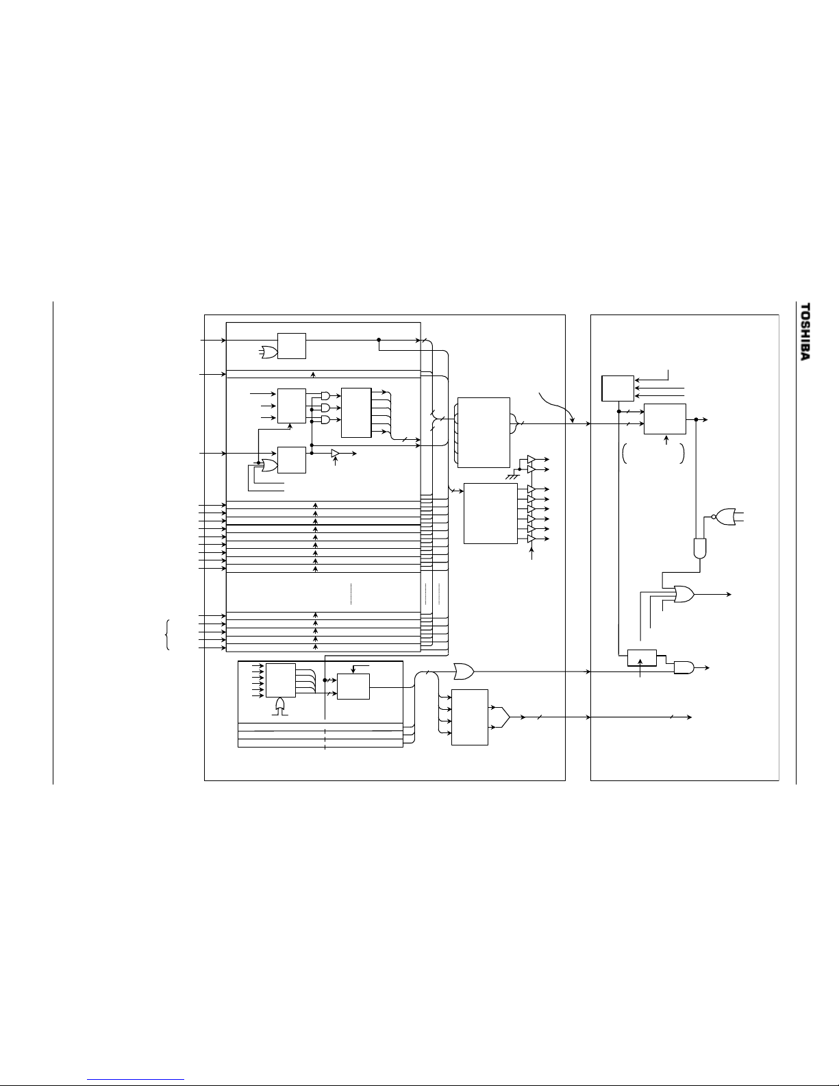
TMP91C824
91C824-45
Interrupt request
si
g
nal to CPU
if IFF = 7 then 0
Micro DMA start vector setting register
INTP1
INTTC0
INTTC1
INTTC2
INTTC3
V = 78H
V = 7CH
V = 80H
V = 84H
V = 88H
Soft start
Micro DMA
Counter
Zero
Interrupt
6
INTTC0
During
IDLE1
32
3
3
3
1
6
1
7
2
2
4
6
34
4 input OR
INT0,1,2,3,RTC,ALM
Micro DMA channel
priority enc oder
Priority encoder
DMA0V
DMA1V
DMA2V
DMA3V
RESET
Interrupt request F/F
RESET
Decoder
Reset
Priority setting regist er
V = 20H
V = 24H
Interrupt controller
CPU
S Q
R
V = 28H
V = 2CH
V = 30H
V = 34H
V = 38H
V = 3CH
V = 40H
V = 44H
V = 48H
V = 4CH
D Q
CLR
Y1
Y2
Y3
Y4
Y5
Y6
A
B
C
Dn
Dn + 1
Dn + 2
Interrupt
request F/F
Interrupt vector read
Micro DMA acknowledge
Interrupt request F/F
Dn + 3
A
B
C
i
nterrupt
vector read
D2
D3
D4
D5
D6
D7
Selector
S Q
R
0
1
2
3
A
B
D0
D1
Interrupt vector
read
Interrupt
mask F/F
Micro DMA request
HALT release
NMI
if INTRQ2∼0 ≥ IFF
2∼0 then 1.
INTRQ2 ∼ 0
IFF2:0
Interrupt
level detect
RESET
EI 1∼7
DI
Interrupt request
signal
During
STOP
Micro DMA channel
specification
RESET
NMI
INTWD
INT0
INT1
INT2
INT3
INTALM0
INTALM1
INTALM2
INTALM3
INTALM4
INTTA0
S
Interrupt vector
generator
Highest
Priority
interrupt
level select
1
2
3
4
5
6
D5
D4
D3
D2
D1
D0
D Q
CLR
Figure 3.4.3 Block Diagram of Interrupt Controller
Page 49
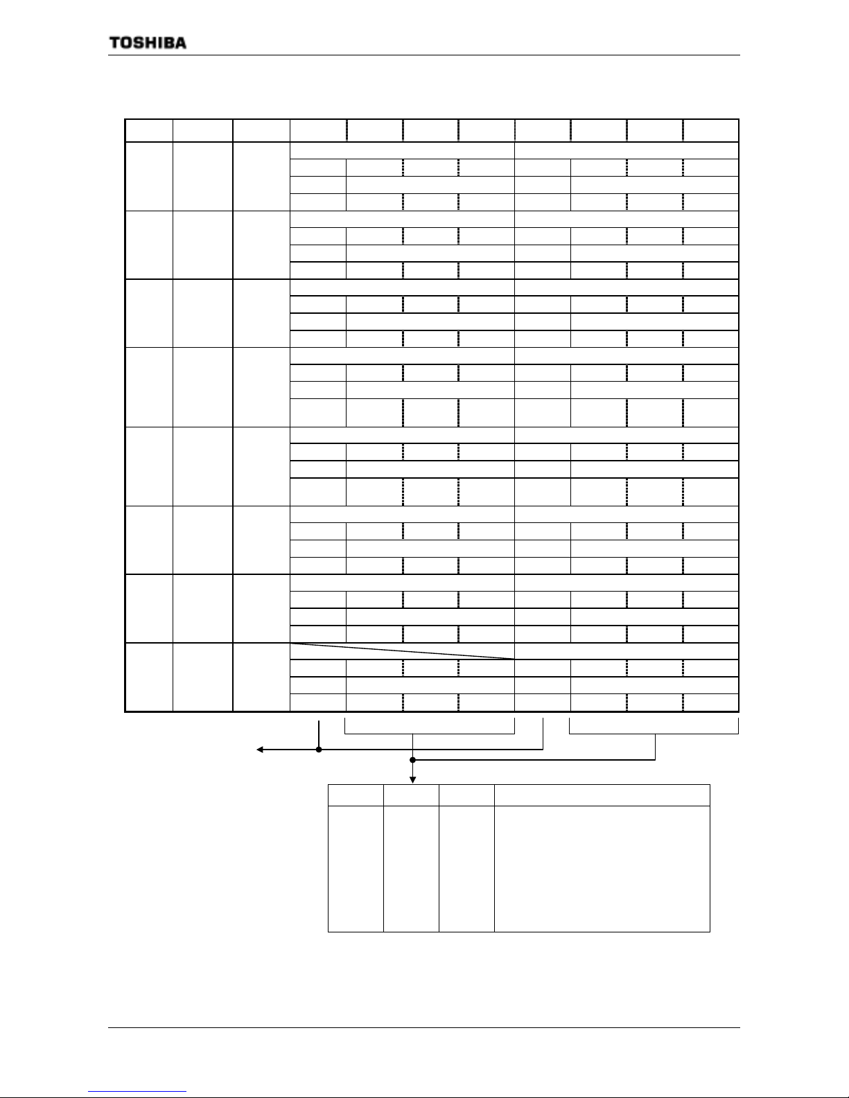
TMP91C824
91C824-46
(1) Interrupt level setting registers
Symbol NAME Address 7 6 5 4 3 2 1 0
INTAD INT0
IADC IADM2 IADM1 IADM0 I0C I0M2 I0M1 I0M0
R R/W R R/W
INTE0AD
INT0 &
INTAD
Enable
90h
0 0 0 0 0 0 0 0
INT2 INT1
I2C I2M2 I2M1 I2M0 I1C I1M2 I1M1 I1M0
R R/W R R/W
INTE12
INT1 &
INT2
Enable
91h
0 0 0 0 0 0 0 0
INTALM4 INT3
IA4C IA4M2 IA4M1 IA4M0 I3C I3M2 I3M1 I3M0
R R/W R R/W
INTE3
ALM4
INT3&
INTALM
4Enable
92h
0 0 0 0 0 0 0 0
INTALM1 INTALM0
IA1C IA1M2 IA1M1 IA1M0 IA0C IA0M2 IA0M1 IA0M0
R R/W R R/W
INTEALM
01
INTALM
0 &
INTALM
1
Enable
93h
0 0 0 0 0 0 0 0
INTALM3 INTALM2
IA3C IA3M2 IA3M1 IA3M0 IA2C IA2M2 IA2M1 IA2M0
R R/W R R/W
INTEALM
23
INTALM
2 &
INTALM
3
Enable
94h
0 0 0 0 0 0 0 0
INTTA1(TMRA1) INTTA0(TMRA0)
ITA1C ITA1M2 ITA1M1 ITA1M0 ITA0C ITA0M2 ITA0M1 ITA0M0
R R/W R R/W
INTETA01
INTTA0
&
INTTA1
Enable
95h
0 0 0 0 0 0 0 0
INTTA3(TMRA3) INTTA2(TMRA2)
ITA3C ITA3M2 ITA3M1 ITA3M0 ITA2C ITA2M2 ITA2M1 ITA2M0
R R/W R R/W
INTETA23
INTTA2
&
INTTA3
Enable
96h
0 0 0 0 0 0 0 0
INTRTC
IRC IRM2 IRM1 IRM0
R R/W
INTERTC
INTRTC
enable
97h
0 0 0 0
Interrupt request flag
lxxM2 lxxM1 lxxM0 Function (Write)
0 0 0 Disables interrupt requests
0 0 1 Sets interrupt priority level to 1
0 1 0 Sets interrupt priority level to 2
0 1 1 Sets interrupt priority level to 3
1 0 0 Sets interrupt priority level to 4
1 0 1 Sets interrupt priority level to 5
1 1 0 Sets interrupt priority level to 6
1 1 1 Disables interrupt requests
Page 50
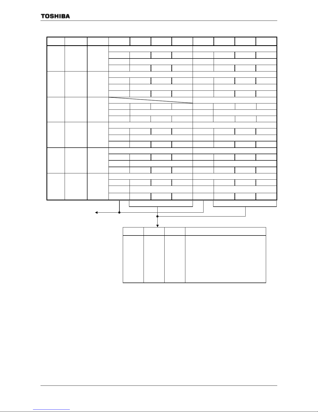
TMP91C824
91C824-47
Symbol NAME Address 7 6 5 4 3 2 1 0
INTTX0 INTRX0
ITX0C ITX0M2 ITX0M1 ITX0M0 IRX0C IRX0M2 IRX0M1 IRX0M0
R R/W R R/W
INTES0
Interrupt
Enable
Serial 0
98H
0 0 0 0 0 0 0 0
INTTX1 INTRX1
ITXT1C ITX1M2 ITX1M1 ITX1M0 IRX1C IRX1M2 IRX1M1 IRX1M0
R R/W R R/W
INTES1
INTRX1 &
INTTX1
Enable
99H
0 0 0 0 0 0 0 0
INTS2
IS2C IS2M2 IS2M1 IS2M0
R R/W
INTES2
INTES2
Enable
9AH
0 0 0 0
INTTC1 INTTC0
ITC1C ITC1M2 ITC1M1 ITC1M0 ITC0C ITC0M2 ITC0M1 ITC0M0
R R/W R R/W
INTET
C01
INTTC0 &
INTTC1
Enable
9BH
0 0 0 0 0 0 0 0
INTTC3 INTTC2
ITC3C ITC3M2 ITC3M1 ITC3M0 ITC2C ITC2M2 ITC2M1 ITC2M0
R R/W R R/W
INTET
C23
INTTC2 &
INTTC3
Enable
9CH
0 0 0 0 0 0 0 0
INTP1 INTP0
IP1C IP1M2 IP1M1 IP1M0 IP0C IP0M2 IP0M1 IP0M0
R R/W R R/W
INTE
P01
INTP0 &
INTP1
Enable
9DH
0 0 0 0 0 0 0 0
In terrupt request flag
lxxM2 lxxM1 lxxM0 Function (Write)
0 0 0 Disables interrupt requests
0 0 1 Sets interrupt priority level to 1
0 1 0 Sets interrupt priority level to 2
0 1 1 Sets interrupt priority level to 3
1 0 0 Sets interrupt priority level to 4
1 0 1 Sets interrupt priority level to 5
1 1 0 Sets interrupt priority level to 6
1 1 1 Disables interrupt requests
Page 51
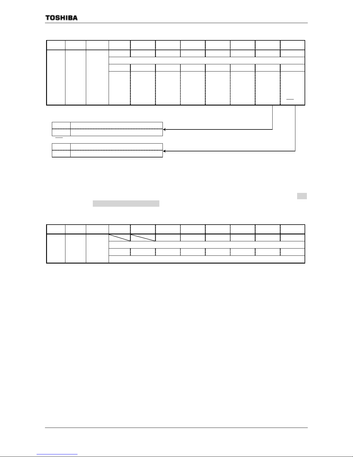
TMP91C824
91C824-48
(2) External interrupt control
Symbol NAME Address 7 6 5 4 3 2 1 0
- I3EDGE I2EDGE I1EDGE I0EDGE I0LE NMIREE
W
0 0 0 0 0 0 0 0
IIMC
Interrupt
Input
Mode
control
8CH
(no RMW)
Always
write”0”
Always
write”0”
INT3EDGE
0: Rising
1: Falling
INT2EDGE
0: Rising
1: Falling
INT1EDGE
0: Rising
1: Falling
INT0EDGE
0: Rising
1: Falling
INT0 mode
0: Edge
1: Level
1: Operates
even on
rising /
falling edge
of
NMI
INT0 level Enable
0 Rising edge detect INT
1 “H” level INT
NMI
rising edge Enable
0 INT request generation at falling edge
1 INT request generation at rising/falling edge
(3) Interrupt request flag clear register
The interrupt request flag is cleared by writing the appropriate micro DMA start vector, as given
in Table 3.4 1, to the register INTCLR.
For example, to clear the interrupt flag INT0, perform the following register operation after
execution of the DI instruction.
INTCLR ← 0AH : Clears interrupt request flag INT0.
Symbol NAME Address 7 6 5 4 3 2 1 0
CLRV5 CLRV4 CLRV3 CLRV2 CLRV1 CLRV0
W
0 0 0 0 0 0
INTCLR
Interrupt
Clear
Control
88H
(no RMW)
Interrupt Vector
(4) Micro DMA start vector registers
This register assigns micro DMA processing to which interrupt source. The interrupt source with
a micro DMA start vector that matches the vector set in this register is assigned as the micro DMA
start source.
When the micro DMA transfer counter value reaches zero, the micro DMA transfer end in terrupt
corresponding to the channel is sent to the interrupt controller, the micro DMA start vector register
is cleared, and the micro DMA start source for the channel is cleared. Therefore, to continue micro
DMA processing, set the micro DMA start vector register again during the processing of the micro
DMA transfer end interrupt.
If the same vector is set in the micro DMA start vector registers of more than one
channel, the
channel with the lowest number has a higher priority.
Accordingly, if the same vector is set in the micro DMA start vector registers of two channels, the
interrupt generated in the channel with the lower number is executed until micro DMA transfer is
complete. If the micro DMA start vector for this channel is not set again, the next micro DMA is
started for the channel with the higher number. (Micro DMA chaining)
Page 52
TMP91C824
91C824-49
Symbol NAME Address 7 6 5 4 3 2 1 0
DMA0 Start Vector
DMA0V5 DMA0V4 DMA0V3 DMA0V2 DMA0V1 DMA0V0
R/W
DMA0V
DMA0
Start
Vector
80H
0 0 0 0 0 0
DMA1 Start Vector
DMA1V5 DMA1V4 DMA1V3 DMA0V2 DMA1V1 DMA1V0
R/W
DMA1V
DMA1
Start
Vector
81H
0 0 0 0 0 0
DMA2 Start Vector
DMA2V5 DMA2V4 DMA2V3 DMA2V2 DMA2V1 DMA2V0
R/W
DMA2V
DMA2
Start
Vector
82H
0 0 0 0 0 0
DMA3 Start Vector
DMA3V5 DMA3V4 DMA3V3 DMA3V2 DMA3V1 DMA3V0
R/W
DMA3V
DMA3
Start
Vector
83H
0 0 0 0 0 0
(5) Micro DMA burst specification
Specifying the micro DMA burst conti nues the micro DMA transfer until the transfer c ounter
register reaches zero after micro DMA start. Setting a bit which corresponds to the micro DMA
channel of the DMAB registers mentioned belo w to “1” specifies a burst.
Symbol NAME Address 7 6 5 4 3 2 1 0
DMAR3 DMAR2 DMAR1 DMAR0
R/W R/W R/W R/W
0 0 0 0
DMAR
DMA
Software
Request
Register
89H
1: DMA Software request
DMAB3 DMAB2 DMAB1 DMAB0
R/W
DMAB
DMA
Burst
Register
8AH
0 0 0 0
Page 53
TMP91C824
91C824-50
(6) Attention point
The instruction execution unit and the bus interface unit of this CPU operate independently.
Therefore, immediately before an interrupt is generated, if the CPU fetches an instruction that clears
the corresponding interrupt request flag, the CPU may execute the instruction that clears the
interrupt request flag(*1) between accepting and reading the interrupt vector. In this case, the CPU
reads the default vector 0008H and reads the interrupt vector address FFFF08H.
To avoid the avobe plogram, place instructions that clear interrupt request flags after a DI
instruction.
In the case of changing the value of the interrupt mask register <IFF2:0> by execution of POP SR
instruction, disable an interrupt by DI instruction before execution of POP SR instruction.
In addition, take care as the following 2 circuits are exceptional and demand special atte nti on.
In Level Mode INT0 is not an edge-triggered interrupt. Hence, in Level
Mode the interrupt request flip-flop for INT0 does not function. The
peripheral interrupt request passes through the S input of t he flip-flop and
becomes the Q output. If the interrupt input mode is changed from Edge
Mode to Level Mode, the interrupt request flag is cleared automatically.
INT0 Lev e l M o d e
If the CPU enter s th e interr up t respons e sequ enc e as a r esult of INT0 goi ng
from 0 to 1, INT0 must then be held at 1 until the interrupt response sequence
has been completed. If INT0 is set to Level Mode so as to release a Halt state,
INT0 must be held at 1 from the time INT0 changes from 0 to 1 until the Halt
state is released. (Hence, it is necessary to ensure that input noise is not
interpreted as a 0, causing INT0 to revert to 0 before the Halt state has been
released.)
When the mode cha nges from Level Mod e to Edge M ode, interru pt requ est
flags which were set in Level Mode will not be cleared. Interrupt request
flags must be cleared using the following sequence.
DI
LD (IIMC) , 00H ; Sw itc he s i nter ru pt i nput mo de f ro m L e vel Mode to
Edge Mode.
LD (INTCLR), 0AH; Clears interrupt request flag.
EI
INTRX The interrupt request flip-flop can only be cleared by a Reset or by reading
the Serial Channel Receive Buffer. It cannot be cleared by an instruction.
(note): The following instructions or pin input state changes are equivalent to instructions that clear the
interrupt request flag.
INT0: Instructions which switch to Level Mode after an interr upt r e quest has been
generated in Edge Mode.
The pin input change from High to Low after interrupt request has been generated
in Level Mode. (H → L)
INTRX: Instruction which read the Receive Buffer
Page 54
TMP91C824
91C824-51
3.5 Port Functions
The TMP91C824 features 56 bit settings which relate to the various I/O ports.
As well as general-purpose I/O port functionality, the po rt pins also have I/O functions which relate to the
built-in CPU and internal I/Os. Table 3. 5.1 lists the functions of each port pin. Table 3.5.2 lists I/O registers and
their specifications.
Table 3.5.1 Port functions
(R: PU= with programmable pull-up resistor / U= with pull-up resistor)
Port name Pin name
Number of
pins
Direction R
Direction
Setting unit
Pin name for built-in function
−
Port 2 P20 to P27 8 Output
−
(
Fixed
)
A16 to A23
Port 5 P54 1 I/O PU Bit
______
P55 1 I/O PU Bit
______
BUSAK
P56 1 I/O PU Bit
_____
WAIT
Port 6 P60 1 Output
−
(
Fixed
)
/CS0
P61 1 Output
−
(Fixed) /CS1
P62 1 Output
−
(Fixed) /CS2,/CS2A
P63 1 Output
−
(Fixed) /CS3
P64 1 Output
−
(Fixed) EA24,/CS2B
P65 1 Output
−
(Fixed) EA25,/CS2C
P66 1 Output
−
(Fixed) /CS2D
P67 1 Output
−
(Fixed) /CS2E
Port 7
P70
P71
P72
1
1
1
I/O
I/O
I/O
−
PU
PU
Bit
Bit
Bit
SCK,OPTRX0
SO/SDA,OPTTX0
SI/SCL
Port 8 P80 to P87 8 Input
−
(Fixed)
AN0 to AN7,
ADTRG
(P83)
−
PB1 1 I/O
−
Bit TA1OUT
PB2 1 I/O
−
Bit TA3OUT
PB3 1 I/O
−
Bit INT0
PB4 1 I/O
−
Bit INT1
PB5 1 I/O
−
Bit INT2
PB6 1 I/O
−
Bit INT3
−
PC1 1 I/O
−
Bit RXD0
PC2 1 I/O
−
Bit
SC
LK0/
0CTS
PC3 1 I/O
−
Bit TXD1
PC4 1 I/O
−
Bit RXD1
PC5 1 I/O
−
Bit
SCLK1/
CTS1
−
PD6 1 Output
−
(
Fixed
)
ALARM,/MLDALM
PD7 1 Output
−
(
Fixed
)
MLDALM
Port Z PZ2 1 I/O P
U
Bit
____
PZ3 1 I/O PU Bit
R/
__
W
Page 55
TMP91C824
91C824-52
Table 3.5.2 I/O Registers and Specifications (1/2) X: Don’t care
I/O reg ister
Port Pin name Specification
Pn PnCR PnFC PnFC2
Input port X 0
Output port X 1
Port 1
(note1)
P10 to P17
D8 to D15 bus X X
None
Output port X 0 Port 2 P20 to P27
A16 to A23 output X
None
1
Input port (Without PU) 0 0 0
Input port (with PU) 1 0 0
P54 to P56
Output port X 1 0
______
BUSRQ input (Without PU)
0 0 1
P54
______
BUSRQ input (With PU)
1 0 1
P55
______
BUSAK output
X 1 1
_____
WAIT input (Without PU)
0 0
Port 5
P56
_____
WAIT input (With PU)
1 0
None
None
P60 to P64 Output port X 0 0
P60 /CS0 output X 1
P61 /CS1 output X 1
None
/CS2 output X 1 0 P62
/CS2A output X X 1
P63 /CS3 output X 1
None
EA24 output X 1 0 P64
/CS2B output X X 1
EA25 output X 1 0 P65
/CS2C output X X 1
P66 /CS2D output X 0 1
Port 6
P67 /CS2E output X
None
0 1
Input port (without PU) 0 0 0 0
Input port (With PU) 1 0 0 0
P70 to P72
Output port X 1 0 0
SCK input X 0 0 0
SCK output X 1 1 0
P70
OPTRX0 input (note2) 1 0 X 1
SDA input X 0 0 0
SDA output (note3) X 1 1 0
SO output X 1 1 0
P71
OPTTX0 output (note2) 1 1 X 1
SI input X 0 0 0
SCL input X 0 0 0
Port 7
P72
SCL output (note3) X 1 1 0
Page 56
TMP91C824
91C824-53
Table 3.5.3 I/O Registers and Specifications (2/2) X: Don’t care
I/O reg ister
Port Pin name Specification
Pn PnCR PnFC PnFC2
Input port X P80 to P87
AN0 to 7 input (n ote4) X
Port 8
P83
______
ADTRG input (note5)
X
None
Input port X 0 0 PB0 to PB6
Output port X 1 0
PB0 TA0IN input X 0 None
PB1 TA1OUT output X 1 1
PB2 TA3OUT output X 1 1
PB3 INT0 input X 0 1
PB4 INT1 input X 0 1
PB5 INT2 input X 0 1
Port B
PB6 INT3 input X 0 1
Input port X 0 0 PC0 to PC5
Output port X 1 0
PC0 TXD0 output (Note2) 1 1 1
PC1 RXD0 input (Note2) (Note6 ) 1 0 None
SCLK0 input (Note2) 1 0 0
SCLK0 output (Note2) 1 1 1
PC2
_____
CTS0 input (Note2)
1 0 0
PC3 TXD1 output (Note2) 1 1 1
PC4 RXD1 input (Note2) 1 0 None
SCLK1 input (Note2) 1 0 0
SCLK1 output (Note2) 1 1 1
Port C
PC5
_____
CTS1 input (Note2)
1 0 0
PD5 to PD7 Output port X 0
PD5 SCOUT output X 1
/ALARM output 1 1 PD6
/MLDALM output 0 1
Port D
PD7 MLDALM output X
None
1
Input port (Without PU) 0 0 0
Input port (with PU) 1 0 0
PZ2 to PZ3
Output port X 1 0
PZ2
____
HWR output
X 1 1
Port Z
PZ3
R/
__
W output
X 1 1
None
(note1): PORT1 is only use for PORT or DATA bus(D8 to D15) by setting AM1 and AM0 pins.
(note2): As for input ports of SIO1 and SIO2: (OPTRX0,OPTTX0,TXD0,TRX0,SCCLK0,/CTS0, TXD1,TRX1,SCCLK1,/CTS1),
logical selection for output data or input data is det erm ined by the output latch register Pn of each port.
(note3): In case using P71 and P72 for SDA and SCL as open-drain ports, set to P7ODE<ODE P71:ODEP72>.
(note4): In case using P80 to P87 for analog input ports of A/D converter, set to ADMOD1<ADCH2:ADCH1:ADCH0>.
(note5): In case using P83 for ADTRG input port, set to ADMOD1<ADTRGE>.
(note6): In case using PC1 for RXD0 port, set “1” to P7FC2<P70FC>.
Page 57
TMP91C824
91C824-54
After Reset, the port pins listed below function as general-purpose I/O port pins.
Resetting sets I/O pins, which can be programmed for either input or output to be input ports pins. Setting the
port pins for internal function use must be done in software.
Note about bus release and programmable pull-up I/O port pins
When the bus is released (i.e. when BUSAK = 0), the output buffers for D0 to D15, A0 to A23, and the
control signals (RD, WR, HWR, R/W and CS0 to CS3, EA24, 25/CS2A to 2E) are off and are set to
High-Impedance.
However, the output of built-in programmable pull-up resistors are kept before the bus is released. These
programmable pull-up resistors can be selected ON/OFF by programmable when they are used as the input
ports.
When they are used as output ports, they cannot be turned ON/OFF in software.
Table 3.5.4 shows the pin states after the bus has been released.
Table 3.5.4 Pin states (after bus release)
The pin state (when the bus is released)
Pin name
Port mode Function mode
D0-D7
Become high-impedance(Hz).
D8-D15(P10-P17)
The state is not changed.
(do not become to hi gh impedance
(Hz).)
A0-A15 First sets all bits to high , then sets them to
High-impedance(Hz).
A16-23(P20-P27)
The state is not changed.
(do not become to hi gh impedance
(Hz).)
/RD.
/WR
PZ2 (/HWR),
PZ3 (R/W),
The state is not changed.
(do not become to hi gh impedance
(Hz).)
First sets al l bi ts to high, then the output b uf f e r is
OFF. The programmable pu ll up resistor is ON
irrespective of the output latch.
P60 (/CS0),P61 (/CS1),
P62 (/CS2,/CS2A),
P63 (/CS3),
First sets all bits to high, then sets them to
high-impedance(Hz).
Page 58
TMP91C824
91C824-55
3.5.1 Port 1 (P10 to P17)
Port 1 is an 8-bit general -purpose I/O port. Each bit can be set in dividually for in put or outpu t using the
control register P1CR. Resetting , the control register P1CR to “0” and sets Port 1 to input mode.
In addition to functioning as a general-purpose I/O port, Port 1 can also function as an address data bus
(D8 to 15).
Internal data bus
Directi on
control
(on bit basis )
P1CR write
P10 to P17
(D8 to D15)
Output buf f er
Reset
P1 Read
Output Latch
P1 write
Port 1
Figure 3.5.1 Port 1
Page 59
TMP91C824
91C824-56
3.5.2 Port 2 (P20 to P27)
Port 2 is an 8-bit output port. In addition to functioning as a output port, Port 2 can also function as an
address bus (A16 to A23).
Each bit can be set individually for address bus using the function register P2FC. Resetting sets all bits
of the function register P2FC to 1 and sets Port 2 to address bus.
Internal data bus
Function control
(on bits bas is )
P2FC write
P20 to P27
(A16 to A23)
Output buffer
Reset
P2 read
Output
latch
P2 write
Port 2
selector
S
A
B
S
Internal A16 to A23
Figure 3.5.2 Port 2
Page 60
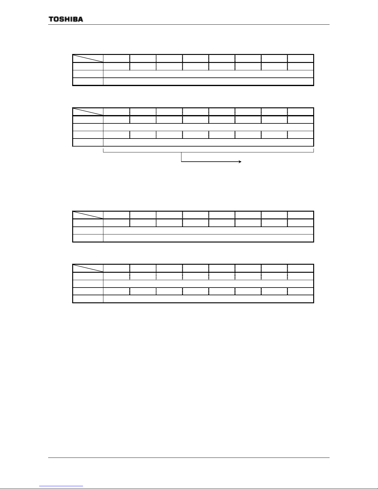
TMP91C824
91C824-57
Port 1 Register
76543210
bit Symbol P17 P16 P15 P14 P13 P12 P11 P10
Read/Write R/W
After Res et Input mode (O utp u t l at ch r eg is ter is cleared t o 0.)
Po rt 1 Control Register
76543210
bit Symbol P17C P16C P15C P14C P13C P 12C P11C P10C
Read/Write W
After Reset00000000
Function 0: IN 1: OUT
Port 2 Register
76543210
bit Symbol P27 P26 P25 P24 P23 P22 P21 P20
Read/Write R/W
After Res et Output latch register is set to “1”
Port 2 Function Regis t er
76543210
bit Symbol P27F P26F P25 F P24F P23F P22F P21F P20F
Read/Write W
After Reset11111111
Function 0: Port 1: Address bus (A23 to A16)
P0
(0000H)
P1
(0001H)
Port 1 I/ O setting
0: Input
1: Output
P1CR
(0004H)
P2FC
(0009H)
(note): Read-modify-write is prohibited for P1CR and P2FC.
P2
(0006H)
Figure 3.5.3 Registers for Ports 1 and 2
Page 61
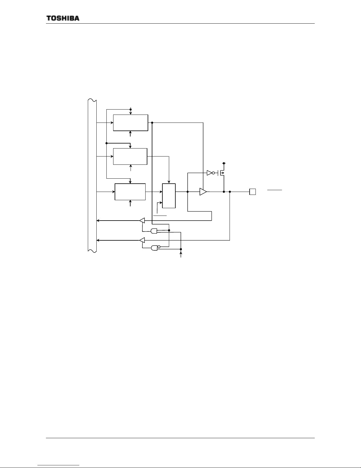
TMP91C824
91C824-58
3.5.3 Port 5 (P54 to P56)
Port 5 is an 5-bit general-purpose I/O port. I/O is set using c o ntrol register P5CR and P5FC. Resetting
resets all bits of the output latch P5 to “1”, the control register P5CR and the function register P5FC to “0”
and sets P54 to P56 to input mode with pull-up register.
In addition to functioning as a general-purpose I/O p ort, Port 5 also functions as I/O for the CPU’s
control / status signal.
Function conrtol
(on bit basis )
S
Output
latch
P55(BUSAK)
Selector
Internal Data BUS
Dire ction control
(on bit basis )
P5CR Write
P-ch
(Programmable
Pull-up)
Reset
P5FC Write
P5 Write
Output buffer
P5 Read
S
A
B
BUSAK
Figure 3.5.4 Port 5 (P55)
Page 62
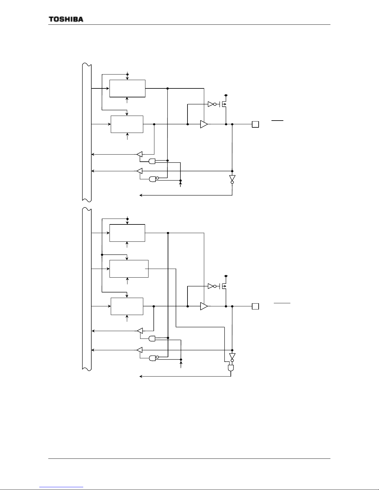
TMP91C824
91C824-59
Internal
WAIT
S
Output
Latch
P5 Write
P5 Read
Internal Data Bus
Dire ction control
(on bit basis )
P5CR Write
P-ch
(Programmable
Pull-up)
Reset
P56 (WAIT)
Function contorol
(on bit basis )
S
Output
Latch
P5FC Write
P5 Write
P54(BUSRQ)
P5 Read
Internal Data Bus
Dire ction control
(on bit basis )
P5CR Write
P-ch
(Programmable
Pull-up)
Reset
Internal
BUSRQ
Output buffer
Figure 3.5.5 Port 5 (P56,P54)
Page 63
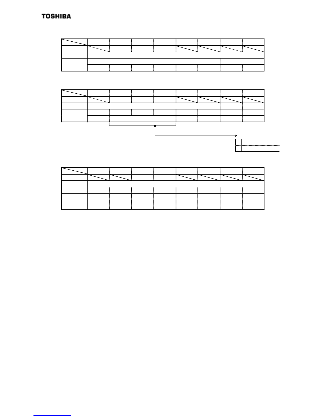
TMP91C824
91C824-60
Port 5 Register
76543210
bit Symb ol P56 P55 P 54
Read/Write R/W
Input mode (With Pull-up)After reset
111
Port 5 Control Regis t er
76543210
bit Symb ol P56C P55C P54C
Read/W rite W
000
After reset
0: IN 1: OUT
Port 5 function register
76543210
bit Symb ol P55F P54F
Read/Write W
After reset 0 0
Function
0: PORT
1: BUSAK
0: PORT
1:BUSRQ
P5FC
(000BH)
P5
(000DH)
II/O setting
0 Input
1Output
(note1): Read-modify-write is prohibited for register P5CR,P5FC.
(note2): When port5 is used in the input mode, P5 register controls the built-in
pull-up resistor. Read-modify-write is prohibited in the input mode or the
I/O mode. Setting the built-in pull- up resistor may be depended on the
States of the input pin.
(note3): When P56 pin is used as a /WAIT pin ,set P5CR<P56C> to “0” and Chip
Select/WAIT control register <BnW2:0> to “010”
P5CR
(000AH)
Figure 3.5.6 Registers for Port 5
Page 64
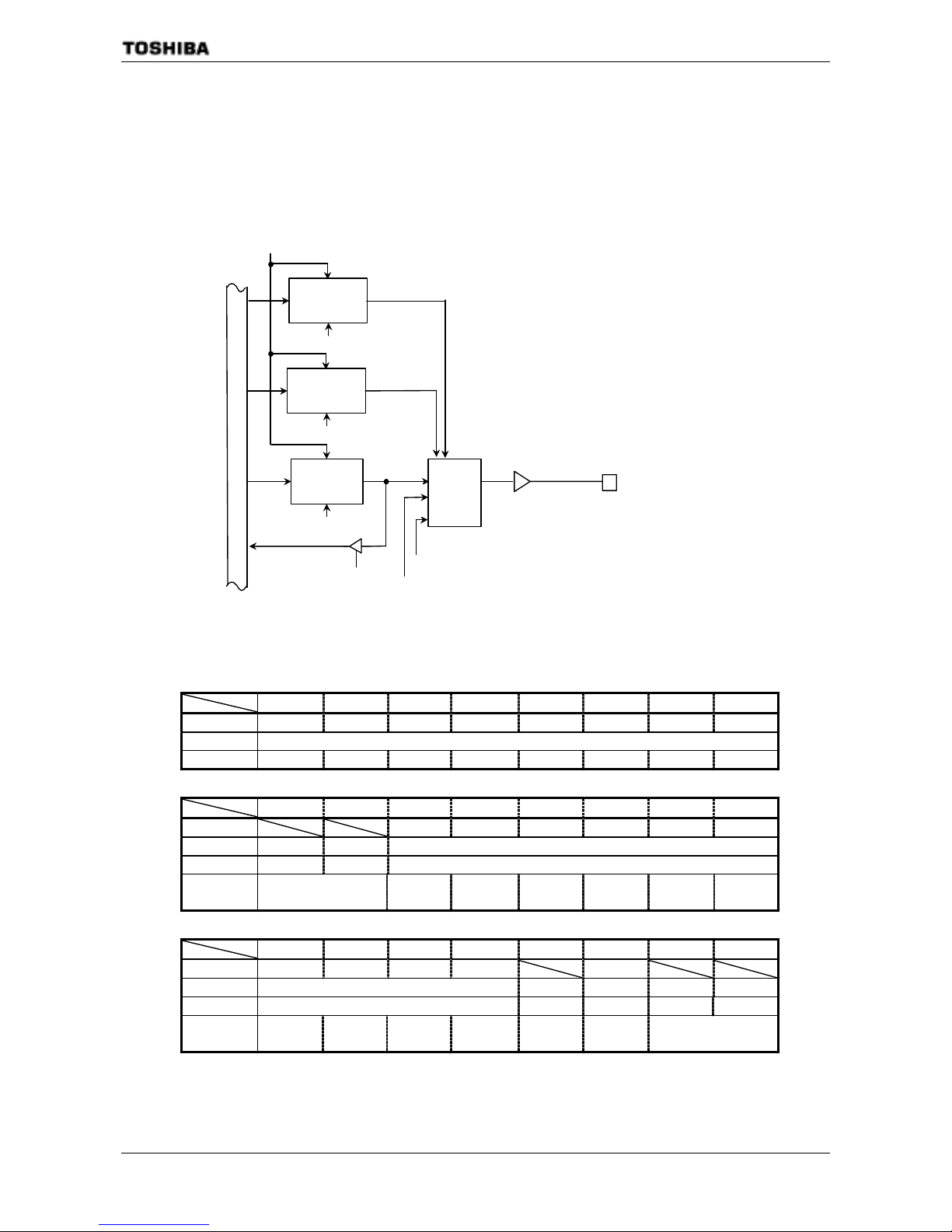
TMP91C824
91C824-61
3.5.4 Port6 (P60 to P67)
Port60 to 67 are 8bit output ports. Resetting sets output latch of P62 to “0” and output latchs of P60 to
P61,P63 to P67 to “1”.
Port6 also function as chip-select output (/CS0 to /CS3), extend address output(EA24).
Writing “1” in the corresponding bit of P6FC, P6FC2 enables the respective functions.
Resetting resets the P6FC, P6FC2 to “0”, and sets all bits to output ports.
Funtion
control
(on bit basis )
Output
lacth
P6 read
Reset
P60 (/CS0),
P61 (/CS1),
P62 (/CS2,/CS2A)
P63 (/CS3),
P64 (EA24,/CS2B)
P65 (EA25,/CS2C)
P66 (/CS2D)
P67 (/CS2E)
/CS0,/CS1,/CS2,/CS3,EA24,EA25
Selector
P6FC write
P6 write
S
A
B
Function
control 2
(on bit basis )
P6FC2 write
“1”,”1”,/CS2A,”1”, /CS2B
C
Figure 3.5.7 Port 6
Port 6 Register
76543210
bit Symb ol P67 P66 P65 P64 P63 P62 P61 P60
Read/Write R/W
After reset 1 1 1 1 1 0 1 1
Port 6 Funct ion R eg is t er
76543210
bit Symbol P65 F P64F P63F P62F P61F P60F
Read/Write W
After reset 0
Function
Always write “0” 0:PORT
1:EA25
0: PORT
1: EA24
0: PORT
1: /CS3
0: PORT
1: /CS2
0: PORT
1: /CS1
0: PORT
1: /CS0
Port 6 Funct i on Register 2
76543210
bit Symb ol P67F2 P66F2 P65F2 P64 F2 P62 F2
Read/Write W W
After reset 0 0
Function
0: <P67F>
1: /CS2E
0: <P66F>
1: /CS2D
0: <P65F>
1: /CS2C
0: <P64F>
1: /CS2B
Always
write “0”
0: <P62F>
1: /CS2A
Always write “0”
P6
(0012H)
P6FC
(0015H)
P6FC2
(001BH)
(note): Read-modify-write is prohibited for P6FC and P6FC2 .
Figure 3.5.8 Register for Port 6
Page 65
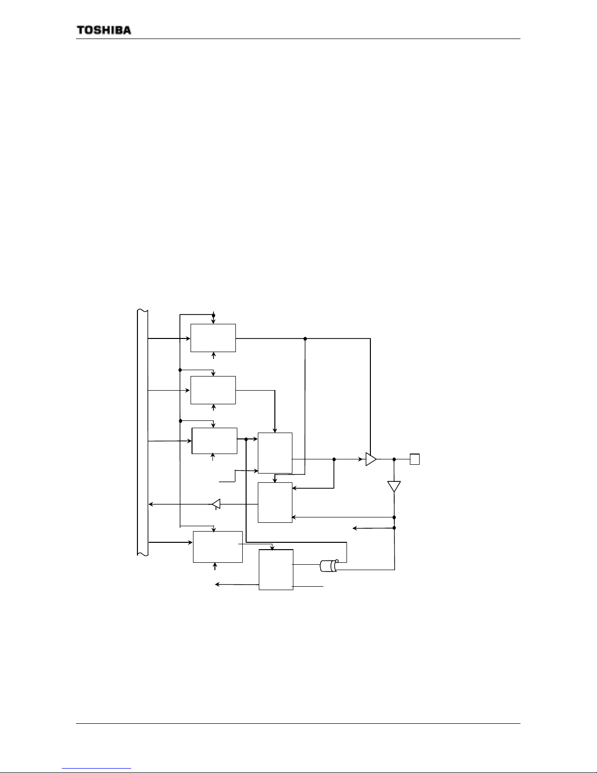
TMP91C824
91C824-62
3.5.5 Port7 (P70 to P77)
Port 7 is an 8-bit general-purpose I/O port. I/O can be set on bit basis using the control register.
Resetting sets Port 7 to input port and all bits of output latch to”1”.
In addition to functioning as a general-purpose I/O port, Port 7 also functions as follows.
1. Input/output function for serial bus interface(SCK,SO/SDA.SI/SCL)
2. Input/output function for IrDA (OPTRX0,OPTTX0)
Writing “1” in the corresponding bit of P7FC, P7FC2 enables the respective functions.
Resetting resets the P7FC, P7FC2 to “0”, and sets all bits to input ports.
(1) Port70 (SCK, OPTRX0)
Port70 is a general-purpose I/O port. It is also used as SCK(clock signal for SIO mode)and
OPTRX0 (receive input for IrDA mode of SIO0).
Used as OPTRX0, it is possible to logical-invert by P7<P70>=”0”.
For PortC1, RXD0 or OPTRX0 is used P7FC2<P70F2>.
Internal data bus
Selector
A
B
S
Selector
A
B
S
P70 (SCK,OPTRX0)
SCK output
P7 read
Direction
control
(on bit basis )
P7CR write
Function
control
(on bit basis )
S
Output latch
P7 write
Reset
P7FC write
SCK input
Function
control2
(onbitbasis)
P7FC2 write
Selector
A
B
S
RXD0
(toSIO0)
RXD0PC1
(fromPORTC1)
logi cal invert
Figure 3.5.9 Port 70
Page 66
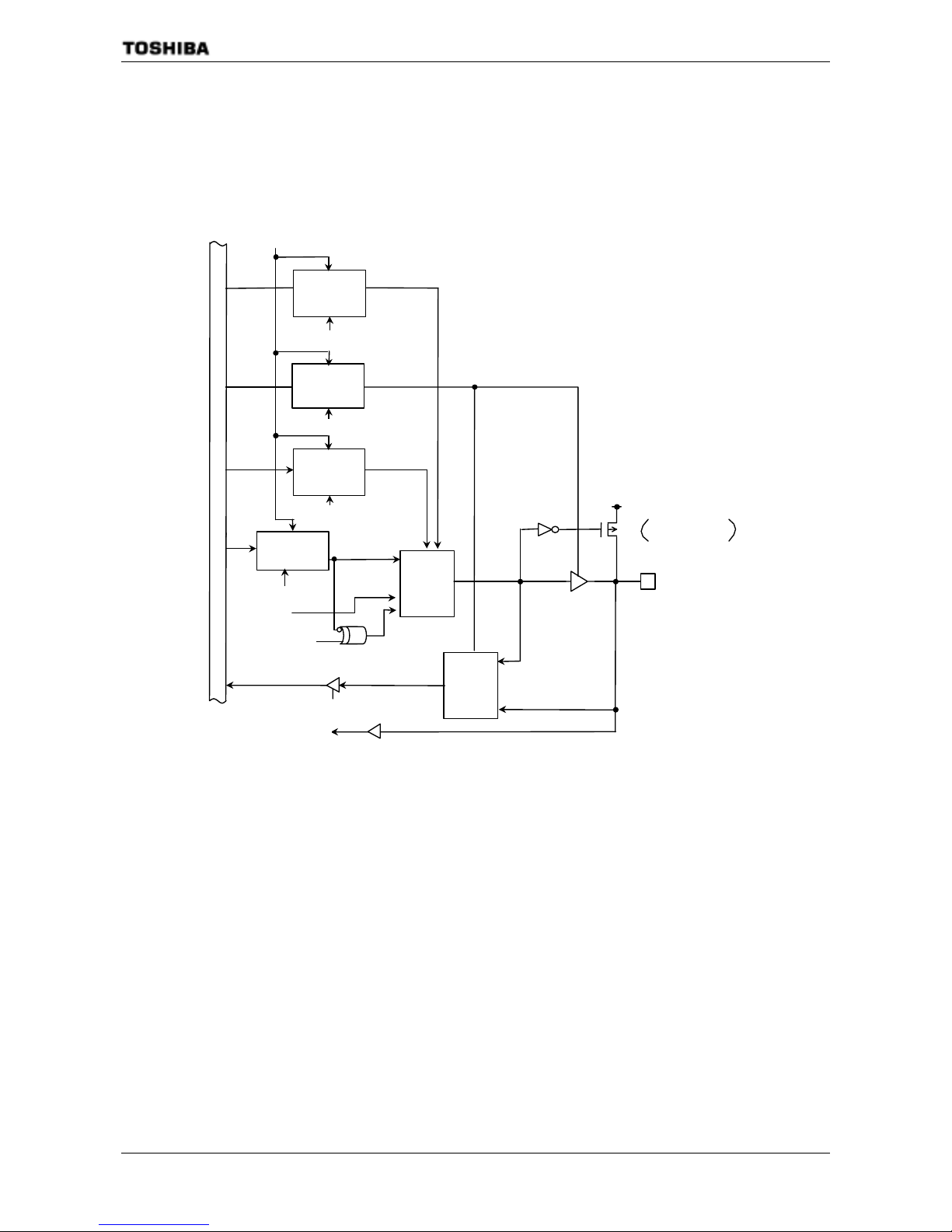
TMP91C824
91C824-63
(2) Port71 (SO/SDA/OPTTX0)
Port71 is a general-purpose I/O port. It is also used as SDA (data input for I
2
C mode), SO (data
output for SIO mode) for serial bus interface and OPTTX0 (transmit output for IrDA mode of
SIO0).
Used as OPTTX0, it is possible to logical-invert by P7<P71>=”0”.
Open drain possible :
P7ODE<ODEP71>
SO output
Internal data bus
Selector
A
B
S
Selector
A
B
S
P71
(SO/SDA,OPTTX0)
P7 read
Direction
control
(on bit basis )
P7CR write
Function
control
(on bit basis )
P7FC write
S
Output latch
P7 write
Reset
SDA input
Programable
pull-up
Function
control 2
(on bit basis )
P7FC2 write
C
logi cal invert
TXD0 outp ut
Figure 3.5.10 Port 71
Page 67
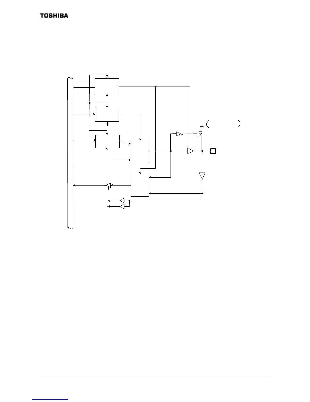
TMP91C824
91C824-64
(3) Port 72 (SI/SCL,/HRESET)
Port72 is a general-purpose I/O port. It is also used as SI (data input for SIO mode), SCL (clock
input/output for I
2
C mode) for serial bus interface and input for release hard-protect.
Open drain possible :
P7ODE<ODEP72>
SCL outpu t
Internal data bus
Selector
A
B
S
Selector
A
B
S
P72 (SI/SCL)
P7 read
Direction
control
(on bit basis )
P7CR write
Function
control
(on bit basis )
P7FC write
S
Output latch
P7 write
Reset
SI input
SCL input
P-ch
Programable
Pull-up
Figure 3.5.11 Port 72
Page 68
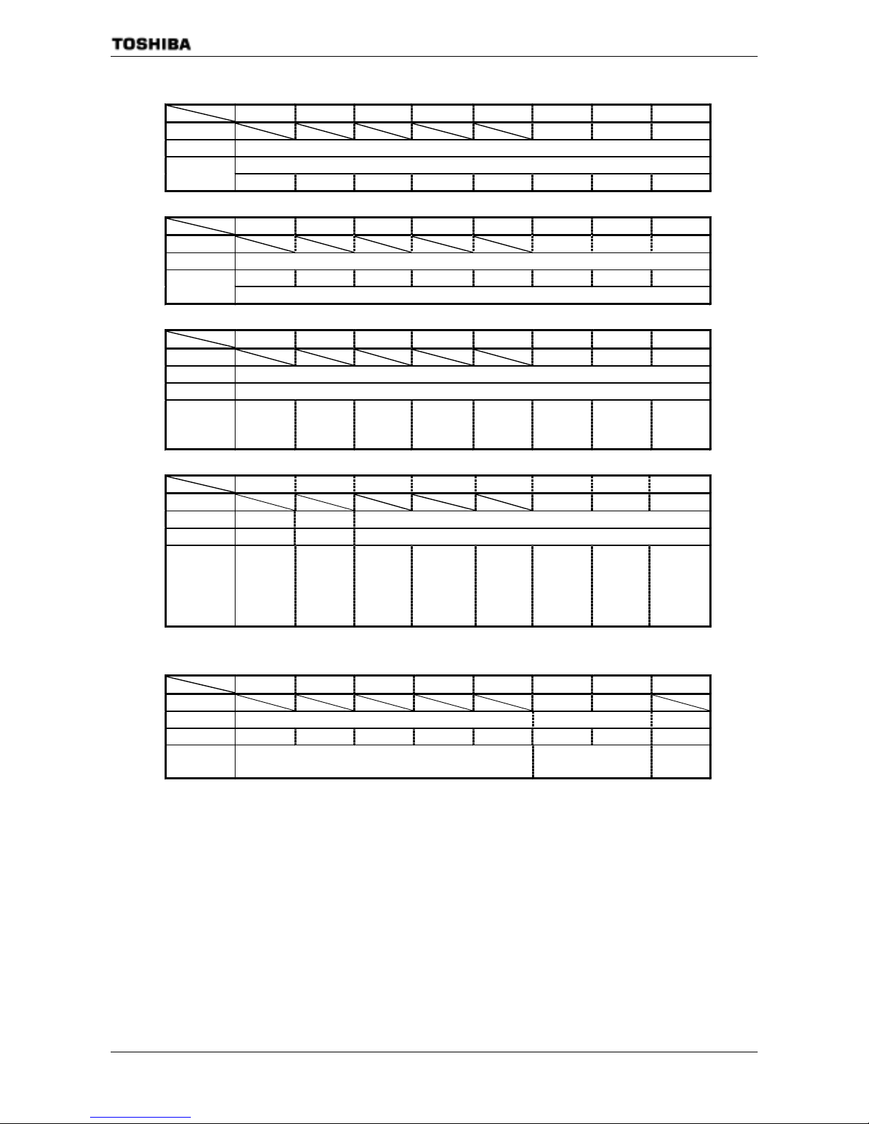
TMP91C824
91C824-65
Port 7 Register
76543210
bit Symb ol P72 P71 P 70
Read/Write R/W
Input mode
After reset
111
Port 7 Control Register
76543210
bit Symb ol P72C P71C P 70C
Read/Write W
000
After reset
0: IN
1: OUT
Port 7 Funct ion R eg is ter
76543210
bit Symbol P72F P71 F P70F
Read/Write W
After reset 0
Function
0: PORT
1: SCL
output
0: PORT
1:
SDA/SO
output
0: PORT
1: SCK
output
Port 7 Funct i on R eg ister 2
76543210
bit Symb ol P72F2 P71F2 P70 F2
Read/Write W
After reset 0
Function
Always write
to ‘0’
0: <P71F>
1: OPTTX0
SIO0 RXD
Pin select
0: RXD0(PC1)
1:OPTRX0
(P70)
P7FC
(0017H)
P7
(0013H)
P7CR
(0016H)
P7FC2
(001CH)
Port 7 ODE Register
76543210
bit Symbol ODEP72 ODEP71
Read/Write
After reset 0 0
Function
0: 3-STATE
1: Open Drain
P7ODE
(001FH)
(note): Read-modify-write is prohibited for P7CR,P7FC, P7FC2 and P7ODE.
Figure 3.5.12 Register for Port 7
Page 69
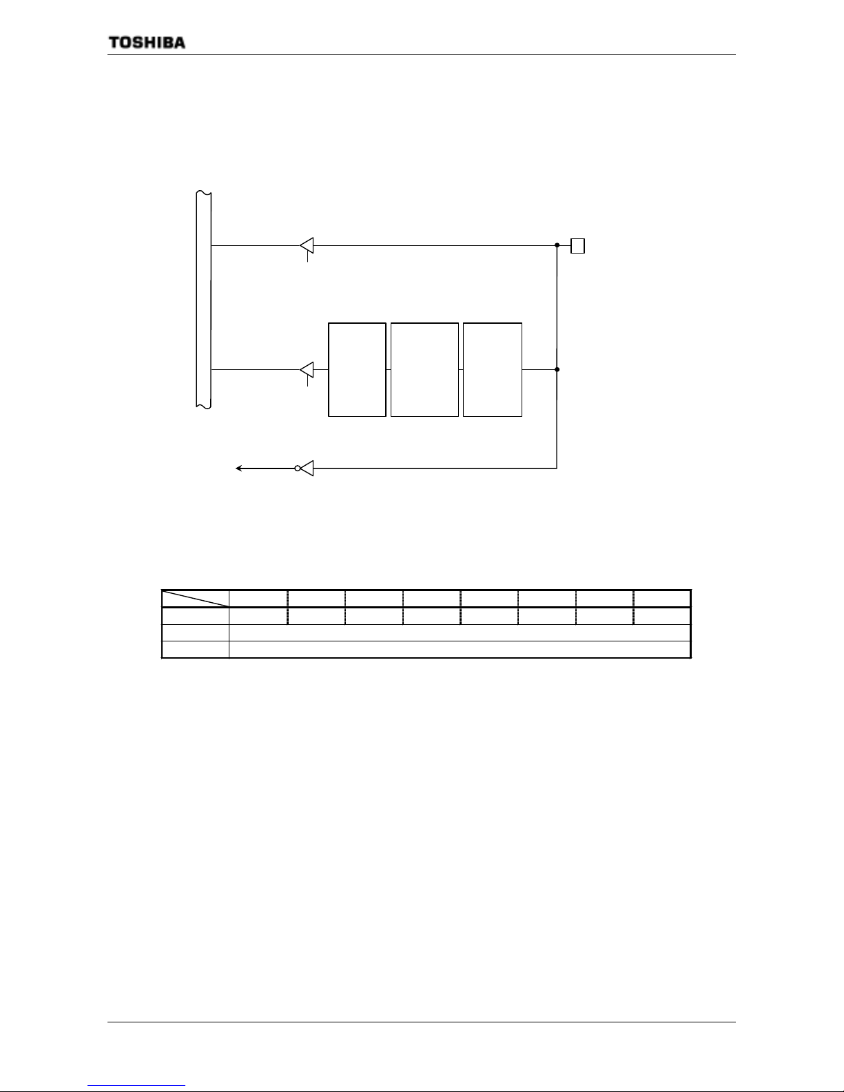
TMP91C824
91C824-66
3.5.6 Port 8 (P80 to P87)
Port 8 is an 8-bit input port and can also be used as the analog input pins for the internal A/D converter.
P83 can also be used as ADTRG pin for the A/D converter.
Internal da t a bus
AD Read
Conversion
Result
Register
A/D
Converter
Channel
Selector
Port 8 read
Port 8
P80 to P87
(AN0 to AN7)
A
DTRG
(for P83 only)
Figure 3.5.13 Port 8
Port 8 Register
76543210
Bit Symbol P87 P86 P85 P84 P83 P82 P81 P80
Read/Write R
After reset Input mode
(note): The inp ut ch an nel select i on of A/D Converter and th e p er mis s ion of ADTR G inp ut are set by A/D Convert er
mode register ADMOD1.
P8
(0018H)
Figure 3.5.14 Register for Port 8
Page 70
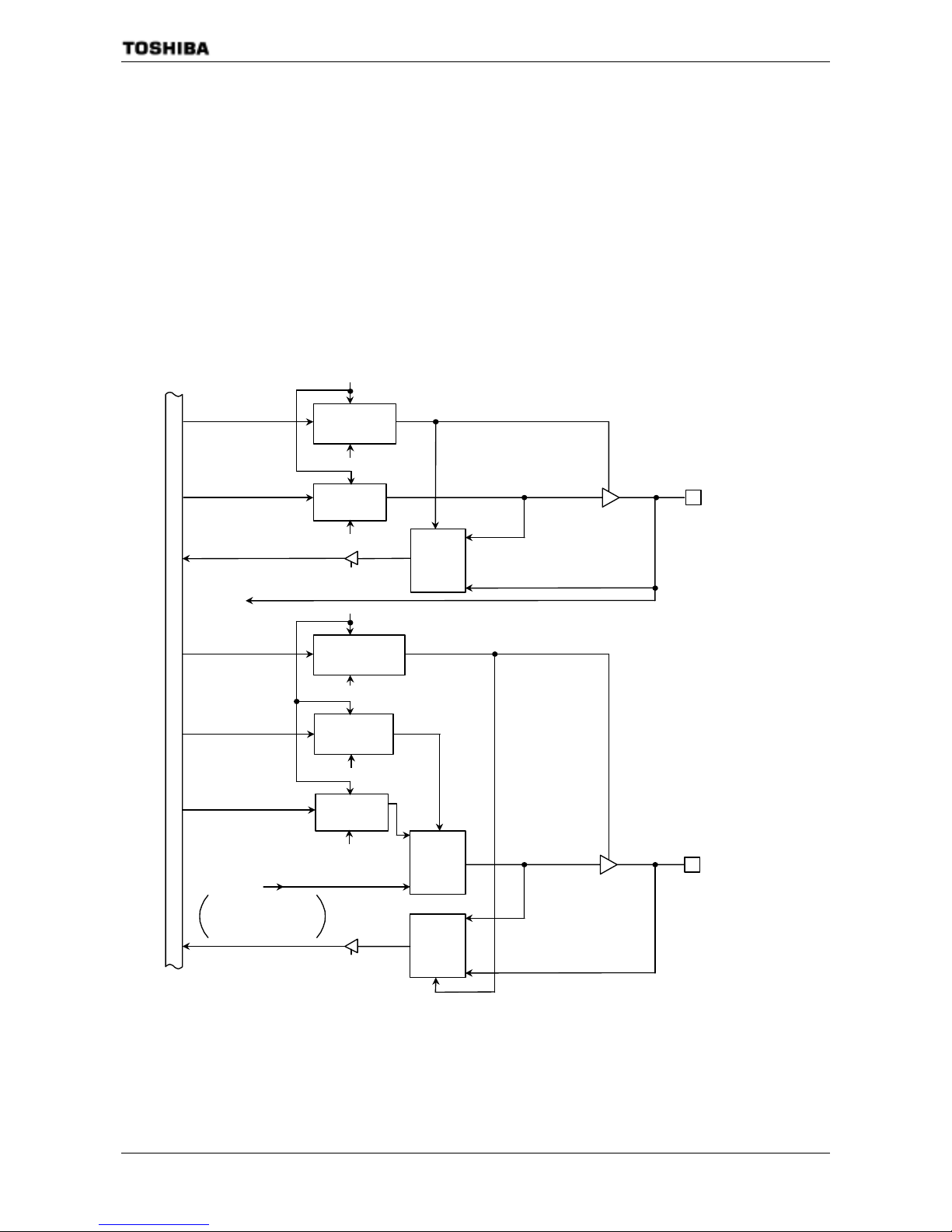
TMP91C824
91C824-67
Port B (PB0 to PB6)
Port B0 to PB6 is a 7-bit general-purpose I/O port. Each bi t can be s et in di v i dual ly for i n put or ou t pu t .
Resetting sets Port B to be an input port.
In addition to functioning as a general -purpose I/O p ort, P ort B0 has clock input ter minal TA0IN of 8
bits timer 0, and port B1, B2 each has facility of 8 bits timer listing TA1OUT, TA3OUT terminal. And,
port B3 to B6 has each external interruption input facility of INT0 to INT3. Edge selection of external
interruption is establishes by IIMC register in the interrupt controller.
Timer output function and external interrupt function can be enabled by writing “1” to the
corresponding bits in the Port B Function Register (PBFC). Resetting resets all bits of the registers PBCR
and PBFC to “0”, and sets all bits to be input ports.
(1) PB0 to PB2
TA0IN
PB1 (TA1OUT)
PB2 (TA3OUT)
PB read
Timer F/F OUT
PB read
Internal data bus
Selector
A
B
S
Selector
ABS
Selector
A
B
S
PB0 (TA0IN)
Direction Control
(on bits basis)
S
Output latch
PBCR write
PB write
Direction Control
(on bits basis)
PBCR Write
Function control
(on bits basis)
PBFC Write
S
Output latch
PB Write
Reset
TA1OU T : Timer A1
TA3OU T : Timer A3
Reset
Figure 3.5.15 Port B0 to B2
Page 71
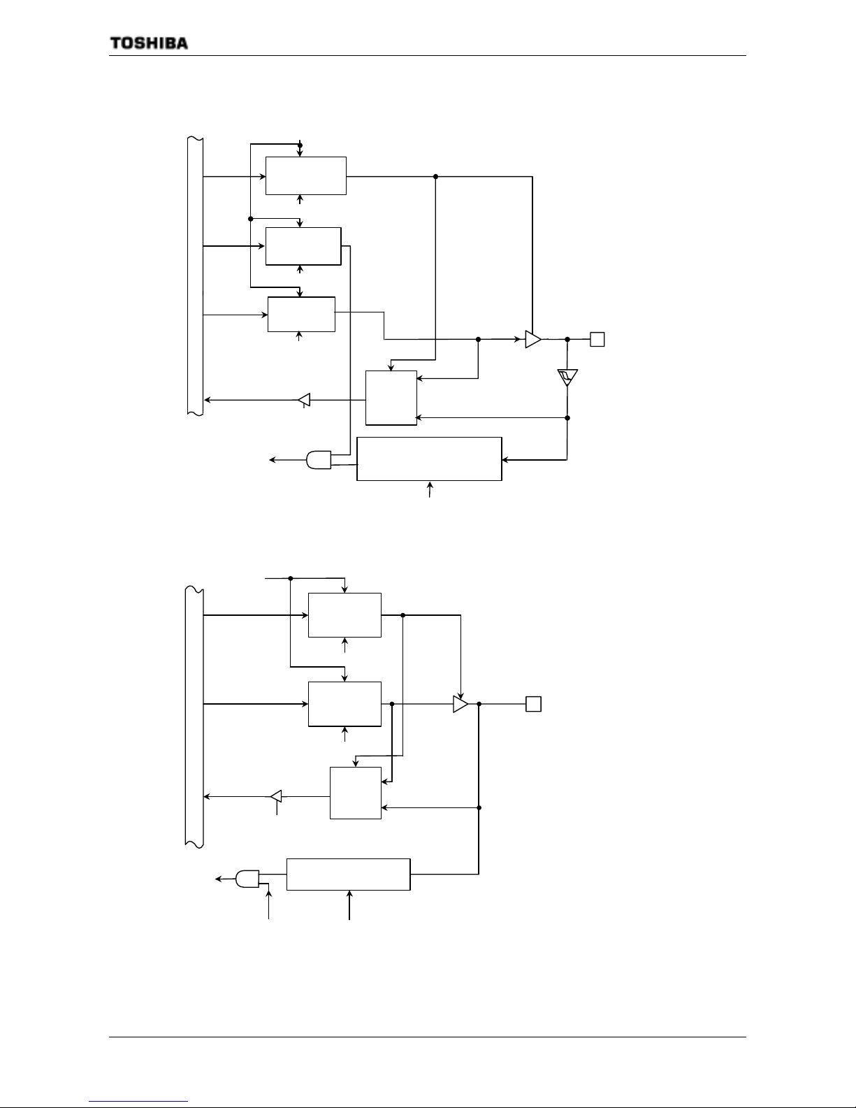
TMP91C824
91C824-68
(2) PB3 (INT0), PB4 (INT1)-PB6 (INT3)
Internaldatabus
Selector
A
B
S
PB3 (INT0)
PB read
Direction Control
(on bits basis)
PBCR write
Function control
(on bits basis)
S
Output latch
PB write
Reset
PBFC write
Level / edge select
&
Raising/Falling select
INT0
IIMC<I0LE, I0EDGE>
Figure 3.5.16 Port B3
Direction Control
(on bits basis)
Reset
PBCR write
S
Out latch
PB write
PB4∼PB6
(INT1
∼
INT3)
Selector
PB read
Raising/Falling
edge-detection
PAFC< PA4F,
PA5F,
PA6F>
IIMC< I1EDGE,
I2EDGE,
I3EDGE >
S
B
A
Y
INT1
INT3
to
Figure 3.5.17 Port B4 to B6
Page 72
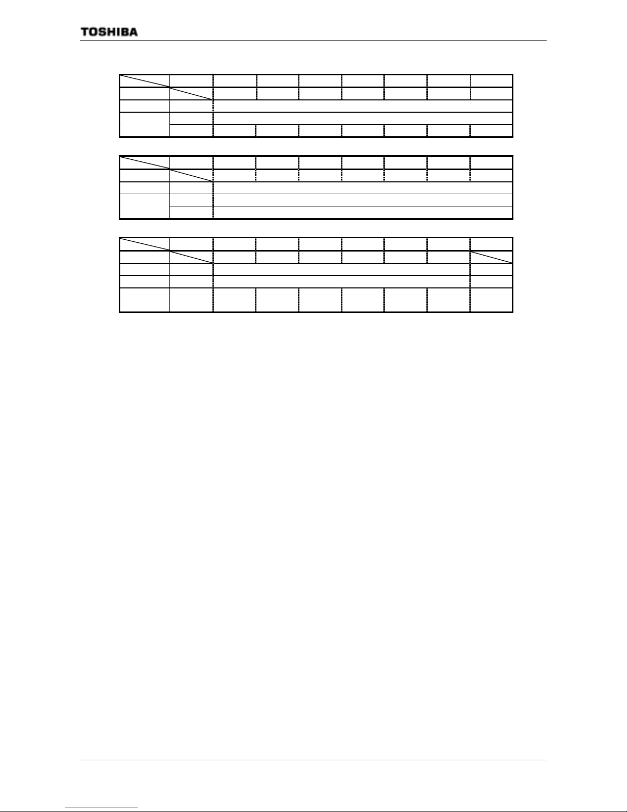
TMP91C824
91C824-69
Port B Regist er
76543210
bit Symbol PB6 PB5 PB4 PB3 PB2 PB1 PB0
Read/Write R/W
Input ModeAfter Reset
1111111
Port B Control Register
76543210
bit Symbol PB6C PB5C PB4C PB3C PB2C PB1C PB0C
Read/Write W
0After Reset
0: IN
1: OUT
Port B Function Register
76543210
bit Symbol PB6F PB5F PB4F PB3F PB2F PB1F
Read/Write W
After Reset 0
Function
0: PORT
1: INT3
0: PORT
1: INT2
0: PORT
1:
INT1
0: PORT
1: INT0
0: PORT
1:
TA3OUT
0: PORT
1:
TA1OUT
PBFC
(0025H)
PB
(0022H)
PBCR
(0024H)
(note1): Read-Modify-Write is prohibited for the registers PBCR and PBFC.
(note2): PB0/TA0IN pin does not have a register changing PORT/FUNCTION.
F or ex am pl e, w h en it is us ed as an inp ut port, the inp ut sig n al is in putted to
8 bit timer.
Figure 3.5.18 Register for Port B
Page 73
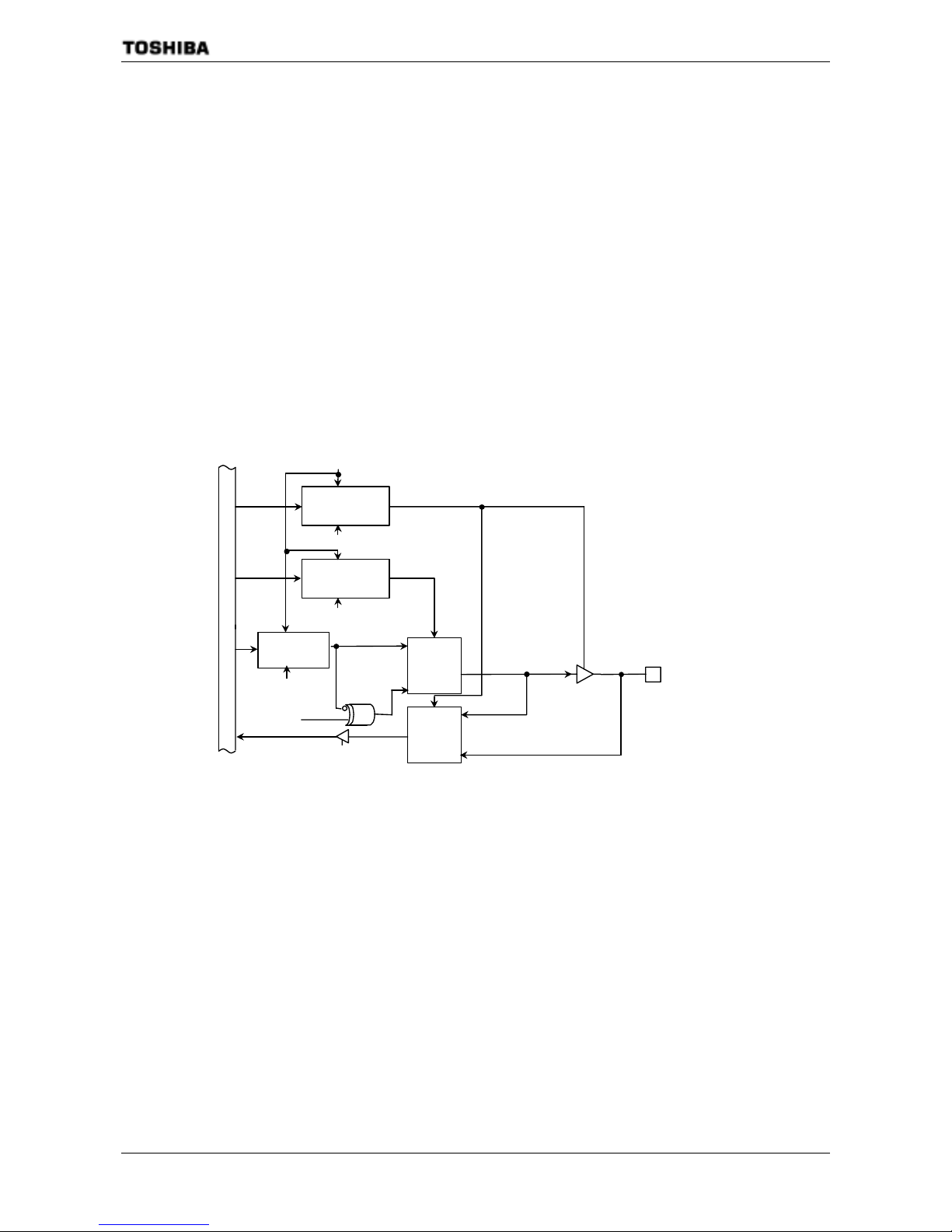
TMP91C824
91C824-70
3.5.7 Port C (PC0 to PC5)
Port C0 to C5 are 6-bit general-purpose I/O ports. Each bit can be set individually for input or
output. Resetting sets PC0 to PC5 to be an input ports. It also sets all bits of the output latch register
to “1”.
In addition to functioning as general-purpose I/O port pins, PC0 to PC5 can also function as the I/O
for serial channels 0 and 1. A pin can be enabled for I/O by writing “1 ” to the corresponding bit of
the Port C Function Register (PCFC).
Resetting resets all bits of the registers PCCR and PCFC to 0 and sets all pins to b e input ports .
(1) Port C0, C3 (TXD0/TXD1)
As well as functioning as I/O port pins, port C0 and C3 can also function as serial channel T XD
output pins. In case of use TXD0/TXD1, it is possible to logical invert by setting the register
PC<PC0,PC3>.
And port C0 to C3 have a programmable open drain function which can be controled by the
register PCODE<ODEPC0, ODEPC3>.
PCODE<ODEPC0, C3>
Open-drain
set possible
Selector
ABS
Selector
A
BS
PC0 (TXD0)
PC3 (TXD1)
TXD0, TXD1
PC Read
Ditection control
(On bit basis)
PCCR write
Function control
(On bit basis)
PCFC write
S
Output latch
PC write
Reset
Internal da t a bus
Logical invert
Figure 3.5.19 Port C0 and C3
Page 74
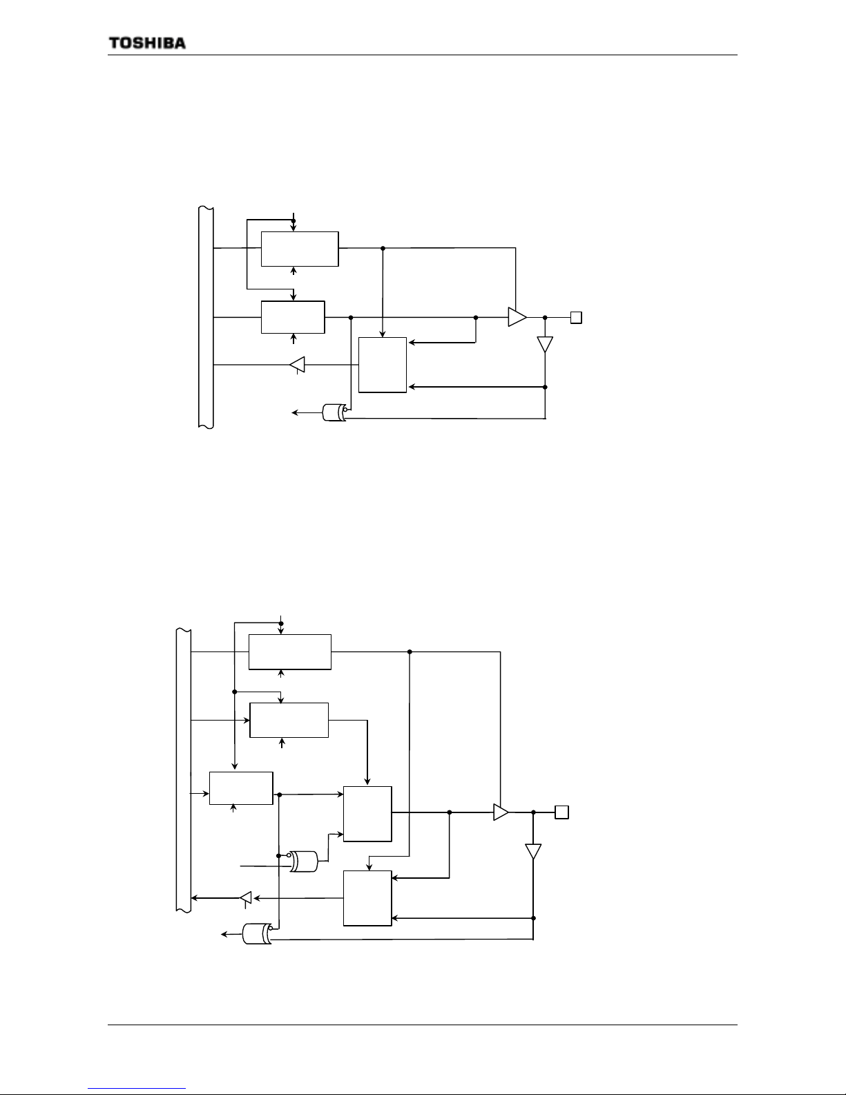
TMP91C824
91C824-71
(2) Port C1, C4 (RXD0, 1)
Port C1 and C4 are I/O port pins and can also is us ed as RXD input for th e serial channels. In case
of use RXD0/RXD1, it is possible to logical invert by setting the register PC<PC1,PC4>.
And input data of SIO0 can be select from RXD/ PC 1 pin or OPTRX0/ P70 by setting the register
PCFC2<P70F2>.
RXD0PC1,
RXD1
Selector
A
BS
PC read
PC1 (RXD0)
PC4 (RXD1)
Ditection control
(On bit basis)
PCCR write
Reset
S
Output latch
Internal da t a bus
PC write
Logical invert
Figure 3.5.20 Port C1 and C4
(3) Port C2(/CTS0,SCLK0),C5( /CST1,SCLK1)
Port C2 and C4 are I/O port pins and can also is used as /CTS input or SCLK input/output for the
serial channels. In case of use /CTS,SCLK, it is possible to logical invert by setting the register
PC<PC2,PC5>.
Selector
ABS
Selector
A
BS
PC2 (SCLK0,/CTS0)
PC5 (SCLK1,/CTS1)
SCLK0, 1
outpu
t
PC read
Ditection control
(On bit basis)
PCCR write
Function control
(On bit basis)
PCFC write
S
Output latch
PC write
Reset
/CTS0,1
SCLK0, 1
input
Interna l da ta bus
Logical
invert
Logical invert
Figure 3.5.21 Port C2 and C5
Page 75
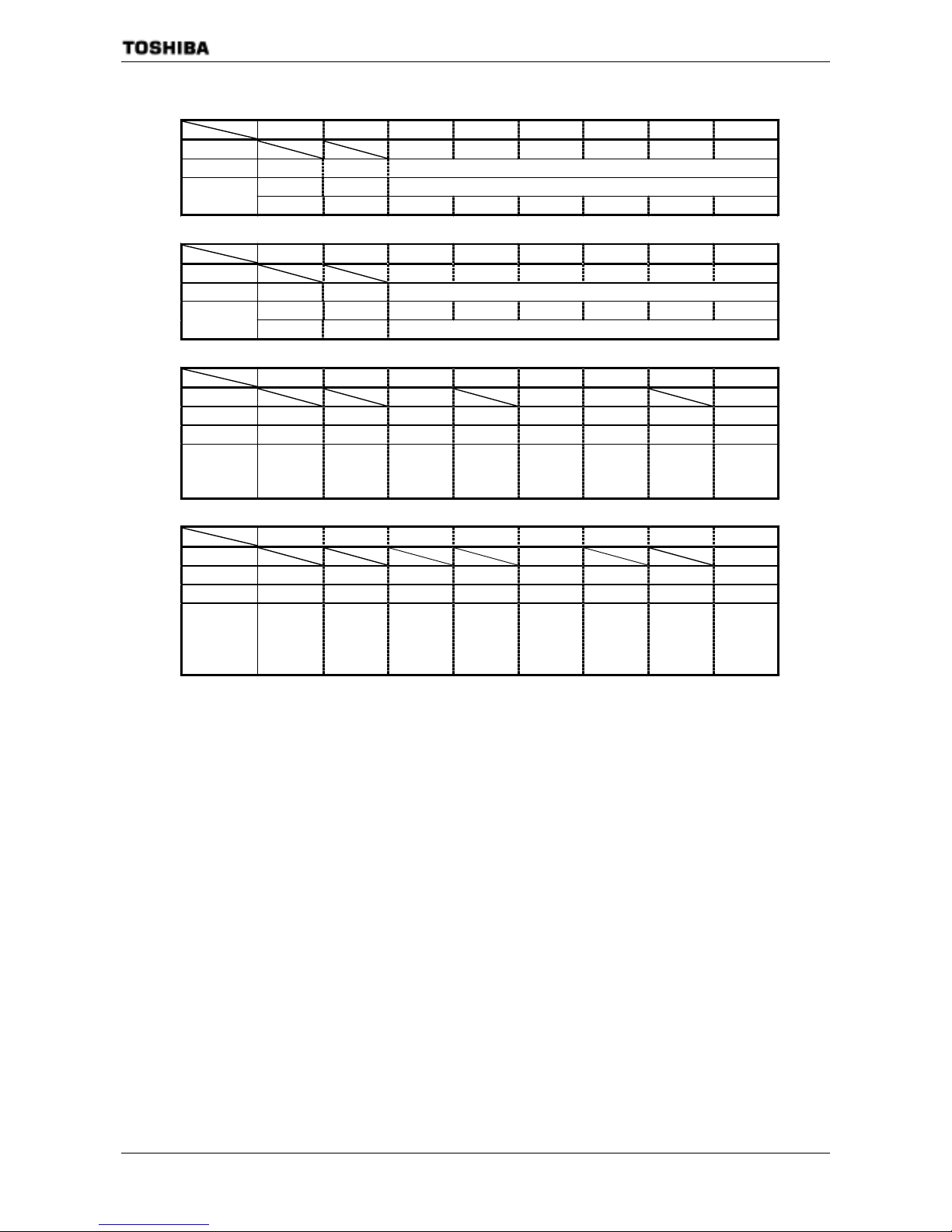
TMP91C824
91C824-72
Port C Register
76543210
bit Symbol PC5 PC4 PC3 PC2 PC1 PC0
Read/Write R/W
Input modeAfter Reset
111111
Port C Cont rol Register
76543210
bit Symb ol PC5C PC4C PC 3C PC2C PC1C PC0C
Read/Write W
000000After Reset
0: IN
1: OUT
Port C Functon Register
76543210
bit Symb ol PC5F PC3F PC2F PC0F
Read/Write W W W W
After Reset 0 0 0 0
Function
0: PORT
1:
SCLK1
Output
0: PORT
1:
TXD1
0: PORT
1:
SCLK0
Out put
0: PORT
1:
TXD0
Port C ODE Register
76543210
bit Symbol ODEPC3 ODEPC0
Read/Write W W
After Reset 0 0
Function
TXD1
0: CMOS
1:
Open
Drain
TXD0
0: CMOS
1:
Open
Drain
PCFC
(0027H)
PC
(0023H)
PCCR
(0026H)
PCODE
(0028H)
(note1): Read-Modify-Write is prohibited for the registers PCCR, PCFC and PCODE.
(note2): PC1/RXD0, PC4/RXD1 pins do not have a register changing PORT/FUNCTION. For example,
when it is used as an input port, the input signal is inputted to SIO as the cereal receive data.
Figure 3.5.22 Register for Port C
Page 76
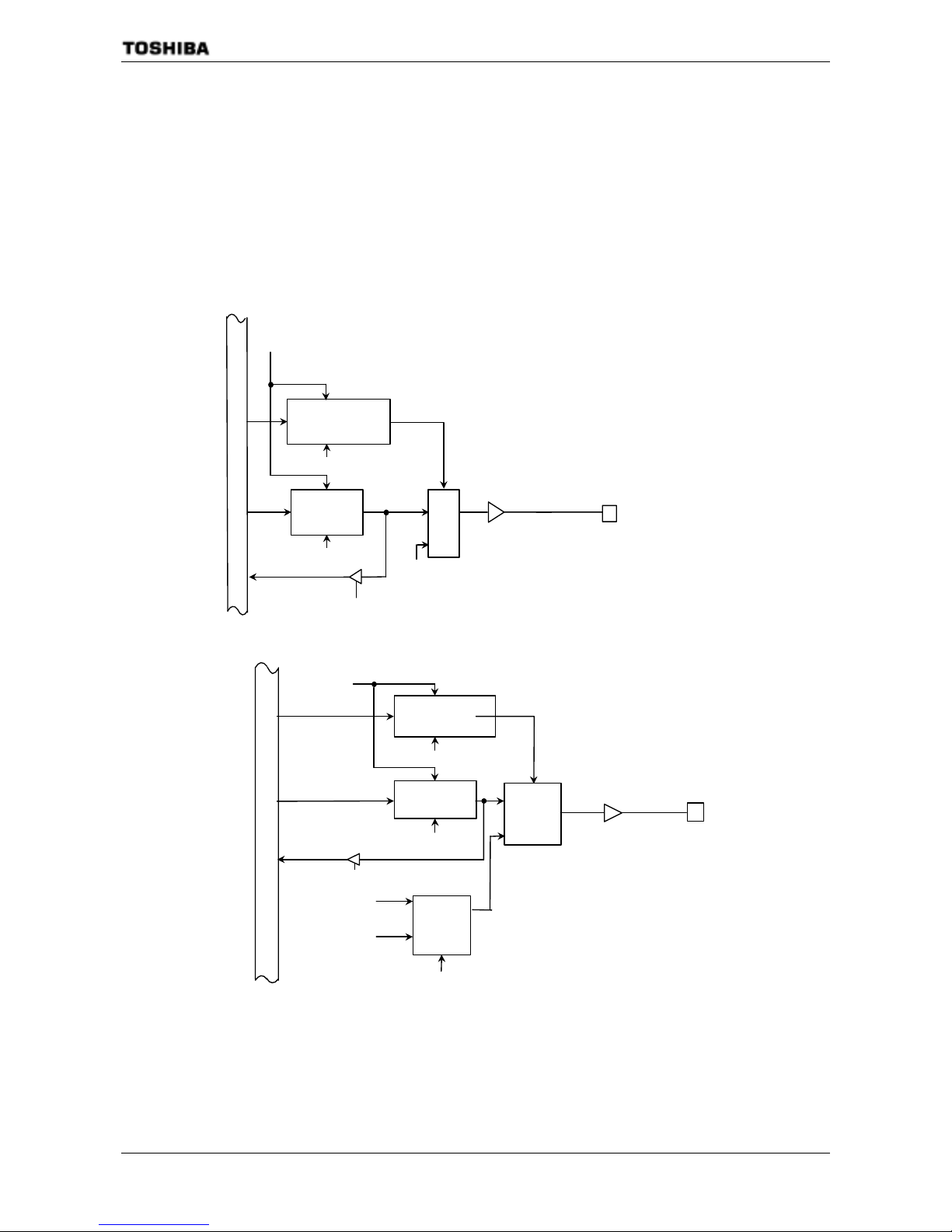
TMP91C824
91C824-73
3.5.8 Port D (PD0 to PD7)
Port D is an 8-bit output port. Resetting sets the output latch PD to “1”, and PD5 to PD7 pin output “1”.
In addition to functioning as output p or t, Po rt D also f unction as o utp ut pin for output pin for inter nal
clock (SCOUT), output pin for RTC alarm (/ALARM) and output pin for melody/alarm generator
(MLDALM,/MLDALM). Above setting is used the function register PDFC.
Only PD6 has two output functions which /ALARM and /MLDALM. This selection is used PD<PD6>.
Resetting resets the function register PDFC to “0”, and sets all ports to output ports.
Function control
(On bit basis)
Output latch
PD read
Reset
PD7(MLDALM)
MLDALM
Output buf f er
Selector
PDFC write
PD write
S
A
B
Internal data bus
Figure 3.5.23 Port D
Internal data bus
Fs clock
Reset
S
Output latch
PD write
PD read
Function control
(On bit basis)
PDFC write
S
A
Y
Selector
B
f
SYS
clock
SYSCR2<SCOSEL>
PD5 (SCOUT)
A
Y
Selector
B
S
Figure 3.5.24 Port D
Page 77
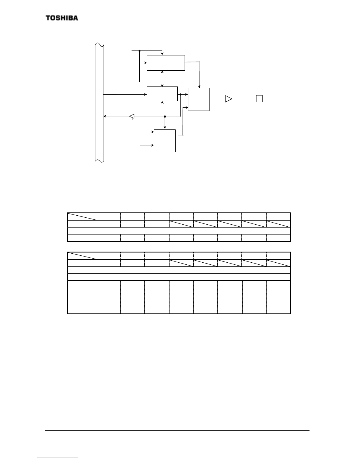
TMP91C824
91C824-74
Internal data bus
/MLDALM
Reset
S
Output latch
PD write
PD read
Function control
(On bit basis)
PDFC write
S
A
Y
Selector
B
/ALARM
PD6 (/ALARM,
/MLDALM)
A
S
Y
Selector
B
Figure 3.5.25 Port D
Port D register
76543210
bit Symb ol PD 7 PD6 P D5
Read/Write R/W
After Reset 1 1 1
Port D function register
76543210
bit Symb ol PD7F PD6F PD5F
Read/Write W
After Reset 0
Function
0: PORT
1: MLDALM
0: PORT
1: /ALARM
@<PD6>=1
1: /MLDALM
@<PD6>=0
0: PORT
1: SCOUT
PD
(0029H)
PDFC
(002AH)
(note): Read-Modify-Write is prohibited for the registers PDFC.
Figure 3.5.26 Register for Port D
Page 78

TMP91C824
91C824-75
3.5.9 Port Z(PZ2 to PZ3)
Port Z is the 2-bit general-purpose I/O port. I/O is set using control register PZCR and PZFC. Resetting
resets all bits of the output latch PZ to “1”.
In addition to functioning as a ge neral-purpose I/O port, Port Z also functio ns as I/O for the CPU’s
control / status signal.
Resetting initializes PZ2 and PZ3 pins to input mode with pull-up register.
When the PZ<RDE> register clearing to “0”,outputs the R D strobe (used for the peu sed static RA M) of
the RD pin even when the internal addressed.
If the <RDE> remains “1”, the RD strobe signal is output only when the external address are is
accessed.
Page 79
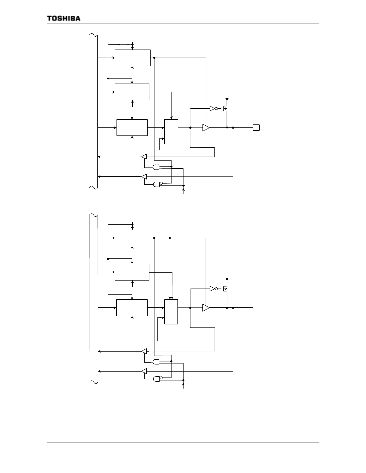
TMP91C824
91C824-76
Function conrtol
(on bit basis)
S
Output
latch
PZ2(/HWR)
Selector
Internal Data BUS
Direction control
(on bit basis)
PZCR Writ e
P-ch
(Programmable
Pull-up)
Reset
PZFC Write
PZ Write
Output buffer
PZ Read
S
A
B
/WHR
Function conrtol
(on bit basis )
S
Output
latch
PZ3(R/W)
Selector
Internal Data BUS
Dire ction control
(on bit basis )
PZCR Write
P-ch
(Programmable
Pull-up)
Reset
PZFC Write
PZ Write
Output buffer
PZ Read
S
A
B
R/W
Figure 3.5.27 Port Z (PZ2,PZ3)
Page 80
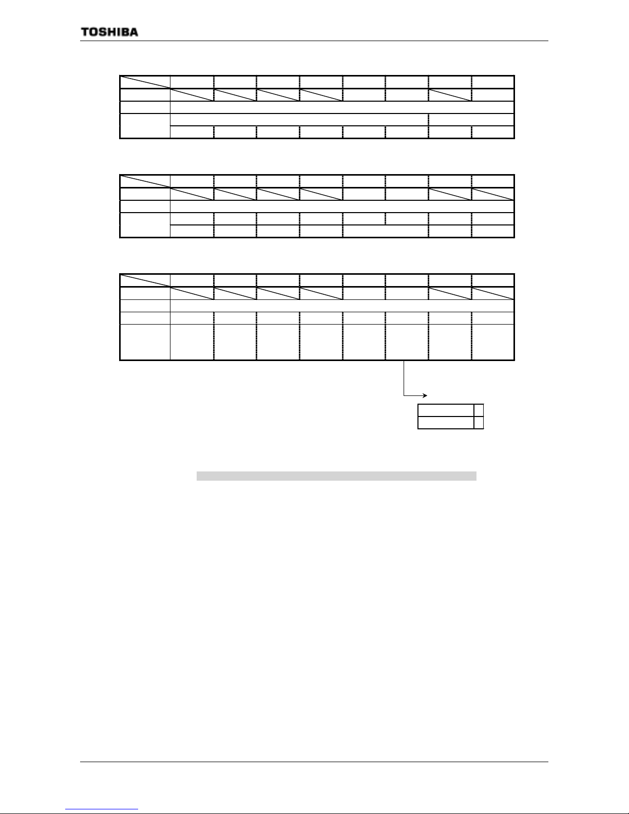
TMP91C824
91C824-77
Port Z Register
76543210
bit Symb ol PZ3 PZ2 RDE
Read/Write R/W
Input mode (pulled-up)
After reset
11 1
Port Z Control Register
76543210
bit Symb ol PZ3C PZ2C
Read/Write W
00
After reset
0: IN 1: OUT
Port Z Function Register
76543210
Bit Symbol PZ3F PZ2F
Read/Write W
After reset 0 0
Function
(Note)
Always
fixed to “0”
0: PORT
1: R/W
0: PORT
1:/HWR
PZFC
(007FH)
PZ
(007DH)
Note 1: Read-Modify-write is prohibited for registers PZCR and PZFC.
Note 2: When Port Z is used in Input Mode, the PZ register controls the built-in pull-up resistor. Read-Modify-Write is prohibited in
Input Mode or I/O Mode.
Setting the built-in pull-up resistor may be depended on the states of the input pin.
/HWR setting
PZFC<PZ2F> 1
PZCR<PZ2C> 1
PZCR
(007EH)
Figure 3.5.28 Port Register for Port Z
Page 81

TMP91C824
91C824-78
3.6 Chip Select/Wait Controller
On the TM91C824, four user-speci f iabl e addres s areas (C S0 to CS 3) can be se t. The data bus width and th e
number of waits can be set independently for each address area (CS0 to CS3 and others).
The pins /CS0 to /CS3 (which can also function as port pins P60 to P63) are the respective output pins for the
areas CS0 to CS3. When the CPU specifies an address in one of these areas, the corresponding /CS0 to /CS3
pin outputs the Chip Select signal for the specified address area (in R OM or SRAM). However, in order for th e
Chip Select signal to be output, the Port 6 Function Register P6FC must be set.
/CS2A to /CS2E (CS pin except /CS0 to /CS3) are made by MMU.
These pins is /CS pin that area and BANK value is fixed without concern in setting of CS/WAIT controller.
The areas CS0 to CS3 are defin ed by the values in the Memory Start Address Registers MSAR0 to MSAR3
and the Memory Address Mask Registers MAMR0 to MAMR3.
The Chip Select/Wait Control Registers B0 CS to B3CS and BEXCS should be used to specify the Master
Enable/Disable status the data bus width and the number of waits for each address area.
The input pin controlling these states is the bus wait request pin (WAIT).
3.6.1 Speci fying an Address Area
The CS0 to CS3 address areas are specified using the start address registers (MSAR0 to MSAR3) and
memory address mask registers (M AMR0 to MAMR3).
At each bus cycle, a compare operation is performed to determine if the address on the specified a
location in the CS0 to CS3 area. If the result of the comparison is a match, this indicates an access to the
corresponding CS area. In this case, the /CS0 to /CS3 pin outputs the chip select signal and the bus cycle
operates in accordance with the settings in chip select/wait control register B0CS to B3CS. (See 3.6.2,
Chip Select/Wait Control Registers.)
Page 82
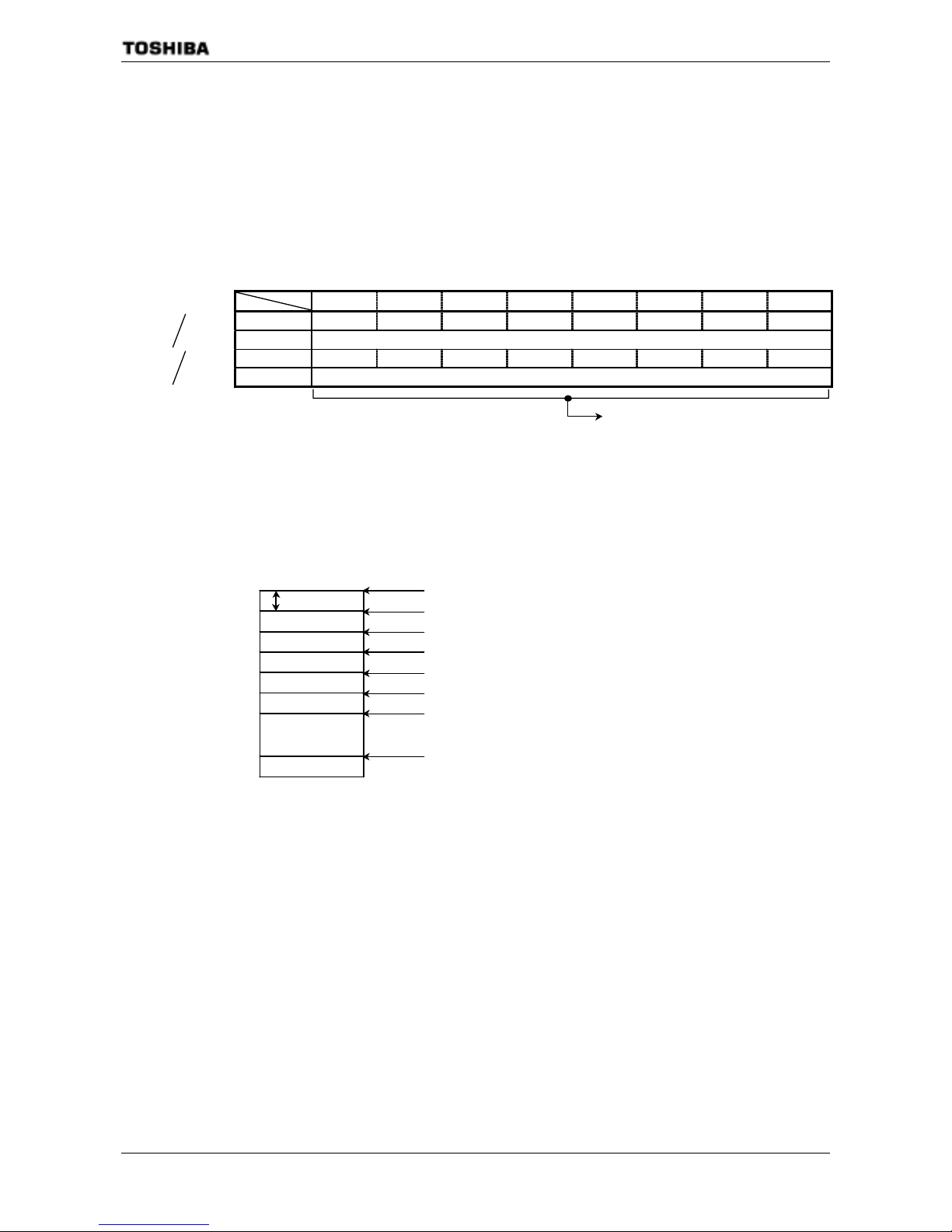
TMP91C824
91C824-79
(1) Memory Start Address Registers
Figure 3.6.1 sho ws the Memory Start Add ress Registers. T he Memory Start Address Registers
MSAR0 to MSAR3 set the start addresses for the CS0 to CS3 areas. Set the upper eight bits (A23 to
A16) of the start address in <S23: S16>. The lower 16 bits of the start address (A15 to A0) are
permanently set to 0. Accordingly, the start address can only be set in 64-Kbyte increments, starting
from 000000H. Figure 3.6.2 sho ws the relationship between the start address and the start address
register value .
Memo ry Sta rt Add ress Reg i st ers (fo r areas CS0 to CS3)
76543210
bit Symbol S23 S22 S21 S20 S19 S18 S17 S16
Read/Write R/W
After reset11111111
Function Determines A23 to A16 of start address.
MSAR0
(00C8H)
MSAR1
(00CAH)
MSAR2
(00CCH)
MSAR3
(00CEH)
Set s start add re sse s for a reas CS0 to CS3.
Figure 3.6.1 Memory Start Address Register
64K byt es
Address
000000H
FFFFFFH
000000H
・・・・・・・・・・・
00H
010000H ・・・・・・・・・・・ 01H
020000H ・・・・・・・・・・・ 02H
030000H ・・・・・・・・・・・ 03H
040000H ・・・・・・・・・・・ 04H
050000H ・・・・・・・・・・・ 05H
060000H ・・・・・・・・・・・ 06H
FF0000H
・・・・・・・・・・・
FFH
St art address Value in sta rt add re ss regi st er (M S A R0 t o M SAR3)
to to
Figure 3.6.2 Relationship between Start Address and Start Address Register value
Page 83
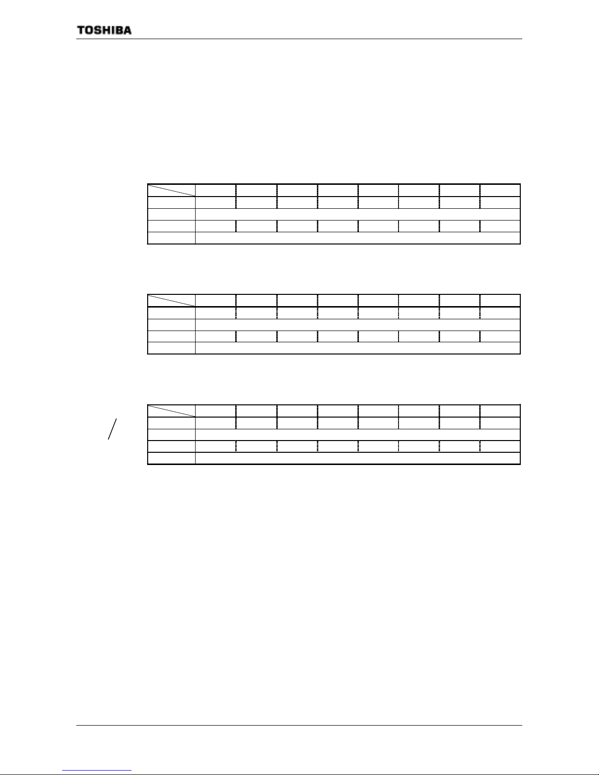
TMP91C824
91C824-80
(2) Memory Address Mask Registers
Figure 3.6.3 shows the Memory Address Mask Registers. Memory address mask registers
MAMR0 to MAMR3 are used to set the size of the CS0 to CS3 areas by specifying a mask for each
bit of the start address set in memory start address registers MAMR0 to MAMR3. The compare
operation used to determine if an address is in the CS0 to CS3 areas is only performed for bus
address bits corresponding to b its set to “0” in these registers. Also, the address bits that can be
masked by MAMR0 to MAMR3 differ between CS 0 to CS3 areas. According ly, the size that can be
each area is different.
Memory add r ess mask r eg ister (for CS0 ar ea)
76543210
bit Symbol V20 V19 V18 V17 V16 V1 5 V14 t o 9 V8
Read/Write R/W
After Reset11111111
Functio n Sets s ize of CS0 ar ea 0: used for ad dr e ss c ompar e
Range of possib le set t ings f or CS0 area size: 256 by t es t o 2 Mbytes
Memory address mask register (CS1)
76543210
bit Symbol V21 V20 V19 V18 V17 V1 6 V15 t o 9 V8
Read/Write R/W
After Reset11111111
Functio n Sets size of CS1 area 0: Used for addr e ss compar e
Range of possib le set t ings f or CS1 area size: 256 by t es t o 4M bytes.
Memory address mask register (CS2, CS3)
76543210
bit Symbol V22 V21 V20 V19 V18 V1 7 V16 V15
Read/Write R/W
After rese t 1 1 1 1 1 1 1 1
Functio n Sets size of CS2 or CS3 ar ea 0: used for ad dr e ss c ompar e
Range of poss ible set t in gs f or CS2 and CS3 area sizes: 3 2 Kbytes to 8 Mbytes.
MAMR0
(00C9H)
MAMR1
(00CBH)
MAMR2
(00CDH)
MAMR3
(00CFH)
Figure 3.6.3 Memory Address mask Registers
Page 84
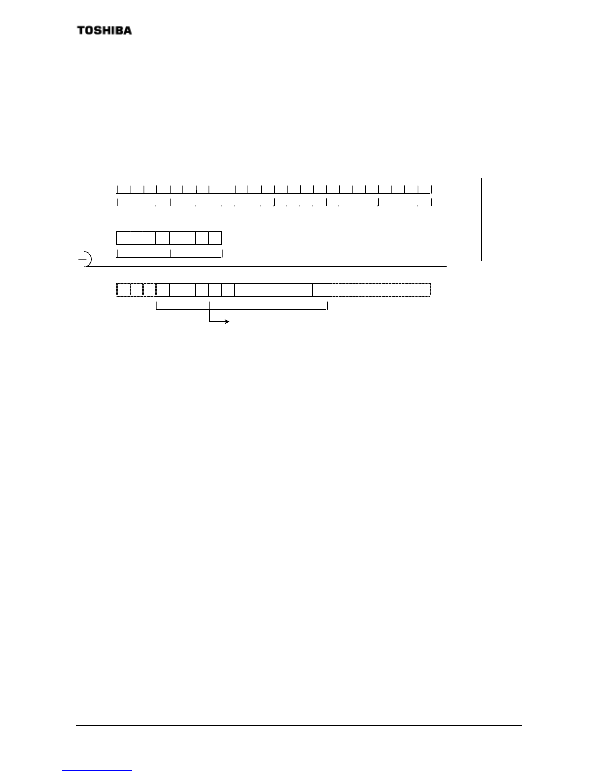
TMP91C824
91C824-81
(3) Setting Memory Start Addresses and Address Areas
Figure 3.6.4 show an example of specifying a 64K-byte address area starting from 010000H
using the CS0 areas.
Set “01H” in memory start addres s regi ster MSA R0<S23 t o S16>(corresp ondi ng to th e upper 8 bit s
of the start address). Next, calculate the difference betw een the st art address an d the anticipated en d
address (01FFFFH). Bits 20 to 8 of the result correspond to the mask value to be set for the CS0 area.
Setting this value in memory address mask register MAMR0<V20 to V8>sets the area size This
example sets “07H” in MAMR0 to specify a 64K-byte area.
000000011111111111111111
01FFFF
S23 S22 S21 S20 S19 S18 S17 S16
00000001
01H
V20 V19 V18 V17 V16 V15 V14 ∼ V9 V8
000000001111111111111111
07H
H
Memory
end
address
Memory
start
address
CSO area
size
(64 Kbytes)
Memory address
mask register
setting
H
MSAR0
MSMR0
Setting of 07H specifies a 64-Kbyte area.
Figure 3.6.4 Example showing how to set the CS0 area
After a reset, MSAR0 to MSAR3 and MAMR0 to MAMR3 are set to “FFH”.B0CS<B0E>,
B1CS<B1E> and B3CS<B3E> are reset to “0”.this disabling the CS0, CS1 and CS3 areas.
However, as B2CS<B2M> to “0” and B2CS<B2E> to “1”, CS2 is enabled from
000FE0H-000FFFH to 003000H-FFFFFFH in TMP91C824. Also, the bus width and number of
waits specified in BEXCS are used for accessing addresses outside the specified CS0 to CS3 area.
(See 3.6.2, Chip Select/Wait Control Registers.)
Page 85
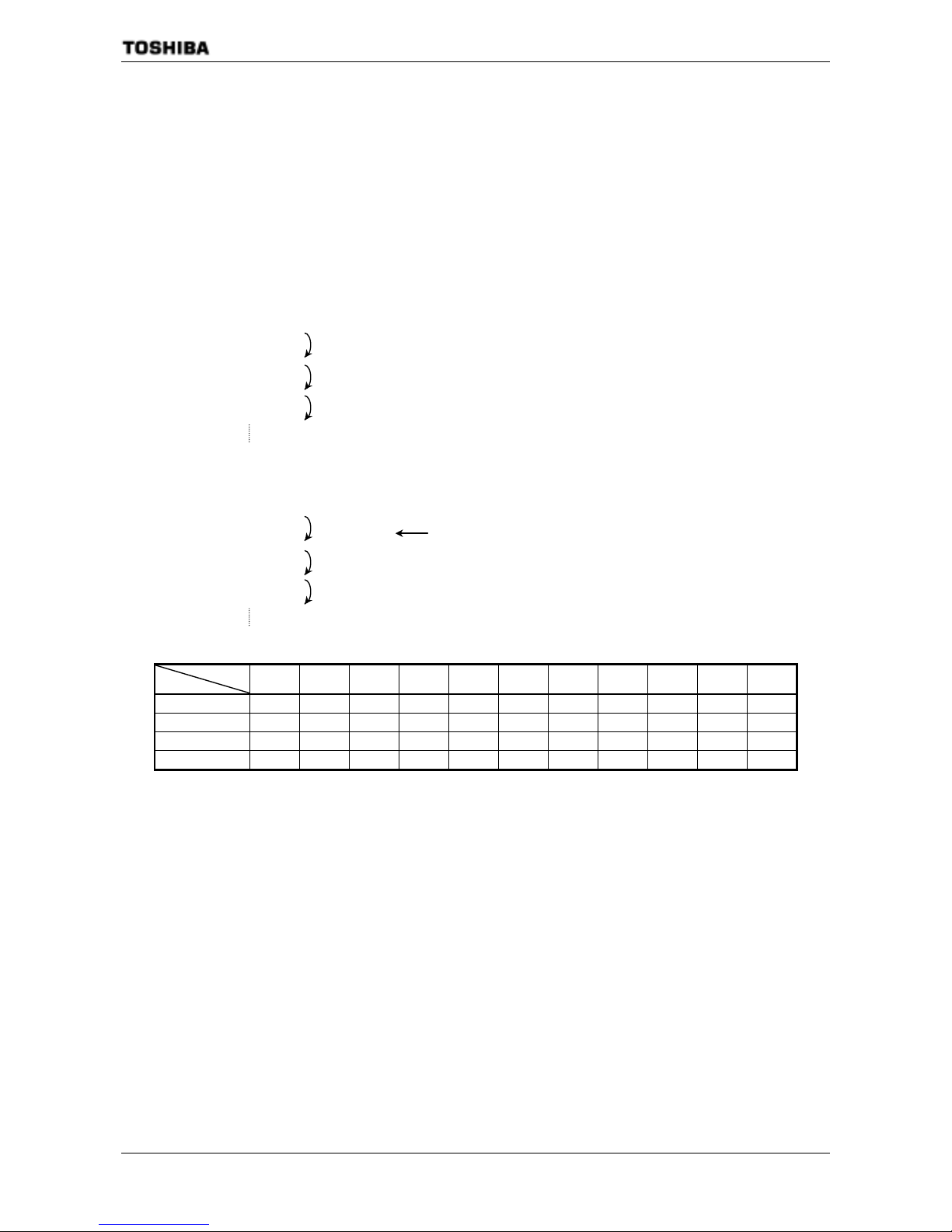
TMP91C824
91C824-82
(4) Address Area Size Specification
Table 3.6.1 shows the relationship between CS area and area size.△ Indicates areas that cannot
be set by memory start address register and address mask register combinations. When setting an
area size using a combination indicated by △ , set the start address mask register in the desired steps
starting from 000000H.
If the CS2 area is set to 16M-bytes or if two or more areas overlap, the smaller CS area number
has the higher priority.
Example: To set the area size for CS0 to 128 Kbytes:
! Valid start addresses
000000H
020000H
040000H
060000H
128K bytes
128K bytes
128K bytes
Any of these addresses may be set as the start address.
" Invalid start addresses
000000H
010000H
030000H
050000H
64K bytes
128K bytes
128K bytes
This is not an integer multiple of the desired area size setting.
Hence, none of these addresses can be set as the start address.
Table 3.6.1 Valid area sizes for each CS area
Size (bytes)
CS area
256 512 32 K 64 K 128 K 256 K 512 K 1 M 2 M 4 M 8 M
CS0
○ ○ ○ ○ △ △ △ △ △
CS1
○ ○
○ △ △ △ △ △ △
CS2
○ ○ △ △ △ △ △ △ △
CS3
○ ○ △ △ △ △ △ △ △
(note):
△
Indicates areas that cannot be set by memory start address register
and address mask register combinations.
3.6.2 Chip Select/Wait Control Registers
Figure 3.6.5 lists the Chip Select/Wait Contro l Registers.
The Master Enable/Disable, Chip Select output waveform, data bus width and number of wait states for
each address area (CS0 to CS3 and others) are set in their respective chip select/wait control registers,
B0CS to B3CS and BEXCS.
Page 86
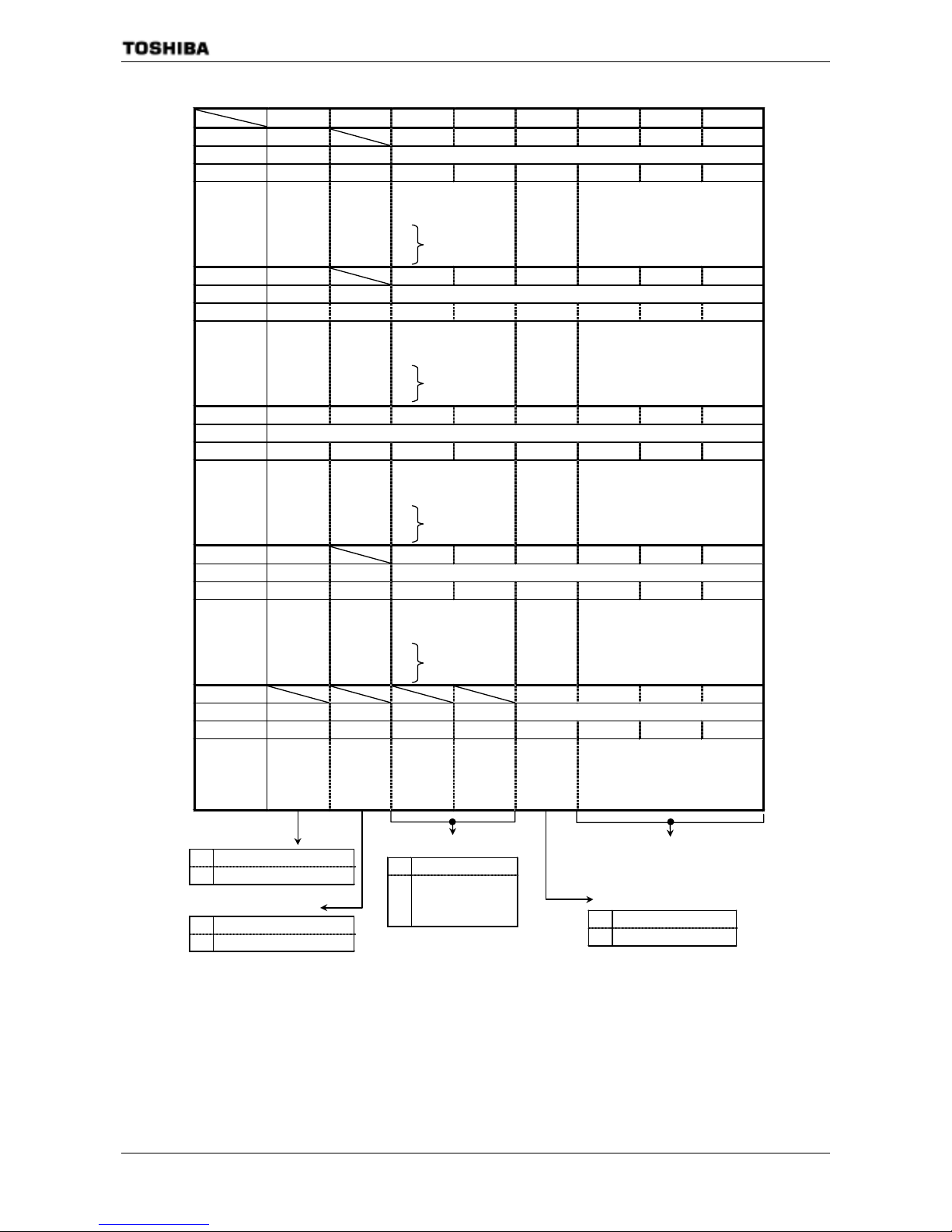
TMP91C824
91C824-83
Chip Select/Wait Control Register
76543210
Bit symbol B0E B0OM1 B0OM0 B0BUS B0W2 B0W1 B0W0
Read/Write W W
After Reset0 000000
Function
0: Disable
1: Enabl e
Chip Select o u tput
waveform sel ection
00: For ROM/SRAM
01:
10: Don ’t care
11:
Data bus
width
0: 16 bits
1: 8 bits
Number of Waits
000: 2 waits 100: reserved
001: 1 wait 101: 3 waits
010: 1 wait + N110: 4 waits
011: 0 waits 111: 8 waits
Bit Symbol B1E B1OM1 B1OM0 B1BUS B1W2 B1W1 B1W0
Read/Write W W
After Reset0 000000
Function
0: Disable
1: Enabl e
Chip Select o u tput
waveform sel ection
00: For ROM/SRAM
01:
10: Don ’t care
11:
Data bus
width
0: 16 bits
1: 8 bits
Number of Waits
000: 2 waits 100: reserved
001: 1 wait 101: 3 waits
010: 1 wait + N110: 4 waits
011: 0 waits 111: 8 waits
Bit Symbol B2E B2M B2OM1 B2OM0 B2BUS B2W2 B2W1 B2W0
Read/Write W
After Reset1000 0000
Functions
0: Disable
1: Enabl e
CS2 area
selection
0: 16-Mbyte
area
1: CS area
Chip Select o u tput
waveform sel ection
00: For ROM/SRAM
01:
10: Don ’t care
11:
Data bus
width
0: 16 bits
1: 8 bits
Number of w aits
000: 2 waits 100: reserved
001: 1 wait 101: 3 waits
010: 1 wait + N110: 4 waits
011: 0 waits 111: 8 waits
Bit Symbol B3E B3OM1 B3OM0 B3BUS B3W2 B3W1 B3W0
Read/Write W W
After Reset0 000000
Functions
0: Disable
1: Enabl e
Chip Select o u tput
waveform sel ection
00: For ROM/SRAM
01:
10: Don ’t care
11:
Data bus
width
0: 16 bits
1: 8 bits
Number of w aits
000: 2 waits 100: reserved
001: 1 wait 101: 3 waits
010: 1 wait + N110: 4 waits
011: 0 waits 111: 8 waits
Bit Symbol BEXBUS BEXW2 BEXW1 BEXW0
Read/Write 0
After Reset 0 0 0 0
Functions
Data bus
width
0: 16 bits
1: 8 bits
Number of Waits
000: 2 waits 100: reserved
001: 1 wait 101: 3 waits
010: 1 wait + N110: 4 waits
011: 0 waits 111: 8 waits
Chip select output waveform
selection
00 For ROM/SRAM
01
1011Don’t care
Master enable bit
0 Enable
1Disable
B0CS
(00C0H)
ReadModifyWrite
instructions
are
prohibited.
B1CS
(00C1H)
ReadModifyWrite
instructions
are
prohibited.
B2CS
(00C2H)
ReadModifyWrite
instructions
are
prohibited.
B3CS
(00C3H)
ReadModifyWrite
instructions
are
prohibited.
BEXCS
(00C7H)
ReadModifyWrite
instructions
are
prohibited.
CS2 area selection
0 1 6-Mbyt e area
1 S pecifi ed ad d ress ar e a
Data bus width selection
0 16-bit data bus
1 8-bit data bus
Number of address area waits
(See 3.6.2, (3) Wait Control.)
Figure 3.6.5 Chip Select/Wait Control Registers
Page 87
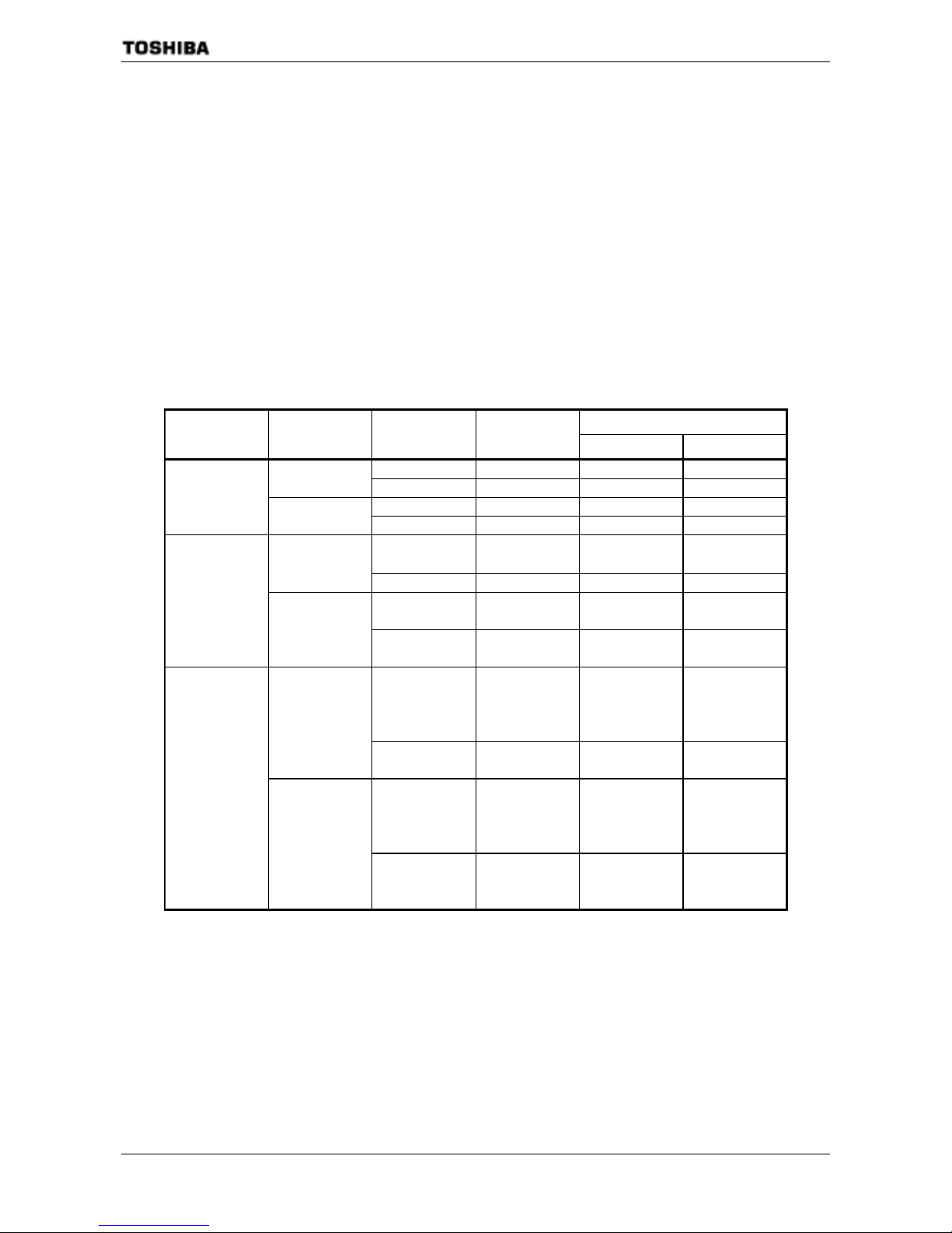
TMP91C824
91C824-84
(1) Master Enable bits
Bit 7 (<B0E>, <B1E>, <B2E> or <B3E>) of a chip select/wait control register is the master bit
which is used to enable or disable settings for the corresponding address area. Writing “1” to this bit
enables the settings. Reset disables (sets to “0”)<B0E>, <B1E> and <B3E>, and enabled (sets to
“1”) <B2E>. This enables area CS2 only.
(2) Data bus width selection
Bit 3 (<B0BUS>, <B1BUS>, <B2BUS>, <B3BUS> or <BEXBUS>) of a chip select/wait control
register specifies the width of the data bus. This bit should be set to “0” when memory is to be
accessed using a 16-bit data bus and to “1” when an 8-bit data bus is to be used.
This process of changing the data bus width according to the address being accessed is known as
“dynamic bus sizing”. For details of this bus operation see Table 3.6.2.
Table 3.6.2 Dynamic bus sizing
CPU Data
Operand Data
Bus Widt h
Operand Start
Address
Memory Data
Bus Widt h
CPU Address
D15 to D8 D7 to D0
8 bits 2n + 0 xxxxx b7 ~ b0 2n + 0
(Even number)
16 bits 2n + 0 xxxxx b7 ~ b0
8 bits 2n + 1 xxxxx b7 ~ b0
8 bits
2n + 1
(Odd number)
16 bits 2n + 1 b7 ~ b0 xxxxx
2n + 0 xxxxx b7 ~ b0 8 bits
2n + 1 xxxxx b15 ~ b8
2n + 0
(Even number)
16 bits 2n + 0 b15 ~ b8 b7 ~ b0
2n + 1 xxxxx b7 ~ b0 8 bits
2n + 2 xxxxx b15 ~ b8
2n + 1 b7 ~ b0 xxxxx
16 bits
2n + 1
(Odd number)
16 bits
2n + 2 xxxxx b15 ~ b8
2n + 0 xxxxx b7 ~ b0
2n + 1 xxxxx b15 ~ b8
2n + 2 xxxxx b23 ~ b16
8 bits
2n + 3 xxxxx b31 ~ b24
2n + 0 b15 ~ b8 b7 − b0
2n + 0
(Even number)
16 bits
2n + 2 b31 ~ b24 b23 − b16
2n + 1 xxxxx b7 ~ b0
2n + 2 xxxxx b15 ~ b8
2n + 3 xxxxx b23 ~ b16
8 bits
2n + 4 xxxxx b31 ~ b24
2n + 1 b7 ~ b0 xxxxx
2n + 2 b23 ~ b16 b15 ~ b8
32 bits
2n + 1
(Odd number)
16 bits
2n + 4 xxxxx b31 ~ b24
(note): “xxxxx” indicates that the input data from these bits are ignored during a read. During a write, indicates
that the bus for these bits goes too high-impedance; also, that the write strobe signal for the bus remains inactive.
Page 88
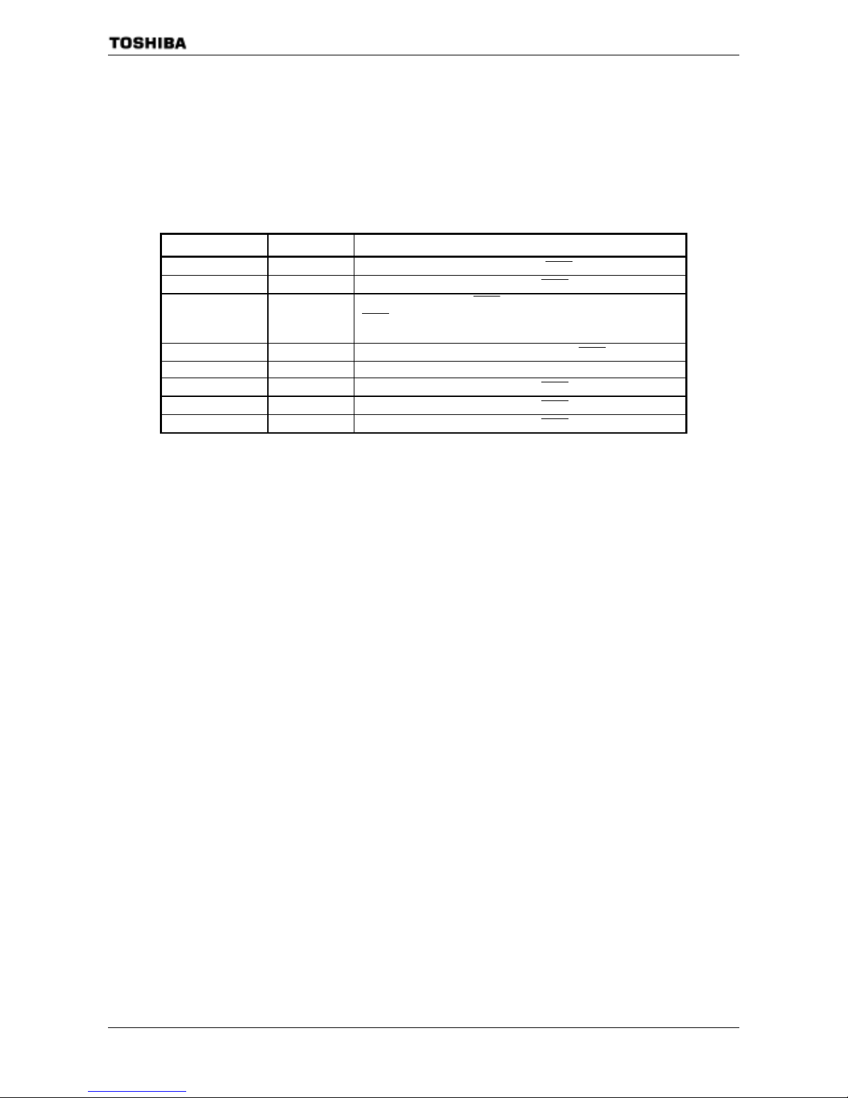
TMP91C824
91C824-85
(3) Wait control
Bits 0 to 2 (<B0W0 to B0W2>, <B1W0 to B1W2>, <B2W0 to B2W2>, <B3W0 to B3W2>,
<BEXW0 to BEXW2>) of a chip select/wait control register specify the number of waits that are to
be inserted when the corresponding memory area is accessed.
The following types of wait operation can be specified using these bits. Bit settings other than those
listed in the table should not be made.
Table 3.6.3 Wait operation settings
<BxW2 ~ BxW0> No. of Waits Wait Operation
000 2WAIT
Inserts a wait of 2 states, irrespective of the
WAIT
pin state.
001 1WAIT
Inserts a wait of 1 state, irrespective of the
WAIT
pin state.
010 1WAIT + N S amples t he state of t he WAIT pin after in serting a wait of one s tate. If th e
WAIT
pin is Low, the waits continue and the bus cycle is extended until the
pin goes high.
011 0WAIT
Ends the bus cycle without a wait , regardless of the
WAIT
pin state.
100 Reserved Invalid setting
101 3WAIT
Inserts a wait of 3 state, irrespective of the
WAIT
pin state.
110 4WAIT
Inserts a wait of 4 state, irrespective of the
WAIT
pin state.
111 8WAIT
Inserts a wait of 8 state, irrespective of the
WAIT
pin state.
A Reset sets these bits to “000” (2 waits).
(4) Bus width and wait control for an area other than CS0 to CS3
The chip select/wait control register BEXCS controls the bus width and number of waits when
memory locations which are not in one of the four user-specified address areas (CS0 to CS3) are
accessed. The BEXCS register settings are always enabled for areas other than CS0 to CS3.
(5) Selecting 16-Mbyte area/specified address area
Setting B2CS<B2M> (bit 6 of the chip select/wait control register for CS2) to “0” designates the
16-Mbyte area 000FE0H-000FFFH, 003000H-FFFFFFH as the CS2 area. Setting B2CS<B2M> to
“1” designates the address area specified by the start addres s regist er MSAR2 and the address mask
register MAMR2 as CS2 (i.e. if B2CS<B2M> = 1, CS2 is specified in th e same manner as CS0, C S1
and CS3 are).
A Reset clears this bit to “0”, specifying CS2 as a 16-M bytes address area.
Page 89

TMP91C824
91C824-86
(6) Procedure for setting chip select/wait control
When using the chip select/wait control function, set the registers in the following order:
! Set the Memory Start Address Registers MSAR0 to MSAR3.
Set the start addresses for CS0 to CS3.
" Set the Memory Address Mask Registers MAMR0 to MAMR3.
Set the sizes of CS0 to CS3.
# Set the chip select/wait control registers B0CS to B 3CS.
Set the Chip Select output waveform, data bus width, number of waits and Master
Enable/Disable status for /CS0 to /CS3.
The CS0 to S3 pins can also function as pins P60 to P63. To output a Chip Select signal
using one of thes e pins, set the corresponding bit in the Port 6 F u nction Register P6FC to “1”.
If a CS0 “to S3 address is specified which is actually an internal I/O and RAM area address,
the CPU accesses the internal address area and no Chip Select signal is output on any of the
/CS0 to /CS3 pins.
Setting example:
In this example CS0 is set to be the 64-Kbyte area 010000H to 01FFFFH. The bus width is set to 16 bits
and the number of waits is set to 0.
MSAR0 = 01H............... Start address: 010000H
MAMR0 = 07H .............Address area: 64 Kbytes
B0CS = 83H...................ROM/SRAM, 16-bit data bus, zero waits, CS0 area settings enabled
Page 90
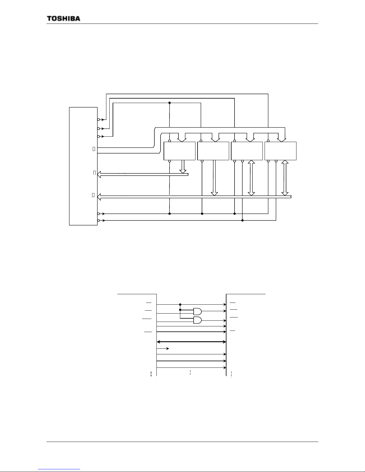
TMP91C824
91C824-87
3.6.3 Connecting external memory
Figure 3.6.6 shows an example of how to connect external memory to the TMP91C824.
In this example the ROM is connected using a 16-bit bus. The RAM and I/O are connected using an 8-bit
bus.
Address bus
___
CS
8-bit
RAM
___
OE
___
WE
TMP91C824
〜
〜
___
CS
Upper byte
ROM
___
OE
___
CS
Lower byte
ROM
___
OE
___
CS
8-bit
I/O
___
OE
___
WE
____
CS0
____
CS1
____
CS2
A0
A23
D8
D15
D0
D7
___
RD
___
WR
〜
Figure 3.6.6 Example of external memory connection
(ROM uses 16-bit bus; RAM and I/O use 8-bit bus.)
A Reset clears all bits of the Port 6 Control Register P6CR and the Port 6 Function Register P6FC to
“0” and disables output of the CS signal. To output the CS signal, the appropriate bit must be set to “1”.
Figure 3.6.7 Example of external memory connection (RAM and I/O use 16-bit bus)
OE
LDS
UDS
R/W
CE
I/O [16:1]
A0 A1 A
2
RD
WR
HWR
R/W
CS0
D [15:0]
A0
A1
A2
A3
TMP91C824F 16-bit SRAM
Page 91
TMP91C824
91C824-88
3.7 8-bit Timers (TMRA)
The TMP91C824 features 4 channel(TMRA0 to TMRA3) built-in 8-bit timers.
These timers are paired into 2 modu les: TMRA 01 and TMRA 23. Each module cons ists of 2 channels and can
operate in any of the following 4 operating modes.
• 8-Bit Interval Timer Mode
• 16-Bit Interval Timer Mode
• 8-Bit Programmable Square Wave Pulse Generation Output Mode (PPG: variable duty cycle with
variable period)
• 8-Bit Pulse Width Modulation Output Mode (PWM – variable duty cycle with constant period)
Figure 3.7.1 to Figure 3.7.2 Show block diagrams for TMRA01 and TMRA23.
Each channel consists of an 8-bit up counter, an 8-bit comparator and an 8-bit timer register. In addition, a
timer flip-flop and a prescaler are provided for each pair of channels.
The operation mode and timer flip-flop condition are controlled by 5bytes registers.
We call control registers SFRs: Special Function Registers.
Each of the two modules (TMRA 01 and TMRA 23) can be operated indepen dently . All module s operate i n th e
same manner; hence only the operation of TMRA01 is explained here.
The contents of this chapter are as follows.
3.7.1 Block diagrams
3.7.2 Operation of each circuit
3.7.3 SFRs
3.7.4 Operation in each mode
(1) 8-Bit Timer Mode
(2) 16-Bit Timer Mode
(3) 8-Bit PPG (programmable pulse generation) Output Mode
(4) 8-Bit PWM (pulse width modulation) Output Mode
(5) Mode settings
Table 3.7.1 Registers and pins for each module
Module
TMRA01 TMRA23
Input pin for external
clock
TA0IN
(shared with PB0)
None
External
pin
Output pin for timer
flip-flop
TA1OUT
(shared with PB1)
TA3OUT
(shared with PB2)
Timer run register TA01RUN (0100H) TA23RUN (0108H)
Timer register
TA0REG (0102H)
TA1REG (0103H)
TA2REG (010AH)
TA3REG (010BH)
Timer mode register TA01MOD (0104H) TA23MOD (010CH)
SFR
(address)
Timer flip-flop control
register
TA1FFCR (0105H) TA3FFCR (010DH)
Page 92
TMP91C824
91C824-89
3.7.1 Block diagrams
Run/Clear
Prescaler
clock: φT0
TA0TRG
External input
clock: TA0IN
TA01MOD
<PWM01,
PWM0100>
Selector
8-Bit Up-Counter
(UC1)
8-Bit comparator
(CP1)
8-bit up counte r
(UC0)
8-Bit Timer
Register TA1REG
8-Bit up counter
(CP0)
Match
detect
Register bu ffe r 0
8-Bit timer register
TA0REG
TA01RUN
<TA0RDE>
TA01RUN<TA0RUN>
φ
T1
φ
T4
φ
T16
2
n
−
1
Over flow
TMRA0
Interrupt ou tp ut :
INTTA0
TA01MOD
<TA01M1,
TA01M 0>
TMRA0
Match outpu t:
TA0TRG
Selector
φ
T1
φ
T16
φ
T256
Internal bus
TA01MOD
<TA0CLK1, TA0CLK10>
TA01MOD
<TA1CLK1, TA1CLK 0>
Match
detect
TMRA1
Interrupt ou tp ut :
INTTA1
TA01RUN<TA1RUN>
Timer
Flip-Flop
TA1FF
TA1FFCR
Timer flip-flop
output:
TA1OUT
512 256 128
64 3216 8 4 2
φ
T1 φT4 φT16
φ
T256
Prescaler
TA01RUN
<TA01PRUN>
Internal bus
Figure 3.7.1 TMRA01 block diagram
Page 93
TMP91C824
91C824-90
Run/clea
Prescaler
clock: φT0
TA2TR
TA23MOD
<PWM21,
PWM20>
Selector
8-bit Comparator
(CP3)
8-bit Up -Counter
(UC2)
8-bit timer
Register TA3REG
8-bit Comparator
(CP2)
Match
detect
Register Buf fer 2
TA23RUN
<TA2RDE>
TA23RUN<TA2RUN>
φ
T1
φ
T4
φ
T16
2
n
−
1
Over flow
TMRA2
Interrupt ou tp ut :
INTTA2
TA23MOD
<TA23M1,
TA23M10 >
TMRA2
Match outpu t:
TA2TRG
Selector
φ
T1
φ
T16
φ
T256
Internal bus
TA23MOD
<TA3CLK1:0>
Match
detect
TMRA3
Interrup out pt u:
INTTA3
TA23RUN<TA3RUN>
Timer
flip-flop
TA3FF
TA3FFCR
Timer flip-flop
output:
TA3OUT
512 256
128
64 32 16 8 4 2
φ
T1 φT4 φT16
φ
T256
Prescaler
TA23RUN
<TA23PRUN>
Internal bus
8-bit Up -Counter
(UC3)
8-bit Timer
Register TA2REG
TA23MOD
<TA2CLK1, TA2CLK 0>
Figure 3.7.2 TMRA23 block diagram
Page 94
TMP91C824
91C824-91
3.7.2 Operation of each circuit
(1) Prescalers
A 9-bit prescaler generates the input clock to TMRA01.
The “φT0” as the inpu t clock to prescaler is a cl ock divided by 4 wh ich selected using the Prescaler
Clock Selection Register SYSCR0<PRCK1,PRCK0>.
The prescaler’s operation can be controlled using TA01RUN<TA0PRUN> in the timer control
register. Setting <TA0PRUN> to “1” starts the count; setting <TA0PRUN> to “0” clears the
prescaler to zero and stops operation. Table 3.7 (2) shows the various prescaler output clock
resolutions.
Table 3.7.2 Prescaler output clock resolution
@fc = 16 MHz, fs = 32.768 kHz
Prescaler Output Clock Resolution
System Clock
Selection
<SYSCK>
Prescaler Clock
Selection
<PRCK1,PRCK0>
Gear Value
<GEAR2~GEAR0>
φT1 φT4 φT16 φT256
1 (fs) XXX fs/23 (244 µs) fs/25 (977 µs) fs/27 (3.9 µs) fs/211 (62.5 µs)
000 (fc) fc/23 (0.5 µs) fc/25 (2.0 µs) fc/27 (8.0 µs) fc/211 (128 µs)
001 (fc/2)
fc/2
4
(1.0 µs) fc/26 (4.0 µs) fc/28 (16 µs) fc/212 (256 µs)
010 (fc/4)
fc/2
5
(2.0 µs) fc/27 (8.0 µs) fc/29 (32 µs) fc/213 (512 µs)
011 (fc/8)
fc/2
6
(4.0 µs) fc/28 (16 µs) fc/210 (64 µs) fc/214 (1024 µs)
00
(f
FPH
)
100 (fc
/16
)
fc/2
7
(8.0 µs) fc/29 (32 µs) fc/211 (128 µs) fc/215 (2048 µs)
0 (fc)
10
(fc
/16 CLOCK)
XXX fc/2
7
(8.0 µs) fc/29 (32 µs) fc/211 (128 µs) fc/215 (2048 µs)
xxx: Don't care
(2) Up-counters (UC0 and UC1)
These are 8-bit binary counters which count up the input clock pulses for the clock specified by
TA01MOD.
The input clock for UC0 is selectable and can be either the external clock input via the TA0IN pin or
one of the three internal clocks φT1, φT4 or φT16. The clock setting is specified by the value set
in TA01MOD<TA01CLK1,TA01CLK0>.
The input clock for UC1 depends on the operation mode. In 16-Bit Timer Mode, the overflow
output from UC0 is used as the input clock. In any mode other than 16-Bit Timer Mode, the input
clock is selectable and can either be one of the internal clocks φT1, φT16 or φT2 56, or the
comparato r output (the match detect ion signal) fr om TMRA0.
For each interval timer the timer operation control register bits TA01RUN<TA0RUN> and
TA01RUN<TA1RUN> can be used to stop and clear the up-counters and to control their count. A
Reset clears both up-counters, stopping the timers.
Page 95
TMP91C824
91C824-92
(3) Timer registers (TA0REG and TA1REG)
These are 8-bit registers which can be used to set a time interval. When the value set in the timer
register TA0REG or TA1REG matches the value in the corresponding up -counter, the Comparator
Match Detect signal goes Active. If the value set in the timer register is 00H, the signal goes Active
when the up-counter overflows.
The TA0REG are double buffer structure, each of which makes a pair with register buffer.
The setting of the bit TA01RUN<TA0RDE> determines whether TA0REG’s double buffer
structure is enabled or disabled. It is disabled if < TA0RDE> = “0” and enabled if <TA0RDE> = “1”.
When the double buffer is enabled, data is transferred from the register buffer to the timer register
when a 2
n
−1 overflow occurs in PWM Mode, or at the start of the PPG cycle in PPG Mode. Hence
the double buffer cannot be used in Timer Mode.
A Reset initializes <TA0RDE> to “0”, disabling the double buffer. To use the double buffer, write
data to the timer register, set <TA0RDE> to “1”, and write the following data to the register buffer.
Figure 3.7.3 show the configuration of TA0REG.
Selector
Y
S
A
B
Write
Shift trigger
Write to TA0REG
2
n
-1 overf low of PW M
TA01RUN<TA0RDE>
Up-counter
Comparator (CP0)
Timer Re gisters 0 (TA0REG)
Register Buffers 0
Internal bus
Matching detection in PPG cycle
Figure 3.7.3 Configuration of TA0REG
(note): The same memory address is allocated to the timer register and the register buffer. When <TA0RDE>
= 0, the same value is written to the register buffer and the timer register; when <TA0RDE> = 1, only
the register buffer is written to.
The address of each timer register is as follows.
TA0REG: 000102H TA1REG: 000103H
TA2REG: 00010AH TA3REG: 00010BH
All these registers are write only and cannot be read.
Page 96

TMP91C824
91C824-93
(4) Comparator (CP0)
The comparator compares the value in an up counter w ith the value s et in a tim er reg is ter. If th ey
match, the up counter is cleared to zero and an interrupt signal (INTTA0 or INTTA1) is generated.
If timer flip-flop inversion is enabled, the timer flip-flop is in verted at the same time.
(5) Timer flip-flop (TA1FF)
The timer flip-flop (TA1FF) is a flip-flop inverted by the match detects signal (8-bit comparator
output) of each interval timer.
Whether inversion is enabled or disabled is determined by the setting of the bit
TA1FFCR<TAFF1IE> in the T imer Flip-Flop Control Register.
A Reset clears the value of TA1FF1 to “0”.
Writing “01” or ”10” to TA1FFCR <TAFF1C[1:0]> s ets TA1FF t o 0 or 1. Writing “00” to th ese bits
inverts the va lue of TA1FF (this is known as software inversio n).
The TA1FF signal is ou tput via t he TA1OUT pin (concurrent w ith PB1). Wh en th is pin is used as
the timer output, the timer flip-flop should b e set beforehand using the Port B Function Register
PBCR,PBFC.
Page 97
TMP91C824
91C824-94
3.7.3 SFRs
TMRA01 Run Register
76543210
Bit symbol TA0RDE I2TA01
TA01PRUN
TA1RUN TA0RUN
Read/Write R/W R/W
After Reset0 0000
Function
Double
buffer
0: Disable
1: Enable
IDLE2
0: Stop
1: Operate
Timer Run/Stop control
0: Stop & Clear
1: Run (count up)
TA01RUN
(0100H)
Timer Run/Stop control
0 Stop & Clear
1 Run (count up)
TA0REG double buffer control
0Disable
1 Enable
I2TA01 : Operation in IDLE2 Mode
TA01PRUN : Run prescaler
TA1RUN : Run Timer 1
TA0RUN : Run Timer 0
(note): The values of bits 4,5,6 of TA01RUN are undefined when read.
TMRA23 Run Register
76543210
Bit symbol TA2RDE I2TA23
TA23PRUN
TA3RUN TA2RUN
Read/Write R/W R/W
After Reset0 0000
Function
Double
buffer
0: Disable
1: Enable
IDLE2
0: Stop
1: Operate
Timer Run/Stop control
0: Stop & Clear
1: Run (count up)
TA23RUN
(0108H)
Ti m er Run/Stop control
0 Stop & Clear
1 R un (count up)
TA2REG double buffer control
0Disable
1 Enable
I2TA23 : Operation in IDLE2 Mode
TA23PRUN : Run prescaler
TA3RUN : Run Timer 3
TA2RUN : Run Timer 2
(note): The values of bits 4,5,6 of TA23RUN are undefined when read.
Figure 3.7.4 TMRA Registers
Page 98
TMP91C824
91C824-95
TMRA01 Mode Register
76543210
Bit symbol TA01M1 TA01M0 PWM01 PWM00 TA1CLK1 TA1CLK0 TA0CLK1 TA0CLK0
Read/Write R/W
After Reset00000000
Function
Operation mode
00: 8-Bit Timer Mode
01: 16-Bit Timer Mode
10: 8-Bit PPG Mode
11: 8- Bit P W M Mo de
PWM cycle
00: reserved
01: 2
6
-1
10: 2
7
-1
11: 2
8
-1
Source clock for TMRA1
00: TA0TRG
01: φT1
10: φT16
11: φT256
Source clock f or TMRA0
00: TA0IN pin
01: φT1
10: φT4
11: φT16
00 TA0IN (external input)
01φT1 (prescaler)
10φT4 (prescaler)
11φT16 (prescaler)
TA01MOD
<TA01M1∼TA01M0>≠01
TA01MOD
<TA01M1∼TA01M 0>=01
00
Comparator
output from TMRA0
01φT1
10φT16
11
φT
256
Overflow output from
TMRA0
(16-Bit Timer Mode)
00 reserved
01 (26-1) × clock source
10 (27-1) × clock source
11 (28-1) × clock source
00 Two 8-bit timer s
01 16- b it timer
10 8- bit PPG
11 8- bit PWM ( TMRA0) + 8- bit t imer ( T M RA1)
PWM cycle selection
TA01MOD
(0104H)
TMRA0 source clock selection
TMRA1 source clock selection
TMRA01 operation mode selection
Figure 3.7.5 TMRA registers
Page 99
TMP91C824
91C824-96
TMRA23 Mode Register
76543210
Bit Symbol TA23M1 TA23M0 PWM21 PWM20 TA3CLK1 TA 3CLK 0 T A 2CLK 1 TA 2CLK 0
Read/Write R/W
After Reset00000000
Function
Operation mode
00: 8-Bit Timer Mode
01: 16-Bit Timer Mode
10: 8-Bit PPG Mode
11: 8-Bit PWM Mode
PWM cycle
00: reserved
01: 2
6
-1
10: 2
7
-1
11: 2
8
-1
TMRA3 clock for TMRA3
00: TA2TRG
01:
φ
T1
10:
φ
T16
11:
φ
T256
TMRA2 clock for TMRA2
00: reserved
01:
φ
T1
10:
φ
T4
11:
φ
T16
00 Do not set
01φT1 (prescaler)
10φT4 (prescaler)
11φT16 (prescaler)
TA23MOD
<TA23M1∼TA23M0>≠01
TA23MOD
<TA23M1∼TA23M0>=01
00 Comparator output
from TMRA2
01
φ
T1
10
φ
T16
11
φ
T256
Overflow output from
TMRA2
(16-Bit Timer Mode)
00 reserved
01 (26-1) × clock source
10 (27-1) × clock source
11 (28-1) × clock source
00 Two 8-bit timers
01 16-bit timer
10 8-bit PPG
11 8-bit PWM (TMRA2) + 8-bit timer (TMRA3)
PWM cycle selection
TA23MOD
(010CH)
TMRA2 source clock selection
TMRA3 source clock selection
TMRA23 operation mode selection
Figure 3.7.6 TMRA registers
Page 100
TMP91C824
91C824-97
TMRA1 Fli p-Flop Cont rol Register
7 6 5 4 3 2 1 0
Bit symbol TAFF1C1 TAFF1C0 TAFF1IE TAFF1IS
Read/Write R/W R/W
After Reset 1 1 0 0
Function
00: Invert TA1FF
01: Set TA1FF
10: Clear TA1FF
11: Don’t care
TA1FF
Control for
inversion
0: Disable
1: Enable
TA1FF
Inversion
select
0: TMRA0
1: TMRA1
0 Inversion by TMRA0
1 Inversion by TMRA1
0 Disabled
1 Enabled
00 In ver ts th e value of TA1FF
01 Sets TA1FF to “1”
10 Clears TA1FF to “0”
11 Don’t care
Control of TA1FF
TA1FFCR
(0105H)
Inverse signal for Timer Flop-Flop 1 (TA1FF)
(Don’t care except in 8-B it Timer Mode)
Inversi on of TA1FF
Read-Modify
-Write
instructions
are
prohibited.
Figure 3.7.7 TMRA registers
 Loading...