

Page 1

8 Bit Microcontroller
TLCS-870/C Series
TMP86CH22UG
Page 2

TMP86CH22UG
The information contained herein is subject to change without notice. 021023 _ D
TOSHIBA is continually working to improve the quality and reliability of its products. Nevertheless,
semiconductor devices in general can malfunction or fail due to their inherent electrical sensitivity and
vulnerability to physical stress.
It is the responsibility of the buyer, when utilizing TOSHIBA products, to comply with the standards
of safety in making a safe design for the entire system, and to avoid situations in which a malfunction
or failure of such TOSHIBA products could cause loss of human life, bodily injury or damage to
property.
In developing your designs, please ensure that TOSHIBA products are used within specified operating
ranges as set forth in the most recent TOSHIBA products specifications.
Also, please keep in mind the precautions and conditions set forth in the “Handling Guide for
Semiconductor Devices,” or “TOSHIBA Semiconductor Reliability Handbook” etc. 021023_A
The Toshiba products listed in this document are intended for usage in general electronics applications
(computer, personal equipment, office equipment, measuring equipment, industrial robotics, domestic
appliances, etc.).
These Toshiba products are neither intended nor warranted for usage in equipment that requires
extraordinarily high quality and/or reliability or a malfunction or failure of which may cause loss of
human life or bodily injury (“Unintended Usage”). Unintended Usage include atomic energy control
instruments, airplane or spaceship instruments, transportation instruments, traffic signal instruments,
combustion control instruments, medical instruments, all types of safety devices, etc. Unintended
Usage of Toshiba products listed in this document shall be made at the customer's own risk. 021023_B
The products described in this document shall not be used or embedded to any downstream products
of which manufacture, use and/or sale are prohibited under any applicable laws and regulations.
060106_Q
The information contained herein is presented only as a guide for the applications of our products. No
responsibility is assumed by TOSHIBA for any infringements of patents or other rights of the third
parties which may result from its use. No license is granted by implication or otherwise under any
patent or patent rights of TOSHIBA or others. 021023_C
The products described in this document may include products subject to the foreign exchange and
foreign trade laws. 021023_F
For a discussion of how the reliability of microcontrollers can be predicted, please refer to Section 1.3
of the chapter entitled Quality and Reliability Assurance/Handling Precautions. 030619_S
© 2006 TOSHIBA CORPORATION
All Rights Reserved
Page 2
Page 3

Revision History
Date Revision
2005/12/8 1 First Release
2006/9/8 2 Contents Revised
2008/8/29
3 Contents Revised
Page 4
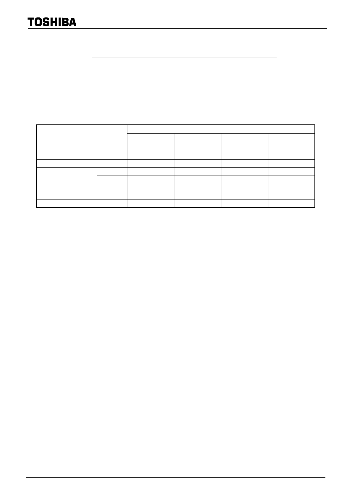
Caution in Setting the UART Noise Rejection Time
When UART is used, settings of RXDNC are limited depending on the transfer clock specified by BRG. The com-
bination "O" is available but please do not select the combination "–".
The transfer clock generated by timer/counter interrupt is calculated by the following equation :
Transfer clock [Hz] = Timer/counter source clock [Hz] ÷ TTREG set value
RXDNC setting
BRG setting
000 fc/13 O O O –
110
(When the transfer clock gen-
erated by timer/counter inter-
rupt is the same as the right
side column)
The setting except the aboveOOOO
Transfer
clock [Hz]
fc/8 O – – –
fc/16 O O – –
fc/32OOO–
00
(No noise rejection)
(Reject pulses shorter
than 31/fc[s] as noise)
01
(Reject pulses shorter
than 63/fc[s] as noise)
10
(Reject pulses shorter
11
than 127/fc[s] as
noise)
Page 5

Page 6

Table of Contents
TMP86CH22UG
1.1 Features . . . . . . . . . . . . . . . . . . . . . . . . . . . . . . . . . . . . . . . . . . . . . . . . . . . . . . . . . 1
1.2 Pin Assignment . . . . . . . . . . . . . . . . . . . . . . . . . . . . . . . . . . . . . . . . . . . . . . . . . . . . 3
1.3 Block Diagram . . . . . . . . . . . . . . . . . . . . . . . . . . . . . . . . . . . . . . . . . . . . . . . . . . . . . 4
1.4 Pin Names and Functions . . . . . . . . . . . . . . . . . . . . . . . . . . . . . . . . . . . . . . . . . . . . 5
2. Operational Description
2.1 CPU Core Functions . . . . . . . . . . . . . . . . . . . . . . . . . . . . . . . . . . . . . . . . . . . . . . . . 9
2.1.1 Memory Address Map............................................................................................................................... 9
2.1.2 Program Memory (MaskROM).................................................................................................................. 9
2.1.3 Data Memory (RAM)............................................................................................................................... 10
2.2 System Clock Controller . . . . . . . . . . . . . . . . . . . . . . . . . . . . . . . . . . . . . . . . . . . . 10
2.2.1 Clock Generator...................................................................................................................................... 10
2.2.2 Timing Generator.................................................................................................................................... 12
2.2.2.1 Configuration of timing generator
2.2.2.2 Machine cycle
2.2.3 Operation Mode Control Circuit .............................................................................................................. 13
2.2.3.1 Single-clock mode
2.2.3.2 Dual-clock mode
2.2.3.3 STOP mode
2.2.4 Operating Mode Control ......................................................................................................................... 18
2.2.4.1 STOP mode
2.2.4.2 IDLE1/2 mode and SLEEP1/2 mode
2.2.4.3 IDLE0 and SLEEP0 modes (IDLE0, SLEEP0)
2.2.4.4 SLOW mode
2.3 Reset Circuit . . . . . . . . . . . . . . . . . . . . . . . . . . . . . . . . . . . . . . . . . . . . . . . . . . . . . 31
2.3.1 External Reset Input ............................................................................................................................... 31
2.3.2 Address trap reset .................................................................................................................................. 32
2.3.3 Watchdog timer reset.............................................................................................................................. 32
2.3.4 System clock reset.................................................................................................................................. 32
3. Interrupt Control Circuit
3.1 Interrupt latches (IL19 to IL2) . . . . . . . . . . . . . . . . . . . . . . . . . . . . . . . . . . . . . . . . 35
3.2 Interrupt enable register (EIR) . . . . . . . . . . . . . . . . . . . . . . . . . . . . . . . . . . . . . . . . 36
3.2.1 Interrupt master enable flag (IMF) .......................................................................................................... 36
3.2.2 Individual interrupt enable flags (EF19 to EF4) ...................................................................................... 37
Note 3: . . . . . . . . . . . . . . . . . . . . . . . . . . . . . . . . . . . . . . . . . . . . . . . . . . . . . . . . . . . . . 38
3.3 Interrupt Sequence . . . . . . . . . . . . . . . . . . . . . . . . . . . . . . . . . . . . . . . . . . . . . . . . 39
3.3.1 Interrupt acceptance processing is packaged as follows........................................................................ 39
3.3.2 Saving/restoring general-purpose registers ............................................................................................ 40
3.3.2.1 Using PUSH and POP instructions
3.3.2.2 Using data transfer instructions
3.3.3 Interrupt return ........................................................................................................................................ 41
3.4 Software Interrupt (INTSW) . . . . . . . . . . . . . . . . . . . . . . . . . . . . . . . . . . . . . . . . . . 42
3.4.1 Address error detection .......................................................................................................................... 42
3.4.2 Debugging .............................................................................................................................................. 42
i
Page 7

3.5 Undefined Instruction Interrupt (INTUNDEF). . . . . . . . . . . . . . . . . . . . . . . . . . . . . 42
3.6 Address Trap Interrupt (INTATRAP) . . . . . . . . . . . . . . . . . . . . . . . . . . . . . . . . . . . 42
3.7 External Interrupts . . . . . . . . . . . . . . . . . . . . . . . . . . . . . . . . . . . . . . . . . . . . . . . . . 43
4. Special Function Register (SFR)
4.1 SFR . . . . . . . . . . . . . . . . . . . . . . . . . . . . . . . . . . . . . . . . . . . . . . . . . . . . . . . . . . . . 45
4.2 DBR . . . . . . . . . . . . . . . . . . . . . . . . . . . . . . . . . . . . . . . . . . . . . . . . . . . . . . . . . . . . 47
5. I/O Ports
5.1 Port P1 (P17 to P10) . . . . . . . . . . . . . . . . . . . . . . . . . . . . . . . . . . . . . . . . . . . . . . . 50
5.2 Port P2 (P22 to P20) . . . . . . . . . . . . . . . . . . . . . . . . . . . . . . . . . . . . . . . . . . . . . . . 53
5.3 Port P3 (P37, P34 to P33) . . . . . . . . . . . . . . . . . . . . . . . . . . . . . . . . . . . . . . . . . . . 54
5.4 Port P5 (P57 to P50) . . . . . . . . . . . . . . . . . . . . . . . . . . . . . . . . . . . . . . . . . . . . . . . 56
5.5 Port P6 (P64 to P61) . . . . . . . . . . . . . . . . . . . . . . . . . . . . . . . . . . . . . . . . . . . . . . . 58
5.6 Port P7 (P76 to P70) . . . . . . . . . . . . . . . . . . . . . . . . . . . . . . . . . . . . . . . . . . . . . . . 60
6. Watchdog Timer (WDT)
6.1 Watchdog Timer Configuration . . . . . . . . . . . . . . . . . . . . . . . . . . . . . . . . . . . . . . . 63
6.2 Watchdog Timer Control . . . . . . . . . . . . . . . . . . . . . . . . . . . . . . . . . . . . . . . . . . . . 64
6.2.1 Malfunction Detection Methods Using the Watchdog Timer ................................................................... 64
6.2.2 Watchdog Timer Enable ......................................................................................................................... 65
6.2.3 Watchdog Timer Disable ........................................................................................................................ 66
6.2.4 Watchdog Timer Interrupt (INTWDT)...................................................................................................... 66
6.2.5 Watchdog Timer Reset ........................................................................................................................... 67
6.3 Address Trap . . . . . . . . . . . . . . . . . . . . . . . . . . . . . . . . . . . . . . . . . . . . . . . . . . . . . 68
6.3.1 Selection of Address Trap in Internal RAM (ATAS) ................................................................................ 68
6.3.2 Selection of Operation at Address Trap (ATOUT) .................................................................................. 68
6.3.3 Address Trap Interrupt (INTATRAP)....................................................................................................... 68
6.3.4 Address Trap Reset................................................................................................................................ 69
7. Time Base Timer (TBT)
7.1 Time Base Timer . . . . . . . . . . . . . . . . . . . . . . . . . . . . . . . . . . . . . . . . . . . . . . . . . . 71
7.1.1 Configuration .......................................................................................................................................... 71
7.1.2 Control .................................................................................................................................................... 71
7.1.3 Function .................................................................................................................................................. 72
7.2 Divider Output (DVO) . . . . . . . . . . . . . . . . . . . . . . . . . . . . . . . . . . . . . . . . . . . . . . 73
7.2.1 Configuration .......................................................................................................................................... 73
7.2.2 Control .................................................................................................................................................... 73
8. 18-Bit Timer/Counter (TC1)
8.1 Configuration . . . . . . . . . . . . . . . . . . . . . . . . . . . . . . . . . . . . . . . . . . . . . . . . . . . . . 75
8.2 Control . . . . . . . . . . . . . . . . . . . . . . . . . . . . . . . . . . . . . . . . . . . . . . . . . . . . . . . . . . 76
8.3 Function. . . . . . . . . . . . . . . . . . . . . . . . . . . . . . . . . . . . . . . . . . . . . . . . . . . . . . . . . 79
8.3.1 Timer mode............................................................................................................................................. 79
ii
Page 8

8.3.2 Event Counter mode............................................................................................................................... 80
8.3.3 Pulse Width Measurement mode............................................................................................................ 81
8.3.4 Frequency Measurement mode .............................................................................................................. 82
9. 8-Bit TimerCounter (TC5, TC6)
9.1 Configuration . . . . . . . . . . . . . . . . . . . . . . . . . . . . . . . . . . . . . . . . . . . . . . . . . . . . . 85
9.2 TimerCounter Control . . . . . . . . . . . . . . . . . . . . . . . . . . . . . . . . . . . . . . . . . . . . . . 86
9.3 Function. . . . . . . . . . . . . . . . . . . . . . . . . . . . . . . . . . . . . . . . . . . . . . . . . . . . . . . . . 91
9.3.1 8-Bit Timer Mode (TC5 and 6) ................................................................................................................ 91
9.3.2 8-Bit Event Counter Mode (TC5, 6) ........................................................................................................ 92
9.3.3 8-Bit Programmable Divider Output (PDO) Mode (TC5, 6)..................................................................... 92
9.3.4 8-Bit Pulse Width Modulation (PWM) Output Mode (TC5, 6).................................................................. 95
9.3.5 16-Bit Timer Mode (TC5 and 6) .............................................................................................................. 97
9.3.6 16-Bit Event Counter Mode (TC5 and 6) ................................................................................................ 98
9.3.7 16-Bit Pulse Width Modulation (PWM) Output Mode (TC5 and 6).......................................................... 98
9.3.8 16-Bit Programmable Pulse Generate (PPG) Output Mode (TC5 and 6) ............................................. 101
9.3.9 Warm-Up Counter Mode....................................................................................................................... 103
9.3.9.1 Low-Frequency Warm-up Counter Mode
9.3.9.2 High-Frequency Warm-Up Counter Mode
(NORMAL1 → NORMAL2 → SLOW2 → SLOW1)
(SLOW1 → SLOW2 → NORMAL2 → NORMAL1)
10. Real-Time Clock
10.1 Configuration . . . . . . . . . . . . . . . . . . . . . . . . . . . . . . . . . . . . . . . . . . . . . . . . . . . 105
10.2 Control of the RTC. . . . . . . . . . . . . . . . . . . . . . . . . . . . . . . . . . . . . . . . . . . . . . . 105
10.3 Function. . . . . . . . . . . . . . . . . . . . . . . . . . . . . . . . . . . . . . . . . . . . . . . . . . . . . . . 106
11. Asynchronous Serial interface (UART )
11.1 Configuration . . . . . . . . . . . . . . . . . . . . . . . . . . . . . . . . . . . . . . . . . . . . . . . . . . 107
11.2 Control . . . . . . . . . . . . . . . . . . . . . . . . . . . . . . . . . . . . . . . . . . . . . . . . . . . . . . 108
11.3 Transfer Data Format . . . . . . . . . . . . . . . . . . . . . . . . . . . . . . . . . . . . . . . . . . . . 110
11.4 Transfer Rate. . . . . . . . . . . . . . . . . . . . . . . . . . . . . . . . . . . . . . . . . . . . . . . . . . . 111
11.5 Data Sampling Method . . . . . . . . . . . . . . . . . . . . . . . . . . . . . . . . . . . . . . . . . . . 111
11.6 STOP Bit Length . . . . . . . . . . . . . . . . . . . . . . . . . . . . . . . . . . . . . . . . . . . . . . . . 112
11.7 Parity . . . . . . . . . . . . . . . . . . . . . . . . . . . . . . . . . . . . . . . . . . . . . . . . . . . . . . . . . 112
11.8 Transmit/Receive Operation . . . . . . . . . . . . . . . . . . . . . . . . . . . . . . . . . . . . . . . 112
11.8.1 Data Transmit Operation .................................................................................................................... 112
11.8.2 Data Receive Operation ..................................................................................................................... 112
11.9 Status Flag . . . . . . . . . . . . . . . . . . . . . . . . . . . . . . . . . . . . . . . . . . . . . . . . . . . . 113
11.9.1 Parity Error.......................................................................................................................................... 113
11.9.2 Framing Error...................................................................................................................................... 113
11.9.3 Overrun Error ...................................................................................................................................... 113
11.9.4 Receive Data Buffer Full..................................................................................................................... 114
11.9.5 Transmit Data Buffer Empty ............................................................................................................... 114
11.9.6 Transmit End Flag .............................................................................................................................. 115
12. Synchronous Serial Interface (SIO)
12.1 Configuration . . . . . . . . . . . . . . . . . . . . . . . . . . . . . . . . . . . . . . . . . . . . . . . . . . . 117
12.2 Control . . . . . . . . . . . . . . . . . . . . . . . . . . . . . . . . . . . . . . . . . . . . . . . . . . . . . . . . 118
iii
Page 9

12.3 Serial clock . . . . . . . . . . . . . . . . . . . . . . . . . . . . . . . . . . . . . . . . . . . . . . . . . . . . 119
12.3.1 Clock source ....................................................................................................................................... 119
12.3.1.1 Internal clock
12.3.1.2 External clock
12.3.2 Shift edge............................................................................................................................................ 121
12.3.2.1 Leading edge
12.3.2.2 Trailing edge
12.4 Number of bits to transfer . . . . . . . . . . . . . . . . . . . . . . . . . . . . . . . . . . . . . . . . . 121
12.5 Number of words to transfer . . . . . . . . . . . . . . . . . . . . . . . . . . . . . . . . . . . . . . . 121
12.6 Transfer Mode . . . . . . . . . . . . . . . . . . . . . . . . . . . . . . . . . . . . . . . . . . . . . . . . . . 122
12.6.1 4-bit and 8-bit transfer modes ............................................................................................................. 122
12.6.2 4-bit and 8-bit receive modes ............................................................................................................. 124
12.6.3 8-bit transfer / receive mode ............................................................................................................... 125
13. 8-Bit AD Converter (ADC)
13.1 Configuration . . . . . . . . . . . . . . . . . . . . . . . . . . . . . . . . . . . . . . . . . . . . . . . . . . . 127
13.2 Control . . . . . . . . . . . . . . . . . . . . . . . . . . . . . . . . . . . . . . . . . . . . . . . . . . . . . . . . 128
13.3 Function. . . . . . . . . . . . . . . . . . . . . . . . . . . . . . . . . . . . . . . . . . . . . . . . . . . . . . . 130
13.3.1 AD Conveter Operation ...................................................................................................................... 130
13.3.2 AD Converter Operation ..................................................................................................................... 130
13.3.3 STOP and SLOW Mode during AD Conversion ................................................................................. 131
13.3.4 Analog Input Voltage and AD Conversion Result ............................................................................... 132
13.4 Precautions about AD Converter. . . . . . . . . . . . . . . . . . . . . . . . . . . . . . . . . . . . 133
13.4.1 Restrictions for AD Conversion interrupt (INTADC) usage ................................................................. 133
13.4.2 Analog input pin voltage range ........................................................................................................... 133
13.4.3 Analog input shared pins .................................................................................................................... 133
13.4.4 Noise countermeasure........................................................................................................................ 133
14. Key-on Wakeup (KWU)
14.1 Configuration . . . . . . . . . . . . . . . . . . . . . . . . . . . . . . . . . . . . . . . . . . . . . . . . . . . 135
14.2 Control . . . . . . . . . . . . . . . . . . . . . . . . . . . . . . . . . . . . . . . . . . . . . . . . . . . . . . . . 135
14.3 Function. . . . . . . . . . . . . . . . . . . . . . . . . . . . . . . . . . . . . . . . . . . . . . . . . . . . . . . 135
15. LCD Driver
15.1 Configuration . . . . . . . . . . . . . . . . . . . . . . . . . . . . . . . . . . . . . . . . . . . . . . . . . . . 137
15.2 Control . . . . . . . . . . . . . . . . . . . . . . . . . . . . . . . . . . . . . . . . . . . . . . . . . . . . . . . . 138
15.2.1 LCD driving methods .......................................................................................................................... 139
15.2.2 Frame frequency................................................................................................................................. 140
15.2.3 LCD drive voltage ............................................................................................................................... 141
15.2.4 Adjusting the LCD panel drive capability ............................................................................................ 141
15.3 LCD Display Operation . . . . . . . . . . . . . . . . . . . . . . . . . . . . . . . . . . . . . . . . . . . 142
15.3.1 Display data setting ............................................................................................................................ 142
15.3.2 Blanking .............................................................................................................................................. 142
15.4 Control Method of LCD Driver . . . . . . . . . . . . . . . . . . . . . . . . . . . . . . . . . . . . . . 143
15.4.1 Initial setting........................................................................................................................................ 143
15.4.2 Store of display data ........................................................................................................................... 143
15.4.3 Example of LCD driver output............................................................................................................. 145
16. Input/Output Circuit
iv
Page 10

16.1 Control pins . . . . . . . . . . . . . . . . . . . . . . . . . . . . . . . . . . . . . . . . . . . . . . . . . . . . 151
16.2 Input/Output Ports . . . . . . . . . . . . . . . . . . . . . . . . . . . . . . . . . . . . . . . . . . . . . . . 152
17. Electrical Characteristics
17.1 Absolute Maximum Ratings. . . . . . . . . . . . . . . . . . . . . . . . . . . . . . . . . . . . . . . . 155
17.2 Recommended Operating Condition . . . . . . . . . . . . . . . . . . . . . . . . . . . . . . . . . 156
17.3 DC Characteristics. . . . . . . . . . . . . . . . . . . . . . . . . . . . . . . . . . . . . . . . . . . . . . . 157
17.4 LCD Characteristics. . . . . . . . . . . . . . . . . . . . . . . . . . . . . . . . . . . . . . . . . . . . . . 158
17.5 AD Conversion Characteristics . . . . . . . . . . . . . . . . . . . . . . . . . . . . . . . . . . . . . 159
17.6 AC Characteristics. . . . . . . . . . . . . . . . . . . . . . . . . . . . . . . . . . . . . . . . . . . . . . . 160
17.7 Timer Counter 1 input (ECIN) Characteristics . . . . . . . . . . . . . . . . . . . . . . . . . . 161
17.8 Recommended Oscillating Conditions. . . . . . . . . . . . . . . . . . . . . . . . . . . . . . . . 162
17.9 Handling Precaution . . . . . . . . . . . . . . . . . . . . . . . . . . . . . . . . . . . . . . . . . . . . . 162
18. Package Dimension
This is a technical document that describes the operating functions and electrical
specifications of the 8-bit microcontroller series TLCS-870/C (LSI).
v
Page 11

vi
Page 12

CMOS 8-Bit Microcontroller
TMP86CH22UG
TMP86CH22UG
Product No.
TMP86CH22UG
1.1 Features
1. 8-bit single chip microcomputer TLCS-870/C series
- Instruction execution time :
- 132 types & 731 basic instructions
2. 18interrupt sources (External : 5 Internal : 13)
3. Input / Output ports (I/O : 32 pins Output : 1 pin)
Large current output: 3pins (Typ. 20mA), LED direct drive
4. Watchdog Timer
5. Prescaler
- Time base timer
- Divider output function
6. 18-bit Timer/Counter : 1ch
- Timer Mode
- Event Counter Mode
- Pulse Width Measurement Mode
- Frequency Measurement Mode
7. 8-bit timer counter : 2 ch
- Timer, Event counter, Programmable divider output (PDO),
ROM
(MaskROM)
16384
bytes
RAM Package OTP MCU Emulation Chip
512
bytes
0.25 µs (at 16 MHz)
122 µs (at 32.768 kHz)
P-LQFP44-1010-0.80B TMP86PH22UG TMP86C923XB
Pulse width modulation (PWM) output,
060116EBP
• The information contained herein is subject to change without notice. 021023_D
• TOSHIBA is continually working to improve the quality and reliability of its products. Nevertheless, semiconductor devices in general can
malfunction or fail due to their inherent electrical sensitivity and vulnerability to physical stress. It is the responsibility of the buyer, when
utilizing TOSHIBA products, to comply with the standards of safety in making a safe design for the entire system, and to avoid situations
in which a malfunction or failure of such TOSHIBA products could cause loss of human life, bodily injury or damage to property.
In developing your designs, please ensure that TOSHIBA products are used within specified operating ranges as set forth in the most
recent TOSHIBA products specifications. Also, please keep in mind the precautions and conditions set forth in the “Handling Guide for
Semiconductor Devices,” or “TOSHIBA Semiconductor Reliability Handbook” etc. 021023_A
• The TOSHIBA products listed in this document are intended for usage in general electronics applications (computer, personal equipment, office equipment, measuring equipment, industrial robotics, domestic appliances, etc.). These TOSHIBA products are neither
intended nor warranted for usage in equipment that requires extraordinarily high quality and/or reliability or a malfunctionor failure of
which may cause loss of human life or bodily injury (“Unintended Usage”). Unintended Usage include atomic energy control instruments,
airplane or spaceship instruments, transportation instruments, traffic signal instruments, combustion control instruments, medical instruments, all types of safety devices, etc. Unintended Usage of TOSHIBA products listed in this document shall be made at the customer's
own risk. 021023_B
• The products described in this document shall not be used or embedded to any downstream products of which manufacture, use and/or
sale are prohibited under any applicable laws and regulations. 060106_Q
• The information contained herein is presented only as a guide for the applications of our products. No responsibility is assumed by
TOSHIBA for any infringements of patents or other rights of the third parties which may result from its use. No license is granted by implication or otherwise under any patent or patent rights of TOSHIBA or others. 021023_C
• The products described in this document are subject to the foreign exchange and foreign trade laws. 021023_E
• For a discussion of how the reliability of microcontrollers can be predicted, please refer to Section 1.3 of the chapter entitled Quality and
Reliability Assurance/Handling Precautions. 030619_S
Page 1
Page 13

1.1 Features
TMP86CH22UG
Programmable pulse generation (PPG) modes
8. 8-bit UART : 1 ch
9. 8-bit SIO: 1 ch
10. 8-bit successive approximation type AD converter (with sample hold)
Analog inputs: 4ch
11. Key-on wakeup : 1 ch
12. LCD driver/controller
- LCD direct drive capability (MAX 23 seg × 4 com)
- 1/4,1/3,1/2duties or static drive are programmably selectable
13. Clock operation
Single clock mode
Dual clock mode
14. Low power consumption operation
STOP mode: Oscillation stops. (Battery/Capacitor back-up.)
SLOW1 mode: Low power consumption operation using low-frequency clock.(High-frequency clock
stop.)
SLOW2 mode: Low power consumption operation using low-frequency clock.(High-frequency clock
oscillate.)
IDLE0 mode: CPU stops, and only the Time-Based-Timer(TBT) on peripherals operate using high fre-
quency clock. Release by falling edge of the source clock which is set by TBTCR<TBTCK>.
IDLE1 mode: CPU stops and peripherals operate using high frequency clock. Release by interru-
puts(CPU restarts).
IDLE2 mode: CPU stops and peripherals operate using high and low frequency clock. Release by inter-
ruputs. (CPU restarts).
SLEEP0 mode: CPU stops, and only the Time-Based-Timer(TBT) on peripherals operate using low fre-
quency clock.Release by falling edge of the source clock which is set by TBTCR<TBTCK>.
SLEEP1 mode: CPU stops, and peripherals operate using low frequency clock. Release by interru-
put.(CPU restarts).
SLEEP2 mode: CPU stops and peripherals operate using high and low frequency clock. Release by
interruput.
15. Wide operation voltage:
4.5 V to 5.5 V at 16MHz /32.768 kHz
2.7 V to 5.5 V at 8 MHz /32.768 kHz
1.8 V to 5.5 V at 4.2MHz /32.768 kHz
Page 2
Page 14
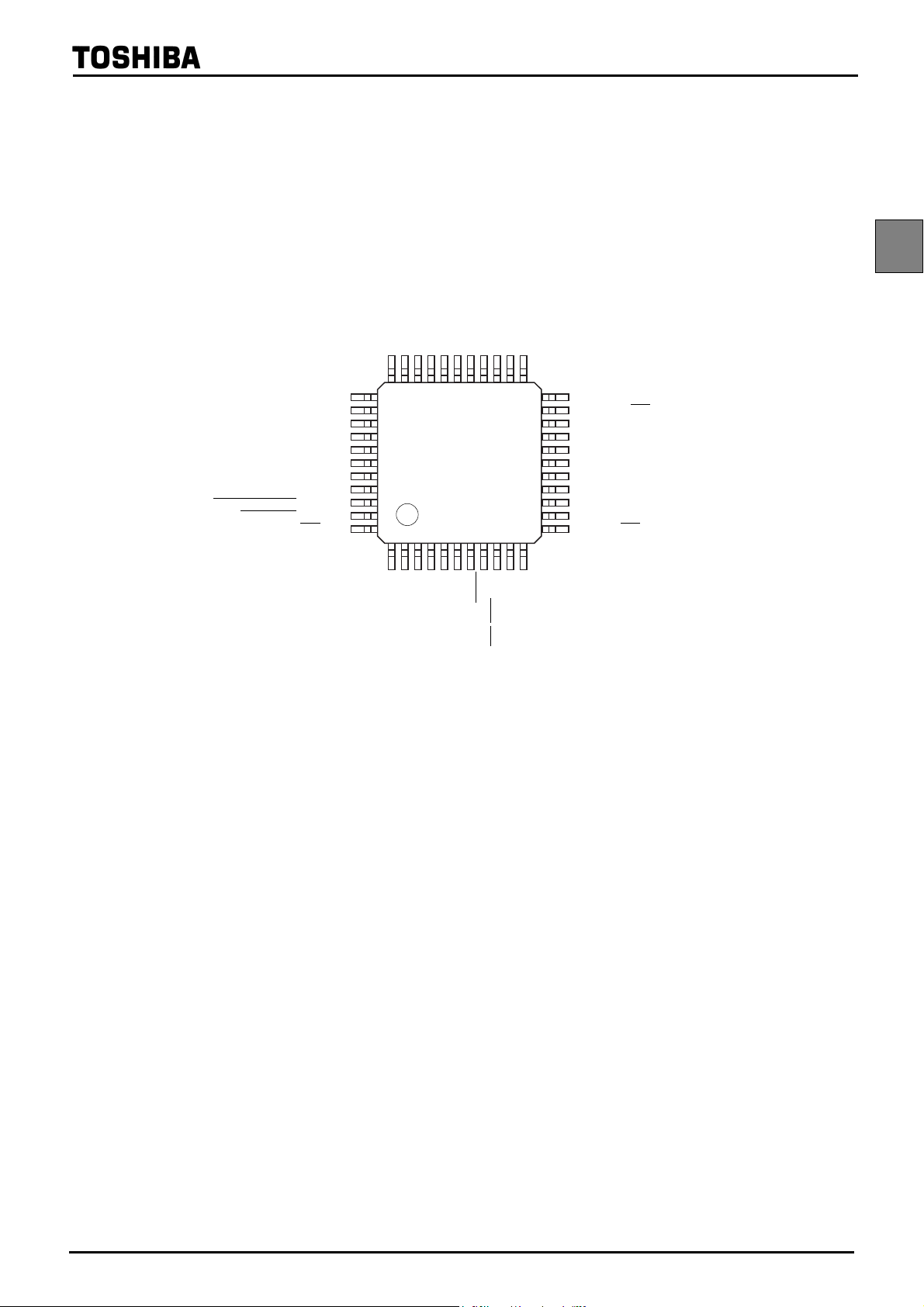
1.2 Pin Assignment
TMP86CH22UG
P52 (SEG21)
P51 (SEG22)
P53 (SEG20)
P55 (SEG18)
P56 (SEG17)
P70 (SEG15)
P73 (SEG12)
P57 (SEG16)
P72 (SEG13)
P71 (SEG14)
P54 (SEG19)
(SEG11) P74
(SEG10) P75
(SEG9) P76
COM3
COM2
COM1
COM0
VLC
(
PDO6/PWM6/PPG6/TC6) P33
PDO5/PWM5/TC5) P34
(
DVO) P37
(
3332313029282726252423
34
35
36
37
38
39
40
41
42
43
44
123456789
XIN
VSS
XOUT
VDD
TEST
(XTIN) P21
(XTOUT) P22
RESET
11
10
(INT5/STOP) P20
(ECIN/AIN1) P61
(ECNT/AIN2) P62
22
21
20
19
18
17
16
15
14
13
12
Figure 1-1 Pin Assignment
P50(SEG23)
P17(SEG24/
SCK)
P16(SEG25/SO)
P15(SEG26/SI)
P14(SEG27/INT3)
P13(SEG28/INT2)
P12(SEG29/INT1)
P11(SEG30/TXD)
P10(SEG31/RXD)
P64(AIN4/STOP2)
P63(AIN3/INT0)
Page 3
Page 15
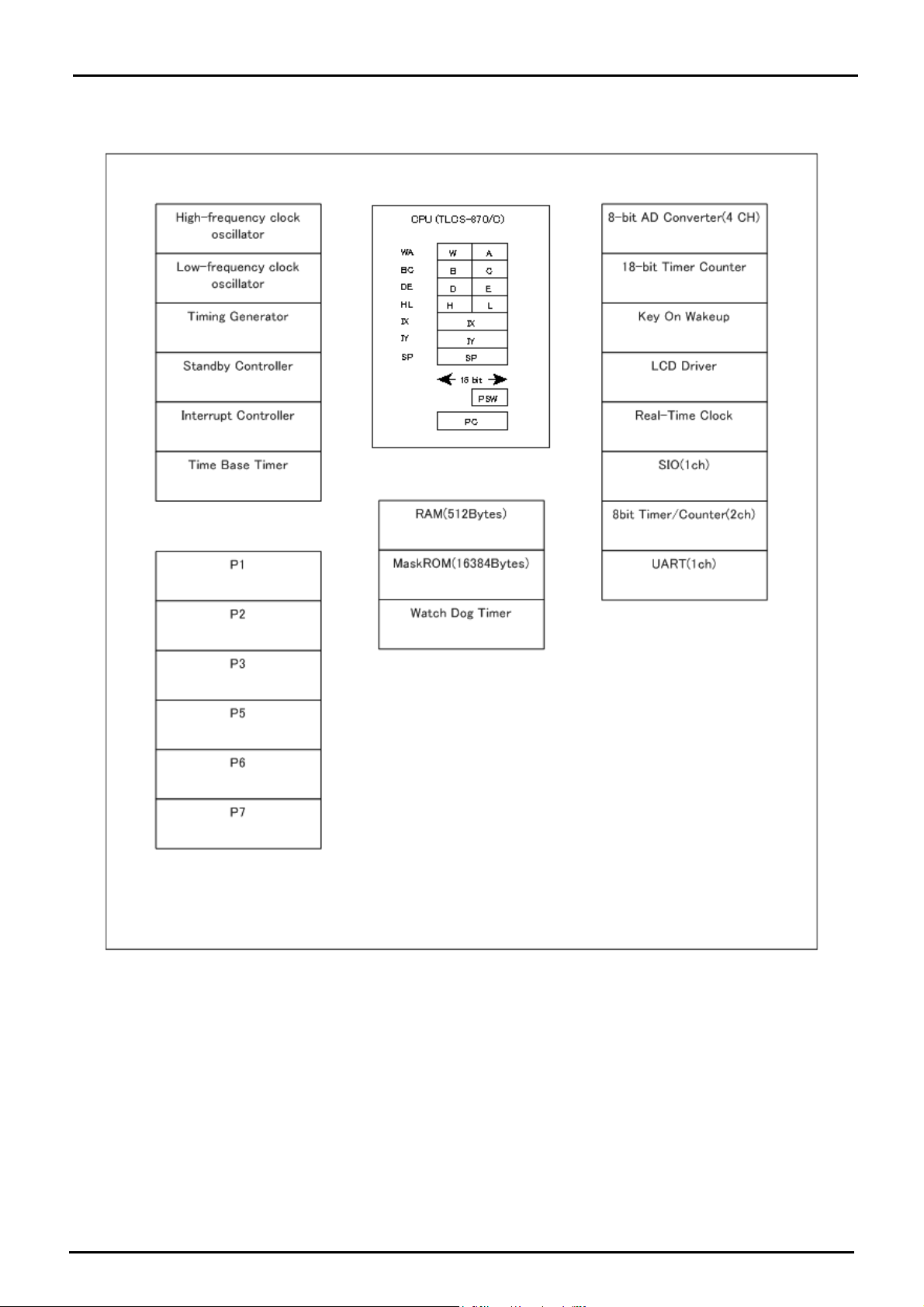
1.3 Block Diagram
1.3 Block Diagram
TMP86CH22UG
Figure 1-2 Block Diagram
Page 4
Page 16

1.4 Pin Names and Functions
Table 1-1 Pin Names and Functions(1/3)
Pin Name Pin Number Input/Output Functions
P17
SEG24
SCK
21
IO
PORT17
O
LCD segment output 24
IO
Serial Clock I/O
TMP86CH22UG
P16
SEG25
SO
P15
SEG26
SI
P14
SEG27
INT3
P13
SEG28
INT2
P12
SEG29
INT1
P11
SEG30
TXD
P10
SEG31
RXD
P22
XTOUT
IO
20
19
18
17
16
15
14
7
PORT16
O
LCD segment output 25
O
Serial Data Output
IO
PORT15
O
LCD segment output 26
I
Serial Data Input
IO
PORT14
O
LCD segment output 27
I
External interrupt 3 input
IO
PORT13
O
LCD segment output 28
I
External interrupt 2 input
IO
PORT12
O
LCD segment output 29
I
External interrupt 1 input
IO
PORT11
O
LCD segment output 30
I
UART data output
IO
PORT10
O
LCD segment output 31
I
UART data input
PORT22
IO
Resonator connecting pins(32.768kHz) for inputting external
O
clock
P21
XTIN
P20
STOP
INT5
P37
DVO
P34
TC5
PDO5/PWM5
P33
TC6
PDO6/PWM6/PPG6
P57
SEG16
P56
SEG17
P55
SEG18
PORT21
6
9
44
43
42
29
28
27
IO
Resonator connecting pins(32.768kHz) for inputting external
I
clock
IO
PORT20
I
STOP mode release signal input
I
External interrupt 5 input
OOPORT37
Divider Output
IO
PORT34
I
TC5 input
O
PDO5/PWM5 output
IO
PORT33
I
TC6 input
O
PDO6/PWM6/PPG6 output
IOOPORT57
LCD segment output 16
IOOPORT56
LCD segment output 17
IOOPORT55
LCD segment output 18
Page 5
Page 17

1.4 Pin Names and Functions
Table 1-1 Pin Names and Functions(2/3)
Pin Name Pin Number Input/Output Functions
TMP86CH22UG
P54
SEG19
P53
SEG20
P52
SEG21
P51
SEG22
P50
SEG23
P64
AIN4
STOP2
P63
AIN3
INT0
P62
AIN2
ECNT
P61
AIN1
ECIN
26
25
24
23
22
13
12
11
10
IOOPORT54
LCD segment output 19
IOOPORT53
LCD segment output 20
IOOPORT52
LCD segment output 21
IOOPORT51
LCD segment output 22
IOOPORT50
LCD segment output 23
IO
PORT64
I
AD converter analog input 4
I
STOP2 input
IO
PORT63
I
AD converter analog input 3
I
External interrupt 0 input
IO
PORT62
I
AD converter analog input 2
I
ECNT input
IO
PORT61
I
AD converter analog input 1
I
ECIN input
P76
SEG9
P75
SEG10
P74
SEG11
P73
SEG12
P72
SEG13
P71
SEG14
P70
SEG15
COM3 37 O LCD common output 3
COM2 38 O LCD common output 2
COM1 39 O LCD common output 1
COM0 40 O LCD common output 0
XIN 2 I Resonator connecting pins for high-frequency clock
36
35
34
33
32
31
30
IOOPORT76
LCD segment output 9
IOOPORT75
LCD segment output 10
IOOPORT74
LCD segment output 11
IOOPORT73
LCD segment output 12
IOIPORT72
LCD segment output 13
IOOPORT71
LCD segment output 14
IOOPORT70
LCD segment output 15
Page 6
Page 18

TMP86CH22UG
Table 1-1 Pin Names and Functions(3/3)
Pin Name Pin Number Input/Output Functions
XOUT 3 O Resonator connecting pins for high-frequency clock
RESET 8 I Reset signal
TEST 4 I Test pin for out-going test. Normally, be fixed to low.
VDD 5 I +5V
VSS 1 I 0(GND)
Page 7
Page 19

1.4 Pin Names and Functions
TMP86CH22UG
Page 8
Page 20
2. Operational Description
2.1 CPU Core Functions
The CPU core consists of a CPU, a system clock controller, and an interrupt controller.
This section provides a description of the CPU core, the program memory, the data memory, and the reset circuit.
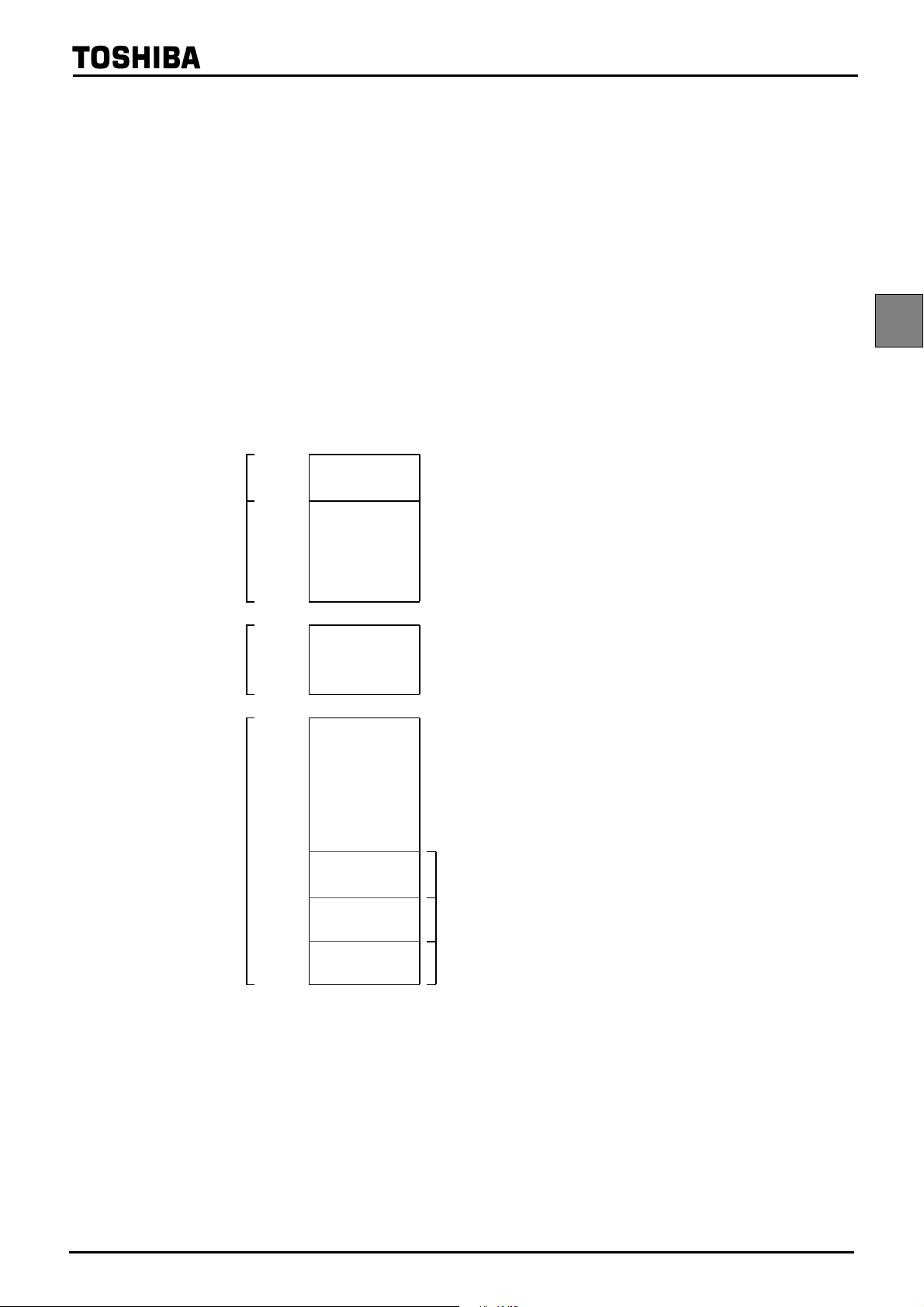
2.1.1 Memory Address Map
The TMP86CH22UG memory is composed MaskROM, RAM, DBR(Data buffer register) and SFR(Special
function register). They are all mapped in 64-Kbyte address space. Figure 2-1 shows the TMP86CH22UG
memory address map.
0000
SFR
RAM
003F
0040
023F
H
64 bytes
H
H
512
bytes
H
Special function register includes:
SFR:
I/O ports
Peripheral control registers
Peripheral status registers
System control registers
Program status word
Random access memory includes:
RAM:
Data memory
Stac k
TMP86CH22UG
0F80
H
DBR
MaskROM
0FFF
C000
FFB0
FFBF
FFC0
FFDF
FFE0
FFFF
H
H
H
H
H
H
H
H
128
bytes
16384
bytes
Figure 2-1 Memory Address Map
2.1.2 Program Memory (MaskROM)
DBR: Data buffer register includes:
Peripheral control registers
Peripheral status registers
LCD display memory
MaskROM:
Vector table for interrupts
(16 bytes)
Vector table for vector call instructions
(32 bytes)
Vector table for interrupts
(32 bytes)
Program memory
The TMP86CH22UG has a 16384 bytes (Address C000H to FFFFH) of program memory (MaskROM ).
Page 9
Page 21

2. Operational Description
2.2 System Clock Controller
2.1.3 Data Memory (RAM)
The TMP86CH22UG has 512bytes (Address 0040H to 023FH) of internal RAM. The first 192 bytes (0040H
to 00FFH) of the internal RAM are located in the direct area; instructions with shorten operations are available
against such an area.
The data memory contents become unstable when the power supply is turned on; therefore, the data memory
should be initialized by an initialization routine.
Example :Clears RAM to “00H”. (TMP86CH22UG)
SRAMCLR: LD (HL), A
TMP86CH22UG
LD HL, 0040H ; Start address setup
LD A, H ; Initial value (00H) setup
LD BC, 01FFH
INC HL
DEC BC
JRS F, SRAMCLR
2.2 System Clock Controller
The system clock controller consists of a clock generator, a timing generator, and a standby controller.
Clock
generator
XIN
High-frequency
clock oscillator
XOUT
XTIN
Low-frequency
clock oscillator
XTOUT
Figure 2-2 System Colck Control
2.2.1 Clock Generator
Timing generator control register
TBTCR
0036
H
fc
Timing
generator
fs
System clocks
Clock generator control
Standby controller
0038
H
0039
H
SYSCR2SYSCR1
System control registers
The clock generator generates the basic clock which provides the system clocks supplied to the CPU core
and peripheral hardware. It contains two oscillation circuits: One for the high-frequency clock and one for the
low-frequency clock. Power consumption can be reduced by switching of the standby controller to low-power
operation based on the low-frequency clock.
The high-frequency (fc) clock and low-frequency (fs) clock can easily be obtained by connecting a resonator
between the XIN/XOUT and XTIN/XTOUT pins respectively. Clock input from an external oscillator is also
possible. In this case, external clock is applied to XIN/XTIN pin with XOUT/XTOUT pin not connected.
Page 10
Page 22

TMP86CH22UG
(a) Crystal/Ceramic
resonator
Note:The function to monitor the basic clock directly at external is not provided for hardware, however, with dis-
abling all interrupts and watchdog timers, the oscillation frequency can be adjusted by monitoring the pulse
which the fixed frequency is outputted to the port by the program.
The system to require the adjustment of the oscillation frequency should create the program for the adjustment in advance.
High-frequency clock
XOUTXIN
(b) External oscillator
Figure 2-3 Examples of Resonator Connection
XOUTXIN
(Open)
Low-frequency clock
XTIN
(c) Crystal (d) External oscillator
XTOUT
XTIN
XTOUT
(Open)
Page 11
Page 23

2. Operational Description
2.2 System Clock Controller
2.2.2 Timing Generator
The timing generator generates the various system clocks supplied to the CPU core and peripheral hardware
from the basic clock (fc or fs). The timing generator provides the following functions.
2.2.2.1 Configuration of timing generator
1. Generation of main system clock
2. Generation of divider output (
DVO) pulses
3. Generation of source clocks for time base timer
4. Generation of source clocks for watchdog timer
5. Generation of internal source clocks for timer/counters
6. Generation of warm-up clocks for releasing STOP mode
7. LCD
TMP86CH22UG
SYSCK
DV7CK
High-frequency
clock fc
Low-frequency
clock fs
The timing generator consists of a 2-stage prescaler, a 21-stage divider, a main system clock generator,
and machine cycle counters.
An input clock to the 7th stage of the divider depends on the operating mode, SYSCR2<SYSCK> and
TBTCR<DV7CK>, that is shown in Figure 2-4. As reset and STOP mode started/canceled, the prescaler
and the divider are cleared to “0”.
fc or fs
S
fc/4
1 21 432 87 109 1211 1413 1615
5 6 17 18 19 20 21
A
Y
B
Multi-
plexer
Machine cycle countersMain system clock generator
Divider
B0
B1
A0
A1
S
Y0
Y1
Multiplexer
Warm-up
controller
Watchdog
timer
Timer counter, Serial interface, Time-base-timer, divider output, etc. (Peripheral functions)
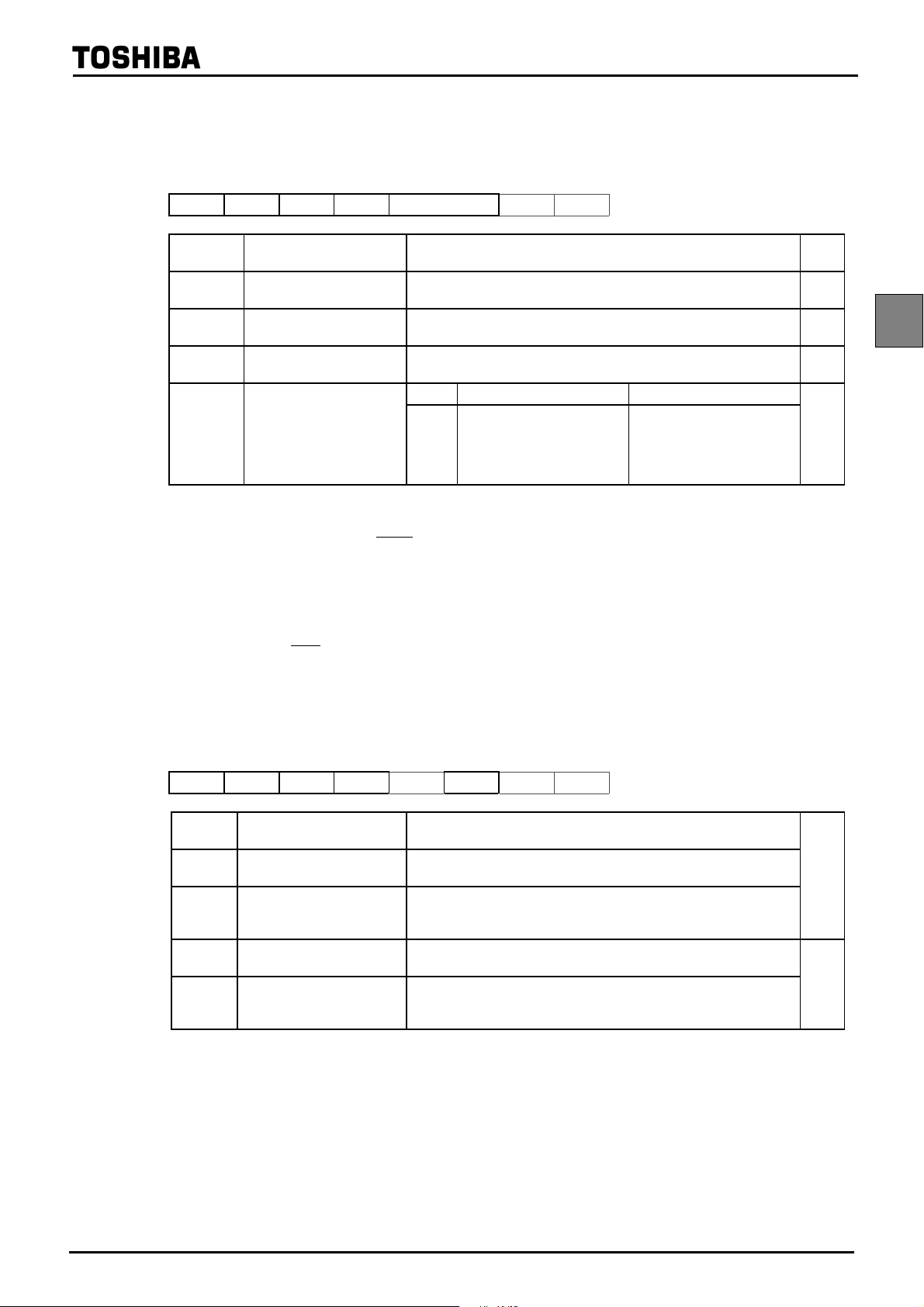
Figure 2-4 Configuration of Timing Generator
Page 12
Page 24
Timing Generator Control Register
TMP86CH22UG
TBTCR
(0036H)
Note 1: In single clock mode, do not set DV7CK to “1”.
Note 2: Do not set “1” on DV7CK while the low-frequency clock is not operated stably.
Note 3: fc: High-frequency clock [Hz], fs: Low-frequency clock [Hz], *: Don’t care
Note 4: In SLOW1/2 and SLEEP1/2 modes, the DV7CK setting is ineffective, and fs is input to the 7th stage of the divider.
Note 5: When STOP mode is entered from NORMAL1/2 mode, the DV7CK setting is ineffective during the warm-up period after
76543210
(DVOEN) (DVOCK) DV7CK (TBTEN) (TBTCK) (Initial value: 0000 0000)
DV7CK
release of STOP mode, and the 6th stage of the divider is input to the 7th stage during this period.
Selection of input to the 7th stage
of the divider
0: fc/2
1: fs
8
[Hz]
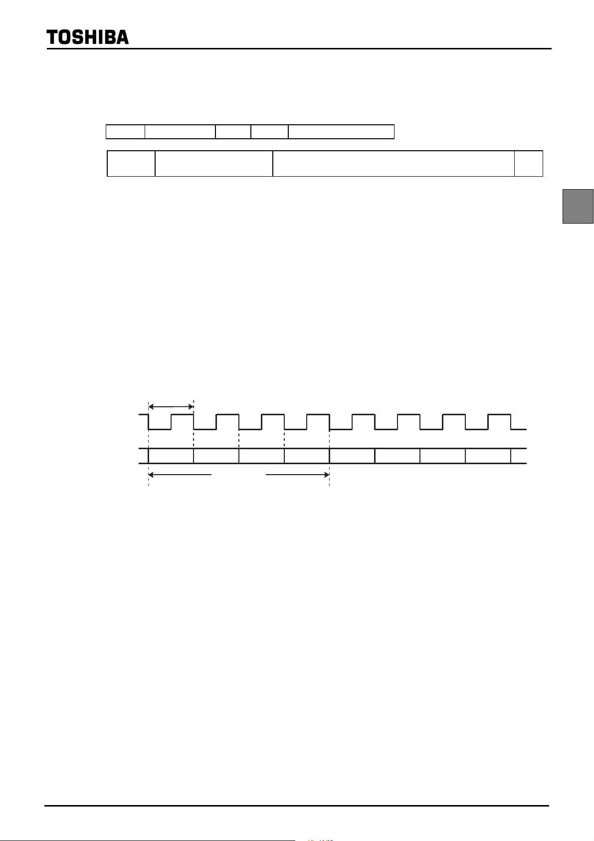
2.2.2.2 Machine cycle
Instruction execution and peripheral hardware operation are synchronized with the main system clock.
The minimum instruction execution unit is called an “machine cycle”. There are a total of 10 different
types of instructions for the TLCS-870/C Series: Ranging from 1-cycle instructions which require one
machine cycle for execution to 10-cycle instructions which require 10 machine cycles for execution. A
machine cycle consists of 4 states (S0 to S3), and each state consists of one main system clock.
1/fc or 1/fs [s]
R/W
Main system clock
State
Machine cycle
Figure 2-5 Machine Cycle
2.2.3 Operation Mode Control Circuit
The operation mode control circuit starts and stops the oscillation circuits for the high-frequency and lowfrequency clocks, and switches the main system clock. There are three operating modes: Single clock mode,
dual clock mode and STOP mode. These modes are controlled by the system control registers (SYSCR1 and
SYSCR2). Figure 2-6 shows the operating mode transition diagram.
2.2.3.1 Single-clock mode
Only the oscillation circuit for the high-frequency clock is used, and P21 (XTIN) and P22 (XTOUT)
pins are used as input/output ports. The main-system clock is obtained from the high-frequency clock. In
the single-clock mode, the machine cycle time is 4/fc [s].
S3S2S1S0 S3S2S1S0
(1) NORMAL1 mode
In this mode, both the CPU core and on-chip peripherals operate using the high-frequency clock.
The TMP86CH22UG is placed in this mode after reset.
Page 13
Page 25

2. Operational Description
2.2 System Clock Controller
TMP86CH22UG
(2) IDLE1 mode
In this mode, the internal oscillation circuit remains active. The CPU and the watchdog timer are
halted; however on-chip peripherals remain active (Operate using the high-frequency clock).
IDLE1 mode is started by SYSCR2<IDLE> = "1", and IDLE1 mode is released to NORMAL1
mode by an interrupt request from the on-chip peripherals or external interrupt inputs. When the IMF
(Interrupt master enable flag) is “1” (Interrupt enable), the execution will resume with the acceptance
of the interrupt, and the operation will return to normal after the interrupt service is completed. When
the IMF is “0” (Interrupt disable), the execution will resume with the instruction which follows the
IDLE1 mode start instruction.
(3) IDLE0 mode
In this mode, all the circuit, except oscillator and the timer-base-timer, stops operation.
This mode is enabled by SYSCR2<TGHALT> = "1".
When IDLE0 mode starts, the CPU stops and the timing generator stops feeding the clock to the
peripheral circuits other than TBT. Then, upon detecting the falling edge of the source clock selected
with TBTCR<TBTCK>, the timing generator starts feeding the clock to all peripheral circuits.
When returned from IDLE0 mode, the CPU restarts operating, entering NORMAL1 mode back
again. IDLE0 mode is entered and returned regardless of how TBTCR<TBTEN> is set. When IMF =
“1”, EF6 (TBT interrupt individual enable flag) = “1”, and TBTCR<TBTEN> = “1”, interrupt processing is performed. When IDLE0 mode is entered while TBTCR<TBTEN> = “1”, the INTTBT
interrupt latch is set after returning to NORMAL1 mode.
2.2.3.2 Dual-clock mode
Both the high-frequency and low-frequency oscillation circuits are used in this mode. P21 (XTIN) and
P22 (XTOUT) pins cannot be used as input/output ports. The main system clock is obtained from the
high-frequency clock in NORMAL2 and IDLE2 modes, and is obtained from the low-frequency clock in
SLOW and SLEEP modes. The machine cycle time is 4/fc [s] in the NORMAL2 and IDLE2 modes, and
4/fs [s] (122 µs at fs = 32.768 kHz) in the SLOW and SLEEP modes.
The TLCS-870/C is placed in the signal-clock mode during reset. To use the dual-clock mode, the lowfrequency oscillator should be turned on at the start of a program.
(1) NORMAL2 mode
In this mode, the CPU core operates with the high-frequency clock. On-chip peripherals operate
using the high-frequency clock and/or low-frequency clock.
(2) SLOW2 mode
In this mode, the CPU core operates with the low-frequency clock, while both the high-frequency
clock and the low-frequency clock are operated. As the SYSCR2<SYSCK> becomes "1", the hardware changes into SLOW2 mode. As the SYSCR2<SYSCK> becomes “0”, the hardware changes
into NORMAL2 mode. As the SYSCR2<XEN> becomes “0”, the hardware changes into SLOW1
mode. Do not clear SYSCR2<XTEN> to “0” during SLOW2 mode.
(3) SLOW1 mode
This mode can be used to reduce power-consumption by turning off oscillation of the high-frequency clock. The CPU core and on-chip peripherals operate using the low-frequency clock.
Page 14
Page 26

TMP86CH22UG
Switching back and forth between SLOW1 and SLOW2 modes are performed by
SYSCR2<XEN>. In SLOW1 and SLEEP modes, the input clock to the 1st stage of the divider is
stopped; output from the 1st to 6th stages is also stopped.
(4) IDLE2 mode
In this mode, the internal oscillation circuit remain active. The CPU and the watchdog timer are
halted; however, on-chip peripherals remain active (Operate using the high-frequency clock and/or
the low-frequency clock). Starting and releasing of IDLE2 mode are the same as for IDLE1 mode,
except that operation returns to NORMAL2 mode.
(5) SLEEP1 mode
In this mode, the internal oscillation circuit of the low-frequency clock remains active. The CPU,
the watchdog timer, and the internal oscillation circuit of the high-frequency clock are halted; however, on-chip peripherals remain active (Operate using the low-frequency clock). Starting and releasing of SLEEP mode are the same as for IDLE1 mode, except that operation returns to SLOW1 mode.
In SLOW1 and SLEEP1 modes, the input clock to the 1st stage of the divider is stopped; output from
the 1st to 6th stages is also stopped.
(6) SLEEP2 mode
The SLEEP2 mode is the idle mode corresponding to the SLOW2 mode. The status under the
SLEEP2 mode is same as that under the SLEEP1 mode, except for the oscillation circuit of the highfrequency clock.
(7) SLEEP0 mode
In this mode, all the circuit, except oscillator and the timer-base-timer, stops operation. This mode
is enabled by setting “1” on bit SYSCR2<TGHALT>.
When SLEEP0 mode starts, the CPU stops and the timing generator stops feeding the clock to the
peripheral circuits other than TBT. Then, upon detecting the falling edge of the source clock selected
with TBTCR<TBTCK>, the timing generator starts feeding the clock to all peripheral circuits.
When returned from SLEEP0 mode, the CPU restarts operating, entering SLOW1 mode back
again. SLEEP0 mode is entered and returned regardless of how TBTCR<TBTEN> is set. When IMF
= “1”, EF6 (TBT interrupt individual enable flag) = “1”, and TBTCR<TBTEN> = “1”, interrupt processing is performed. When SLEEP0 mode is entered while TBTCR<TBTEN> = “1”, the INTTBT
interrupt latch is set after returning to SLOW1 mode.
2.2.3.3 STOP mode
In this mode, the internal oscillation circuit is turned off, causing all system operations to be halted. The
internal status immediately prior to the halt is held with a lowest power consumption during STOP mode.
STOP mode is started by the system control register 1 (SYSCR1), and STOP mode is released by a
inputting (Either level-sensitive or edge-sensitive can be programmably selected) to the
STOP pin. After
the warm-up period is completed, the execution resumes with the instruction which follows the STOP
mode start instruction.
Page 15
Page 27
2. Operational Description
2.2 System Clock Controller
TMP86CH22UG
IDLE1
mode
(a) Single-clock mode
IDLE2
mode
SLEEP2
mode
SLEEP1
mode
(b) Dual-clock mode
SYSCR2<TGHALT> = "1"
SYSCR2<IDLE> = "1"
Interrupt
SYSCR2<XTEN> = "0"
SYSCR2<IDLE> = "1"
Interrupt
SYSCR2<SYSCK> = "0"
SYSCR2<IDLE> = "1"
Interrupt
SYSCR2<XEN> = "1"
SYSCR2<IDLE> = "1"
Interrupt
Note 2
IDLE0
mode
NORMAL1
mode
NORMAL2
mode
SLOW2
mode
SLOW1
mode
Reset release
Note 2
SYSCR1<STOP> = "1"
STOP pin input
SYSCR2<XTEN> = "1"
SYSCR1<STOP> = "1"
STOP pin input
SYSCR2<SYSCK> = "1"
SYSCR2<XEN> = "0"
SYSCR1<STOP> = "1"
STOP pin input
SYSCR2<TGHALT> = "1"
RESET
STOP
SLEEP0
mode
Note 1: NORMAL1 and NORMAL2 modes are generically called NORMAL; SLOW1 and SLOW2 are called SLOW; IDLE0, IDLE1
and IDLE2 are called IDLE; SLEEP0, SLEEP1 and SLEEP2 are called SLEEP.
Note 2: The mode is released by falling edge of TBTCR<TBTCK> setting.
Figure 2-6 Operating Mode Transition Diagram
Table 2-1 Operating Mode and Conditions
Operating Mode
Single clock
Dual clock
Oscillator
High
Frequency
RESET
NORMAL1 Operate
IDLE1
STOP Stop Halt –
NORMAL2
IDLE2 Halt
SLOW2
SLEEP2 Halt
SLOW1
SLEEP1
STOP Stop Halt –
Oscillation
Oscillation
Stop
Low
Frequency
Stop
Oscillation
CPU Core TBT
Reset Reset Reset
Operate
HaltIDLE0
Operate with
high frequency
Operate with
low frequency
Operate
Operate with
low frequency
HaltSLEEP0
Other
Peripherals
Operate
Halt
Operate
Halt
Machine Cycle
Time
4/fc [s]
4/fc [s]
4/fs [s]
Page 16
Page 28
System Control Register 1
SYSCR176543210
(0038H) STOP RELM RETM OUTEN WUT (Initial value: 0000 00**)
TMP86CH22UG
STOP STOP mode start
RELM
RETM
OUTEN Port output during STOP mode
WUT
Release method for STOP
mode
Operating mode after STOP
mode
Warm-up time at releasing
STOP mode
0: CPU core and peripherals remain active
1: CPU core and peripherals are halted (Start STOP mode)
0: Edge-sensitive release
1: Level-sensitive release
0: Return to NORMAL1/2 mode
1: Return to SLOW1 mode
0: High impedance
1: Output kept
Return to NORMAL mode Return to SLOW mode
00
01
10
11
3 x 2
2
3 x 2
2
16
/fc
16
/fc
14
/fc
14
/fc
3 x 2
2
3 x 2
R/W
R/W
R/W
R/W
13
/fs
13
/fs
6
/fs
6
/fs
2
R/W
Note 1: Always set RETM to “0” when transiting from NORMAL mode to STOP mode. Always set RETM to “1” when transiting
from SLOW mode to STOP mode.
Note 2: When STOP mode is released with
RESET pin input, a return is made to NORMAL1 regardless of the RETM contents.
Note 3: fc: High-frequency clock [Hz], fs: Low-frequency clock [Hz], *; Don’t care
Note 4: Bits 1 and 0 in SYSCR1 are read as undefined data when a read instruction is executed.
Note 5: As the hardware becomes STOP mode under OUTEN = “0”, input value is fixed to “0”; therefore it may cause external
interrupt request on account of falling edge.
Note 6: When the key-on wakeup is used, RELM should be set to "1".
Note 7: Port P20 is used as
STOP pin. Therefore, when stop mode is started, OUTEN does not affect to P20, and P20 becomes
High-Z mode.
Note 8: The warmig-up time should be set correctly for using oscillator.
System Control Register 2
SYSCR2
(0039H)
Note 1: A reset is applied if both XEN and XTEN are cleared to “0”, XEN is cleared to “0” when SYSCK = “0”, or XTEN is cleared
Note 2: *: Don’t care, TG: Timing generator, *; Don’t care
Note 3: Bits 3, 1 and 0 in SYSCR2 are always read as undefined value.
Note 4: Do not set IDLE and TGHALT to “1” simultaneously.
Note 5: Because returning from IDLE0/SLEEP0 to NORMAL1/SLOW1 is executed by the asynchronous internal clock, the period
Note 6: When IDLE1/2 or SLEEP1/2 mode is released, IDLE is automatically cleared to “0”.
Note 7: When IDLE0 or SLEEP0 mode is released, TGHALT is automatically cleared to “0”.
Note 8: Before setting TGHALT to “1”, be sure to stop peripherals. If peripherals are not stopped, the interrupt latch of peripherals
76543210
XEN XTEN SYSCK IDLE
XEN High-frequency oscillator control
XTEN Low-frequency oscillator control
Main system clock select
SYSCK
IDLE
TGHALT
(Write)/main system clock monitor (Read)
CPU and watchdog timer control
(IDLE1/2 and SLEEP1/2 modes)
TG control (IDLE0 and SLEEP0
modes)
TGHALT
0: Turn off oscillation
1: Turn on oscillation
0: Turn off oscillation
1: Turn on oscillation
0: High-frequency clock (NORMAL1/NORMAL2/IDLE1/IDLE2)
1: Low-frequency clock (SLOW1/SLOW2/SLEEP1/SLEEP2)
0: CPU and watchdog timer remain active
1: CPU and watchdog timer are stopped (Start IDLE1/2 and SLEEP1/2 modes)
0: Feeding clock to all peripherals from TG
1: Stop feeding clock to peripherals except TBT from TG.
(Start IDLE0 and SLEEP0 modes)
(Initial value: 1000 *0**)
to “0” when SYSCK = “1”.
of IDLE0/SLEEP0 mode might be shorter than the period setting by TBTCR<TBTCK>.
may be set after IDLE0 or SLEEP0 mode is released.
R/W
R/W
Page 17
Page 29

2. Operational Description
2.2 System Clock Controller
2.2.4 Operating Mode Control
2.2.4.1 STOP mode
TMP86CH22UG
STOP mode is controlled by the system control register 1, the STOP pin input and key-on wakeup input
(STOP2) which is controlled by the STOP mode release control register (STOPCR).
The
STOP pin is also used both as a port P20 and an INT5 (external interrupt input 5) pin. STOP mode is
started by setting SYSCR1<STOP> to “1”. During STOP mode, the following status is maintained.
1. Oscillations are turned off, and all internal operations are halted.
2. The data memory, registers, the program status word and port output latches are all held in the
status in effect before STOP mode was entered.
3. The prescaler and the divider of the timing generator are cleared to “0”.
4. The program counter holds the address 2 ahead of the instruction (e.g., [SET (SYSCR1).7])
which started STOP mode.
STOP mode includes a level-sensitive mode and an edge-sensitive mode, either of which can be
selected with the SYSCR1<RELM>. Do not use any key-on wakeup input (STOP2) for releasing STOP
mode in edge-sensitive mode.
Note 1: The STOP mode can be released by either the STOP or key-on wakeup pin (STOP2). However,
because the STOP pin is different from the key-on wakeup and can not inhibit the release input, the
STOP pin must be used for releasing STOP mode.
Note 2: During STOP period (from start of STOP mode to end of warm up), due to changes in the external
interrupt pin signal, interrupt latches may be set to “1” and interrupts may be accepted immediately
after STOP mode is released. Before starting STOP mode, therefore, disable interrupts. Also, before
enabling interrupts after STOP mode is released, clear unnecessary interrupt latches.
(1) Level-sensitive release mode (RELM = “1”)
In this mode, STOP mode is released by setting the
STOP pin high or setting the STOP2 pin input
which is enabled by STOPCR. This mode is used for capacitor backup when the main power supply
is cut off and long term battery backup.
Even if an instruction for starting STOP mode is executed while
input is low, STOP mode does not start but instead the warm-up sequence starts immediately. Thus,
to start STOP mode in the level-sensitive release mode, it is necessary for the program to first confirm that the
STOP pin input is low or STOP2 input is high. The following two methods can be used
for confirmation.
1. Testing a port.
2. Using an external interrupt input
INT5 (INT5 is a falling edge-sensitive input).
Example 1 :Starting STOP mode from NORMAL mode by testing a port P20.
STOP pin input is high or STOP2
LD (SYSCR1), 01010000B ; Sets up the level-sensitive release mode
SSTOPH: TEST (P2PRD). 0 ; Wait until the
JRS F, SSTOPH
DI ; IMF ← 0
SET (SYSCR1). 7 ; Starts STOP mode
Page 18
STOP pin input goes low level
Page 30
Example 2 :Starting STOP mode from NORMAL mode with an INT5 interrupt.
PINT5: TEST (P2PRD). 0 ; To reject noise, STOP mode does not start if
JRS F, SINT5 port P20 is at high
LD (SYSCR1), 01010000B ; Sets up the level-sensitive release mode.
DI ; IMF ← 0
SET (SYSCR1). 7 ; Starts STOP mode
SINT5: RETI
V
STOP pin
XOUT pin
IH
TMP86CH22UG
NORMAL
operation
Confirm by program that the
STOP pin input is low and start
STOP mode.
STOP
operation
Figure 2-7 Level-sensitive Release Mode
Note 1: Even if the STOP pin input is low after warm-up start, the STOP mode is not restarted.
Note 2: In this case of changing to the level-sensitive mode from the edge-sensitive mode, the release
mode is not switched until a rising edge of the
(2) Edge-sensitive release mode (RELM = “0”)
In this mode, STOP mode is released by a rising edge of the
cations where a relatively short program is executed repeatedly at periodic intervals. This periodic
signal (for example, a clock from a low-power consumption oscillator) is input to the
the edge-sensitive release mode, STOP mode is started even when the
Do not use any STOP2 pin input for releasing STOP mode in edge-sensitive release mode.
Example :Starting STOP mode from NORMAL mode
Warm up
STOP mode is released by the hardware.
Always released if the STOP
pin input is high.
STOP pin input is detected.
NORMAL
operation
STOP pin input. This is used in appli-
STOP pin input is high level.
STOP pin. In
STOP pin
XOUT pin
STOP mode started
by the program.
DI ; IMF ← 0
LD (SYSCR1), 10010000B ; Starts after specified to the edge-sensitive release mode
V
IH
NORMAL
operation
STOP
operation
Warm up
STOP mode is released by the hardware at the rising
edge of STOP pin input.
NORMAL
operation
Figure 2-8 Edge-sensitive Release Mode
Page 19
STOP
operation
Page 31

2. Operational Description
2.2 System Clock Controller
TMP86CH22UG
STOP mode is released by the following sequence.
1. In the dual-clock mode, when returning to NORMAL2, both the high-frequency and lowfrequency clock oscillators are turned on; when returning to SLOW1 mode, only the lowfrequency clock oscillator is turned on. In the single-clock mode, only the high-frequency
clock oscillator is turned on.
2. A warm-up period is inserted to allow oscillation time to stabilize. During warm up, all
internal operations remain halted. Four different warm-up times can be selected with the
SYSCR1<WUT> in accordance with the resonator characteristics.
3. When the warm-up time has elapsed, normal operation resumes with the instruction following the STOP mode start instruction.
Note 1: When the STOP mode is released, the start is made after the prescaler and the divider of the
timing generator are cleared to "0".
Note 2: STOP mode can also be released by inputting low level on the
performs the normal reset operation.
Note 3: When STOP mode is released with a low hold voltage, the following cautions must be observed.
The power supply voltage must be at the operating voltage level before releasing STOP mode.
The
RESET pin input must also be “H” level, rising together with the power supply voltage. In this
case, if an external time constant circuit has been connected, the
increase at a slower pace than the power supply voltage. At this time, there is a danger that a
reset may occur if input voltage level of the
input voltage (Hysteresis input).
RESET pin drops below the non-inverting high-level
RESET pin, which immediately
RESET pin input voltage will
Table 2-2 Warm-up Time Example (at fc = 16.0 MHz, fs = 32.768 kHz)
WUT
00
01
10
11
Note 1: The warm-up time is obtained by dividing the basic clock by the divider. Therefore, the warm-up
time may include a certain amount of error if there is any fluctuation of the oscillation frequency
when STOP mode is released. Thus, the warm-up time must be considered as an approximate
value.
Return to NORMAL Mode Return to SLOW Mode
12.288
4.096
3.072
1.024
Warm-up Time [ms]
750
250
5.85
1.95
Page 20
Page 32

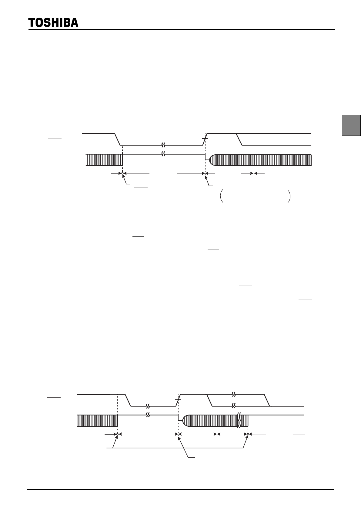
Turn off
TMP86CH22UG
a + 3
Halt
0n
n + 2 n + 3 n + 4
a + 6
Instruction address a + 4
a + 5
Instruction address a + 3
a + 4
Instruction address a + 2
3
2
1
(b) STOP mode release
0
Turn on
Oscillator
circuit
Main
system
clock
a + 2
Program
counter
Instruction
SET (SYSCR1). 7
(a) STOP mode start (Example: Start with SET (SYSCR1). 7 instruction located at address a)
n + 1
Warm up
Turn on
Turn off
execution
Divider
STOP pin
input
Oscillator
circuit
Main
Figure 2-9 STOP Mode Start/Release
system
clock
a + 3
Halt
Program
counter
Count up
0
Instruction
execution
Divider
Page 21
Page 33

2. Operational Description
2.2 System Clock Controller
2.2.4.2 IDLE1/2 mode and SLEEP1/2 mode
TMP86CH22UG
IDLE1/2 and SLEEP1/2 modes are controlled by the system control register 2 (SYSCR2) and maskable
interrupts. The following status is maintained during these modes.
1. Operation of the CPU and watchdog timer (WDT) is halted. On-chip peripherals continue to
operate.
2. The data memory, CPU registers, program status word and port output latches are all held in the
status in effect before these modes were entered.
3. The program counter holds the address 2 ahead of the instruction which starts these modes.
Starting IDLE1/2 and
SLEEP1/2 modes by
instruction
CPU and WDT are halted
Normal
release mode
Reset input
No
No
Interrupt request
Yes
“0”
Execution of the instruc-
tion which follows the
IDLE1/2 and SLEEP1/2
modes start instruction
IMF
Interrupt processing
Yes
“1” (Interrupt release mode)
Reset
Figure 2-10 IDLE1/2 and SLEEP1/2 Modes
Page 22
Page 34

TMP86CH22UG
• Start the IDLE1/2 and SLEEP1/2 modes
After IMF is set to "0", set the individual interrupt enable flag (EF) which releases IDLE1/2
and SLEEP1/2 modes. To start IDLE1/2 and SLEEP1/2 modes, set SYSCR2<IDLE> to “1”.
• Release the IDLE1/2 and SLEEP1/2 modes
IDLE1/2 and SLEEP1/2 modes include a normal release mode and an interrupt release mode.
These modes are selected by interrupt master enable flag (IMF). After releasing IDLE1/2 and
SLEEP1/2 modes, the SYSCR2<IDLE> is automatically cleared to “0” and the operation mode
is returned to the mode preceding IDLE1/2 and SLEEP1/2 modes.
IDLE1/2 and SLEEP1/2 modes can also be released by inputting low level on the
RESET pin.
After releasing reset, the operation mode is started from NORMAL1 mode.
(1) Normal release mode (IMF = “0”)
IDLE1/2 and SLEEP1/2 modes are released by any interrupt source enabled by the individual
interrupt enable flag (EF). After the interrupt is generated, the program operation is resumed from the
instruction following the IDLE1/2 and SLEEP1/2 modes start instruction. Normally, the interrupt
latches (IL) of the interrupt source used for releasing must be cleared to “0” by load instructions.
(2) Interrupt release mode (IMF = “1”)
IDLE1/2 and SLEEP1/2 modes are released by any interrupt source enabled with the individual
interrupt enable flag (EF) and the interrupt processing is started. After the interrupt is processed, the
program operation is resumed from the instruction following the instruction, which starts IDLE1/2
and SLEEP1/2 modes.
Note: When a watchdog timer interrupts is generated immediately before IDLE1/2 and SLEEP1/2
modes are started, the watchdog timer interrupt will be processed but IDLE1/2 and SLEEP1/2
modes will not be started.
Page 23
Page 35

2. Operational Description
2.2 System Clock Controller
TMP86CH22UG
Halt
a + 3
a + 2
Operate
SET (SYSCR2). 4
(a) IDLE1/2 and SLEEP1/2 modes start (Example: Starting with the SET instruction located at address a)
a + 4 a + 3
Instruction address a + 2
Operate
Halt
Halt
㽲㩷Normal release mode
Acceptance of interrupt
a + 3
Halt
Halt
Operate
Operate
(b) IDLE1/2 and SLEEP1/2 modes release
㽳㩷Interrupt release mode
Main
system
clock
Interrupt
request
Program
counter
Instruction
execution
Watchdog
timer
Main
system
clock
Interrupt
request
Program
counter
Instruction
execution
Watchdog
timer
Main
system
clock
Interrupt
request
Program
counter
Figure 2-11 IDLE1/2 and SLEEP1/2 Modes Start/Release
Page 24
Instruction
execution
Watchdog
timer
Page 36

2.2.4.3 IDLE0 and SLEEP0 modes (IDLE0, SLEEP0)
IDLE0 and SLEEP0 modes are controlled by the system control register 2 (SYSCR2) and the time base
timer control register (TBTCR). The following status is maintained during IDLE0 and SLEEP0 modes.
1. Timing generator stops feeding clock to peripherals except TBT.
2. The data memory, CPU registers, program status word and port output latches are all held in the
status in effect before IDLE0 and SLEEP0 modes were entered.
3. The program counter holds the address 2 ahead of the instruction which starts IDLE0 and
SLEEP0 modes.
Note: Before starting IDLE0 or SLEEP0 mode, be sure to stop (Disable) peripherals.
Stopping peripherals
by instruction
Starting IDLE0, SLEEP0
modes by instruction
TMP86CH22UG
(Normal release mode)
CPU and WDT are halted
Reset input
No
No
No
No
No
TBT
source clock
falling
edge
Yes
TBTCR<TBTEN>
= "1"
Yes
TBT interrupt
enable
Yes
IMF = "1"
Yes (Interrupt release mode)
Interrupt processing
Yes
Reset
Execution of the instruction
which follows the IDLE0,
SLEEP0 modes start
instruction
Figure 2-12 IDLE0 and SLEEP0 Modes
Page 25
Page 37

2. Operational Description
2.2 System Clock Controller
TMP86CH22UG
• Start the IDLE0 and SLEEP0 modes
Stop (Disable) peripherals such as a timer counter.
To start IDLE0 and SLEEP0 modes, set SYSCR2<TGHALT> to “1”.
• Release the IDLE0 and SLEEP0 modes
IDLE0 and SLEEP0 modes include a normal release mode and an interrupt release mode.
These modes are selected by interrupt master flag (IMF), the individual interrupt enable flag
of TBT and TBTCR<TBTEN>.
After releasing IDLE0 and SLEEP0 modes, the SYSCR2<TGHALT> is automatically
cleared to “0” and the operation mode is returned to the mode preceding IDLE0 and SLEEP0
modes. Before starting the IDLE0 or SLEEP0 mode, when the TBTCR<TBTEN> is set to “1”,
INTTBT interrupt latch is set to “1”.
IDLE0 and SLEEP0 modes can also be released by inputting low level on the
RESET pin.
After releasing reset, the operation mode is started from NORMAL1 mode.
Note: IDLE0 and SLEEP0 modes start/release without reference to TBTCR<TBTEN> setting.
(1) Normal release mode (IMF•EF6•TBTCR<TBTEN> = “0”)
IDLE0 and SLEEP0 modes are released by the source clock falling edge, which is setting by the
TBTCR<TBTCK>. After the falling edge is detected, the program operation is resumed from the
instruction following the IDLE0 and SLEEP0 modes start instruction. Before starting the IDLE0 or
SLEEP0 mode, when the TBTCR<TBTEN> is set to “1”, INTTBT interrupt latch is set to “1”.
(2) Interrupt release mode (IMF•EF6•TBTCR<TBTEN> = “1”)
IDLE0 and SLEEP0 modes are released by the source clock falling edge, which is setting by the
TBTCR<TBTCK> and INTTBT interrupt processing is started.
Note 1: Because returning from IDLE0, SLEEP0 to NORMAL1, SLOW1 is executed by the asynchro-
nous internal clock, the period of IDLE0, SLEEP0 mode might be the shorter than the period setting by TBTCR<TBTCK>.
Note 2: When a watchdog timer interrupt is generated immediately before IDLE0/SLEEP0 mode is
started, the watchdog timer interrupt will be processed but IDLE0/SLEEP0 mode will not be
started.
Page 26
Page 38

a + 3
TMP86CH22UG
Halt
a + 2
SET (SYSCR2). 2
Operate
(a) IDLE0 and SLEEP0 modes start (Example: Starting with the SET instruction located at address a
a + 4 a + 3
Instruction address a + 2
Operate
Halt
Halt
㽲㩷Normal release mode
Acceptance of interrupt
a + 3
Halt
Halt
Operate
㽳㩷Interrupt release mode
(b) IDLE and SLEEP0 modes release
system
clock
Interrupt
request
Program
counter
Instruction
execution
Watchdog
timer
Main
system
clock
TBT clock
Program
counter
Instruction
execution
Watchdog
timer
Figure 2-13 IDLE0 and SLEEP0 Modes Start/Release
Page 27
Main
system
clock
TBT clock
Program
counter
Instruction
execution
Watchdog
timer
Page 39

2. Operational Description
2.2 System Clock Controller
2.2.4.4 SLOW mode
Example 1 :Switching from NORMAL2 mode to SLOW1 mode.
TMP86CH22UG
SLOW mode is controlled by the system control register 2 (SYSCR2).
The following is the methods to switch the mode with the warm-up counter.
(1) Switching from NORMAL2 mode to SLOW1 mode
First, set SYSCR2<SYSCK> to switch the main system clock to the low-frequency clock for
SLOW2 mode. Next, clear SYSCR2<XEN> to turn off high-frequency oscillation.
Note: The high-frequency clock can be continued oscillation in order to return to NORMAL2 mode from
SLOW mode quickly. Always turn off oscillation of high-frequency clock when switching from
SLOW mode to stop mode.
SET (SYSCR2). 5
CLR (SYSCR2). 7
; SYSCR2<SYSCK>
(Switches the main system clock to the low-frequency
clock for SLOW2)
; SYSCR2<XEN>
(Turns off high-frequency oscillation)
← 1
← 0
Example 2 :Switching to the SLOW1 mode after low-frequency clock has stabilized.
SET (SYSCR2). 6
LD (TC5CR), 43H ; Sets mode for TC6, 5 (16-bit mode, fs for source)
LD (TC6CR), 05H ; Sets warming-up counter mode
LDW (TTREG5), 8000H ; Sets warm-up time (Depend on oscillator accompanied)
DI
SET (EIRH). 5 ; Enables INTTC6
EI
SET (TC6CR). 3 ; Starts TC6, 5
:
PINTTC6: CLR (TC6CR). 3 ; Stops TC6, 5
; SYSCR2<XTEN>
← 0
; IMF
← 1
; IMF
← 1
SET (SYSCR2). 5
CLR (SYSCR2). 7
RETI
:
VINTTC6: DW PINTTC6 ; INTTC6 vector table
; SYSCR2<SYSCK>
(Switches the main system clock to the low-frequency clock)
; SYSCR2<XEN>
(Turns off high-frequency oscillation)
← 0
Page 28
← 1
Page 40

TMP86CH22UG
(2) Switching from SLOW1 mode to NORMAL2 mode
First, set SYSCR2<XEN> to turn on the high-frequency oscillation. When time for stabilization
(Warm up) has been taken by the timer/counter (TC
6,TC5), clear SYSCR2<SYSCK> to switch the
main system clock to the high-frequency clock.
SLOW mode can also be released by inputting low level on the
RESET pin. After releasing reset, the
operation mode is started from NORMAL1 mode.
Note: After SYSCK is cleared to “0”, executing the instructions is continiued by the low-frequency clock
for the period synchronized with low-frequency and high-frequency clocks.
High-frequency clock
Low-frequency clock
Main system clock
SYSCK
Example :Switching from the SLOW1 mode to the NORMAL2 mode (fc = 16 MHz, warm-up time is 4.0 ms).
SET (SYSCR2). 7
LD (TC5CR), 63H ; Sets mode for TC6, 5 (16-bit mode, fc for source)
LD (TC6CR), 05H ; Sets warming-up counter mode
LD (TTREG6), 0F8H ; Sets warm-up time
DI
SET (EIRH). 5 ; Enables INTTC6
EI
SET (TC6CR). 3 ; Starts TC6, 5
:
PINTTC6: CLR (TC6CR). 3 ; Stops TC6, 5
CLR (SYSCR2). 5
RETI
:
VINTTC6: DW PINTTC6 ; INTTC6 vector table
; SYSCR2<XEN>
← 0
; IMF
← 1
; IMF
; SYSCR2<SYSCK>
(Switches the main system clock to the high-frequency clock)
← 1 (Starts high-frequency oscillation)
← 0
Page 29
Page 41

2. Operational Description
2.2 System Clock Controller
Turn off
SLOW1 mode
TMP86CH22UG
NORMAL2
mode
CLR (SYSCR2). 7
SLOW2 mode
(a) Switching to the SLOW mode
SET (SYSCR2). 5
CLR (SYSCR2). 5
Warm up during SLOW2 mode
(b) Switching to the NORMAL2 mode
NORMAL2
mode
High-
frequency
clock
Low-
frequency
clock
Main
system
clock
SYSCK
XEN
Instruction
execution
High-
frequency
clock
Low-
frequency
clock
Main
system
clock
SYSCK
Figure 2-14 Switching between the NORMAL2 and SLOW Modes
Page 30
XEN
Instruction
SET (SYSCR2). 7
SLOW1 mode
execution
Page 42

TMP86CH22UG
2.3 Reset Circuit
The TMP86CH22UG has four types of reset generation procedures: An external reset input, an address trap reset,
a watchdog timer reset and a system clock reset. Of these reset, the address trap reset, the watchdog timer and the
system clock reset are a malfunction reset. When the malfunction reset request is detected, reset occurs during the
maximum 24/fc[s].
The malfunction reset circuit such as watchdog timer reset, address trap reset and system clock reset is not initialized when power is turned on. Therefore, reset may occur during maximum 24/fc[s] (1.5µs at 16.0 MHz) when
power is turned on.
Table 2-3 shows on-chip hardware initialization by reset action.
Table 2-3 Initializing Internal Status by Reset Action
On-chip Hardware Initial Value On-chip Hardware Initial Value
Program counter (PC) (FFFEH)
Stack pointer (SP) Not initialized
General-purpose registers
(W, A, B, C, D, E, H, L, IX, IY)
Jump status flag (JF) Not initialized Watchdog timer Enable
Zero flag (ZF) Not initialized
Carry flag (CF) Not initialized
Half carry flag (HF) Not initialized
Sign flag (SF) Not initialized
Overflow flag (VF) Not initialized
Interrupt master enable flag (IMF) 0
Interrupt individual enable flags (EF) 0
Interrupt latches (IL) 0
Not initialized
Prescaler and divider of timing generator 0
Output latches of I/O ports Refer to I/O port circuitry
Control registers
LCD data buffer Not initialized
RAM Not initialized
Refer to each of control
register
2.3.1 External Reset Input
The RESET pin contains a Schmitt trigger (Hysteresis) with an internal pull-up resistor.
When the
age within the operating voltage range and oscillation stable, a reset is applied and the internal state is initialized.
When the
vector address stored at addresses FFFEH to FFFFH.
RESET
RESET pin is held at “L” level for at least 3 machine cycles (12/fc [s]) with the power supply volt-
RESET pin input goes high, the reset operation is released and the program execution starts at the
VDD
Internal reset
Malfunction
reset output
circuit
Figure 2-15 Reset Circuit
Watchdog timer reset
Address trap reset
System clock reset
Page 31
Page 43

2. Operational Description
2.3 Reset Circuit
2.3.2 Address trap reset
If the CPU should start looping for some cause such as noise and an attempt be made to fetch an instruction
from the on-chip RAM (when WDTCR1<ATAS> is set to “1”), DBR or the SFR area, address trap reset will be
generated. The reset time is maximum 24/fc[s] (1.5µs at 16.0 MHz).
Note:The operating mode under address trapped is alternative of reset or interrupt. The address trap area is alter-
Instruction
execution
Internal reset
native.
JP a
Address trap is occurred
Reset release
TMP86CH22UG
Instruction at address r
4/fc to 12/fc [s]
Note 1: Address “a” is in the SFR, DBR or on-chip RAM (WDTCR1<ATAS> = “1”) space.
Note 2: During reset release, reset vector “r” is read out, and an instruction at address “r” is fetched and decoded.
16/fc [s] maximum 24/fc [s]
Figure 2-16 Address Trap Reset
2.3.3 Watchdog timer reset
Refer to Section “Watchdog Timer”.
2.3.4 System clock reset
If the condition as follows is detected, the system clock reset occurs automatically to prevent dead lock of the
CPU. (The oscillation is continued without stopping.)
- In case of clearing SYSCR2<XEN> and SYSCR2<XTEN> simultaneously to “0”.
- In case of clearing SYSCR2<XEN> to “0”, when the SYSCR2<SYSCK> is “0”.
- In case of clearing SYSCR2<XTEN> to “0”, when the SYSCR2<SYSCK> is “1”.
The reset time is maximum 24/fc (1.5 µs at 16.0 MHz).
Page 32
Page 44

TMP86CH22UG
Page 33
Page 45

2. Operational Description
2.3 Reset Circuit
TMP86CH22UG
Page 34
Page 46

TMP86CH22UG
3. Interrupt Control Circuit
The TMP86CH22UG has a total of 18 interrupt sources excluding reset. Interrupts can be nested with priorities.
Four of the internal interrupt sources are non-maskable while the rest are maskable.
Interrupt sources are provided with interrupt latches (IL), which hold interrupt requests, and independent vectors.
The interrupt latch is set to “1” by the generation of its interrupt request which requests the CPU to accept its interrupts. Interrupts are enabled or disabled by software using the interrupt master enable flag (IMF) and interrupt enable
flag (EF). If more than one interrupts are generated simultaneously, interrupts are accepted in order which is dominated by hardware. However, there are no prioritized interrupt factors among non-maskable interrupts.
Interrupt Factors Enable Condition
Internal/External (Reset) Non-maskable – FFFE 1
Internal INTSWI (Software interrupt) Non-maskable – FFFC 2
Internal
Internal INTATRAP (Address trap interrupt) Non-maskable IL2 FFFA 2
Internal INTWDT (Watchdog timer interrupt) Non-maskable IL3 FFF8 2
External
External INT1 IMF• EF5 = 1 IL5 FFF4 6
Internal INTTBT IMF• EF6 = 1 IL6 FFF2 7
Internal INTTC1 IMF• EF7 = 1 IL7 FFF0 8
Internal INTSIO IMF• EF8 = 1 IL8 FFEE 9
External INT2 IMF• EF9 = 1 IL9 FFEC 10
Internal INTRXD IMF• EF10 = 1 IL10 FFEA 11
Internal INTTXD IMF• EF11 = 1 IL11 FFE8 12
- Reserved IMF• EF12 = 1 IL12 FFE6 13
Internal INTTC6 IMF• EF13 = 1 IL13 FFE4 14
Internal INTRTC IMF• EF14 = 1 IL14 FFE2 15
Internal INTADC IMF• EF15 = 1 IL15 FFE0 16
- Reserved IMF• EF16 = 1 IL16 FFBE 17
External INT3 IMF• EF17 = 1 IL17 FFBC 18
Internal INTTC5 IMF• EF18 = 1 IL18 FFBA 19
External
- Reserved IMF• EF20 = 1 IL20 FFB6 21
- Reserved IMF• EF21 = 1 IL21 FFB4 22
- Reserved IMF• EF22 = 1 IL22 FFB2 23
- Reserved IMF• EF23 = 1 IL23 FFB0 24
INTUNDEF (Executed the undefined instruction
interrupt)
INT0 IMF• EF4 = 1, INT0EN = 1 IL4 FFF6 5
INT5 IMF• EF19 = 1 IL19 FFB8 20
Non-maskable – FFFC 2
Interrupt
Latch
Vector
Address
Priority
Note 1: To use the address trap interrupt (INTATRAP), clear WDTCR1<ATOUT> to “0” (It is set for the “reset request” after reset is
cancelled). For details, see “Address Trap”.
Note 2: To use the watchdog timer interrupt (INTWDT), clear WDTCR1<WDTOUT> to "0" (It is set for the "Reset request" after
reset is released). For details, see "Watchdog Timer".
Note 3: If an INTADC interrupt request is generated while an interrupt with priority lower than the interrupt latch IL15 (INTADC) is
being accepted, the INTADC interrupt latch may be cleared without the INTADC interrupt being processed. For details,
refer to the corresponding notes in the chapter on the AD converter.
3.1 Interrupt latches (IL19 to IL2)
An interrupt latch is provided for each interrupt source, except for a software interrupt and an executed the undefined instruction interrupt. When interrupt request is generated, the latch is set to “1”, and the CPU is requested to
accept the interrupt if its interrupt is enabled. The interrupt latch is cleared to "0" immediately after accepting interrupt. All interrupt latches are initialized to “0” during reset.
Page 35
Page 47

3. Interrupt Control Circuit
3.2 Interrupt enable register (EIR)
The interrupt latches are located on address 002EH, 003CH and 003DH in SFR area. Each latch can be cleared to
"0" individually by instruction. However, IL2 and IL3 should not be cleared to "0" by software. For clearing the
interrupt latch, load instruction should be used and then IL2 and IL3 should be set to "1". If the read-modify-write
instructions such as bit manipulation or operation instructions are used, interrupt request would be cleared inadequately if interrupt is requested while such instructions are executed.
Interrupt latches are not set to “1” by an instruction.
Since interrupt latches can be read, the status for interrupt requests can be monitored by software.
Note: In main program, before manipulating the interrupt enable flag (EF) or the interrupt latch (IL), be sure to clear IMF to
"0" (Disable interrupt by DI instruction). Then set IMF newly again as required after operating on the EF or IL
(Enable interrupt by EI instruction)
In interrupt service routine, because the IMF becomes "0" automatically, clearing IMF need not execute normally on
interrupt service routine. However, if using multiple interrupt on interrupt service routine, manipulating EF or IL
should be executed before setting IMF="1".
Example 1 :Clears interrupt latches
TMP86CH22UG
DI
LDW (ILL), 1110100000111111B
EI
← 0
; IMF
; IL12, IL10 to IL6
; IMF
← 1
← 0
Example 2 :Reads interrupt latchess
LD WA, (ILL)
← ILH, A ← ILL
; W
Example 3 :Tests interrupt latches
TEST (ILL). 7 ; if IL7 = 1 then jump
JR F, SSET
3.2 Interrupt enable register (EIR)
The interrupt enable register (EIR) enables and disables the acceptance of interrupts, except for the non-maskable
interrupts (Software interrupt, undefined instruction interrupt, address trap interrupt and watchdog interrupt). Nonmaskable interrupt is accepted regardless of the contents of the EIR.
The EIR consists of an interrupt master enable flag (IMF) and the individual interrupt enable flags (EF). These
registers are located on address 002CH, 003AH and 003BH in SFR area, and they can be read and written by an
instructions (Including read-modify-write instructions such as bit manipulation or operation instructions).
3.2.1 Interrupt master enable flag (IMF)
The interrupt enable register (IMF) enables and disables the acceptance of the whole maskable interrupt.
While IMF = “0”, all maskable interrupts are not accepted regardless of the status on each individual interrupt
enable flag (EF). By setting IMF to “1”, the interrupt becomes acceptable if the individuals are enabled. When
an interrupt is accepted, IMF is cleared to “0” after the latest status on IMF is stacked. Thus the maskable interrupts which follow are disabled. By executing return interrupt instruction [RETI/RETN], the stacked data,
which was the status before interrupt acceptance, is loaded on IMF again.
The IMF is located on bit0 in EIRL (Address: 003AH in SFR), and can be read and written by an instruction.
The IMF is normally set and cleared by [EI] and [DI] instruction respectively. During reset, the IMF is initialized to “0”.
Page 36
Page 48

3.2.2 Individual interrupt enable flags (EF19 to EF4)
Each of these flags enables and disables the acceptance of its maskable interrupt. Setting the corresponding
bit of an individual interrupt enable flag to “1” enables acceptance of its interrupt, and setting the bit to “0” disables acceptance. During reset, all the individual interrupt enable flags (EF19 to EF4) are initialized to “0” and
all maskable interrupts are not accepted until they are set to “1”.
Note:In main program, before manipulating the interrupt enable flag (EF) or the interrupt latch (IL), be sure to clear
IMF to "0" (Disable interrupt by DI instruction). Then set IMF newly again as required after operating on the EF
or IL (Enable interrupt by EI instruction)
In interrupt service routine, because the IMF becomes "0" automatically, clearing IMF need not execute normally on interrupt service routine. However, if using multiple interrupt on interrupt service routine, manipulating EF or IL should be executed before setting IMF="1".
Example 1 :Enables interrupts individually and sets IMF
TMP86CH22UG
DI
LDW
:
:
EI
Example 2 :C compiler description example
unsigned int _io (3AH) EIRL; /* 3AH shows EIRL address */
_DI();
EIRL = 10100000B;
:
_EI();
(EIRL), 1110100010100000B
← 0
; IMF
; EF15 to EF13, EF11, EF7, EF5
Note: IMF should not be set.
← 1
; IMF
← 1
Page 37
Page 49

3. Interrupt Control Circuit
3.2 Interrupt enable register (EIR)
Interrupt Latches
ILH,ILL
(003DH, 003CH)
ILE
(002EH)
IL15 IL14 IL13 IL12 IL11 IL10 IL9 IL8 IL7 IL6 IL5 IL4 IL3 IL2
TMP86CH22UG
(Initial value: 00000000 000000**)
1514131211109876543210
ILH (003DH) ILL (003CH)
(Initial value: ****0000)
76543210
−−−−IL19 IL18 IL17 IL16
ILE (002EH)
IL19 to IL2 Interrupt latches
at RD
0: No interrupt request
1: Interrupt request
at WR
0: Clears the interrupt request
1: (Interrupt latch is not set.)
Note 1: To clear any one of bits IL7 to IL4, be sure to write "1" into IL2 and IL3.
Note 2: In main program, before manipulating the interrupt enable flag (EF) or the interrupt latch (IL), be sure to clear IMF to "0"
(Disable interrupt by DI instruction). Then set IMF newly again as required after operating on the EF or IL (Enable interrupt
by EI instruction)
In interrupt service routine, because the IMF becomes "0" automatically, clearing IMF need not execute normally on interrupt service routine. However, if using multiple interrupt on interrupt service routine, manipulating EF or IL should be executed before setting IMF="1".
Note 3: Do not clear IL with read-modify-write instructions such as bit operations.
Interrupt Enable Registers
(Initial value: 00000000 0000***0)
EIRH,EIRL
(003BH, 003AH)
EIRE
(002CH)
1514131211109876543210
EF15 EF14 EF13 EF12 EF11 EF10 EF9 EF8 EF7 EF6 EF5 EF4 IMF
EIRH (003BH) EIRL (003AH)
(Initial value: ****0000)
76543210
−−−−EF19 EF18 EF17 EF16
EIRE (002CH)
R/W
EF19 to EF4
IMF Interrupt master enable flag
Individual-interrupt enable flag
(Specified for each bit)
0:1:Disables the acceptance of each maskable interrupt.
Enables the acceptance of each maskable interrupt.
0:1:Disables the acceptance of all maskable interrupts
Enables the acceptance of all maskable interrupts
R/W
Note 1: *: Don’t care
Note 2: Do not set IMF and the interrupt enable flag (EF15 to EF4) to “1” at the same time.
Note 3: In main program, before manipulating the interrupt enable flag (EF) or the interrupt latch (IL), be sure to clear IMF to "0"
(Disable interrupt by DI instruction). Then set IMF newly again as required after operating on the EF or IL (Enable interrupt
by EI instruction)
In interrupt service routine, because the IMF becomes "0" automatically, clearing IMF need not execute normally on interrupt service routine. However, if using multiple interrupt on interrupt service routine, manipulating EF or IL should be executed before setting IMF="1".
Page 38
Page 50

TMP86CH22UG
3.3 Interrupt Sequence
An interrupt request, which raised interrupt latch, is held, until interrupt is accepted or interrupt latch is cleared to
“0” by resetting or an instruction. Interrupt acceptance sequence requires 8 machine cycles (2 µs @16 MHz) after the
completion of the current instruction. The interrupt service task terminates upon execution of an interrupt return
instruction [RETI] (for maskable interrupts) or [RETN] (for non-maskable interrupts). Figure 3-1 shows the timing
chart of interrupt acceptance processing.
3.3.1 Interrupt acceptance processing is packaged as follows.
a. The interrupt master enable flag (IMF) is cleared to “0” in order to disable the acceptance of any fol-
lowing interrupt.
b. The interrupt latch (IL) for the interrupt source accepted is cleared to “0”.
c. The contents of the program counter (PC) and the program status word, including the interrupt master
enable flag (IMF), are saved (Pushed) on the stack in sequence of PSW + IMF, PCH, PCL. Meanwhile, the stack pointer (SP) is decremented by 3.
d. The entry address (Interrupt vector) of the corresponding interrupt service program, loaded on the vec-
tor table, is transferred to the program counter.
e. The instruction stored at the entry address of the interrupt service program is executed.
Note:When the contents of PSW are saved on the stack, the contents of IMF are also saved.
Interrupt service task
c + 1
Execute RETI instruction
c + 2
Interrupt
request
Interrupt
latch (IL)
IMF
Execute
instruction
PC
SP
1-machine cycle
instruction
a − 1
Execute
Interrupt acceptance
b + 1
a + 1a
a
b
n − 2 n - 3 n − 2n − 1n − 1n
Execute
instruction
b + 2
b + 3
Note 1: a: Return address entry address, b: Entry address, c: Address which RETI instruction is stored
Note 2: On condition that interrupt is enabled, it takes 38/fc [s] or 38/fs [s] at maximum (If the interrupt latch is set at the first
machine cycle on 10 cycle instruction) to start interrupt acceptance processing since its interrupt latch is set.
Figure 3-1 Timing Chart of Interrupt Acceptance/Return Interrupt Instruction
a
a + 2a + 1
n
Example: Correspondence between vector table address for INTTBT and the entry address of the interrupt
service program
Vector table address Entry address
FFF2H
FFF3H
03H D203H
D2H
Vector
D204H 06H
0FH
Interrupt
service
program
Figure 3-2 Vector table address,Entry address
Page 39
Page 51

3. Interrupt Control Circuit
3.3 Interrupt Sequence
A maskable interrupt is not accepted until the IMF is set to “1” even if the maskable interrupt higher than the
level of current servicing interrupt is requested.
In order to utilize nested interrupt service, the IMF is set to “1” in the interrupt service program. In this case,
acceptable interrupt sources are selectively enabled by the individual interrupt enable flags.
To avoid overloaded nesting, clear the individual interrupt enable flag whose interrupt is currently serviced,
before setting IMF to “1”. As for non-maskable interrupt, keep interrupt service shorten compared with length
between interrupt requests; otherwise the status cannot be recovered as non-maskable interrupt would simply
nested.
3.3.2 Saving/restoring general-purpose registers
During interrupt acceptance processing, the program counter (PC) and the program status word (PSW,
includes IMF) are automatically saved on the stack, but the accumulator and others are not. These registers are
saved by software if necessary. When multiple interrupt services are nested, it is also necessary to avoid using
the same data memory area for saving registers. The following methods are used to save/restore the generalpurpose registers.
TMP86CH22UG
3.3.2.1 Using PUSH and POP instructions
If only a specific register is saved or interrupts of the same source are nested, general-purpose registers
can be saved/restored using the PUSH/POP instructions.
Example :Save/store register using PUSH and POP instructions
PINTxx: PUSH WA ; Save WA register
(interrupt processing)
POP WA ; Restore WA register
RETI ; RETURN
SP
A
SP
PCL
PCH
PSW
W
PCL
PCH
PSW
SP
PCL
PCH
PSW
SP
Address
(Example)
b-5
b-4
b-3
b-2
b-1
b
At acceptance of
an interrupt
At execution of
PUSH instruction
Figure 3-3 Save/store register using PUSH and POP instructions
3.3.2.2 Using data transfer instructions
To save only a specific register without nested interrupts, data transfer instructions are available.
Page 40
At execution of
POP instruction
At execution of
RETI instruction
Page 52

Example :Save/store register using data transfer instructions
PINTxx: LD (GSAVA), A ; Save A register
(interrupt processing)
LD A, (GSAVA) ; Restore A register
RETI ; RETURN
Main task
Interrupt
acceptance
TMP86CH22UG
Interrupt
service task
Saving
registers
Restoring
registers
Interrupt return
Saving/Restoring general-purpose registers using PUSH/POP data transfer instruction
Figure 3-4 Saving/Restoring General-purpose Registers under Interrupt Processing
3.3.3 Interrupt return
Interrupt return instructions [RETI]/[RETN] perform as follows.
[RETI]/[RETN] Interrupt Return
1. Program counter (PC) and program status word
(PSW, includes IMF) are restored from the stack.
2. Stack pointer (SP) is incremented by 3.
As for address trap interrupt (INTATRAP), it is required to alter stacked data for program counter (PC) to
restarting address, during interrupt service program.
Note:If [RETN] is executed with the above data unaltered, the program returns to the address trap area and
INTATRAP occurs again.When interrupt acceptance processing has completed, stacked data for PCL and
PCH are located on address (SP + 1) and (SP + 2) respectively.
Example 1 :Returning from address trap interrupt (INTATRAP) service program
PINTxx: POP WA ; Recover SP by 2
LD WA, Return Address ;
PUSH WA ; Alter stacked data
(interrupt processing)
RETN ; RETURN
Page 41
Page 53

3. Interrupt Control Circuit
3.4 Software Interrupt (INTSW)
Example 2 :Restarting without returning interrupt
(In this case, PSW (Includes IMF) before interrupt acceptance is discarded.)
PINTxx: INC SP ; Recover SP by 3
Interrupt requests are sampled during the final cycle of the instruction being executed. Thus, the next inter-
rupt can be accepted immediately after the interrupt return instruction is executed.
Note 1: It is recommended that stack pointer be return to rate before INTATRAP (Increment 3 times), if return inter-
Note 2: When the interrupt processing time is longer than the interrupt request generation time, the interrupt service
TMP86CH22UG
INC SP ;
INC SP ;
(interrupt processing)
LD EIRL, data ; Set IMF to “1” or clear it to “0”
JP Restart Address ; Jump into restarting address
rupt instruction [RETN] is not utilized during interrupt service program under INTATRAP (such as Example
2).
task is performed but not the main task.
3.4 Software Interrupt (INTSW)
Executing the SWI instruction generates a software interrupt and immediately starts interrupt processing (INTSW
is highest prioritized interrupt).
Use the SWI instruction only for detection of the address error or for debugging.
3.4.1 Address error detection
FFH is read if for some cause such as noise the CPU attempts to fetch an instruction from a non-existent
memory address during single chip mode. Code FFH is the SWI instruction, so a software interrupt is generated and an address error is detected. The address error detection range can be further expanded by writing
FFH to unused areas of the program memory. Address trap reset is generated in case that an instruction is
fetched from RAM, DBR or SFR areas.
3.4.2 Debugging
Debugging efficiency can be increased by placing the SWI instruction at the software break point setting
address.
3.5 Undefined Instruction Interrupt (INTUNDEF)
Taking code which is not defined as authorized instruction for instruction causes INTUNDEF. INTUNDEF is generated when the CPU fetches such a code and tries to execute it. INTUNDEF is accepted even if non-maskable interrupt is in process. Contemporary process is broken and INTUNDEF interrupt process starts, soon after it is
requested.
Note: The undefined instruction interrupt (INTUNDEF) forces CPU to jump into vector address, as software interrupt
(SWI) does.
3.6 Address Trap Interrupt (INTATRAP)
Fetching instruction from unauthorized area for instructions (Address trapped area) causes reset output or address
trap interrupt (INTATRAP). INTATRAP is accepted even if non-maskable interrupt is in process. Contemporary process is broken and INTATRAP interrupt process starts, soon after it is requested.
Note: The operating mode under address trapped, whether to be reset output or interrupt processing, is selected on
watchdog timer control register (WDTCR).
Page 42
Page 54

3.7 External Interrupts
The TMP86CH22UG has 5 external interrupt inputs. These inputs are equipped with digital noise reject circuits
(Pulse inputs of less than a certain time are eliminated as noise).
TMP86CH22UG
Edge selection is also possible with INT1 to INT3. The
INT0/P63 pin can be configured as either an external inter-
rupt input pin or an input/output port, and is configured as an input port during reset.
Edge selection, noise reject control and
INT0/P63 pin function selection are performed by the external interrupt
control register (EINTCR).
Source Pin Enable Conditions Release Edge Digital Noise Reject
Pulses of less than 2/fc [s] are eliminated as
noise. Pulses of 7/fc [s] or more are considered
INT0
INT1 INT1 IMF EF5 = 1
INT2 INT2 IMF EF9 = 1
INT3 INT3 IMF EF17 = 1
INT5
INT0 IMF EF4 INT0EN=1 Falling edge
INT5 IMF EF19 = 1 Falling edge
Falling edge
or
Rising edge
Falling edge
or
Rising edge
Falling edge
or
Rising edge
to be signals. In the SLOW or the SLEEP mode,
pulses of less than 1/fs [s] are eliminated as
noise. Pulses of 3.5/fs [s] or more are considered to be signals.
Pulses of less than 15/fc or 63/fc [s] are eliminated as noise. Pulses of 49/fc or 193/fc [s] or
more are considered to be signals. In the SLOW
or the SLEEP mode, pulses of less than 1/fs [s]
are eliminated as noise. Pulses of 3.5/fs [s] or
more are considered to be signals.
Pulses of less than 7/fc [s] are eliminated as
noise. Pulses of 25/fc [s] or more are considered
to be signals. In the SLOW or the SLEEP mode,
pulses of less than 1/fs [s] are eliminated as
noise. Pulses of 3.5/fs [s] or more are considered to be signals.
Pulses of less than 7/fc [s] are eliminated as
noise. Pulses of 25/fc [s] or more are considered
to be signals. In the SLOW or the SLEEP mode,
pulses of less than 1/fs [s] are eliminated as
noise. Pulses of 3.5/fs [s] or more are considered to be signals.
Pulses of less than 2/fc [s] are eliminated as
noise. Pulses of 7/fc [s] or more are considered
to be signals. In the SLOW or the SLEEP mode,
pulses of less than 1/fs [s] are eliminated as
noise. Pulses of 3.5/fs [s] or more are considered to be signals.
Note 1: In NORMAL1/2 or IDLE1/2 mode, if a signal with no noise is input on an external interrupt pin, it takes a maximum of "sig-
nal establishment time + 6/fs[s]" from the input signal's edge to set the interrupt latch.
Note 2: When INT0EN = "0", IL4 is not set even if a falling edge is detected on the
INT0 pin input.
Note 3: When a pin with more than one function is used as an output and a change occurs in data or input/output status, an inter-
rupt request signal is generated in a pseudo manner. In this case, it is necessary to perform appropriate processing such
as disabling the interrupt enable flag.
Page 43
Page 55

3. Interrupt Control Circuit
3.7 External Interrupts
External Interrupt Control Register
EINTCR76543210
(0037H) INT1NC INT0EN - - INT3ES INT2ES INT1ES (Initial value: 00** 000*)
TMP86CH22UG
INT1NC Noise reject time select
INT0EN P63/
INT3 ES INT3 edge select
INT2 ES INT2 edge select
INT1 ES INT1 edge select
INT0 pin configuration
0: Pulses of less than 63/fc [s] are eliminated as noise
1: Pulses of less than 15/fc [s] are eliminated as noise
0: P63 input/output port
INT0 pin (Port P63 should be set to an input mode)
1:
0: Rising edge
1: Falling edge
0: Rising edge
1: Falling edge
0: Rising edge
1: Falling edge
Note 1: fc: High-frequency clock [Hz], *: Don’t care
Note 2: When the system clock frequency is switched between high and low or when the external interrupt control register
(EINTCR) is overwritten, the noise canceller may not operate normally. It is recommended that external interrupts are disabled using the interrupt enable register (EIR).
Note 3: The maximum time from modifying INT1NC until a noise reject time is changed is 2
6
/fc.
R/W
R/W
R/W
R/W
R/W
Page 44
Page 56

TMP86CH22UG
4. Special Function Register (SFR)
The TMP86CH22UG adopts the memory mapped I/O system, and all peripheral control and data transfers are performed through the special function register (SFR) or the data buffer register (DBR). The SFR is mapped on address
0000H to 003FH, DBR is mapped on address 0F80H to 0FFFH.
This chapter shows the arrangement of the special function register (SFR) and data buffer register (DBR) for
TMP86CH22UG.
4.1 SFR
Address Read Write
0000H Reserved
0001H P1DR
0002H P2DR
0003H P3DR
0004H P3OUTCR
0005H P5DR
0006H P6DR
0007H P7DR
0008H Reserved
0009H P1CR
000AH P5CR
000BH P6CR1
000CH P6CR2
000DH P7CR
000EH ADCCR1
000FH ADCCR2
0010H TREG1AL
0011H TREG1AM
0012H TREG1AH
0013H TREG1B
0014H TC1CR1
0015H TC1CR2
0016H TC1SR -
0017H RTCCR
0018H Reserved
0019H Reserved
001AH TC5CR
001BH TC6CR
001CH Reserved
001DH Reserved
001EH TTREG5
001FH TTREG6
0020H ADCDR2 -
0021H ADCDR1 -
0022H Reserved
0023H Reserved
0024H Reserved
0025H UARTSR UARTCR1
Page 45
Page 57

4. Special Function Register (SFR)
4.1 SFR
Address Read Write
0026H - UARTCR2
0027H LCDCR
0028H Reserved
0029H Reserved
002AH PWREG5
002BH PWREG6
002CH EIRE
002DH Reserved
002EH ILE
002FH Reserved
0030H Reserved
0031H Reserved
0032H Reserved
0033H Reserved
0034H - WDTCR1
0035H - WDTCR2
0036H TBTCR
0037H EINTCR
0038H SYSCR1
0039H SYSCR2
003AH EIRL
003BH EIRH
003CH ILL
003DH ILH
003EH Reserved
003FH PSW
TMP86CH22UG
Note 1: Do not access reserved areas by the program.
Note 2: − ; Cannot be accessed.
Note 3: Write-only registers and interrupt latches cannot use the read-modify-write instructions (Bit manipulation instructions such
as SET, CLR, etc. and logical operation instructions such as AND, OR, etc.).
Page 46
Page 58

4.2 DBR
TMP86CH22UG
Address Read Write
0F80H Reserved
0F81H Reserved
0F82H Reserved
0F83H Reserved
0F84H SEG9
0F85H SEG11/10
0F86H SEG13/12
0F87H SEG15/14
0F88H SEG17/16
0F89H SEG19/18
0F8AH SEG21/20
0F8BH SEG23/22
0F8CH SEG25/24
0F8DH SEG27/26
0F8EH SEG29/28
0F8FH SEG31/30
0F90H SIOBR0
0F91H SIOBR1
0F92H SIOBR2
0F93H SIOBR3
0F94H SIOBR4
0F95H SIOBR5
0F96H SIOBR6
0F97H SIOBR7
0F98H - SIOCR1
0F99H SIOSR SIOCR2
0F9AH - STOPCR
0F9BH RDBUF TDBUF
0F9CH P2PRD -
0F9DH P3PRD -
0F9EH P1LCR
0F9FH P5LCR
Page 47
Page 59

4. Special Function Register (SFR)
4.2 DBR
TMP86CH22UG
Address Read Write
0FA0H P7LCR
0FA1H Reserved
0FA2H Reserved
0FA3H Reserved
0FA4H Reserved
0FA5H Reserved
0FA6H Reserved
0FA7H Reserved
0FA8H Reserved
0FA9H Reserved
0FAAH Reserved
0FABH Reserved
0FACH Reserved
0FADH Reserved
0FAEH Reserved
0FAFH Reserved
0FB0H Reserved
0FB1H Reserved
0FB2H Reserved
0FB3H Reserved
0FB4H Reserved
0FB5H Reserved
0FB6H Reserved
0FB7H Reserved
0FB8H Reserved
0FB9H Reserved
0FBAH Reserved
0FBBH Reserved
0FBCH Reserved
0FBDH Reserved
0FBEH Reserved
0FBFH Reserved
Address Read Write
0FC0H Reserved
: : : :
0FDFH Reserved
Address Read Write
0FE0H Reserved
: : : :
0FFFH Reserved
Note 1: Do not access reserved areas by the program.
Note 2: − ; Cannot be accessed.
Note 3: Write-only registers and interrupt latches cannot use the read-modify-write instructions (Bit manipulation instructions such
as SET, CLR, etc. and logical operation instructions such as AND, OR, etc.).
Page 48
Page 60

TMP86CH22UG
5. I/O Ports
The TMP86CH22UG have 6 parallel input/output ports (33 pins) as follows.
Primary Function Secondary Functions
Port P1 8-bit I/O port
Port P2 3-bit I/O port
Port P3
Port P5 8-bit I/O port LCD Segment output.
Port P6 4-bit I/O port
Port P7 7-bit I/O port LCD Segment output.
2-bit I/O port
1-bit output port
Each output port contains a latch, which holds the output data. All input ports do not have latches, so the external
input data should be externally held until the input data is read from outside or reading should be performed several
timer before processing. Figure 5-1 shows input/output timing examples.
External interrupt input, UART input/output, serial interface input/output and
segment output.
Low-frequency resonator connections, external interrupt input, STOP mode
release signal input.
Timer/counter input/output and divider output.
Analog input, external interrupt input, timer/counter input and STOP mode
release signal input.
External data is read from an I/O port in the S1 state of the read cycle during execution of the read instruction. This
timing cannot be recognized from outside, so that transient input such as chattering must be processed by the program.
Output data changes in the S2 state of the write cycle during execution of the instruction which writes to an I/O
port.
Fetch cycle Fetch cycle Read cycle
S0 S1 S2 S3 S0 S1 S2 S3 S0 S1 S2 S3
Instruction execution cycle
Input strobe
Data input
Fetch cycle Fetch cycle Write cycle
S0 S1 S2 S3 S0 S1 S2 S3 S0 S1 S2 S3
Instruction execution cycle
Output strobe
Ex: LD A, (x)
(a) Input timing
Ex: LD (x), A
Data output
Note: The positions of the read and write cycles may vary, depending on the instruction.
Old New
(b) Output timing
Figure 5-1 Input/Output Timing (Example)
Page 49
Page 61
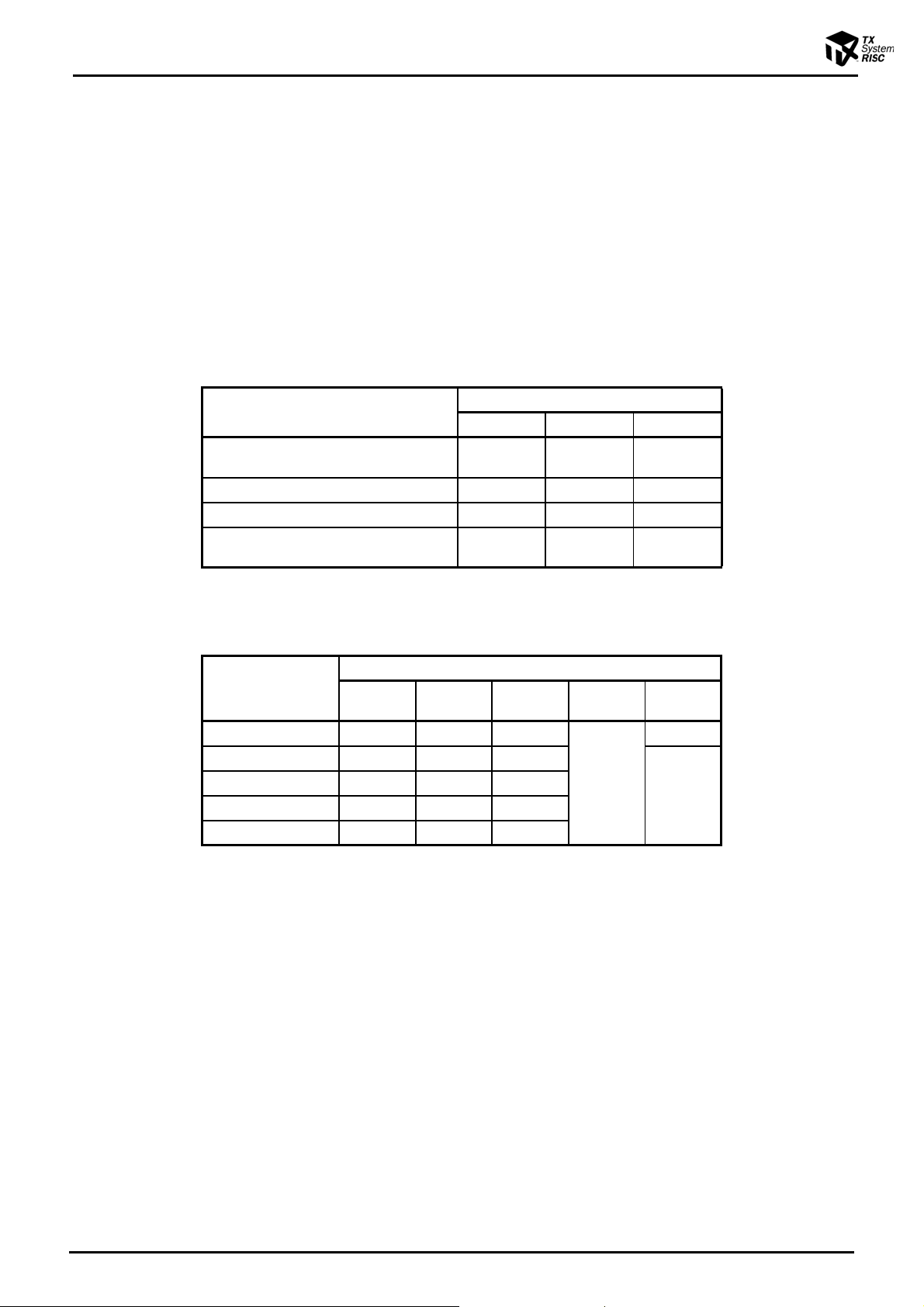
5. I/O Ports
5.1 Port P1 (P17 to P10)
5.1 Port P1 (P17 to P10)
Port P1 is an 8-bit input/output port which can be configured as an input or an output in one-bit unit. Input/output
mode is specified by the P1 control register (P1CR).
During reset, the P1DR, P1CR and P1LCR are initialized to “0”.
Port P1 is also used as UART input/output, an external interrupt input, serial interface input/output and segment
output of LCD. It is necessary to set registers for using each function. The following table shows register programming for multi function ports. When the port P16 is used, set not only P16 port registers but also P31 port register.
Also set not only port P17 registers but also P32 register similarly. Though the TMP86CH22UG do not have P31 and
P32 ports, it is necessary to set P3 port registers for keeping software compatibility with TMP86C923XB. For detail,
refer to Table 5-2 and Table 5-3 and then refer to description of P3OUTCR and P3DR registers.
TMP86CH22UG
Table 5-1 Register programming for P15 to P10
Function (Port P15 to P10)
Port input, UART input, SIO input or
external interrupt input
Port "0" output "0" "1" "0"
Port "1" output and UART output "1" "1" "0"
LCD segment output
Note: Asterisk (*) indicates "1" or "0" either of which can be selected.
P1DR[5:0] P1CR[5:0] P1LCR[5:0]
*"0""0"
*
Table 5-2 Register programming for P16
Programmed Value
Function (Port P16)
SIO output * "0" "0"
Port input * "0" "0"
Port "0" output "0" "1" "0"
Port "1" output "1" "1" "0"
LCD segment output * * "1"
P1DR[6] P1CR[6] P1LCR[6] P3DR[1]
Programmed Value
*"1"
P3OUTCR[1]
(SIOEN1)
"1"
"1"
"0"
Note 1: When P16 is used as port output, set in order each registers as follows. If it is not set appropriately, an overcurrent may
flow causing damage to the emulation chip (86C923XB).
STEP 1. P3OUTCR<SIOEN1> = “0”
STEP 2 P1LCR[6] = “0”
STEP 3. P1CR[6] = “1”
Note 2: When P16 is used as SO output, set in order each registers as follows. If it is not set appropriately, an overcurrent may
flow causing damage to the emulation chip (86C923XB).
STEP 1. P1LCR[6]="0"
STEP 2. P1CR[6]="0"
STEP 3. P3OUTCR<SIOEN1>="1"
Note 3: Asterisk (*) indicates "1" or "0" either of which can be selected.
Page 50
Page 62
TMP86CH22UG
Table 5-3 Register programming for P17
Programmed Value
Function (Port P17)
SIO output * "0" "0"
Port input or SIO input * "0" "0"
Port "0" output "0" "1" "0"
Port "1" output "1" "1" "0"
LCD segment output * * "1"
P1DR[7] P1CR[7] P1LCR[7] P3DR[2]
"1"
Note 1: When P17 is used as port output, set in order each registers as follows. If it is not set appropriately, an overcurrent may
flow causing damage to the emulation chip (86C923XB).
STEP 1. P3OUTCR<SIOEN2> = “0”
STEP 2 P1LCR[7] = “0”
STEP 3. P1CR[7] = “1”
Note 2: When P17 is used as SCK output, set in order each registers as follows. If it is not set appropriately, an overcurrent may
flow causing damage to the emulation chip (86C923XB).
P3OUTCR[2]
(SIOEN2)
"1"
"0"
STEP 1. P1LCR[7]="0"
STEP 2. P1CR[7]="0"
STEP 3. P3OUTCR<SIOEN2>="1"
Note 3: Asterisk (*) indicates "1" or "0" either of which can be selected.
Table 5-4 Values Read from P1DR and register programming
Conditions
P1CR P1LCR
"0" "0" Terminal input data
"0" "1" "0"
"1"
"0"
"1"
Values Read from P1DR
Output latch contents
Page 51
Page 63

5. I/O Ports
5.1 Port P1 (P17 to P10)
STOP
OUTEN
P1LCRi input
P1LCR[i]
P1CR[i] input
P1CR[i]
Data input (P1DR[i])
Data output (P1DR[i])
P3DR[1]
P3OUTCR<SIOEN1>
P3DR[1]
P3OUTCR<SIOEN1>
DQ
DQ
D
Q
Output latch
TMP86CH22UG
(In case of P16)
(In case of P17)
(Others)
P1i
P1DR
(0001H)
R/W
P1LCR
(0F9EH)
LCD data output
Note1 : i = 7 to 0
Note2 : STOP is bit7 in SYSCR1
Note3 : OUTEN is bit4 in SYSCR1
(P1DR[1])
TXD output
(P1DR[6])
SO output
P3OUTCR<SIOEN1>
(P1DR[7])
SCK output
P3OUTCR<SIOEN2>
0
Y
1
S
0
Y
1
S
Figure 5-2 Port 1
76543210
P17
SEG24
SCK
76543210
P1LCR
P16
SEG25
SO
P15
SEG26
SI
P14
SEG27
INT3
Port P1/segment output control
(set for each bit individually)
P13
SEG28
INT2
P12
SEG29
INT1
P11
SEG30
TXD
P10
SEG31
RXD
0: P1 input/output port or secondary function (expect for segment)
1: Segment output
(In case of P11)
(In case of P16)
(In case of P17)
(Others)
(Initial value: 0000 0000)
(Initial value: 0000 0000)
R/W
P1CR
(0009H)
76543210
(Initial value: 0000 0000)
P1CR
P1 port input/output control
(set for each bit individually)
0: Input mode, SO output or
1: Output mode
SCK output
Note 1: When P16 and P17 is used as port output or SIO output, set in order each registers according to notes of Table 5-2 and
Table 5-3.
Note 2: The port placed in input mode reads the pin input state. Therefore, when the input and output modes are used together,
the output latch (P1DR) contents for the port in input mode might be changed by executing a bit manipulation instruction.
Page 52
R/W
Page 64

TMP86CH22UG
5.2 Port P2 (P22 to P20)
Port P2 is a 3-bit input/output port.
It is also used as an external interrupt, a STOP mode release signal input, and low-frequency crystal oscillator connection pins. When used as an input port or a secondary function pins, respective output latch (P2DR) should be set
to “1”.
During reset, the output latch is initialized to “1”.
A low-frequency crystal oscillator (32.768 kHz) is connected to pins P21 (XTIN) and P22 (XTOUT) in the dualclock mode. In the single-clock mode, pins P21 and P22 can be used as normal input/output ports.
It is recommended that pin P20 should be used as an external interrupt input, a STOP mode release signal input, or
an input port. If it is used as an output port, the interrupt latch is set on the falling edge of the output pulse.
P2 port output latch (P2DR) and P2 port terminal input (P2PRD) are located on their respective address.
When read the output latch data, the P2DR register should be read and when read the terminal input data, the
P2PRD register should be read. If a read instruction is executed for port P2, read data of bits 7 to 3 are unstable.
Data input (P2PRD[0])
Data input
Data output (P2DR[0])
Second function input
Data input (P2PRD[1])
Data output (P2DR[1])
Data input (P2PRD[2])
Data output (P2DR[2])
P2DR
(0002H)
R/W
P2PRD
(0F9CH)
Read only
D Q
Output latch
Data input
D Q
Output latch
Data input
D Q
Output latch
STOP
OUTEN
XTEN
fs
Osc. enable
Note1 : STOP is bit7 in SYSCR1.
Note2 : OUTEN is bit4 in SYSCR1.
Figure 5-3 Port 2
76543210
P22
XTOUT
76543210
P22 P21 P20
P21
XTIN
P20
INT5
STOP
(Initial value: **** *111)
P20 (INT5, STOP)
P21 (XTIN)
P22 (XTOUT)
Note: Port P20 is used as STOP pin. Therefore, when stop mode is started, OUTEN does not affect to P20, and P20 becomes
High-Z mode.
Page 53
Page 65

5. I/O Ports
5.3 Port P3 (P37, P34 to P33)
5.3 Port P3 (P37, P34 to P33)
Port P3 is a 1-bit output and a 2-bit input/output port. It can be selected whether output circuit of P34 to P33 port is
C-MOS output or a sink open drain individually, by setting P3OUTCR. When a corresponding bit of P3OUTCR is
“0”, the output circuit is selected to a sink open drain and when a corresponding bit of P3OUTCR is “1”, the output
circuit is selected to a C-MOS output.
During reset, the P3DR is initialized to "1", and the P3OUTCR is initialized to "0".
Port P3 is also used as a timer/counter input/output, divider output. It is necessary to set registers for using each
function. The following table shows register programming for multi function ports.
P3 port output latch (P3DR) and P3 port terminal input (P3PRD) are located on their respective address. When
read the output latch data, the P3DR should be read and when read the terminal input data, the P3PRD register
should be read. If a read instruction is executed for each registers of P3 port, read data of reserved bits are unstable.
TMP86CH22UG
Table 5-5 Register programming for P34 to P33
Port input or timer counter input
Port "0" output "0"
Port "1" output or timer counter output "1"
Table 5-6 Register programming for P37
Port "0" output "0"
Port "1" output or divider output "1"
STOP
OUTEN
P3OUTCR[i]
P3OUTCR[i] input
Data input (P3PRD[i])
Output latch read (P3DR[i])
Function (Port P34 to P33)
Function (Port P37)
DQ
Programmed Value
P3DR[4:3] P3OUTCR[4:3]
"1" "0"
Programming
for each
applications
Programmed
Val ue
P3DR[7]
Data output (P3DR[i])
Second function output
Second function input
STOP
OUTEN
P3OUTCR[7]
Data output (P3DR[7])
Second function output
DQ
Output latch
a) P34, P33
DQ
Output latch
b) P37
Figure 5-4 Port 3
Page 54
P3i
Note1 : i = 4,3
Note2 : STOP is bit7 in SYSCR1.
Note3 : OUTEN is bit4 in SYSCR1.
P37
Page 66

76543210
P3DR
(0003H)
R/W
P37
DVO
P34
PWM5
PDO5
TC5
P33
PWM6
PDO6
PPG6
TC6
"1" "1" "1" (Initial value: 1**1 1***)
Note 1: Make sure to write "1" to bit2 to bit0 in P3DR.
Note 2: If a read instruction is executed for P3DR, read data of bits 6 to 5 and bit 2 to 0 are unstable.
TMP86CH22UG
P3OUTCR
(0004H)
76543210
P34 P33 SIOEN2 SIOEN1 "0" (Initial value: **** 0000)
P34, P33
SIOEN1 Port P16 control
Port P3 output circuit control
(set for each bit individually)
0: Sink open-drain output
1: C-MOS output
0: SCK input, Port input, Port output or LCD output
1: SCK output
0: Port input, Port output or LCD output
1: SO output
Note 1: When P16 and P17 is used as port output or SIO output, set in order each registers according to notes of Table 1-2 and
Table 1-3.
Note 2: If a read instruction is executed for P3OUTCR, read data of bits 7 to 5 and bit 0 are unstable.
Note 3: Make sure to write "0" to bit 0 in P3OUTCR.
P3PRD
(0F9DH)
Read only
76543210
P34 P33
Note 1: If a read instruction is executed for P3PRD, read data of bits 7 to 5 and bits 2 to 0 are unstable.
R/WSIOEN2 Port P17 control
Page 55
Page 67

5. I/O Ports
5.4 Port P5 (P57 to P50)
5.4 Port P5 (P57 to P50)
Port P5 is an 8-bit input/output port which can be configured as an input or an output in one-bit unit. Input/output
mode is spedified by the P5 control register (P5CR).
During reset, the P5DR, P5CR and P5LCR are initialized to “0”.
Port P5 is also used as a segment output of LCD. It is necessary to set registers for using each function. The fol-
lowing table shows register programming for multi function ports.
TMP86CH22UG
Table 5-7 Register programming for P57 to P50
Function (Port P57 to P50)
Port input * "0" "0"
Port "0" output "0" "1" "0"
Port "1" output and UART output "1" "1" "0"
LCD segment output * * "1"
P5DR[7:0] P5CR[7:0] P5LCR[7:0]
Note: Asterisk (*) indicates "1" or "0" either of which can be selected.
Table 5-8 Values Read from P5DR and register programming
STOP
OUTEN
Conditions
P5CR P5LCR
"0" "0" Terminal input data
"0" "1" "0"
"1"
"0"
"1"
Values Read from P5DR
Output latch contents
Programmed Value
P5LCR[i] input
P5LCR[i]
P5CR[i] input
P5CR[i]
Data input (P5DR[i])
Data output (P5DR[i])
LCD data output
DQ
DQ
DQ
Output latch
Figure 5-5 Port 5
P5i
Note1 : i = 7 to 0
Note2 : STOP is bit7 in SYSCR1
Note3 : OUTEN is bit4 in SYSCR1
Page 56
Page 68

TMP86CH22UG
P5DR
(0005H)
R/W
P5LCR
(0F9FH)
P5CR
(000AH)
76543210
P57
SEG16
76543210
P5LCR
76543210
P5CR
P56
SEG17
Port P5/segment output control
(set for each bit individually)
P5 port input/output control
(set for each bit individually)
P55
SEG18
P54
SEG19
P53
SEG20
0: P5 input/output port
1: LCD segment output
0: Input mode
1: Output mode
P52
SEG21
P51
SEG22
P50
SEG23
(Initial value: 0000 0000)
(Initial value: 0000 0000)
(Initial value: 0000 0000)
Note: The port placed in input mode reads the pin input state. Therefore, when the input and output modes are used together, the
output latch (P5DR) contents for the port in input mode might be changed by executing a bit manipulation instruction.
R/W
R/W
Page 57
Page 69

5. I/O Ports
5.5 Port P6 (P64 to P61)
5.5 Port P6 (P64 to P61)
Port P6 is an 4-bit input/output port which can be configured as an input or an output in one-bit unit. Input/output
mode is specified by the P6 control register (P6CR1) and input control register (P6CR2).
During reset, the output latch (P6DR) and P6CR1 are initialized to "0", P6CR2 is initialized to "1".
Port P6 is also used as an analog input, Key on Wake up input, timer/counter input and external interrupt input. It
is necessary to set registers for using each function. The following table shows register programming for multi function ports.
TMP86CH22UG
Table 5-9 Register programming for P64 to P61
Function (Port P64 to P61)
Port input, external interrupt input or timer counter
input
Analog input or Key on wake up input * "0" "0"
Port "0" output "0" "1" *
Port "1" output "1" "1" *
Note: Asterisk (*) indicates "1" or "0" either of which can be selected.
P6DR[4:1] P6CR1[4:1] P6CR2[4:1]
*"0""1"
Table 5-10 Values Read from P6DR and register programming
Conditions
P6CR1 P6CR2
"0" "0" "0"
"0" "1" Terminal input data
"1"
"0"
"1"
Values Read from P6DR
Output latch contents
Programmed Value
Page 58
Page 70

TMP86CH22UG
P6CR2[i]
P6CR2[i] input
P6CR1[i]
P6CR1[i] input
Second function input
Data input (P6DR[i])
Data output (P6DR[i])
STOP
OUTEN
Analog input
AINDS
SAIN
STOP2
Key-on wakeup
P6CR2[4]
P6CR2[4] input
P6CR1[4]
P6CR1[4] input
Data input (P6DR[4])
DQ
DQ
DQ
DQ
DQ
a) P63 to P61
P6i
Note1 : i = 3 to 1
Note2 : STOP is bit 7 in SYSCR1.
Note3 : SAIN is AD input select signal.
Note4 : STOP2EN is bit4 in STOPCR.
P6DR
(0006H)
R/W
P6CR1
(000BH)
Data output (P6DR[4])
DQ
P64
STOP
OUTEN
Analog input
AINDS
SAIN
b) P64
Figure 5-6 Port 6 and P6CR
76543210
P64
AIN4
STOP2
76543210
"0" "0" "0" "0" (Initial value: ***0 000*)
P6CR1
I/O control for port P6
(Specified for each bit)
P63
AIN3
INT0
0: Port input, Key on wake up input, Analog input, external input
or timer counter input
1: Port output
P62
AIN2
ECNT
P61
AIN1
ECIN
(Initial value: ***0 000*)
R/W
Note 1: Make sure to write "0" to bit7 to bit5, bit0 in P6CR1.
P6CR2
(000CH)
76543210
P6CR2
P6 port input control
(Specified for each bit)
(Initial value: ***1 111*)
0: Analog input or Key on wake up input
1: Port input, external interrupt input or timer counter input
Page 59
R/W
Page 71

5. I/O Ports
5.6 Port P7 (P76 to P70)
5.6 Port P7 (P76 to P70)
Port P7 is a 7-bit input/output port which can be configured as an input or an output in one-bit unit. Input/output
mode is spedified by the P7 control register (P7CR).
During reset, the P7DR, P7CR and P7LCR are initialized to “0”.
Port P7 is also used as a segment output of LCD. It is necessary to set registers for using each function. The fol-
lowing table shows register programming for multi function ports.
TMP86CH22UG
Table 5-11 Register programming for P76 to P70
Function (Port P76 to P70)
Port input * "0" "0"
Port "0" output "0" "1" "0"
Port "1" output and UART output "1" "1" "0"
LCD segment output * * "1"
P7DR[6:0] P7CR[6:0] P7LCR[6:0]
Note: Asterisk (*) indicates "1" or "0" either of which can be selected.
Table 5-12 Values Read from P7DR and register programming
STOP
OUTEN
Conditions
P7CR P7LCR
"0" "0" Terminal input data
"0" "1" "0"
"1"
"0"
"1"
Values Read from P7DR
Output latch contents
Programmed Value
P7LCR[i] input
P7LCR[i]
P7CR[i] input
P7CR[i]
Data input (P7DR[i])
Data output (P7DR[i])
LCD data output
DQ
DQ
DQ
Output latch
Figure 5-7 Port 7
P7i
Note1 : i = 6 to 0
Note2 : STOP is bit7 in SYSCR1.
Note3 : OUTEN is bit4 in SYSCR1.
Page 60
Page 72

TMP86CH22UG
P7DR
(0007H)
R/W
P7LCR
(0FA0H)
76543210
P76
SEG9
76543210
"0" (Initial value: 0000 0000)
P7LCR
Port P7/segment output control
(set for each bit individually)
P75
SEG10
P74
SEG11
P73
SEG12
0: P7 input/output port
1: LCD segment output
P72
SEG13
P71
SEG14
P70
SEG15
(Initial value: 0000 0000)
Note: Because the LCD driver does not operate correctly, always set "0" to bit7 of P7LCR.
P7CR
(000DH)
76543210
(Initial value: 0000 0000)
P7CR
P7 port input/output control
(set for each bit individually)
0: Input mode
1: Output mode
Note: The port placed in input mode reads the pin input state. Therefore, when the input and output modes are used together, the
output latch (P7DR) contents for the port in input mode might be changed by executing a bit manipulation instruction.
R/W
R/W
Page 61
Page 73

5. I/O Ports
5.6 Port P7 (P76 to P70)
TMP86CH22UG
Page 62
Page 74

6. Watchdog Timer (WDT)
The watchdog timer is a fail-safe system to detect rapidly the CPU malfunctions such as endless loops due to spu-
rious noises or the deadlock conditions, and return the CPU to a system recovery routine.
The watchdog timer signal for detecting malfunctions can be programmed only once as “reset request” or “inter-
rupt request”. Upon the reset release, this signal is initialized to “reset request”.
When the watchdog timer is not used to detect malfunctions, it can be used as the timer to provide a periodic inter-
rupt.
Note: Care must be taken in system design since the watchdog timer functions are not be operated completely due to
effect of disturbing noise.
6.1 Watchdog Timer Configuration
fc/223 or fs/2
fc/221 or fs/2
fc/219 or fs/2
fc/217 or fs/2
Internal reset
15
13
11
9
Selector
2
Binary counters
Clock
Clear
1 2
Overflow
WDT output
Reset release
R
S
Interrupt request
TMP86CH22UG
Q
Reset
request
INTWDT
interrupt
request
WDTT
Q
SR
WDTEN
0034
H
WDTCR1 WDTCR2
Watchdog timer control registers
Writing
disable code
Controller
0035
Writing
clear code
H
Figure 6-1 Watchdog Timer Configuration
WDTOUT
Page 63
Page 75

6. Watchdog Timer (WDT)
6.2 Watchdog Timer Control
6.2 Watchdog Timer Control
The watchdog timer is controlled by the watchdog timer control registers (WDTCR1 and WDTCR2). The watch-
dog timer is automatically enabled after the reset release.
6.2.1 Malfunction Detection Methods Using the Watchdog Timer
The CPU malfunction is detected, as shown below.
If the CPU malfunctions such as endless loops or the deadlock conditions occur for some reason, the watchdog timer output is activated by the binary-counter overflow unless the binary counters are cleared. When
WDTCR1<WDTOUT> is set to “1” at this time, the reset request is generated and then internal hardware is
initialized. When WDTCR1<WDTOUT> is set to “0”, a watchdog timer interrupt (INTWDT) is generated.
The watchdog timer temporarily stops counting in the STOP mode including the warm-up or IDLE/SLEEP
mode, and automatically restarts (continues counting) when the STOP/IDLE/SLEEP mode is inactivated.
TMP86CH22UG
1. Set the detection time, select the output, and clear the binary counter.
2. Clear the binary counter repeatedly within the specified detection time.
Note:The watchdog timer consists of an internal divider and a two-stage binary counter. When the clear code 4EH
is written, only the binary counter is cleared, but not the internal divider. The minimum binary-counter overflow
time, that depends on the timing at which the clear code (4EH) is written to the WDTCR2 register, may be 3/
4 of the time set in WDTCR1<WDTT>. Therefore, write the clear code using a cycle shorter than 3/4 of the
time set to WDTCR1<WDTT>.
Example :Setting the watchdog timer detection time to 221/fc [s], and resetting the CPU malfunction detection
LD (WDTCR2), 4EH : Clears the binary counters.
Within 3/4 of WDT
detection time
Within 3/4 of WDT
detection time
LD (WDTCR1), 00001101B
LD
:
:
LD (WDTCR2), 4EH : Clears the binary counters.
:
:
LD (WDTCR2), 4EH : Clears the binary counters.
(WDTCR2), 4EH : Clears the binary counters (always clears immediately before and
← 10, WDTOUT ← 1
: WDTT
after changing WDTT).
Page 64
Page 76

Watchdog Timer Control Register 1
TMP86CH22UG
WDTCR1
(0034H)
76543210
(ATAS) (ATOUT) WDTEN WDTT WDTOUT (Initial value: **11 1001)
WDTEN Watchdog timer enable/disable
WDTT
WDTOUT Watchdog timer output select
Watchdog timer detection time
[s]
0: Disable (Writing the disable code to WDTCR2 is required.)
1: Enable
NORMAL1/2 mode
DV7CK = 0 DV7CK = 1
00
01
10
11
0: Interrupt request
1: Reset request
25
/fc 217/fs 217/fs
2
23
2
/fc 215/fs 215fs
21
fc 213/fs 213fs
2
19
/fc 211/fs 211/fs
2
SLOW1/2
mode
Note 1: After clearing WDTOUT to “0”, the program cannot set it to “1”.
Note 2: fc: High-frequency clock [Hz], fs: Low-frequency clock [Hz], *: Don’t care
Note 3: WDTCR1 is a write-only register and must not be used with any of read-modify-write instructions. If WDTCR1 is read, a
don’t care is read.
Note 4: To activate the STOP mode, disable the watchdog timer or clear the counter immediately before entering the STOP mode.
After clearing the counter, clear the counter again immediately after the STOP mode is inactivated.
Note 5: To clear WDTEN, set the register in accordance with the procedures shown in “1.2.3 Watchdog Timer Disable”.
Watchdog Timer Control Register 2
Write
only
Write
only
Write
only
WDTCR2
(0035H)
76543210
WDTCR2
Write
Watchdog timer control code
Note 1: The disable code is valid only when WDTCR1<WDTEN> = 0.
Note 2: *: Don’t care
Note 3: The binary counter of the watchdog timer must not be cleared by the interrupt task.
Note 4: Write the clear code 4EH using a cycle shorter than 3/4 of the time set in WDTCR1<WDTT>.
6.2.2 Watchdog Timer Enable
Setting WDTCR1<WDTEN> to “1” enables the watchdog timer. Since WDTCR1<WDTEN> is initialized
to “1” during reset, the watchdog timer is enabled automatically after the reset release.
(Initial value: **** ****)
4EH: Clear the watchdog timer binary counter (Clear code)
B1H: Disable the watchdog timer (Disable code)
D2H: Enable assigning address trap area
Others: Invalid
Write
only
Page 65
Page 77

6. Watchdog Timer (WDT)
6.2 Watchdog Timer Control
6.2.3 Watchdog Timer Disable
To disable the watchdog timer, set the register in accordance with the following procedures. Setting the register in other procedures causes a malfunction of the microcontroller.
Note:While the watchdog timer is disabled, the binary counters of the watchdog timer are cleared.
Example :Disabling the watchdog timer
TMP86CH22UG
1. Set the interrupt master flag (IMF) to “0”.
2. Set WDTCR2 to the clear code (4EH).
3. Set WDTCR1<WDTEN> to “0”.
4. Set WDTCR2 to the disable code (B1H).
DI
LD (WDTCR2), 04EH : Clears the binary coutner
LDW (WDTCR1), 0B101H
: IMF
: WDTEN
Table 6-1 Watchdog Timer Detection Time (Example: fc = 16.0 MHz, fs = 32.768 kHz)
Watchdog Timer Detection Time[s]
WDTT
DV7CK = 0 DV7CK = 1
00 2.097 4 4
01 524.288 m 1 1
10 131.072 m 250 m 250 m
11 32.768 m 62.5 m 62.5 m
NORMAL1/2 mode
6.2.4 Watchdog Timer Interrupt (INTWDT)
When WDTCR1<WDTOUT> is cleared to “0”, a watchdog timer interrupt request (INTWDT) is generated
by the binary-counter overflow.
← 0
← 0, WDTCR2 ← Disable code
SLOW
mode
A watchdog timer interrupt is the non-maskable interrupt which can be accepted regardless of the interrupt
master flag (IMF).
When a watchdog timer interrupt is generated while the other interrupt including a watchdog timer interrupt
is already accepted, the new watchdog timer interrupt is processed immediately and the previous interrupt is
held pending. Therefore, if watchdog timer interrupts are generated continuously without execution of the
RETN instruction, too many levels of nesting may cause a malfunction of the microcontroller.
To generate a watchdog timer interrupt, set the stack pointer before setting WDTCR1<WDTOUT>.
Example :Setting watchdog timer interrupt
LD SP, 023FH : Sets the stack pointer
LD (WDTCR1), 00001000B
: WDTOUT
← 0
Page 66
Page 78

6.2.5 Watchdog Timer Reset
When a binary-counter overflow occurs while WDTCR1<WDTOUT> is set to “1”, a watchdog timer reset
request is generated. When a watchdog timer reset request is generated, the internal hardware is reset. The reset
time is maximum 24/fc [s] (1.5 µs @ fc = 16.0 MHz).
Note:When a watchdog timer reset is generated in the SLOW1 mode, the reset time is maximum 24/fc (high-fre-
quency clock) since the high-frequency clock oscillator is restarted. However, when crystals have inaccuracies upon start of the high-frequency clock oscillator, the reset time should be considered as an approximate
value because it has slight errors.
Clock
TMP86CH22UG
219/fc [s]
217/fc
(WDTT=11)
Binary counter
Overflow
INTWDT interrupt request
(WDTCR1<WDTOUT>= "0")
Internal reset
(WDTCR1<WDTOUT>= "1")
1
2
Write 4E
30 1 2 3 0
to WDTCR2
H
Figure 6-2 Watchdog Timer Interrupt
A reset occurs
Page 67
Page 79

6. Watchdog Timer (WDT)
6.3 Address Trap
6.3 Address Trap
The Watchdog Timer Control Register 1 and 2 share the addresses with the control registers to generate address
traps.
Watchdog Timer Control Register 1
TMP86CH22UG
WDTCR1
(0034H)
7654 3 21 0
ATAS ATOUT (WDTEN) (WDTT) (WDTOUT) (Initial value: **11 1001)
ATAS
ATOUT Select opertion at address trap
Select address trap generation in
the internal RAM area
0: Generate no address trap
1: Generate address traps (After setting ATAS to “1”, writing the control code
D2H to WDTCR2 is reguired)
0: Interrupt request
1: Reset request
Watchdog Timer Control Register 2
WDTCR2
(0035H)
76543210
WDTCR2
Write
Watchdog timer control code
and address trap area control
code
D2H: Enable address trap area selection (ATRAP control code)
4EH: Clear the watchdog timer binary counter (WDT clear code)
B1H: Disable the watchdog timer (WDT disable code)
Others: Invalid
6.3.1 Selection of Address Trap in Internal RAM (ATAS)
WDTCR1<ATAS> specifies whether or not to generate address traps in the internal RAM area. To execute
an instruction in the internal RAM area, clear WDTCR1<ATAS> to “0”. To enable the WDTCR1<ATAS> setting, set WDTCR1<ATAS> and then write D2H to WDTCR2.
Write
only
(Initial value: **** ****)
Write
only
Executing an instruction in the SFR or DBR area generates an address trap unconditionally regardless of the
setting in WDTCR1<ATAS>.
6.3.2 Selection of Operation at Address Trap (ATOUT)
When an address trap is generated, either the interrupt request or the reset request can be selected by
WDTCR1<ATOUT>.
6.3.3 Address Trap Interrupt (INTATRAP)
While WDTCR1<ATOUT> is “0”, if the CPU should start looping for some cause such as noise and an
attempt be made to fetch an instruction from the on-chip RAM (while WDTCR1<ATAS> is “1”), DBR or the
SFR area, address trap interrupt (INTATRAP) will be generated.
An address trap interrupt is a non-maskable interrupt which can be accepted regardless of the interrupt master flag (IMF).
When an address trap interrupt is generated while the other interrupt including a watchdog timer interrupt is
already accepted, the new address trap is processed immediately and the previous interrupt is held pending.
Therefore, if address trap interrupts are generated continuously without execution of the RETN instruction, too
many levels of nesting may cause a malfunction of the microcontroller.
To generate address trap interrupts, set the stack pointer beforehand.
Page 68
Page 80

6.3.4 Address Trap Reset
While WDTCR1<ATOUT> is “1”, if the CPU should start looping for some cause such as noise and an
attempt be made to fetch an instruction from the on-chip RAM (while WDTCR1<ATAS> is “1”), DBR or the
SFR area, address trap reset will be generated.
When an address trap reset request is generated, the internal hardware is reset. The reset time is maximum
24/fc [s] (1.5 µs @ fc = 16.0 MHz).
Note:When an address trap reset is generated in the SLOW1 mode, the reset time is maximum 24/fc (high-fre-
quency clock) since the high-frequency clock oscillator is restarted. However, when crystals have inaccuracies upon start of the high-frequency clock oscillator, the reset time should be considered as an approximate
value because it has slight errors.
TMP86CH22UG
Page 69
Page 81

6. Watchdog Timer (WDT)
6.3 Address Trap
TMP86CH22UG
Page 70
Page 82

7. Time Base Timer (TBT)
The time base timer generates time base for key scanning, dynamic displaying, etc. It also provides a time base
timer interrupt (INTTBT).
7.1 Time Base Timer
7.1.1 Configuration
TMP86CH22UG
fc/223 or fs/2
fc/221 or fs/2
fc/216 or fs/2
fc/214 or fs/2
fc/213 or fs/2
fc/212 or fs/2
fc/211 or fs/2
fc/29 or fs/2
15
13
8
6
5
4
3
3
Time base timer control register
Figure 7-1 Time Base Timer configuration
7.1.2 Control
Time Base Timer is controled by Time Base Timer control register (TBTCR).
Time Base Timer Control Register
7 6543210
MPX
TBTCR
(0036H)
(DVOEN) (DVOCK) (DV7CK) TBTEN TBTCK (Initial Value: 0000 0000)
Source clock
TBTCR
Falling edge
TBTENTBTCK
detector
IDLE0, SLEEP0
release request
INTTBT
interrupt request
TBTEN
TBTCK
Time Base Timer
enable / disable
Time Base Timer interrupt
Frequency select : [Hz]
0: Disable
1: Enable
000
001
010
011
100
101
110
111
NORMAL1/2, IDLE1/2 Mode SLOW1/2
DV7CK = 0 DV7CK = 1
23
fc/2
21
fc/2
16
fc/2
14
fc/2
13
fc/2
12
fc/2
11
fc/2
9
fc/2
Note 1: fc; High-frequency clock [Hz], fs; Low-frequency clock [Hz], *; Don't care
Page 71
SLEEP1/2
15
fs/2
13
fs/2
8
fs/2
6
fs/2
5
fs/2
4
fs/2
3
fs/2
fs/2 –
Mode
fs/2
fs/2
–
–
–
–
–
15
13
R/W
Page 83

7. Time Base Timer (TBT)
7.1 Time Base Timer
Note 2: The interrupt frequency (TBTCK) must be selected with the time base timer disabled (TBTEN="0"). (The interrupt fre-
Example :Set the time base timer frequency to fc/216 [Hz] and enable an INTTBT interrupt.
Table 7-1 Time Base Timer Interrupt Frequency ( Example : fc = 16.0 MHz, fs = 32.768 kHz )
TMP86CH22UG
quency must not be changed with the disable from the enable state.) Both frequency selection and enabling can be performed simultaneously.
LD (TBTCR) , 00000010B ; TBTCK ← 010
LD (TBTCR) , 00001010B ; TBTEN ← 1
DI ; IMF ← 0
SET (EIRL) . 6
TBTCK
000 1.91 1 1
001 7.63 4 4
010 244.14 128 –
011 976.56 512 –
100 1953.13 1024 –
101 3906.25 2048 –
110 7812.5 4096 –
111 31250 16384 –
7.1.3 Function
An INTTBT ( Time Base Timer Interrupt ) is generated on the first falling edge of source clock ( The divider
output of the timing generato which is selected by TBTCK. ) after time base timer has been enabled.
The divider is not cleared by the program; therefore, only the first interrupt may be generated ahead of the set
interrupt period ( Figure 7-2 ).
Time Base Timer Interrupt Frequency [Hz]
NORMAL1/2, IDLE1/2 Mode NORMAL1/2, IDLE1/2 Mode SLOW1/2, SLEEP1/2 Mode
DV7CK = 0 DV7CK = 1
Source clock
TBTCR<TBTEN>
INTTBT
Figure 7-2 Time Base Timer Interrupt
Interrupt period
Enable TBT
Page 72
Page 84

7.2 Divider Output (DVO)
Approximately 50% duty pulse can be output using the divider output circuit, which is useful for piezoelectric
buzzer drive. Divider output is from
7.2.1 Configuration
Output latch
Data output
fc/213 or fs/2
fc/212 or fs/2
fc/211 or fs/2
fc/210 or fs/2
D Q
MPX
5
A
4
B
C Y
3
D
2
S
2
DVOCK
DVOEN
TBTCR
Divider output control register
(a) configuration (b) Timing chart
TMP86CH22UG
DVO pin.
DVO pin
Port output latch
TBTCR<DVOEN>
DVO pin output
7.2.2 Control
The Divider Output is controlled by the Time Base Timer Control Register.
Time Base Timer Control Register
7654321 0
TBTCR
(0036H)
DVOEN DVOCK (DV7CK) (TBTEN) (TBTCK) (Initial value: 0000 0000)
DVOEN
DVOCK
Divider output
enable / disable
Divider Output (
frequency selection: [Hz]
Figure 7-3 Divider Output
0: Disable
1: Enable
NORMAL1/2, IDLE1/2 Mode
DV7CK = 0 DV7CK = 1
DVO)
00
01
10
11
fc/2
fc/2
fc/2
fc/2
13
12
11
10
fs/2
fs/2
fs/2
fs/2
R/W
SLOW1/2
SLEEP1/2
Mode
5
4
3
2
fs/2
fs/2
fs/2
fs/2
5
4
3
2
R/W
Note: Selection of divider output frequency (DVOCK) must be made while divider output is disabled (DVOEN="0"). Also, in other
words, when changing the state of the divider output frequency from enabled (DVOEN="1") to disable(DVOEN="0"), do not
change the setting of the divider output frequency.
Page 73
Page 85

7. Time Base Timer (TBT)
7.2 Divider Output (DVO)
Example :1.95 kHz pulse output (fc = 16.0 MHz)
TMP86CH22UG
LD (TBTCR) , 00000000B ; DVOCK ← "00"
LD (TBTCR) , 10000000B ; DVOEN ← "1"
Table 7-2 Divider Output Frequency ( Example : fc = 16.0 MHz, fs = 32.768 kHz )
Divider Output Frequency [Hz]
DVOCK
00 1.953 k 1.024 k 1.024 k
01 3.906 k 2.048 k 2.048 k
10 7.813 k 4.096 k 4.096 k
11 15.625 k 8.192 k 8.192 k
NORMAL1/2, IDLE1/2 Mode
DV7CK = 0 DV7CK = 1
SLOW1/2, SLEEP1/2
Mode
Page 74
Page 86

8. 18-Bit Timer/Counter (TC1)
8.1 Configuration
INTTC1
F/F
11
TC1SR
CMP
TMP86CH22UG
H
TREG1A
M
TREG1B
A
B Y
4
5
or fs/2
or fs/2
12
13
fc/2
fc/2
2
SGEDG
TC1M
generator
Window pulse
2
S
C
6
or fs/2
14
fc/2
1
1
WGPSCK
TC6OUT
Edge detector
S
C
B Y
A
Pin
P33
ECNT Pin
CLEAR signal
18- bit up-counter
Y
10
Pulse width
measurement mode
Frequency
measurement mode
H
1
SEG
Edge detector
ECIN Pin
S
11
00
Timer/Event count modes
Y
CDEFGBA
3
11
23
13
fc/27fc/2
or fc/2
or fc/2
or fc/2
3
5
15
fs/2
fs/2
fs/2
TREG1A
L
TREG1A
fs
fc
22 1 12121
3
SGP
SEG
TC1C
TC1S
TC1M
TC6OUT
WGPSCK
SGEDG
TC1CR2
TC1CK
TC1CR1
PWM6/PDO6/PPG6
Figure 8-1 Timer/Counter1
Page 75
Page 87

8. 18-Bit Timer/Counter (TC1)
8.2 Control
8.2 Control
The Timer/counter 1 is controlled by timer/counter 1 control registers (TC1CR1/TC1CR2), an 18-bit timer register
(TREG1A), and an 8-bit internal window gate pulse setting register (TREG1B).
Timer register
TREG1AH
(0012H)
R/W
TREG1AM
(0011H)
R/W
TMP86CH22UG
76543210
−−−−−− TREG1AH (Initial value: ∗∗∗∗ ∗∗00)
76543210
TREG1AM (Initial value: 0000 0000)
TREG1AL
(0010H)
R/W
TREG1B
(0013H)
Ta
Tb
76543210
TREG1AL (Initial value: 0000 0000)
76543210
Ta Tb (Initial value: 0000 0000)
NORMAL1/2,IDLE1/2 modes
Setting "H" level period of the window
gate pulse
Setting "L" level period of the window
gate pulse
WGPSCK
00
01
10
00
01
10
DV7CK=0 DV7CK=1
(16 - Ta) × 2
(16 - Ta) × 2
(16 - Ta) × 2
(16 - Tb) × 2
(16 - Tb) × 2
(16 - Tb) × 2
12
13
14
12
13
14
/fc
/fc
/fc
/fc
/fc
/fc
(16 - Ta) × 2
(16 - Ta) × 2
(16 - Ta) × 2
(16 - Tb) × 2
(16 - Tb) × 2
(16 - Tb) × 2
4
/fs
5
/fs
6
/fs
4
/fs
5
/fs
6
/fs
SLOW1/2,
SLEEP1/2 modes
(16 - Ta) × 2
(16 - Ta) × 2
(16 - Ta) × 2
(16 - Tb) × 2
(16 - Tb) × 2
(16 - Tb) × 2
4
/fs
5
/fs
6
/fs
4
/fs
5
/fs
6
/fs
R/W
Page 76
Page 88

Timer/counter 1 control register 1
7 6543210
TC1CR1
(0014H)
TC1C TC1S TC1CK TC1M (Initial value: 1000 1000)
TMP86CH22UG
TC1C
TC1S TC1 start control
TC1CK TC1 source clock select
TC1M TC1 mode select
Counter/overfow flag
controll
0:
Clear Counter/overflow flag ( “1” is automatically set after clearing.)
1:
Not clear Counter/overflow flag
00:
Stop and counter clear and overflow flag clear
10:
Star t
*1:
Reserved
NORMAL1/2,IDLE1/2 modes
DV7CK="0" DV7CK="1"
fs/2
fs/2
fs/2
fc/2
fc/2
fc
fs
15
5
3
7
3
000:
001:
010:
011:
100:
101:
110:
111: External clock (ECIN pin input)
00:
01:
10:
11:
fc
fs
23
fc/2
13
fc/2
11
fc/2
7
fc/2
3
fc/2
Timer/Event counter mode
Reserved
Pulse width measurement mode
Frequency measurement mode
SLOW1/2
mode
fc
-
15
fs/2
5
fs/2
3
fs/2
-
-
SLEEP1/2
mode
fc
-
15
fs/2
5
fs/2
3
fs/2
-
-
R/W
R/W
R/W
R/W
Note 1: fc; High-frequency clock [Hz] fs; Low-frequency clock [Hz] * ; Don’t care
Note 2: Writing to the low-byte of the timer register 1A (TREG1AL, TREG1AM), the compare function is inhibited until the high-
byte (TREG1AH) is written.
Note 3: Set the mode and source clock, and edge (selection) when the TC1 stops (TC1S=00).
Note 4: “fc” can be selected as the source clock only in the timer mode during SLOW mode and in the pulse width measurement
mode during NORMAL 1/2 or IDLE 1/2 mode.
Note 5: When a read instruction is executed to the timer register (TREG1A), the counter immediate value, not the register set
value, is read out. Therefore it is impossible to read out the written value of TREG1A. To read the counter value, the read
instruction should be executed when the counter stops to avoid reading unstable value.
Note 6: Set the timer register (TREG1A) to
≥1.
Note 7: When using the timer mode and pulse width measurement mode, set TC1CK (TC1 source clock select) to internal clock.
Note 8: When using the event counter mode, set TC1CK (TC1 source clock select) to external clock.
Note 9: Because the read value is different from the written value, do not use read-modify-write instructions to TREG1A.
7
Note 10:fc/2
, fc/23can not be used as source clock in SLOW/SLEEP mode.
Note 11:The read data of bits 7 to 2 in TREG1AH are always “0”. (Data “1” can not be written.)
Page 77
Page 89

8. 18-Bit Timer/Counter (TC1)
8.2 Control
Timer/Counter 1 control register 2
76543210
TC1CR2
(0015H)
SEG SGP SGEDG WGPSCK TC6OUT "0" (Initial value: 0000 000*)
TMP86CH22UG
SEG
External input clock (ECIN) edge
select
SGP Window gate pulse select
SGEDG
WGPSCK
TC6OUT
Window gate pulse interrupt edge
select
Window gate pulse source clock
select
TC6 output (
PWM6/PDO6/PPG6)
external output select
0:1:Counts at the falling edge
Counts at the both (falling/rising) edges
00:
ECNT input
01:
Internal window gate pulse (TREG1B)
PWM6/PDO6/PPG6 (TC6)output
10:
Reserved
11:
0:1:Interrupts at the falling edge
Interrupts at the falling/rising edges
NORMAL1/2,IDLE1/2 modes
DV7CK="0" DV7CK="1"
00:
01:
10:
11:
12
2
/fc
13
/fc
2
14
/fc
2
Reserved
4
2
/fs
5
/fs
2
6
/fs
2
Reserved
0:1:Output to P33
No output to P33
SLOW1/2
mode
4
2
/fs
5
/fs
2
6
/fs
2
Reserved
Note 1: fc; High-frequency clock [Hz] fs; Low-frequency clock [Hz] *; Don't care
Note 2: Set the mode, source clock, and edge (selection) when the TC1 stops (TC1S = 00).
Note 3: If there is no need to use
PWM6/PDO6/PPG6 as window gate pulse of TC1 always write "0" to TC6OUT.
Note 4: Make sure to write TC1CR2 "0" to bit 0 in TC1CR2.
Note 5: When using the event counter mode or pulse width measurement mode, set SEG to "0".
SLEEP1/2
mode
4
2
/fs
5
/fs
2
6
/fs
2
Reserved
R/W
R/W
R/W
R/W
Page 78
Page 90

TC1 status register
7 6 543210
TC1SR
(0016H)
HECF HEOVF "0" "0" "0" "0" "0" "0" (Initial value: 0000 0000)
TMP86CH22UG
HECF Operating Status monitor
HEOVF Counter overflow monitor
8.3 Function
TC1 has four operating modes. The timer mode of the TC1 is used at warm-up when switching form SLOW mode
to NORMAL2 mode.
8.3.1 Timer mode
In this mode, counting up is performed using the internal clock. The contents of TREGIA are compared with
the contents of up-counter. If a match is found, an INTTC1 interrupt is generated, and the counter is cleared.
Counting up resumes after the counter is cleared.
Table 8-1 Source clock (internal clock) of Timer/Counter 1
NORMAL1/2, IDLE1/2 Mode
DV7CK = 0 DV7CK = 1
23
[Hz] fs/215 [Hz] fs/215 [Hz] fs/215 [Hz]
fc/2
13
fc/2
11
fc/2
7
fc/2
3
fc/2
fc fc fc (Note) - 62.5 ns - 16.4 ms -
fs fs - - - 30.5 ms - 8 s
0:1:Stop (during Tb) or disable
Under counting (during Ta)
0:1:No overflow
Overflow status
Source Clock Resolution Maximum Time Setting
fs =32.768
kHz
fc = 16 MHz
fs/2
fs/2
fc/2
fc/2
SLOW Mode SLEEP Mode fc = 16 MHz
5
3
7
3
5
fs/2
3
fs/2
--8 ms-2.1 s-
- - 0.5 ms - 131.1 ms -
fs/2
fs/2
5
3
0.52 s 1 s 38.2 h 72.8 h
512 ms 0.98 ms 2.2 min 4.3 min
128 ms 244 ms 0.6 min 1.07 min
Read
only
fs =32.768
kHz
Note: When fc is selected for the source clock in SLOW mode, the lower bits 11 of TREG1A is invalid, and a match of the upper
bits 7 makes interrupts.
Page 79
Page 91

8. 18-Bit Timer/Counter (TC1)
8.3 Function
Internal clock
TMP86CH22UG
Command Start
Up counter
TREG1A
INTTC1 interrupt
10 2 3 4 n
n
Figure 8-2 Timing chart for timer mode
8.3.2 Event Counter mode
It is a mode to count up at the falling edge of the ECIN pin input. When using this mode, set
TC1CR1<TC1CK> to the external clock and then set TC1CR2<SEG> to “0” (Both edges can not be used).
The countents of TREG1A are compared with the contents of up-counter. If a match is found, an INTTC1
interrupt is generated, and the counter is cleared. Counting up resumes for ECIN pin input edge each after the
counter is cleared.
The maximum applied frequency is fc/2
or SLEEP mode . Two or more machine cycles are required for both the “H” and “L” levels of the pulse width.
Start
1n-1 2 3 4 5 6
0
Match detect
4
[Hz] in NORMAL 1/2 or IDLE 1/2 mode and fs/24[Hz] in SLOW
Counter clear
ECIN pin input
Up counter
TREG1A
INTTC1 interrupt
10 2 2n-1 n 0 1
n
Match Detect
Figure 8-3 Event counter mode timing chart
Counter clear
Page 80
Page 92

8.3.3 Pulse Width Measurement mode
In this mode, pulse widths are counted on the falling edge of logical AND-ed pulse between ECIN pin input
(window pulse) and the internal clock. When using this mode, set TC1CR1<TC1CK> to suitable internal clock
and then set TC1CR2<SEG> to “0” (Both edges can not be used).
An INTTC1 interrupt is generated when the ECIN input detects the falling edge of the window pulse or both
rising and falling edges of the window pulse, that can be selected by TC1CR2<SGEDG>.
The contents of TREG1A should be read while the count is stopped (ECIN pin is low), then clear the counter
using TC1CR1<TC1C> (Normally, execute these process in the interrupt program).
When the counter is not cleared by TC1CR1<TC1C>, counting-up resumes from previous stopping value.
When up counter is counted up from 3FFFFH to 00000H, an overflow occurs. At that time, TC1SR<HEOVF>
is set to “1”. TC1SR<HEOVF> remains the previous data until the counter is required to be cleared by
TC1CR1<TC1C>.
Note:In pulse width measurement mode, if TC1CR1<TC1S> is written to "00" while ECIN input is "1", INTTC1 inter-
rupt occurs. According to the following step, when timer counter is stopped, INTTC1 interrupt latch should be
cleared to "0".
TMP86CH22UG
Example :
ECIN pin input
TC1STOP :
¦ ¦
DI ; Clear IMF
CLR (EIRL). 7 ; Clear bit7 of EIRL
LD (TC1CR1), 00011010B ; Stop timer couter 1
LD (I L L), 0 1111111B ; C lea r bit 7 of IL L
SET (EIRL). 7 ; Set bit7 of EIRL
EI ; Set IMF
¦ ¦
Note 1: When SGEDG (window gate pulse interrupt edge select) is set to both edges and ECIN pin input is "1" in
the pulse width measurement mode, an INTTC1 interrupt is generated by setting TC1S (TC1 start control)
to "10" (start).
Note 2: In the pulse width measurement mode, HECF (operating status monitor) cannot used.
Note 3: Because the up counter is counted on the falling edge of logical AND-ed pulse (between ECIN pin input and
the internal clock), if ECIN input becomes falling edge while internal source clock is "H" level, the up
counter stops plus "1".
Count StartCount Start Count Stop
Internal clock
AND-ed pulse
(Internal signal)
Up counter
INTTC1 interrupt
TC1CR1<TC1C>
10 2 3 n-2 n-1 n n+1 0 12
Read Clear
Interrupt
Figure 8-4 Pulse width measurement mode timing chart
Page 81
Page 93

8. 18-Bit Timer/Counter (TC1)
8.3 Function
8.3.4 Frequency Measurement mode
In this mode, the frequency of ECIN pin input pulse is measured. When using this mode, set
TC1CR1<TC1CK> to the external clock.
The edge of the ECIN input pulse is counted during “H” level of the window gate pulse selected by
TC1CR2<SGP>. To use ECNT input as a window gate pulse, TC1CR2<SGP> should be set to “00”.
An INTTC1 interrupt is generated on the falling edge or both the rising/falling edges of the window gate
pulse, that can be selected by TC1CR2<SGEDG>. In the interrupt service program, read the contents of
TREG1A while the count is stopped (window gate pulse is low), then clear the counter using
TC1CR1<TC1C>. When the counter is not cleared, counting up resumes from previous stopping value.
The window pulse status can be monitored by TC1SR<HECF>.
When up counter is counted up from 3FFFFH to 00000H, an overflow occurs. At that time,
TC1SR<HEOVF> is set to “1”. TC1SR<HEOVF> remains the previous data until the counter is required to be
cleared by TC1CR1<TC1C>.
TMP86CH22UG
Using TC6 output (
PWM6/PDO6/PPG6) for the window gate pulse, external output of PWM6/PDO6/PPG6 to
P33 can be controlled using TC1CR2<TC6OUT>. Zero-clearing TC1CR2<TC6OUT> outputs PWM6/
PDO6/PPG6 to P33; setting 1 in TC1CR2<TC6OUT> does not output PWM6/PDO6/PPG6 to P33.
(TC1CR2<
operate/stop
When the internal window gate pulse is selected, the window gate pulse is set as follows.
Table 8-2 Internal window gate pulse setting time
Ta
Tb
The internal window gate pulse consists of “H” level period (Ta) that is counting time and “L” level period
(Tb) that is counting stop time. Ta or Tb can be individually set by TREG1B. One cycle contains Ta + Tb.
TC6OUT> is used to control output to P33 only. Thus, use the timer counter 6 control register to
PWM6/PDO6/PPG6.)
Setting "H" level period of the window
gate pulse
Setting "L" level period of the window
gate pulse
WGPSCK
00
01
10
00
01
10
NORMAL1/2,IDLE1/2 modes
DV7CK=0 DV7CK=1
(16 - Ta) × 2
(16 - Ta) × 2
(16 - Ta) × 2
(16 - Tb) × 2
(16 - Tb) × 2
(16 - Tb) × 2
12
13
14
12
13
14
/fc
/fc
/fc
/fc
/fc
/fc
(16 - Ta) × 2
(16 - Ta) × 2
(16 - Ta) × 2
(16 - Tb) × 2
(16 - Tb) × 2
(16 - Tb) × 2
4
/fs
5
/fs
6
/fs
4
/fs
5
/fs
6
/fs
SLOW1/2,
SLEEP1/2 modes
(16 - Ta) × 2
(16 - Ta) × 2
(16 - Ta) × 2
(16 - Tb) × 2
(16 - Tb) × 2
(16 - Tb) × 2
4
/fs
5
/fs
6
/fs
4
/fs
5
/fs
6
/fs
R/W
Note 1: Because the internal window gate pulse is generated in synchronization with the internal divider, it may be
delayed for a maximum of one cycle of the source clock (WGPSCK) immediately after start of the timer.
Note 2: Set the internal window gate pulse when the timer counter is not operating or during the Tb period. When
Tb is overwritten during the Tb period, the update is valid from the next Tb period.
Note 3: In case of TC1CR2<SEG> = "1", if window gate pulse becomes falling edge, the up counter stops plus "1"
regardless of ECIN input level. Therefore, if ECIN is always "H" or "L" level, count value becomes "1".
Note 4: In case of TC1CR2<SEG> = "0", because the up counter is counted on the falling edge of logical AND-ed
pulse (between ECIN pin input and window gate pulse), if window gate pulse becomes falling edge while
ECIN input is "H" level, the up counter stops plus "1". Therefore, if ECIN input is always "H" level, count
value becomes "1".
Page 82
Page 94

Table 8-3 Table Setting Ta and Tb (WGPSCK = 10, fc = 16 MHz)
Setting Value Setting time Setting Value Setting time
0 16.38ms 8 8.19ms
1 15.36ms 9 7.17ms
2 14.34ms A 6.14ms
3 13.31ms B 5.12ms
4 12.29ms C 4.10ms
5 11.26ms D 3.07ms
6 10.24ms E 2.05ms
7 9.22ms F 1.02ms
Table 8-4 Table Setting Ta and Tb (WGPSCK = 10, fs = 32.768 kHz)
Setting Valuen Setting time Setting Value Setting time
0 31.25ms 8 15.63ms
1 29.30ms 9 13.67ms
2 27.34ms A 11.72ms
3 25.39ms B 9.77ms
4 23.44ms C 7.81ms
5 21.48ms D 5.86ms
6 19.53ms E 3.91ms
7 17.58ms F 1.95ms
TMP86CH22UG
Page 83
Page 95

8. 18-Bit Timer/Counter (TC1)
8.3 Function
ECIN pin input
Window gate
pulse
AND-ed pulse
(Internal signal)
TMP86CH22UG
Ta
Tb
Ta
Up counter
INTTC1 interrupt
TC1CR1<TC1C>
TC1CR2<SEG>
ECIN pin input
Window gate
pulse
Up counter
INTTC1 interrupt
TC1CR1<TC1C>
10 2 3 54 1 2 3 5646 0
Read
Clear
a) TC1CR2<SEG> = "0"
Ta
0
2 3 4 5 6 7 8 9 10
1
12 11
a) TC1CR2<SEG> = "1"
13
Read
Tb
0 12
Clear
2 3 4 5 6 7 8 9 1011
1
Ta
Figure 8-5 Timing chart for the frequency measurement mode (Window gate pulse falling
interrupt)
Page 84
Page 96

9. 8-Bit TimerCounter (TC5, TC6)
9.1 Configuration
Overflow
fc/2
fc/2
fc/2
fc/2
3
7
5
3
fs
fc
A
B Y
C
D
E
F
G
H
TC6CR
S
TC6CK
A Y
B
S
16-bit mode
TTREG6
8-bit up-counter
PWREG6
16-bit
mode
Clear
16-bit
mode
fc/211 or fs/2
TC6 pin
TC6M
TC6S
TFF6
PWM mode
TC6S
PDO, PPG mode
A
Y
B
S
Timer, Event
Counter mode
S
A
Y
B
PWM, PPG mode
Decode
TFF6
Timer F/F6
EN
TMP86CH22UG
INTTC6
interrupt request
Toggle
Q
Set
Clear
PDO, PWM,
PPG mode
PDO
PPG
6/PWM6/
6 pin
fc/211 or fs/2
fc/2
fc/2
fc/2
fc/2
TC5 pin
TC5M
TC5S
TFF5
fs
fc
3
7
5
3
A
B Y
C
D
E
F
G
H
TC5CR
S
TC5CK
Clear
TTREG5
8-bit up-counter
PWREG5
TC5S
Overflow
PWM mode
PDO mode
Timer,
Event Couter mode
PWM mode
Figure 9-1 8-Bit TimerCouter 5, 6
16-bit mode
16-bit mode
Decode
TFF5
Set
Clear
Timer F/F5
EN
INTTC5
interrupt request
Toggle
Q
PDO5/PWM5/
pin
PDO, PWM mode
16-bit mode
Page 85
Page 97

9. 8-Bit TimerCounter (TC5, TC6)
9.1 Configuration
9.2 TimerCounter Control
The TimerCounter 5 is controlled by the TimerCounter 5 control register (TC5CR) and two 8-bit timer registers
(TTREG5, PWREG5).
TimerCounter 5 Timer Register
TMP86CH22UG
TTREG5
(001EH)
R/W
PWREG5
(002AH)
R/W
76543210
(I n iti a l va l ue: 1111 1111 )
76543210
(I n iti a l va l ue: 1111 1111 )
Note 1: Do not change the timer register (TTREG5) setting while the timer is running.
Note 2: Do not change the timer register (PWREG5) setting in the operating mode except the 8-bit and 16-bit PWM modes while
the timer is running.
TimerCounter 5 Control Register
TC5CR
(001AH)
TFF5 Time F/F5 control
TC5CK Operating clock selection [Hz]
TC5S TC5 start control
TC5M TC5M operating mode select
76543210
TFF5 TC5CK TC5S TC5M (Initial value: 0000 0000)
0:1:Clear
Set
NORMAL1/2, IDLE1/2 mode SLOW1/2
DV7CK = 0 DV7CK = 1
000
001
010
011
100 fs fs fs
101 fc/2 fc/2 –
110 fc fc fc (Note 8)
111 TC5 pin input
0:1:Operation stop and counter clear
Operation start
000:
8-bit timer/event counter mode
001:
8-bit programmable divider output (PDO) mode
010:
8-bit pulse width modulation (PWM) output mode
16-bit mode
011:
(Each mode is selectable with TC6M.)
Reserved
1**:
fc/2
fc/2
fc/2
fc/2
11
7
5
3
fs/2
fc/2
fc/2
fc/2
3
7
5
3
SLEEP1/2
mode
3
fs/2
–
–
–
R/W
R/W
R/W
R/W
Note 1: fc: High-frequency clock [Hz] fs: Low-frequency clock[Hz]
Note 2: Do not change the TC5M, TC5CK and TFF5 settings while the timer is running.
Note 3: To stop the timer operation (TC5S= 1 → 0), do not change the TC5M, TC5CK and TFF5 settings. To start the timer opera-
tion (TC5S= 0 → 1), TC5M, TC5CK and TFF5 can be programmed.
Note 4: To use the TimerCounter in the 16-bit mode, set the operating mode by programming TC6CR<TC6M>, where TC5M must
be fixed to 011.
Note 5: To use the TimerCounter in the 16-bit mode, select the source clock by programming TC5CK. Set the timer start control
and timer F/F control by programming TC6CR<TC6S> and TC6CR<TFF6>, respectively.
Note 6: The operating clock settings are limited depending on the timer operating mode. For the detailed descriptions, see Table
9-1 and Table 9-2.
Page 86
Page 98

TMP86CH22UG
Note 7: The timer register settings are limited depending on the timer operating mode. For the detailed descriptions, see Table 9-
3.
Note 8: The operating clock fc in the SLOW or SLEEP mode can be used only as the high-frequency warm-up mode.
Page 87
Page 99
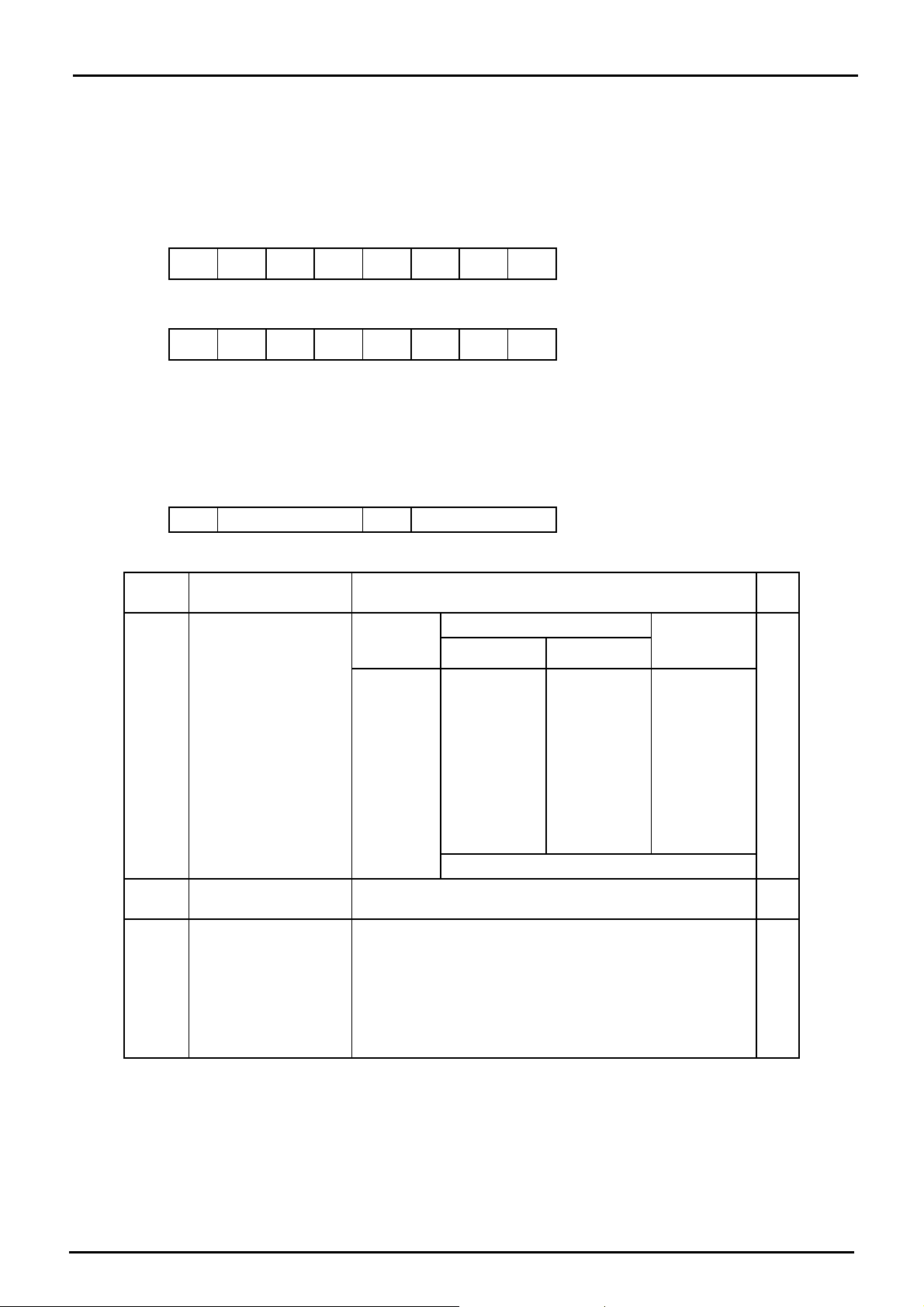
9. 8-Bit TimerCounter (TC5, TC6)
9.1 Configuration
The TimerCounter 6 is controlled by the TimerCounter 6 control register (TC6CR) and two 8-bit timer registers
(TTREG6 and PWREG6).
TimerCounter 6 Timer Register
TMP86CH22UG
TTREG6
(001FH)
R/W
PWREG6
(002BH)
R/W
76543210
(I n iti a l va l ue: 1111 1111 )
76543210
(I n iti a l va l ue: 1111 1111 )
Note 1: Do not change the timer register (TTREG6) setting while the timer is running.
Note 2: Do not change the timer register (PWREG6) setting in the operating mode except the 8-bit and 16-bit PWM modes while
the timer is running.
TimerCounter 6 Control Register
TC6CR
(001BH)
TFF6 Timer F/F6 control
TC6CK Operating clock selection [Hz]
TC6S TC6 start control
TC6M TC6M operating mode select
76543210
TFF6 TC6CK TC6S TC6M (Initial value: 0000 0000)
0:1:Clear
Set
NORMAL1/2, IDLE1/2 mode SLOW1/2
DV7CK = 0 DV7CK = 1
000
001
010
011
100 fs fs fs
101 fc/2 fc/2 –
110 f c f c –
111 TC6 pin input
0:1:Operation stop and counter clear
Operation start
000:
8-bit timer/event counter mode
001:
8-bit programmable divider output (PDO) mode
010:
8-bit pulse width modulation (PWM) output mode
011:
Reserved
16-bit timer/event counter mode
100:
Warm-up counter mode
101:
16-bit pulse width modulation (PWM) output mode
110 :
16-bit PPG mode
111:
fc/2
fc/2
fc/2
fc/2
11
7
5
3
fs/2
fc/2
fc/2
fc/2
3
7
5
3
SLEEP1/2
mode
3
fs/2
–
–
–
R/W
R/W
R/W
R/W
Note 1: fc: High-frequency clock [Hz] fs: Low-frequency clock [Hz]
Note 2: Do not change the TC6M, TC6CK and TFF6 settings while the timer is running.
Note 3: To stop the timer operation (TC6S= 1 → 0), do not change the TC6M, TC6CK and TFF6 settings.
To start the timer operation (TC6S= 0 → 1), TC6M, TC6CK and TFF6 can be programmed.
Note 4: When TC6M= 1** (upper byte in the 16-bit mode), the source clock becomes the TC6 overflow signal regardless of the
TC5CK setting.
Note 5: To use the TimerCounter in the 16-bit mode, select the operating mode by programming TC6M, where TC5CR<TC5 M>
must be set to 011.
Page 88
Page 100
TMP86CH22UG
Note 6: To the TimerCounter in the 16-bit mode, select the source clock by programming TC5CR<TC5CK>. Set the timer start
control and timer F/F control by programming TC6S and TFF6, respectively.
Note 7: The operating clock settings are limited depending on the timer operating mode. For the detailed descriptions, see Table
9-1 and Table 9-2.
Note 8: The timer register settings are limited depending on the timer operating mode. For the detailed descriptions, see Table 9-
3.
Note 9: To use the PDO, PWM or PPG mode, a pulse is not output from the timer output pin when TC1CR2<TC6OUT> is set to 1.
To output a pulse from the timer output pin, clear TC1CR2<TC6OUT> to 0.
Table 9-1 Operating Mode and Selectable Source Clock (NORMAL1/2 and IDLE1/2 Modes)
11
Operating mode
8-bit timer ΟΟΟΟ–––––
fc/2
fs/2
or
3
fc/2
7
fc/2
5
fc/2
3
fs fc/2 fc
TC5
pin input
TC6
pin input
8-bit event counter –––––––Ο
8-bit PDO ΟΟΟΟ–––––
8-bit PWM ΟΟΟΟΟΟΟ ––
16-bit timer ΟΟΟΟ –––––
16-bit event counter –––––––Ο –
Warm-up counter ––––Ο ––––
16-bit PWM ΟΟΟΟΟΟΟΟ–
16-bit PPG ΟΟΟΟ–––Ο –
Ο
Note 1: For 16-bit operations (16-bit timer/event counter, warm-up counter, 16-bit PWM and 16-bit PPG), set its source clock on
lower bit (TC5CK).
Ο : Available source clock
Note 2:
Table 9-2 Operating Mode and Selectable Source Clock (SLOW1/2 and SLEEP1/2 Modes)
11
Operating mode
8-bit timer Ο ––––––––
8-bit event counter –––––––ΟΟ
8-bit PDO Ο ––––––––
8-bit PWM Ο –––Ο ––––
16-bit timer Ο ––––––––
16-bit event counter –––––––Ο –
Warm-up counter ––––––Ο ––
16-bit PWM Ο –––Ο ––Ο –
16-bit PPG Ο ––––––Ο –
fc/2
fs/2
or
3
fc/2
7
fc/2
5
fc/2
3
fs fc/2 fc
TC5
pin input
TC6
pin input
Note1:
For 16-bit operations (16-bit timer/event counter, warm-up counter, 16-bit PWM and 16-bit PPG), set its source clock on
lower bit (TC5CK).
Ο : Available source clock
Note2:
Page 89
 Loading...