


查询TMP19A64F20AXBG供应商
32 bit TX System RISC
TX19A Family
TMP19A64F20AXBG
Rev1.1 2007.March.16

Contents
TMP19A64F20AXBG
1. ・Overview and Features
2. ・Pin Layout and Pin Functions
3. ・Flash Memory Operation
4. ・Electrical Characteristics
TMP19A64F20AXBG
TMP19A64(rev1.1)-1

32-bit RISC Microprocessor - TX19 Family
TMP19A64F20AXBG
1. Overview and Features
TMP19A64F20AXBG
The TX19 family is a high-performance 32-bit RISC processor series that TOSHIBA originally developed by
integrating the MIPS16
TM
ASE (Application Specific Extension), which is an extended instruction set of high code
efficiency.
TMP19A64 is a 32-bit RISC microprocessor with a TX19A processor core and various peripheral functions
integrated into one package. It can operate at low volt age wi t h low po wer consumption.
Features of TMP19A64 are as follows:
(1) TX19A processor core
1) Improved code efficiency and operating performance have been realized through the use of two ISA
(Instruction Set Architecture) modes - 16- and 32-bit ISA modes.
• The 16-bit ISA mode instructions are compatible with the MIPS16
code efficiency at the object level.
• The 32-bit ISA mode instructions are compatible with the TX39 instructions of superior operating
performance at the object level.
2) Both high performance and low power consumption have been achieved.
z High performance
RESTRICTIONS ON PRODUCT USE
TM
ASE instructions of superior
070122EBP
• The information contained herein is subject to change without notice. 021023_D
• TOSHIBA is continually working to improve the quality and reliability of its products. Nevertheless, semiconductor devices in
general can malfunction or fail due to their inherent electrical sensitivity and vulnerability to physical stress. It is the responsibility
of the buyer, when utilizing TOSHIBA products, to comply with the standards of safety in making a safe design for the entire
system, and to avoid situations in which a malfunction or failure of such TOSHIBA products could cause loss of human life,
bodily injury or damage to property.
In developing your designs, please ensure that TOSHIBA products are used within specified operating ranges as set forth in
the most recent TOSHIBA products specifications. Also, please keep in mind the precautions and conditions set forth in the
“Handling Guide for Semiconductor Devices,” or “TOSHIBA Semiconductor Reliability Handbook” etc. 021023_A
• The TOSHIBA products listed in this document are intended for usage in general electronics applications (computer, personal
equipment, office equipment, measuring equipment, industrial robotics, domestic appliances, etc.). These TOSHIBA products
are neither intended nor warranted for usage in equipment that requires extraordinarily high quality and/or reliability or a
malfunction or failure of which may cause loss of human life or bodily injury (“Unintended Usage”). Unintended Usage include
atomic energy control instruments, airplane or spaceship instruments, transportation instruments, traffic signal instruments,
combustion control instruments, medical instruments, all types of safety devices, etc. Unintended Usage of TOSHIBA products
listed in this document shall be made at the customer’s own risk. 021023_B
• The products described in this document shall not be used or embedded to any downstream pro ducts of which manufacture,
use and/or sale are prohibited under any applicable laws and regulations. 060106_Q
• The information contained herein is presented only as a guide for the applications of our products. No responsibility is assumed
by TOSHIBA for any infringements of patents or other rights of the third parties which may result from its use. No license is
granted by implication or otherwise under any patents or other rights of TOSHIBA or the third parties. 070122_C
• The products described in this document are subject to foreign exchange and foreign trade control laws. 060925_E
• For a discussion of how the reliability of microcontrollers can be predicted, please refer to Section 1.3 of the chapter entitled
Quality and Reliability Assurance/Handling Precautions. 030619_S
TMP19A64(rev1.0)1-1
TMP19A64F20AXBG
• Almost all instructions can be executed with one clock.
• High performance is possible via a three-operand operation instruction.
• 5-stage pipeline
• Built-in high-speed memory
• DSP function: A 32-bit multiplication and accumulation operation can be executed with one clock.
z Low power consumption
• Optimized design using a low power consumption library
• Standby function that stops the operation of the processor core
3) High-speed interrupt response suitable for real-time control
• Independency of the entry address
• Automatic generation of factor-specific vector addresses
• Automatic update of interrupt mask levels
(2) On Chip program memory and data memory
Product name On chip ROM On chip RAM
TMP19A64F20AXBG 2 Mbytes (Flash) 64 Kbytes
TMP19A64C1DXBG 1.5 Mbytes 56 Kbytes
• ROM correction function: 1 word × 8 blocks, 8 words × 4 blocks
• Backup RAM: 512 bytes
(3) External memory expansion
• 16-Mbyte off-chip address for code and date
• External data bus:
Separate bus/multiplexed bus : Dynamic bus sizing for 8- and 16-bit widths ports.
• Chip select/wait controller : 6 channels
(4) DMA controller : 8 channels
• Data to be transferred to internal memory, internal I/O, external memory, and external I/O
(5) 16-bit timer : 11 channels
• 16-bit interval timer mode
• 16-bit event counter mode
• 16-bit PPG output
• Event capture function
• 2-phase pulse input counter function (1 channel assign ed to perform this function):
Multiplication-by-4 mode
(6) 32-bit timer
• 32-bit input capture register : 4 channels
• 32-bit compare register : 10 channels
• 32-bit time base timer : 1 channel
(7) Clock timer : 1 channel
(8) General-purpose serial interface: 7 channels
• Either UART mode or synchronous mode can be selected.
(9) Serial bus interface : 1 channel
• Either I
2
C bus mode or clock synchronous mode can be selected
TMP19A64(rev1.0)1-2

TMP19A64F20AXBG
(10) 10-bit A/D converter with (S/H) : 24 channels
• Conversion speed: 54 clocks (7.85 μs@54 MHz)
• Start by an internal timer trigger
• Fixed channel/scan mode
• Single/repeat mode
• High-priority conversion mode
• Timer monitor function
(11) Watchdog timer : 1 channel
(12) Interrupt source
• CPU: 2 factors.............software interrupt instruction
• Internal: 50 factors.......The order of precedence can be set over 7 levels
(except the watchdog timer interrupt).
• External: 20 factors......The order of precedence can be set over 7 levels
(except the NMI interrupt).
Because 8 factors are associated with KWUP, the number of interrupt
factors is one.
(13) 209 pins Input/output ports
(14) Standby mode
• 4 standby modes (IDLE, SLEEP, STOP and BACKUP)
(15) Clock generator
• On-chip PLL (multiplication by 4)
• Clock gear function: The hi g h -speed clock can be divided into 8/8, 7/8, 6/8, 5/8, 4/ 8, 2/8 or 1/8.
• Sub-clock: SLOW, SLEEP and BACKUP modes (32.768 kHz)
(16) Endian: Bi-endian (big-endian/little-endian)
(17) Maximum operating frequency
• 54 MHz (PLL multiplication)
(18) Operating voltage range
Core: 1.35 V to 1.65 V
I/O: 1.65 V to 3.3 V
ADC: 2.7 V to 3.3 V
Backup block : 2.3 V to 3.3 V (under normal operating conditions)
: 1.8 V to 3.3 V (in BACKUP mode)
(19) Package
• P-FBGA281 (13 mm × 13 mm, 0.65 mm pitch)
TMP19A64(rev1.0)1-3

(
(
(
(
(
TMP19A64F20AXBG
TX19 Processor Core
TX19A CPU
MAC
EJTAG
2-Mbyte
Flash
64-Kbyte
RAM
DMAC
8ch)
INTC EBIF
ROM correction
CG
Backup block
Clock timer (1ch)
Backup RAM
(512 bytes)
I/O bus I/F
PORT0
to
PORT6
(also function as
external bus I/F)
16-bit TMRB
0 to A
11ch)
32-bit TMRC
TBT (1ch)
32-bit TMRC
Input Capture
0 to 3
4ch)
32-bit TMRC
Compare
0 to 9
10ch)
10-bit ADC (24ch)
SIO/UART
0 to 6 (7ch)
I2C/SIO
1ch)
PORT7
to
PORT9
(also function to
receive ADC inputs)
PORTA
to
PORTK, PORTO
(also function as
functional pins)
PORTL t o PORT N
PORTP to PORTQ
(General-purpose ports)
KWUP
0 to 7 (8ch)
WDT
Fig. 1-1 TMP19A64F20AXBG Block Diagram
TMP19A64(rev1.0)1-4

A1 A2 A3 A4A5 A6 A7A8A9A10A11A12A13A
2. Pin Layout and Pin Functions
2.1 Pin Layout
Fig. 2.1.1 shows the pin layout of TMP19A64.
Fig. 2.1.1 Pin Layout Diagram (P-FBGA281)
B1 B2 B3 B4 B5 B6 B7 B8 B9 B10 B11 B12 B13 B14 B15 B16 B17 B18
C2 C3 C4 C5 C6 C7 C8 C9 C10 C11 C12 C13 C14 C15 C16 C17 C18
C1
D1
D2 D3 D4 D5 D6 D7 D8 D9 D10 D11 D12 D13 D14 D15 D16 D17 D18
E2 E3 E4 E5 E6 E7 E8 E9 E10 E11 E12 E13 E14 E15 E16 E17 E18
E1
F1
F2 F3 F4 F5 F7 F8 F9 F10 F11 F12 F14 F15 F16 F17 F18
G2 G3 G4 G5 G6 G13 G14 G15 G16 G17 G18
G1
H1
H2 H3 H4 H5 H6 H13 H14 H15 H16 H17 H18
J1
J2 J3 J4 J5 J6 J13 J14 J15 J16 J17 J18
K1 K2 K3 K4 K5 K6 K13 K14 K15 K16 K17 K18
L1
L2 L3 L4 L5 L6 L13 L14 L15 L16 L17 L18
M1 M2 M3 M4 M5 M6 M13 M14 M15 M16 M17 M18
N2 N3 N4 N5 N7 N8 N9 N10 N11 N12 N14 N15 N16 N17 N18
N1
P2 P3 P4 P5 P6 P7 P8 P9 P10 P11 P12 P13 P14 P15 P16 P17 P18
P1
R1
R2 R3 R4 R5 R6 R7 R8 R9 R10 R11 R12 R13 R14 R15 R16 R17 R18
T2 T3 T4 T5 T6 T7 T8 T9 T10 T11 T12 T13 T14 T15 T16 T17 T18
T1
U2 U3 U4 U5 U6 U7 U8 U9 U10 U11 U12 U13 U14 U15 U16 U17 U18
U1
V3 V4 V5 V6 V7 V8 V9 V10 V11 V12 V13 V14 V15 V16 V17
V2
TMP19A64F20AXBG
14 A15 A16 A17
Table 2.1.2 shows the pin numbers and names of TMP19A64.
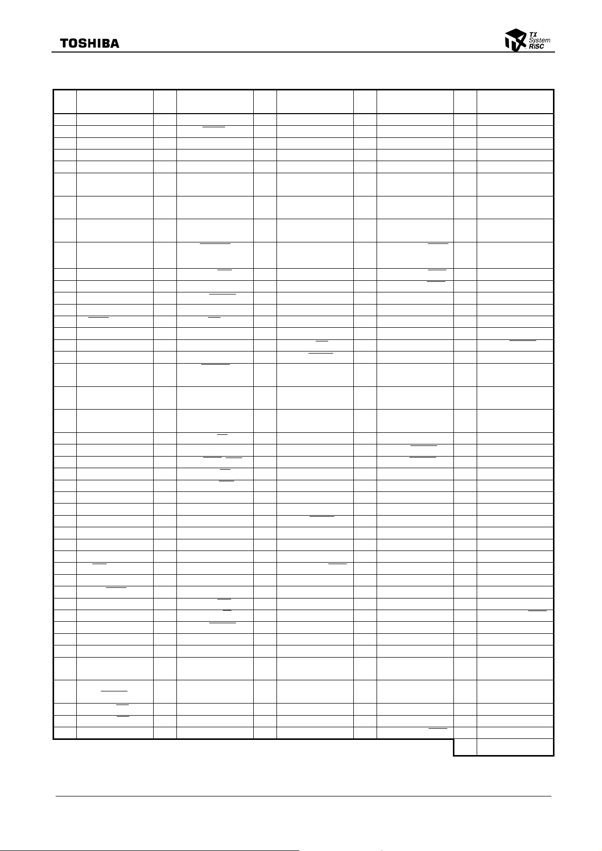
Table 2.1.2 Pin Numbers and Names (1 of 2)
Pin
No.
A1 N.C. A13 PN2 B8 P75/AN5 C2 PCST3 (EJTAG) C14 PM7
A2 VREFL A14 PN0 B9 PL0 C3 P92/AN18 C15 PM3
A3 P90/AN16 A15 PM5 B10 PL3 C4 P95/AN21 C16 PK3/KEY3
A4 P93/AN19 A16 PM1 B11 PO5/TXD6 C5 P82/AN10 C17 CVCC15
A5 P80/AN8 A17 X2 B12 PO1/INT1 C6 P85/AN13 C18 XT2
A6 P83/AN11 B1 AVCC31 B13 PN3 C7 P72/AN2 D1 TDO (EJTAG)
A7 P70/AN0 B2 VREFH B14 PN1 C8 AVSS D2 PCST2 (EJTAG)
A8 P74/AN4 B3 P91/AN17 B15 PM4 C9 PL1 D3 DINT (EJTAG)
A9 PO7/SCLK6/CTS6 B4 P94/AN20 B16 PM0 C10 PL4 D4 DVCC15
A10 PL2 B5 P81/AN9 B17 CVSS/BVSS C11 PO4/INT4 D5 P96/AN22
A11 PO6/RXD6 B6 P84/AN12 B18 X1 C12 PN6 D6 P86/AN14
A12 PO0/INT0 B7 P71/AN1 C1 PCST0 (EJTAG) C13 PN4 D7 P73/AN3
Pin name
Pin
No.
Pin name
Pin
No.
Pin name
Pin
No.
Pin name
Pin
No.
Pin name
TMP19A64(rev1.1)2-1
TMP19A64F20AXBG
Table 2.1.1 Pin Numbers and Names (2 of 2)
Pin
No.
D8 DVCC15 F18 P46/SCOUT K14 PI1/INT1 N18 P14/D12/AD12/A12 T8 PD4/TXD4
D9 DVSS G1 RESET K15 PI3/INT3 P1 PE4 T9 PC0/TXD0
D10 PL5 G2 TDI (EJTAG) K16 PI4/INT4 P2 PA2/TB0OUT T10 PC3/TXD1
D11 PO3/INT3 G3 FVCC15 K17 DVCC30 P3 PA3/TB1IN0/INT7 T11 PH4/TCOUT8
D12 PN7 G4 DVSS K18 PI2/INT2 P4 PA4/TB1IN1/INT8 T12 PH6
D13 PN5 G5 TOVR/TSTA
D14 PM2 G6 BW0 L2 PQ1/TPD1/TPC1
D15 DVCC34 G13 PK7/KEY7 L3 PQ2/TPD2/TPC2
D16 PK2/KEY2 G14 BRESET L4 PQ3/TPD3/TPC3
D17 PK4/KEY4 G15 P41/CS1 L5 PE6/INTA P9 PC2/SCLK0/CTS0 T17 P00/D0/AD0
D18 XT1 G16 P37/ALE L6 PE7/INTB P10 PC5/SCLK1/CTS1 T18 P01/D1/AD1
E1 DCLK (EJTAG) G17 P35/BUSAK L13 P13/D11/AD11/A11 P11 P52/A2 U1 PB4/TB8OUT
E2 PCST1 (EJTAG) G18 FVCC15 L14 P17/D15/AD15/A15 P12 P62/A10 U2 PB3/TB7OUT
E3 TRST (EJTAG) H1 NMI L15 FVCC15 P13 P65/A13 U3 PB7/TBAIN1
E4 PCST4 (EJTAG) H2 DVCC31 L16 PI0/INT0 P14 P26/A22/A6/A22 U4 PF1/SI/SCL
E5 ENDIAN H3 PP7/TPD7 (EJTAG) L17 P45/CS5 P15 P02/D2/AD2 U5 PF5/DREQ3
E6 P97/AN23 H4 BW1 L18 PJ3/DACK3 P16 P10/D8/AD8/A8 U6 PG1/TC1IN
E7 P87/AN15 H5 PLLOFF M1 PQ0/TPD0/TPC0
E8 P76/AN6 H6 TCK (EJTAG) M2 PQ7/TPD7/TPC7
E9 P77/AN7 H13 TEST1 M3 PQ4/TPD4/TPC4
E10 PL6 H14 P31/WR M4 PE3 R2 PA1/TB0IN1/INT6 U10 PH1/TCOUT5
E11 PL7 H15 P32/HWR M5 PA7/TB3OUT R3 PF3/DREQ2 U11 PH5/TCOUT9
E12 PM6 H16 P33/WAIT/RDY M6 DVCC32 R4 PF4/DACK2 U12 P50/A0
E13 PK6/KEY6 H17 P30/RD M13 P06/D6/AD6 R5 PF7/TBTIN U13 P55/A5
E14 PK5/KEY5 H18 P40/CS0 M14 P07/D7/AD7 R6 PG7/TCOUT3 U14 DVCC33
E15 BVCC J1 PP2/TPD2 (EJTAG) M15 DVSS R7 PG4/TCOUT0 U15 P64/A12
E16 PK1/KEY1 J2 PP3/TPD3 (EJTAG) M16 PJ0/DREQ2 R8 PD5/RXD4 U16 P20/A16/A0/A16
E17 PK0/KEY0 J3 PP4/TPD4 (EJTAG) M17 PJ2/DREQ3 R9 PC1/RXD0 U17 P24/A20/A4/A20
E18 DVCC15 J4 PP5/TPD5 (EJTAG) M18 PJ1/DACK2 R10 PC4/RXD1 U18 FVCC3
F1 DVSS J5 PP6/TPD6 (EJTAG) N1 PE5 R11 PH3/TCOUT7 V2 PB5/TB9OUT
F2 TMS (EJTAG) J6 FVCC15 N2 PE0/TXD5 R12 P51/A1 V3 PG0/TC0IN
F3 EJE (EJTAG) J13 DVSS N3 PE2/SCLK5/CTS5 R13 P57/A7 V4 PF0/SO/SDA
F4 BUSMD J14 P47 N4 PE1/RXD5 R14 P66/A14 V5 PG3/TC3IN
F5 BOOT J15 N.C. N5 PA6/TB2OUT R15 P25/A21/A5/A21 V6 PG6/TCOUT2
F7 AVSS J16 P44/CS4 N7 DVSS R16 P03/D3/AD3 V7 PD1/TXD3
F8 AVSS J17 P36/ R/W N8 PD7/INT9 R17 P04/D4/AD4 V8 PD0/SCLK2/CTS2
F9 AVCC32 J18 P34/BUSRQ N9 DVCC15 R18 P05/D5/AD5 V9 PC6/TXD2
F10 DVCC34 K1 PP0/TPD0 (EJTAG) N10 DVSS T1 PB0/TB4OUT V10 PH2/TCOUT6
F11 PO2/INT2 K2 PP1/TPD1 (EJTAG) N11 P56/A6 T2 PB1/TB5OUT V11 PH0/TCOUT4
F12 DVSS K3 PQ5/TPD5/TPC5
F14
F15 P42/CS2 K5 DVSS N15 P15/D13/AD13/A13 T5 PF6/DACK3 V14 P60/A8
F16 P43/CS3 K6 DVSS N16 TEST3 T6 PG5/TCOUT1 V15 P63/A11
F17 DVCC33 K13 TEST2 N17 P16/D14/AD14/A14 T7 PD3/SCLK3/CTS3 V16 P67/A15
Pin name
BUPMD
V17 P22/A18/A2/A18
Pin
No.
K4 PQ6/TPD6/TPC6
Pin name
(EJTAG)
(EJTAG)
(EJTAG)
Pin
No.
L1 FVCC3 P5 PA5/TB1OUT T13 P53/A3
N12 DVSS T3 PB2/TB6OUT V12 PH7
N14 P27/A23/A7/A23 T4 PF2/SCK V13 P54/A4
Pin name
(EJTAG)
(EJTAG)
(EJTAG)
(EJTAG)
(EJTAG)
(EJTAG)
Pin
No.
P6 PB6/TBAIN0 T14 P61/A9
P7 PG2/TC2IN T15 P21/A17/A1/A17
P8 PD6/SCLK4/CTS4 T16 P23/A19/A3/A19
P17 P12/D10/AD10/A10 U7 PD2/RXD3
P18 P11/D9/AD9/A9 U8 DVCC32
R1 PA0/TB0IN0/INT5 U9 PC7/RXD2
Pin name
Pin
No.
Pin name
TMP19A64(rev1.1)2-2

2.2 Pin Names and Functions
Table 2.2.1 shows the names and functions of input/output pins.
Table 2.2.1 Pin Names and Functions (1 of 6)
Pin name
P00-P07
D0-D7
AD0-AD7
P10-P17
D8-D15
AD8-AD15
A8-A15
P20-P27
A16-A23
A0-A7
A16-A23
P30
RD
P31
WR
P32
HWR
P33
WAIT
RDY
P34
BUSRQ
P35
BUSAK
P36
R/W
P37
ALE
P40
CS0
P41
CS1
P42
CS2
P43
CS3
P44
CS4
P45
CS5
P46
SCOUT
P47 1 Input/output Port 47: Input/output port
P50-P57
A0-A7
P60-P67
A8-A15
Number
of pins
8 Input/output
8 Input/output
8 Input/output
1 Output
1 Output
1 Input/output
1 Input/output
1 Input/output
1 Input/output
1 Input/output
1 Input/output
1 Input/output
1 Input/output
1 Input/output
1 Input/output
1 Input/output
1 Input/output
1 Input/output
8 Input/output
8 Input/output
Input or
output
Input/output
Input/output
Input/output
Input/output
Output
Output
Output
Output
Output
Output
Output
Input
Input
Input
Output
Output
Output
Output
Output
Output
Output
Output
Output
Output
Output
Output
Port 0: Input/output port that allows input/output to be set in units of bits
Data (lower): Data buses 0 to 7 (separate bus mode)
Address data (lower): Address data buses 0 to 7 (multiplexed bus mode)
Port 1: Input/output port that allows input/output to be set in units of bits
Data (upper): Data buses 8 to 15 (separate bus mode)
Address data (upper): Address data buses 8 to 15 (multiplexed bus mode)
Address: Address buses 8 to 15 (multiplexed bus mode)
Port 2: Input/output port that allows input/output to be set in units of bits
Address: Address buses 16 to 23 (separate bus mode)
Address: Address buses 0 to 7 (multiplexed bus mode)
Address: Address buses 16 to 23 (multiplexed bus mode)
Port 30: Port used exclusively for output
Read: Strobe signal for reading external memory
Port 31: Port used exclusively for output
Write: Strobe signal for writing data of D0 to D7 pins
Port 32: Input/output port (with pull-up)
Write upper-pin data: Strobe signal for writing data of D8 to D15 pins
Port 33: Input/output port (with pull-up)
Wait: Pin for requesting CPU to put a bus in a wait state
Ready: Pin for notifying CPU that a bus is ready
Port 34: Input/output port (with pull-up)
Bus request: Signal requesting CPU to allow an external master to take the bus control authority
Port 35: Input/output port (with pull-up)
Bus acknowledge: Signal notifying that CPU has released the bus control authority in response
to BUSRQ
Port 36: Input/output port (with pull-up)
Read/write: "1" shows a read cycle or a dummy cycle. "0" shows a write cycle.
Port 37: Input/output port
Address latch enable (address latch is enabled only if access to external memory is taking place)
Port 40: Input/output port (with pull-up)
Chip select 0: "0" is output if the address is in a designated address area.
Port 41: Input/output port (with pull-up)
Chip select 1: "0" is output if the address is in a designated address area.
Port 42: Input/output port (with pull-up)
Chip select 2: "0" is output if the address is in a designated address area.
Port 43: Input/output port (with pull-up)
Chip select 3: "0" is output if the address is in a designated address area.
Port 44: Input/output port (with pull-up)
Chip select 4: "0" is output if the address is in a designated address area.
Port 45: Input/output port (with pull-up)
Chip select 5: "0" is output if the address is in a designated address area.
Port 46: Input/output port
System clock output: Selectable between high- and low-speed clock outputs, as in the case of
CPU
Port 5: Input/output port that allows input/output to be set in units of bits
Address: Address buses 0 to 7 (separate bus mode)
Port 6: Input/output port that allows input/output to be set in units of bits
Address: Address buses 8 to 15 (separate bus mode)
TMP19A64F20AXBG
Function
TMP19A64(rev1.1)2-3
Pin name
P70-P77
AN0-AN7
P80-P87
AN8-AN15
P90-P97
AN16-AN23
PA0
TB0IN0
INT5
PA1
TB0IN1
INT6
PA2
TB0OUT
PA3
TB1IN0
INT7
PA4
TB1IN1
INT8
PA5
TB1OUT
PA6
TB2OUT
PA7
TB3OUT
PB0
TB4OUT
PB1
TB5OUT
PB2
TB6OUT
PB3
TB7OUT
PB4
TB8OUT
PB5
TB9OUT
PB6
TBAIN0
PB7
TBAIN1
Number
of pins
8 Input
8 Input
8 Input
1 Input/output
1 Input/output
1 Input/output
1 Input/output
1 Input/output
1 Input/output
1 Input/output
1 Input/output
1 Input/output
1 Input/output
1 Input/output
1 Input/output
1 Input/output
1 Input/output
1 Input/output
1 Input/output
Input or
output
Input
Input
Input
Input
Input
Input
Input
Output
Input
Input
Input
Input
Output
Output
Output
Output
Output
Output
Output
Output
Output
Input
Input
TMP19A64F20AXBG
Table 2.2.1 Pin Names and Functions (2 of 6)
Function
Port 7: Port used exclusively for input
Analog input: Input from A/D converter
Port 8: Port used exclusively for input
Analog input: Input from A/D converter
Port 9: Port used exclusively for input
Analog input: Input from A/D converter
Port A0: Input/output port
16-bit timer 0 input 0: For inputting the count/capture trigger of a 16-bit timer 0
Interrupt request pin 5: Selectable between "H" level, "L" level, rising edge, and falling edge
Input pin with Schmitt trigger
Port A1: Input/output port
16-bit timer 0 input 1: For inputting the count/capture trigger of a 16-bit timer 0
Interrupt request pin 6: Selectable "H" level, "L" level, rising edge and falling edge
Input pin with Schmitt trigger
Port A2: Input/output port
16-bit timer 0 output: 16-bit timer 0 output pin
Port A3: Input/output port
16-bit timer 1 input 0: For inputting the count/capture trigger of a 16-bit timer 1
Interrupt request pin 7: Selectable between "H" level, "L" level, rising edge and falling edge
Input pin with Schmitt trigger
Port A4: Input/output port
16-bit timer 1 input 1: For inputting the count/capture trigger of a 16-bit timer 1
Interrupt request pin 8: Selectable between "H" level, "L" level, rising edge and falling edge
Input pin with Schmitt trigger
Port A5: Input/output port
16-bit timer 1 output: 16-bit timer 1 output pin
Port A6: Input/output port
16-bit timer 2 output: 16-bit timer 2 output pin
Port A7: Input/output port
16-bit timer 3 output: 16-bit timer 3 output pin
Port B0: Input/output port
16-bit timer 4 output: 16-bit timer 4 output pin
Port B1: Input/output port
16-bit timer 5 output: 16-bit timer 5 output pin
Port B2: Input/output port
16-bit timer 6 output: 16-bit timer 6 output pin
Port B3: Input/output port
16-bit timer 7 output: 16-bit timer 7 output pin
Port B4: Input/output port
16-bit timer 8 output: 16-bit timer 8 output pin
Port B5: Input/output port
16-bit timer 9 output: 16-bit timer 9 output pin
Port B6: Input/output port
16-bit timer A input 0: for inputting the count/capture trigger of a 16-bit timer A
2-phase pulse counter input 0
Port B7: Input/output port
16-bit timer A input 1: For inputting the count/capture trigger of a 16-bit timer A
2-phase pulse counter input 1
TMP19A64(rev1.1)2-4
Pin name
PC0
TXD0
PC1
RXD0
PC2
SCLK0
CTS0
PC3
TXD1
PC4
RXD1
PC5
SCLK1
CTS1
PC6
TXD2
PC7
RXD2
PD0
SCLK2
CTS2
PD1
TXD3
PD2
RXD3
PD3
SCLK3
CTS3
PD4
TXD4
PD5
RXD4
PD6
SCLK4
CTS4
PD7
INT9
Number
of pins
1 Input/output
1 Input/output
1 Input/output
1 Input/output
1 Input/output
1 Input/output
1 Input/output
1 Input/output
1 Input/output
1 Input/output
1 Input/output
1 Input/output
1 Input/output
1 Input/output
1 Input/output
1 Input/output
Input or
output
Output
Input
Input/output
Input
Output
Input
Input/output
Input
Output
Input
Input/output
Input
Output
Input
Input/output
Input
Output
Input
Input/output
Input
Input
TMP19A64F20AXBG
Table 2.2.1 Pin Names and Functions (3 of 6)
Function
Port C0: Input/output port
Sending serial data 0: Open drain output pin depending on the program used
Port C1: Input/output port
Receiving serial data 0
Port C2: Input/output port
Serial clock input/output 0
Ready to send serial data 0 (Clear To Send): Open drain output pin depending on the program
used
Port C3: Input/output port
Sending serial data 1: Open drain output pin depending on the program used
Port C4: Input/output port
Receiving serial data 1
Port C5: Input/output port
Serial clock input/output 1
Ready to send serial data 1 (Clear To Send): Open drain output pin depending on the program
used
Port C6: Input/output port
Sending serial data 2: Open drain output pin depending on the program used
Port C7: Input/output port
Receiving serial data 2
Port D0: Input/output port
Serial clock input/output 2
Ready to send serial data 2 (Clear To Send): Open drain output pin depending on the program
used
Port D1: Input/output port
Sending serial data 3: Open drain output pin depending on the program used
Port D2: Input/output port
Receiving serial data 3
Port D3: Input/output port
Serial clock input/output 3
Ready to send serial data 3 (Clear To Send): Open drain output pin depending on the program
used
Port D4: Input/output port
Sending serial data 4: Open drain output pin depending on the program used
Port D5: Input/output port
Receiving serial data 4
Port D6: Input/output port
Serial clock input/output 4
Ready to send serial data 4 (Clear To Send): Open drain output pin depending on the program
used
Port D7: Input/output port
Interrupt request pin 9: Selectable between "H" level, "L" level, rising edge and falling edge
Input pin with Schmitt trigger
TMP19A64(rev1.1)2-5

TMP19A64F20AXBG
Table 2.2.1 Pin Names and Functions (4 of 6)
Pin name
PE0
TXD5
PE1
RXD5
PE2
SCLK5
CTS5
PE3-PE5 3 Input/output Ports E3 to E5: Input/output ports that allow input/output to be set in units of bits
PE6
INTA
PE7
INTB
PF0
SO
SDA
PF1
SI
SCL
PF2
SCK
PF3
DREQ2
PF4
DACK2
PF5
DREQ3
PF6
DACK3
PF7
TBTIN
PG0-PG3
TC0IN-TC3IN
PG4-PG7
TCOU0-TCOUT3
PH0-PH5
TCOU4-TCOUT9
PH6-PH7 2 Input/output Ports H6 to H7: Input/output ports that allow input/output to be set in units of bits
PI0
INT0
PI1
INT1
PI2
INT2
Number
of pins
1 Input/output
1 Input/output
1 Input/output
1 Input/output
1 Input/output
1 Input/output
1 Input/output
1 Input/output
1 Input/output
1 Input/output
1 Input/output
1 Input/output
1 Input/output
4 Input/output
4 Input/output
6 Input/output
1 Input/output
1 Input/output
1
Input or
output
Output
Input
Input/output
Input
Input
Input
Output
Input/output
Input
Input/output
Input/output
Input
Output
Input
Output
Input
Input
Output
Output
Input
Input
Input/output
Input
Function
Port E0: Input/output port
Sending serial data 5: Open drain output pin depending on the program used
Port E1: Input/output port
Receiving serial data 5
Port E2: Input/output port
Serial clock input/output 5
Ready to send serial data 5 (Clear To Send): Open drain output pin depending on the program
used
Port E6: Input/output port
Interrupt request pin A: Selectable between "H" level, "L" level, rising edge, and falling edge
Input pin with Schmitt trigger
Port E7: Input/output port
Interrupt request pin B: Selectable between "H" level, "L" level, rising edge, and falling edge
Input pin with Schmitt trigger
Port F0: Input/output port
Pin for sending data if the serial bus interface operates in the SIO mode
Pin for sending and receiving data if the serial bus interface operates in the I
Open drain output pin depending on the program used.
Input with Schmitt trigger
Port F1: Input/output port
Pin for receiving data if the serial bus interface operates in the SIO mode
Pin for inputting and outputting a clock if the serial bus interface operates in the I
Open drain output pin depending on the program used
Input with Schmitt trigger
Port F2: Input/output port
Pin for inputting and outputting a clock if the serial bus interface operates in the SIO mode
Port F3: Input/output port
DMA request signal 2: For inputting the request to transfer data by DMA from an external I/O
device to DMAC2
Port F4: Input/output port
DMA acknowledge signal 2: Signal showing that DREQ2 has acknowledged a DMA transfer
request
Port F5: Input/output port
DMA request signal 3: For inputting the request to transfer data by DMA from an external I/O
device to DMAC3
Port F6: Input/output port
DMA acknowledge signal 3: Signal showing that DREQ3 has acknowledged a DMA transfer
request
Port F7: Input/output port
32-bit time base timer input: For inputting the count for 32-bit time base timer
Ports G0 to G3: Input/output ports that allow input/output to be set in units of bits
For inputting the capture trigger for 32-bit timer
Ports G4 to G7: Input/output ports that allow input/output to be set in units of bits
Outputting 32-bit timer if the result of a comparison is a match
Ports H0 to H5: Input/output ports that allow input/output to be set in units of bits
Outputting 32-bit timber if the result of a comparison is a match
Port I0: Input/output port
Interrupt request pin 0: Selectable between "H" level, "L" level, rising edge and falling edge
Input pin with Schmitt trigger
Port I1: Input/output port
Interrupt request pin 1: Selectable between "H" level, "L" level, rising edge and falling edge
Input pin with Schmitt trigger
Port I2: Input/output port
Interrupt request pin 2: Selectable between "H" level, "L" level, rising edge and falling edge
Input pin with Schmitt trigger
2
C mode
2
C mode
TMP19A64(rev1.1)2-6

TMP19A64F20AXBG
Table 2.2.1 Pin Names and Functions (5 of 6)
Pin name
PI3
INT3
PI4
INT4
PJ0
DREQ2
PJ1
DACK2
PJ2
DREQ3
PJ3
DACK3
PK0-PK7
KEY0-KEY7
PL0-PL7 8 Input/output Port L: Input/output port that allows input/output to be set in units of bits
PM0-PM7 8 Input/output Port M: Input/output port that allows input/output to be set in units of bits
PN0-PN7 8 Input/output Port N: Input/output port that allows input/output to be set in units of bits
PO0
INT0
PO1
INT1
PO2
INT2
PO3
INT3
PO4
INT4
PO5
TXD6
PO6
RXD6
PO7
SCLK6
CTS6
PP0-PP7
TPD0-TPD7
PQ0-PQ7
TPC0-TPC7
TPD0-TPD7
Number
of pins
Input or output Function
1 Input/output
Input
1 Input/output
Input
1 Input/output
Input
1 Input/output
Output
1 Input/output
Input
1 Input/output
Output
8 Input/output
Input
1 Input/output
Input
1 Input/output
Input
1 Input/output
Input
1 Input/output
Input
1 Input/output
Input
1 Input/output
Output
1 Input/output
Input
1 Input/output
Input/output
Input
8 Input/output
Output
8 Input/output
Output
Output
Port I3: Input/output port
Interrupt request pin 3: Selectable between "H" level, "L" level, rising edge and falling edge
Input pin with Schmitt trigger
Port I4: Input/output port
Interrupt request pin 4: Selectable between "H" level, "L" level, rising edge and falling edge
Input pin with Schmitt trigger
Port J0: Input/output port
DMA request signal 2: For inputting the request to transfer data by DMA from an external I/O
device to DMAC2
Port J1: Input/output port
DMA acknowledge signal 2: Signal showing that DREQ2 has acknowledged a DMA transfer
request
Port J2: Input/output port
DMA request signal 3: For inputting the request to transfer data by DMA from an external I/O
device to DMAC3
Port J3: Input/output port
DMA acknowledge signal 3: Signal showing that DREQ3 has acknowledged a DMA transfer
request
Port K: Input/output port that allows input/output to be set in units of bits
KEY on wake up input 0 to 7 (with pull-up)
With Schmitt trigger
Port O0: Input/output port
Interrupt request pin 0: Selectable between "H" level, "L" level, rising edge and falling edge
Input pin with Schmitt trigger
Port O1: Input/output port
Interrupt request pin 1: Selectable between "H" level, "L" level, rising edge and falling edge
Input pin with Schmitt trigger
Port O2: Input/output port
Interrupt request pin 2: Selectable between "H" level, "L" level, rising edge and falling edge
Input pin with Schmitt trigger
Port O3: Input/output port
Interrupt request pin 3: Selectable between "H" level, "L" level, rising edge and falling edge
Input pin with Schmitt trigger
Port O4: Input/output port
Interrupt request pin 4: Selectable between "H" level, "L" level, rising edge and falling edge
Input pin with Schmitt trigger
Port O5: Input/output port
Sending serial data 6: Open drain output pin depending on the program used
Port O6: Input/output port
Receiving serial data 6
Port O7: Input/output port
Serial clock input/output 6
Ready to send serial data 6 (Clear To Send): Open drain output pin depending on the program
used
Port P: Input/output port that allows input/output to be set in units of bits
Outputting trace data from the data access address: Signal for DSU-ICE
Port P: Input/output port that allows input/output to be set in units of bits
Outputting trace data from the program counter: Signal for DSU-ICE
Outputting trace data from the data access address: Signal for DSU-ICE
TMP19A64(rev1.1)2-7

TMP19A64F20AXBG
Table 2.2.1 Pin Names and Functions (6 of 6)
Pin name
DCLK 1 Output Debug clock: Signal for DSU-ICE
EJE 1 Input EJTAG enable: Signal for DSU-ICE (input with Schmitt trigger and built-in noise filter)
PCST4-0 5 Output PC trace status: Signal for DSU-ICE
DINT 1 Input Debug interrupt: Signal for DSU-ICE
TOVR/TSTA 1 Output Outputting the status of PD data overflow status: Signal for DSU-ICE
TCK 1 Input Test clock input: Signal for testing JTAG (input with Schmitt trigger and pull-up)
TMS 1 Input Test mode select input: Signal for testing JTAG (input with Schmitt trigger and pull-up)
TDI 1 Input Test data input: Signal for testing JTAG (input with Schmitt trigger and pull-up)
TDO 1 Output Test data output: Signal for testing JTAG
TRST 1 Input Test reset input: Signal for testing JTAG (input with Schmitt trigger and pull-down)
NMI 1 Input Nonmaskable interrupt request pin: Pin for requesting an interrupt at the falling edge
PLLOFF 1 Input Fix this pin to the "H (DVCC15) level."(Input with Schmitt trigger)
RESET 1 Input Reset: Initializing LSI (with pull-up)
X1/X2 2 Input/output Pin for connecting to a high-speed oscillator
XT1/XT2 2 Input/output Pin for connecting to a low-speed oscillator
BUPMD 1 Input Backup mode trigger pin: This pin must be set to "L level" in backup mode.
BRESET 1 Input Backup module reset: Initializing the backup module (with pull-up)
BUSMD 1 Input Pin for setting an external bus mode: This pin functions as a multiplexed bus by sampling the
ENDIAN 1 Input Pin for setting endian: This pin is used to set a mode. It performs a big-endian operation by
BOOT 1 Input Pin for setting a single boot mode: This pin goes into single boot mode by sampling "L" upon
BW0-1 2 Input
VREFH 1 Input Pin (H) for supplying the A/D converter with a reference power supply
VREFL 1 Input Pin (L) for supplying the A/D converter with a reference power supply
AVCC31-32 2
AVSS 3
TEST1-3 3 Input TEST pin: To be fixed to GND.
CVCC15 1
CVSS/BVSS 1
DVCC15 4
BVCC 1
DVCC30-34 8
DVSS 11
FVCC15 4
FVCC3 2
Number
of pins
Input or output Function
(input with Schmitt trigger, pull-up and built-in noise filter)
Input with Schmitt trigger and built-in noise filter
Input with Schmitt trigger and built-in noise filter
Input with Schmitt trigger
"H (DVCC15) level" upon the rising of a reset signal. It also functions as a separate bus by
sampling "L" upon the rising of a reset signal. When performing a reset operation, pull it up or
down according to a bus mode to be used.
sampling the "H (DVCC15) level" upon the rising of a reset signal, and performs a littleendian operation by sampling "L" upon the rising of a reset signal. When performing a reset
operation, pull it up or down according to the type of endian to be used.
the rising of a reset signal. It is used to overwrite internal flash memory. By sampling "H
(DVCC15) level" upon the rising of a reset signal, it performs a normal operation. This pin
should be pulled up under normal operating conditions. Pull it up when resetting.
Fix these pins to BW0="H (DVCC15)" and BW1="H (DVCC15)," respectively.
(Input with Schmitt trigger)
Connect this pin to AVCC31 if the A/D converter is not used.
Connect this pin to AVSS if the A/D converter is not used.
−
−
−
−
−
−
−
−
−
−
Pin for supplying the A/D converter with a power supply. Connect it to a power supply even if
the A/D converter is not used.
A/D converter GND pin (0 V). Connect this pin to GND even if the A/D converter is not used.
Pin for supplying oscillators with power: 1.5 V power supply
GND pin (0 V) for oscillators and backup modules
Power supply pin: 1.5 V power supply
Pin exclusively for supplying backup modules with power: 3 V power supply
Power supply pin: 3 V power supply
GND pin (0 V)
Power supply pin: 1.5 V power supply
Power supply pin: 3 V power supply
TMP19A64(rev1.1)2-8

TMP19A64F20AXBG
Note 1: For BUSMD, ENDIAN and BOOT pins, the state designated for each pin ("H" or "L"
level) must be maintained during one system clock before and after the rising of a
reset signal. The reset pin must always be in a stable state at both "L" and "H" levels.
Note 2: For DREQ2, DACK2, DREQ3 and DACK3, it is necessary to go to the port function
register and to select one port from two groups of ports, PF3 to PF6 and PJ0 to PJ3.
Two ports cannot be operated simultaneously to use the same function.
Likewise, for pins INT0 through INT4, one port must be selected from ports PI0 to PI4
and ports PO0 to PO4.
Table 2.2.2 shows the pin names and power supply pins.
Table 2.2.2 Pin names and power supply pins
Power
Pin name
P0 DVCC33 PCST4 to 0 DVCC31
P1 DVCC33 DCLK DVCC31
P2 DVCC33 EJE DVCC31
P3 DVCC33 TRST DVCC31
P4 DVCC33 TDI DVCC31
P5 DVCC33 TDO DVCC31
P6 DVCC33 TMS DVCC31
P7 AVCC32 TCK DVCC31
P8 AVCC32 DINT DVCC31
P9 AVCC31 TOV DVCC31
PA DVCC32 BUSMD DVCC15
PB DVCC32 BOOT DVCC15
PC DVCC32 ENDIAN DVCC15
PD DVCC32 NMI DVCC15
PE DVCC32 BRESET BVCC
PF DVCC32 BUPMD BVCC
PG DVCC32 X1, X2 CVCC15
PH DVCC32 XT1, XT2 BVCC
PI DVCC30 BW0 and 1 DVCC15
PJ DVCC33 PLLOFF DVCC15
PK DVCC34 RESET DVCC15
PL DVCC34
PM DVCC34
PN DVCC34
PO DVCC34
PP DVCC31
PQ DVCC31
z 2.7 V ≤ AVCC32 ≤ A VCC31
supply pin
Pin name
Power
supply pin
TMP19A64(rev1.1)2-9

TMP19A64F20AXBG
Table 2.2.3 shows the pin numbers and power supply pins.
Table 2.2.3 Pin numbers and power supply pins
Power
supply pin
DVCC15 D4, D8, E18, N9 1.35 V to 1.65 V
CVCC15 C17 1.35 V to 1.65 V
DVCC30 K17 1.65 V to 3.3 V
DVCC31 H2 1.65 V to 3.3 V
DVCC32 M6, U8 1.65 V to 3.3 V
DVCC33 F17, U14 1.65 V to 3.3 V
DVCC34 D15, F10 1.65 V to 3.3 V
AVCC31 B1 2.7 V to 3.3 V
AVCC32 F9 2.7 V to 3.3 V
FVCC15 G3, G18, J6, L15 1.35 V to 1.65 V
FVCC3 L1, U18 2.7 V to 3.3 V
BVCC E15 2.3 V to 3.3 V
Pin number Voltage range
(under normal operating conditions)
1.8 V to 3.3 V (in BACKUP mode)
TMP19A64(rev1.1)2-10

3. Flash Memory Operation
This section describes the hardware configuration and operation of the flash memory. The feature of this device
is that the internal ROM of TMP19A64C1DXBG is replaced by an internal flash memory. Other configurations
and functions of the device remain the same as with TMP19A64C1DXBG. Please refer to the
TMP19A64C1DXBG data sheet for functions not described in this section.
3.1 Flash Memory
3.1.1 Features
1) Memory capacity
The TMP19A64F20AXBG device contains two 8M bits (1MB) of flash memory capacity. The
memory area consists of 4 independent memory blocks (128 kB × 16) to enable independent write
access to each block. When the CPU is to access the internal flash memory, 32-bit data bus width
is used.
2) Write/erase
Write unit: 1 page (128 words) × 4k
Erase unit: Selectable from 128 KB, 512 KB, and 1 MB
Protection unit: Selectable in 512 KB blocks
Protection erasure unit: Selectable in 1 MB blocks
3) Write/erase time
Write time: 8 sec/2 chip (Typ) 2 msec/128 word (Typ.)
Erase time: 1.6 sec /2 chip (Typ) 100 msec/128 Kbyte (Typ.)
Protection bit erase time: 100 msec/2 bit (Typ)
(Note) The above values are theoretical values not including data transfer time.
The write time per chip depends on the write method to be used by the user.
4) Programming method
Two modes are available, i.e., the onboard programming mode to allow programming on the
user's board and the writer mode to program the device using an EPROM writer.
TMP19A64F20AXBG
Onboard programming mode 1) User boot mode
•
2) Single boot mode
The rewriting method to use serial data transfer
(Toshiba's unique method) can be supported.
Writer mode
•
Use of a general purpose EPROM writer is supported.
5) Rewriting method
The flash memory included in this device is generally compliant with the applicable JEDEC
standards except for some specific functions. Therefore, if the user is currently using an external
flash memory device, it is easy to implement the functions into this device. Furthermore, the user
is not required to build his/her own programs to realize complicated write and erase functions
because such functions are automatically performed using the circuits already built-in the flash
memory chip.
This device is also implemented with a read-security function to inhibit reading flash memory
data from any external writer device. On the other hand, rewrite protection is available only
through command-based software programming; any hardware setting method to apply +12VDC
is not supported. The above described security function is automatically enabled when all the four
area are configured for protection. When the user removes protection, the internal data is
automatically erased before the protection is actually removed.
The user's original rewriting method can be supported.
TMP19A64(rev1.1)-3-1

JEDEC compliant functions Modified, added, or deleted functions
• Automatic programming
• Automatic chip erase
• Automatic block erase
• Data polling/toggle bit
3.1.2 Block Diagram
TMP19A64F20AXBG
<Modified> Block protect (only software protection is supported)
<Deleted> Erase resume - suspend function
Automatic multiple block erase (supported to the chip
level)
Internal address bus
Internal data bus
Internal control bus
ROM controller
Control Address Data
Control
circuit
(includes
automatic
sequence
control)
Command
register
Column decoder/sense amplifier
Flash memory cell
1MB 1MB
Row decoder
Erase block decoder
Fig. 3.1.2.1 Block Diagram of the Flash Memory Section
Data latchAddress latch
Flash Memory
Row decoder
TMP19A64(rev1.1)-3-2

TMP19A64F20AXBG
3.2 Operation Mode
This device has four operation modes including the mode not to use the internal flash memory.
Table 3.2.1.1 Operation Modes
Operation mode Operation details
Single chip mode
Normal mode
User boot mode The user can uniquely configure the system to switch between these two modes.
Single boot mode
Writer mode
Among the flash memory operation modes listed in the above table, the user boot mode, single boot mode, and
writer mode are programmable modes. These two modes, the User Boot mode and the Single Boot mode, are
referred to as "Onboard Programming" modes where onboard rewriting of internal flash memory can be made
on the user's card.
After reset is cleared, it starts up from the internal flash memory.
In this operation mode, two different modes, i.e., the mode to execute user application programs
and the mode to rewrite the flash memory onboard the user’s card, are defined. The former is
referred to as "normal mode" and the latter "user boot mode."
For example, the user can freely design the system such that the normal mode is selected when the
port "00" is set to "1" and the user boot mode is selected when it is set to "0."
The user should prepare a routine as part of the application program to make the decision on the
selection of the modes.
After reset is cleared, it starts up from the internal Boot ROM (Mask ROM). In the Boot ROM, an
algorithm to enable flash memory rewriting on the user’s set through the serial port of this device
is programmed. By connecting to an external host computer through the serial port, the internal
flash memory can be programmed by transferring data in accordance with predefined protocols.
This mode allows use of a general purpose EPROM writer to rewrite the internal flash memory.
Please use a special program adaptor and an EPROM writer that are recommended for use.
TMP19A64(rev1.1)-3-3

TMP19A64F20AXBG
g
Either the single chip, single boot, or writer operation mode can be selected by externally setting the levels of
the BW0, BW1, and
BOOT input pins while the device is in the reset state.
Except for the case of the writer mode, the CPU starts operation in the selected operation mode when the reset
condition is removed after the pin levels are set. The writer mode is used with
RESET set to "0". Be sure not to
change the levels during operation once the mode is selected. The mode setting method and the mode transition
diagram are shown below:
Table 3.2.1.2 Operation Mode Setting
Operation mode
(1) Single chip mode
(2) Single boot mode
(3) Writer mode *1 *1 *1 *1
RESET
0 → 1
0 → 1
Input pin
BW0 BW1
1 1 1
1 1 0
BOOT
*1: Don't care (No explanation is given in this section regarding condition settings.)
Writer mode
(3)
Reset mode
Single chip mode
Normal mode
Boot mode
User
(1)
/
RESET = 0
Single
Boot mode
(2)
RESET = 0
/
The number in the parentheses indicate the mode number in the above table to
show the input pin setting to be made for the corresponding state transition.
User to set the
switch method
Onboard
ramming mode
Pro
Fig. 3.2.1.3 Mode Transitio n Diagram
3.2.1 Reset Operation
To reset the device, ensure that the power supply voltage is within the operating voltage range, that the
internal oscillator has been stabilized, and that the
RESET
12 system clocks (1.8 μs with 54 MHz operation; the "1/8" clock gear mode is applied after reset).
(Note 1) Regarding power-on reset of devices with internal flash memory;
For devices with internal flash memory, it is necessary to apply "0" to the
upon power on for a minimum duration of 60 microseconds regardless of the operating
frequency.
During this period, each protection bit, to be described later, is locked in the state it is
written regardless of the state it ought to be. The original values of protection bits can be
checked by reading the register FLCS <BLPRO 3:0> after the power on reset operation is
normally terminated.
(Note 2) While flash programming is in progress, at least 0.5 microseconds of reset period is
required regardless of the system clock frequency.
TMP19A64(rev1.1)-3-4
input is held at "0" for a minimum duration of
RESET inputs

TMP19A64F20AXBG
3.2.2 DSU (EJTAG) - PROBE Interface
This interface is used when the DSU probe is used in debugging. This is the dedicated interface for
connection to the DSU probe. Please refer to the operation manual for the DSU probe you are going to use
for details of debugging procedures to use the DSU probe. Here, the function to enable/disable the DSU
probe in the DSU (EJTAG) mode is described.
1) Security function
This device allows use of an on-board DSU probe for debugging. To facilitate this, the device is
implemented with a security measure to prevent easy reading of the internal flash memory by a third
party other than the authorized user. By enabling the security function, it becomes impossible to read
the internal flash memory from a DSU probe. Use this function together with the security function of
the internal flash memory itself as described later.
2) DSU probe enable/disable function
This device allows use of on-board DSU probes for debugging operations. To facilitate this, the device
is implemented with the "DSU probe inhibit" function (hereafter referred to as the "DSU inhibit"
function) to prevent easy reading of the internal flash memory by a third party other than the
authorized user. By enabling the DSU inhibit function, use of any DSU probe becomes impossible.
3) DSU enable (Enables use of DSU probes for debugging)
In order to prevent the DSU inhibit function from being accidentally removed by system runaway, etc.,
the method to cancel the inhibit function requires a double action operation so it is necessary to set
DSU security mode register DSUSEC1<DSUOFF> to "0" and also write the security code
"0x0000_00C5" to the DSU security control register DSUSEC2 to cancel the function. Then,
debugging to use a DSU probe is allowed. While power to the device is still applied, setting
DSUSEC1<DSUOFF> to "1" and writing "0x0000_00C5" to the DSUSEC2 register will enable the
security function again.
Table 3.2.2.1 DSU Security Mode Register
7 6 5 4 3 2 1 0
DSUSEC1 Bit Symbol DSUOFF
(0xFFFF_E510) Read/Write R R/W
After power
Function Always reads "0." 1: DSU disable
15 14 13 12 11 10 9 8
Bit Symbol
Read/Write R
After power
Function Always reads "0."
23 22 21 20 19 18 17 16
Bit Symbol
Read/Write R
After power
Function
31 30 29 28 27 26 25 24
Bit Symbol
Read/Write R
After power
Function Always reads "0."
on reset
on reset
on reset
on reset
0 1
0: DSU available
0
0
0
(Note) This register can be initialized only by a power on reset. Normal reset inputs cannot reset
the register.
(Note) This register must be 32-bit accessed.
TMP19A64(rev1.1)-3-5

TMP19A64F20AXBG
Table 3.2.2.2 DSU Security Control Register
7 6 5 4 3 2 1 0
DSUSEC2 Bit Symbol
(0xFFFF_E514) Read/Write W
After reset 0
Function Write "0x0000_00C5."
15 14 13 12 11 10 9 8
Bit Symbol
Read/Write W
After reset 0
Function Write "0x0000_00C5."
23 22 21 20 19 18 17 16
Bit Symbol
Read/Write W
After reset 0
Function Write "0x0000_00C5."
31 30 29 28 27 26 25 24
Bit Symbol
Read/Write W
After reset 0
Function Write "0x0000_00C5."
DSECODE07 DSECODE06 DSECODE05 DSECODE04 DSECODE03 DSECODE02 DSECODE01 DSECODE00
DSECODE15 DSECODE14 DSECODE13 DSECODE12 DSECODE11 DSECODE10 DSECODE09 DSECODE08
DSECODE23 DSECODE22 DSECODE21 DSECODE20 DSECODE19 DSECODE18 DSECODE17 DSECODE16
DSECODE31 DSECODE30 DSECODE29 DSECODE28 DSECODE27 DSECODE26 DSECODE25 DSECODE24
(Note) This register must be 32-bit accessed.
4) Example use by the user
An example to use a DSU probe together with this function is shown as follows:
Power ON
External ports
Data, etc.
DSU availability decision program
Protection bit
set to 1111
Y
(to be prepared by the user)
N
[DSU-Probe available]
N
DSU inhibit cleared?
[DSU-Probe disabled]
DSU remains unavailable
Clear ROM security
(only for internal ROM/flash)
Clear DSU inhibit function by writing
to DSUSEC1 and DSUSEC2
[DSU-Probe available]
DSU can be used until power
is turned off.
Y
Fig. 3.2.2.3 Example Use of DSU Inhibit Function
TMP19A64(rev1.1)-3-6

TMP19A64F20AXBG
3.3 On-board Programming of Flash Memory (Rewrite/Erase)
In on-board programming, the CPU is to execute software commands for rewriting or erasing the flash memory.
The rewrite/erase control program should be prepared by the user beforehand. Because the flash memory
content cannot be read while it is being written or erased, it is necessary to run the rewrite/erase program from
the internal RAM or from an external memory device after shifting to the user boot mode. In this section, flash
memory addresses are represented in virtual addresses unless otherwise noted.
3.4 Flash Memory
Except for some functions, writing and erasing flash memory data are in accordance with the standard JEDEC
commands. In writing or erasing, use the SW command of the CPU to enter commands to the flash memory.
Once the command is entered, the actual write or erase operation is automatically performed internally.
Table 3.4.1.1 Flash Memory Functions
Major functions Description
Automatic page program Writes data automatically (in 128 word blocks).
Automatic chip erase Automatically erases the flash memory area one chip at a time (1 MB at a time).
Automatic block erase Erases a selected block automatically (128 kB at a time).
Write protect
Security function
Note that addressing of operation commands is different from the case of standard commands due to the specific
interface arrangements with the CPU as detailed operation of the user boot mode and RAM transfer mode is
described later. Also note that the flash memory is written in 32-bit blocks. So, 32-bit (word) data transfer
commands must be used in writing the flash memory.
The write or erase function can be individually inhibited for each area (of 512 kB). When all
areas are set for protection, the security function is automatically enabled.
A security function is implemented to inhibit reading from the flash memory when the
device is in the writer mode. By setting protection to all the four areas, the security function
is enabled. In order to disable the security function, it is necessary to cancel write protection
when the entire flash memory is automatically erased.
TMP19A64(rev1.1)-3-7

TMP19A64F20AXBG
(1) Block configuration
0xBFDF_FFFF Block 7 128 kB
Protection area 3 Block 6 128 kB
Block 5 128 kB
Chip 1 Block 4 128 kB
Block 3 128 kB
Protection area 2 Block 2 128 kB
Block 1 128 kB
0xBFD0_0000 Block 0 128 kB
0xBFCF_FFFF Block 7 128 kB
Protection area 1 Block 6 128 kB
Block 5 128 kB
Chip 0 Block 4 128 kB
Block 3 128 kB
Protection area 0 Block 2 128 kB
Block 1 128 kB
0xBFC0_0000 Block 0 128 kB
128 words
| x 256
128 words
⏐
⏐
⏐
⏐
⏐
⏐
⏐
⏐
⏐
⏐
⏐
⏐
⏐
⏐
⏐
⏐
⏐
128 words
| x 256
128 words
Fig. 3.4.1.2 Block Configuration of Flash Memory
TMP19A64(rev1.1)-3-8

TMP19A64F20AXBG
(2) Basic operation
Generally speaking, this flash memory device has the following two operation modes:
• The mode to read memory data (Read mode)
• The mode to automatically erase or rewrite memory data (Automatic operation)
Transition to the automatic mode is made by executing a command sequence while it is in the memory
read mode. In the automatic operation mode, flash memory data cannot be read and any commands
stored in the flash memory cannot be executed. During automatic operation, be sure not to cause any
exceptions other than debug exceptions and reset while a DSU probe is connected. Any interrupt or
exception generation cannot set the device to the read mode except when a hardware reset is generated.
1) Read
When data is to be read, the flash memory must be set to the read mode. The flash memory will
be set to the read mode immediately after power is applied, when CPU reset is removed, or when
an automatic operation is normally terminated. In order to return to the read mode from other
modes or after an automatic operation has been abnormally terminated, either the Read/reset
command (a software command to be described later) or a hardware reset is used. The device
must also be in the read mode when any command written on the flash memory is to be executed.
• Read/reset command and Read command (software reset)
When an automatic operation is abnormally terminated, the flash memory cannot return to the
read mode by itself (When FLCS<RDY/BSY> = 0, data read from the flash memory is
undefined.) In this case, the Read/reset command can be used to return the flash memory to
the read mode. Also, when a command that has not been completely written has to be
canceled, the Read/reset command must be used to return to the read mode. The Read
command is used to return to the read mode after executing the SW command to write the
data "0x0000_00F0" to two arbitrary addresses 0x001x_xxxx and 0x000x_xxxx of the flash
memory.
• With the Read/reset command, the device is returned to the read mode after completing the
third bus write cycle.
2) Command write
This flash memory uses the command control method. Commands are executed by executing a
command sequence to the flash memory. The flash memory executes automatic operation
commands according to the address and data combinations applied (refer to Command Sequence).
If it is desired to cancel a command write operation already in progress or when any incorrect
command sequence has been entered, the Read/reset command is to be executed. Then, the flash
memory will terminate the command execution and return to the read mode.
Also, when issuing a command, the address [20:19] must be fixed to either "1" or "0" in order to
enable a decision to select either chip 0 or 1.
While commands are generally comprised of several bus cycles, the operation to apply the SW
command to the flash memory is called "bus write cycle." The bus write cycles are to be in a
specific sequential order and the flash memory will perform an automatic operation when the
sequence of the bus write cycle data and address of a command write operation is in accordance
with a predefined specific sequence. If any bus write cycle does not follow a predefined
command write sequence, the flash memory will terminate the command execution and return to
the read mode. The address [31:21] in each bus write cycle should be the virtual address [31:21]
of command execution. It will be explained later for the address bits [20:8].
TMP19A64(rev1.1)-3-9

TMP19A64F20AXBG
(Note 1) Command sequences are executed from outside the flash memory area.
(Note 2) The interval between bus write cycles for this device must be 15 system clock cycles or
longer. The command sequencer in the flash memory device requires a certain time period to
recognize a bus write cycle. If more than one bus write cycles are executed within this time
period, normal operation cannot be expected. For adjusting the applicable bus write cycle
interval using a software timer to be operated at the operating frequency, use the section 10)
"ID-Read" to check for the appropriateness.
(Note 3) Between the bus write cycles, never use any load command (such as LW, LH, or LB) to the
flash memory or perform a DMA transmission by specifying the flash area as the source
address. Also, don't execute a Jump command to the flash memory. While a command
sequence is being executed, don't generate any interrupt such as maskable interrupts (except
debug exceptions when a DSU probe is connected).
If such an operation is made, it can result in an unexpected read access to the flash memory
and the command sequencer may not be able to correctly recognize the command. While it
could cause an abnormal termination of the command sequence, it is also possible that the
written command is incorrectly recognized.
(Note 4) The SYNC command must be executed immediately after the SW command for each bus
write cycle.
(Note 5) For the command sequencer to recognize a command, the device must be in the read mode
prior to executing the command. Be sure to check before the first bus write cycle that the
FLCS[0] RDY/BSY bit is set to "1." It is recommended to subsequently execute a Read
command.
(Note 6) Upon issuing a command, if any address or data is incorrectly written, be sure to perform a
system reset operation or issue a reset command (for Chip 0 and Chip 1) to return to the read
mode again.
3) Reset
Hardware reset
The flash memory has a reset input as the memory block and it is connected to the CPU reset
signal. Therefore, when the RESET input pin of this device is set to V
or when the CPU is reset
IL
due to any overflow of the watch dog timer, the flash memory will return to the read mode
terminating any automatic operation that may be in progress. The CPU reset is also used in
returning to the read mode when an automatic operation is abnormally terminated or when any
mode set by a command is to be canceled. It should also be noted that applying a hardware reset
during an automatic operation can result in incorrect rewriting of data. In such a case, be sure to
perform the rewriting again.
Refer to Section 3.1 "Reset Operation" for CPU reset operations. After a given reset input, the
CPU will read the reset vector data from the flash memory and starts operation after the reset is
removed.
4) Automatic Page Programming
Writing to a flash memory device is to make "1" data cells to "0" data cells. Any "0" data cell
cannot be changed to a "1" data cell. For making "0" data cells to "1" data cells, it is necessary to
perform an erase operation.
The automatic page programming function of this device writes data in 128 word blocks. A 128
word block is defined by a same [31:9] address and it starts from the address [8:0] = 0 and ends at
the address [8:0] = 0x1FF. This programming unit is hereafter referred to as a "page."
TMP19A64(rev1.1)-3-10

TMP19A64F20AXBG
Writing to data cells is automatically performed by an internal sequencer and no external control
by the CPU is required. The state of automatic page programming (whether it is in writing
operation or not) can be checked by the FLCS <RDY/BSY> register.
Also, any new command sequence is not accepted while it is in the automatic page programming
mode. If it is desired to interrupt the automatic page programming, use the hardware reset
function. If the operation is stopped by a hardware reset operation, it is necessary to once erase
the page and then perform the automatic page programming again because writing to the page has
not been normally terminated.
The automatic page programming operation is allowed only once for a page already erased. No
programming can be performed twice or more times irrespective of the data cell value whether it
is "1" or "0." Note that rewriting to a page that has been once written requires execution of the
automatic block erase or automatic chip erase command before executing the automatic page
programming command again. Note that an attempt to rewrite a page two or more times without
erasing the content can cause damages to the device.
No automatic verify operation is performed internally to the device. So, be sure to read the data
programmed to confirm that it has been correctly written.
The automatic page programming operation starts when the fourth bus write cycle of the
command cycle is completed. On and after the fifth bus write cycle, data will be written
sequentially starting from the next address of the address specified in the fourth bus write cycle
(in the fourth bus write cycle, the page top address will be command written) (32 bits of data is
input at a time). Be sure to use the SW command in writing commands on and after the fourth bus
cycle. In this, any SW command shall not be placed across word boundary. On and after the fifth
bus write cycle, data is command written to the same page area. Even if it is desired to write the
page only partially, it is required to perform the automatic page programming for the entire page.
In this case, the address input for the fourth bus write cycle shall be set to the top address of the
page. Be sure to perform command write operation with the input data set to "1" for the data cells
not to be set to "0." For example, if the top address of a page is not to be written, set the input data
of the fourth bus write cycle to 0xFFFFFFFF to command write the data.
Once the fourth bus cycle is executed, it is in the automatic programming operation. This
condition can be checked by monitoring the register bit FLCS <RDY/BSY>. Any new command
sequence is not accepted while it is in automatic page programming mode. If it is desired to stop
operation, use the hardware reset function. Be careful in doing so because data cannot be written
normally if the operation is interrupted. When a single page has been command written normally
terminating the automatic page writing process, the FLCS <RDY/BSY> bit is set to "1" and it
returns to the read mode.
When multiple pages are to be written, it is necessary to execute the page programming
command for each page because the number of pages to be written by a single execution of the
automatic page program command is limited to only one page. It is not allowed for automatic
page programming to process input data across pages.
Data cannot be written to a protected block. When automatic programming is finished, it
automatically returns to the read mode. This condition can be checked by monitoring FLCS
<RDY/BSY>. If automatic programming has failed, the flash memory is locked in the mode and
will not return to the read mode. For returning to the read mode, it is necessary to use the reset
command or hardware reset to reset the flash memory or the device. In this case, while writing to
the address has failed, it is recommended not to use the device or not to use the block that
includes the failed address.
Note: Software reset becomes ineffective in bus write cycles on and after the
fourth bus write cycle of the automatic page programming command.
TMP19A64(rev1.1)-3-11

TMP19A64F20AXBG
5) Automatic chip erase (1MB at a time)
The automatic chip erase operation starts when the sixth bus write cycle of the command cycle is
completed.
This condition can be checked by monitoring FLCS <RDY/BSY>. While no automatic verify
operation is performed internally to the device, be sure to read the data to confirm that data has
been correctly erased. Any new command sequence is not accepted while it is in an automatic
chip erase operation. If it is desired to stop operation, use the hardware reset function. If the
operation is forced to stop, it is necessary to perform the automatic chip erase operation again
because the data erasing operation has not been normally terminated.
Also, any protected blocks cannot be erased. If all the blocks are protected, the automatic chip
erase operation will not be performed and it returns to the read mode after completing the sixth
bus read cycle of the command sequence. When an automatic chip erase operation is normally
terminated, it automatically returns to the read mode. If an automatic chip erase operation has
failed, the flash memory is locked in the mode and will not return to the read mode.
For returning to the read mode, it is necessary to use the reset command or hardware reset to reset
the flash memory or the device. In this case, the failed block cannot be detected. It is
recommended not to use the device anymore or to identify the failed block by using the block
erase function for not to use the identified block anymore.
6) Automatic block erase (128 kB at a time)
The automatic block erase operation starts when the sixth bus write cycle of the command cycle
is completed.
This status of the automatic block erase operation can be checked by monitoring FLCS
<RDY/BSY>. While no automatic verify operation is performed internally to the device, be sure
to read the data to confirm that data has been correctly erased. Any new command sequence is not
accepted while it is in an automatic block erase operation. If it is desired to stop operation, use the
hardware reset function. In this case, it is necessary to perform the automatic block erase
operation again because the data erasing operation has not been normally terminated.
Note that any block in the protected area is not erased. It returns to the read mode upon
completing the last bus cycle of the command sequence. If an automatic block erase operation has
failed, the flash memory is locked in the mode and will not return to the read mode. In this case,
use the reset command or hardware reset to reset the flash memory or the device.
Note: Commands can be accepted only by Chip 0. Even if automatic protection bit
programming or erasure is commanded to Chip 1, it will not result in any
setting or clearing of the protection.
7) Automatic programming of protection bits (for each 512 kB block)
This device is implemented with four protection bits. The protection bits can be individually set in
the automatic programming. The applicable protection bit is specified in the seventh bus write
cycle. By automatically programming the protection bits, write and/or erase functions can be
inhibited individually for each protection area. The protection status of each area can be checked
by FLCS <PROTECT3:0> to be described later. Any new command sequence is not accepted
while automatic programming is in progress to program the protection bits. If it is desired to stop
the programming operation, use the hardware reset function. In this case, it is necessary to
perform the programming operation again because the protection bits may not have been correctly
programmed. If all the protection bits have been programmed, the flash memory cannot be read
TMP19A64(rev1.1)-3-12

TMP19A64F20AXBG
from any area outside the flash memory such as the internal RAM. In this condition, the FLCS
<PROTECT3:0> register is set to "0xF" (secure state). After this, no command writing can be
performed.
Note: Commands can be accepted only by Chip 0. Even if automatic protection bit
programming or erasure is commanded to Chip 1, it will not result in any
setting or clearing of the protection.
Note: Software reset is ineffective in the seventh bus write cycle of the automatic
protection bit programming command. The FLCS <RDY/BSY> bit turns to "0"
after entering the seventh bus write cycle.
8) Automatic erasing of protection bits
Different results will be obtained when the automatic protection bit erase command is executed
depending on the status of the protection bits. It depends on the status of FLCS<PROTECT3:0>
before the command execution whether it is set to "0 x F" or to any other values. Be sure to check
the value of FLCS<PROTECT3:0> before executing the automatic protection bit erase command.
• When FLCS<PROTECT3:0> is set to "0 x F" (all the protection bits are programmed):
When the automatic protection bit erase command is command written, the flash memory is
automatically initialized within the device. When the seventh bus write cycle is completed, the
entire area of the flash memory data cells is erased and then all the protection bits are erased. This
operation can be checked by monitoring FLCS <RDY/BSY>. If the automatic operation to erase
protection bits is normally terminated, FLCS<PROTECT3:0> will be set to "0x0." While no
automatic verify operation is performed internally to the device, be sure to read the data to
confirm that it has been correctly erased. For returning to the read mode while the automatic
operation after the seventh bus cycle is in progress, it is necessary to use the hardware reset to
reset the flash memory or the device. If this is done, it is necessary to check the status of
protection bits by FLCS<PROTECT3:0> after retuning to the read mode and perform either the
automatic protection bit erase, automatic chip erase, or automatic block erase operation, as
appropriate.
• When FLCS<PROTECT3:0>is other than "0 x F" (not all the protection bits are programmed):
The protection condition can be canceled by the automatic protection bit erase operation. With
this device, protection bits can be erased handling two bits at a time. The target bits are specified
in the seventh bus write cycle and when the command is completed, the device is in a condition
the two bits are erased. The protection status of each block can be checked by
FLCS<PROTECT3:0> to be described later. This status of the programming operation for
automatic protection bits can be checked by monitoring FLCS <RDY/BSY>. When the automatic
operation to erase protection bits is normally terminated, the two protection bits of
FLCS<PROTECT3:0> selected for erasure are set to "0."
In any case, any new command sequence is not accepted while it is in an automatic operation to
erase option bits. If it is desired to stop the operation, use the hardware reset function. When the
automatic operation to erase option bits is normally terminated, it returns to the read mode.
TMP19A64(rev1.1)-3-13

TMP19A64F20AXBG
9) Flash control/ status register
This resister is used to monitor the status of the flash memory and to indicate the block protection
status.
Table 3.4.1.3 Flash Control Register
7 6 5 4 3 2 1 0
FLCS Bit Symbol PROTECT3 PROTECT2 PROTECT1 PROTECT0 ROMTYPE PRGB RDY/BSY
(0xFFFF_E520) Read/Write R R R R/W R
After power
Function Protection area setting (for each 512 kB)
15 14 13 12 11 10 9 8
After power
Function
23 22 21 20 19 18 17 16
After power
Function
31 30 29 28 27 26 25 24
After power
Function
on reset
Bit Symbol
Read/Write R
on reset
Bit Symbol
Read/Write R
on reset
Bit Symbol
Read/Write R
on reset
Bit 0: Ready/Busy flag bit
The RDY/BSY output is provided as a means to monitor the status of automatic operation. This bit is a
function bit for the CPU to monitor the function. When the flash memory is in automatic operation, it outputs
"0" to indicate that it is busy. When the automatic operation is terminated, it returns to the ready state and
outputs "1" to accept the next command. If the automatic operation has failed, this bit maintains the "0"
output. Returns to "1" upon power on.
(Note) Be sure to confirm the ready status whenever a command is to be issued.
Issuing a command while the device is busy may result in a situation where further comma nd inputs
are rejected in addition to the fact that the com mand ca nnot b e transferred correctl y. In such a case,
restore the system by using system reset or a reset command.
Bit 1: Programming bit
This bit notifies the flash interface that a command is to be issued to the flash memory.
Be sure to set this bit to "1" whenever a command is to be issued to the internal flash memory. Also, when all
commands have been issued, set this bit to "0" after confirming that the <RDY/BSY> bit is set to "1."
Bit 2: ROM type identification bit
This bit is read after reset to identify whether the ROM is a flash ROM or a mask ROM.
Flash ROM: "0"
Mask ROM: "1"
Bits [7:4]: Protection bits (x: can be set to any combination of areas)
Each of the protection bits (4 bits) represents the protection status of the corresponding area. When a bit is
set to "1," it indicates that the area corresponding to the bit is protected. When the area is protected, data
cannot be written into it.
0 0 0 0 0 0 0 1
ROM ID bit
0000: No blocks are protected
xxx1: Block 0 is protected
xx1x: Block 1 is protected
x1xx: Block 2 is protected
1xxx: Block 3 is protected
0 0 0 0 0 0 0 0
0 0 0 0 0 0 0 0
0 0 0 0 0 0 0 0
0:Flash
1:MROM
Programming
bit
0: Already
issued
1: Issue
Ready/Busy
0: In
operation
1: Operation
terminated
TMP19A64(rev1.1)-3-14

TMP19A64F20AXBG
10) ID-Read
Using the ID-Read command, you can obtain the type and other information on the flash memory
contained in the device. The data to be loaded will be different depending on the write address to
the flash [15:14] of the fourth and subsequent bus write cycles (any input data other than 0xF0
can be used). On and after the fourth bus write cycle, when an LW command (to read an arbitrary
flash memory area) is executed after an SW command, the ID value will be loaded (execute a
SYNC command immediately after the LW command). Once the fourth bus write cycle of an ID-
Read command has passed, the device will not automatically return to the read mode. In this
condition, the set of the fourth bus write cycle and LW/SYNC commands can be repetitively
executed. For returning to the read mode, reset the system or use the Read or Read/reset
command.
The ID-Read command can be used when it is necessary for an application to identify whether the
device in the product has an internal flash memory or an internal ROM. This is effective because
a mask ROM doesn't have a command sequencer so it interprets any ID-Read command written
as simply a pair of SW and LW commands applied to the mask ROM. If an ID-Read command is
to be executed on a device with an internal mask ROM, it is necessary to select an address at
which the return value to a normal LW command is different from the ID-Read execution result
(ID) from a device with an internal flash memory, also taking into account any applicable security
conditions.
Note: Setting is required when a command is to be issued to Chip 0 or Chip 1.
Refer to (4) List of Command Sequences.
TMP19A64(rev1.1)-3-15

(4) List of Command Sequences
This product is implemented with two 1 MB flash ROM chips (1 MB x 2). It is necessary to identify
the target chip (0 or 1) before executing a command. This identification is made by the address bit [20].
Table 3.4.1.2 Flash Memory Access from the Internal CPU
Flash Chip 0 Command Sequence: Addr. [20] = 0
Command
sequence
ID-Read
Automatic page
programming (note)
Automatic chip
erase
Auto
Block erase (note)
Protection bit
programming
erase
First bus
cycle
Addr. Addr. Addr. Addr. Addr. Addr. Addr.
Data Data Data Data Data Data Data
0xXX RA Read
0xF0 RD
0x55XX 0xAAXX 0x55XX RA Read/reset
0xAA 0x55 0xF0
0x55XX 0xAAXX 0x55XX
0xAA 0x55 0x90 0x00
0x55XX 0xAAXX 0x55XX PA PA PA PA
0xAA 0x55 0xA0
0x55XX 0xAAXX 0x55XX
0xAA 0x55 0x80
0x55XX 0xAAXX 0x55XX
0xAA 0x55 0x80
0x55XX 0xAAXX 0x55XX
0xAA 0x55 0x9A 0xAA 0x55 0x9A 0x9A
0x55XX 0xAAXX 0x55XX 0x55XX 0xAAXX 0x55XX PBA Protection bit
0xAA 0x55 0x6A
Second bus
cycle
Flash Chip 1 Command Sequence: Addr. [20] = 1
Command
sequence
ID-Read
Automatic page
programming (note)
Automatic chip
erase
Auto
Block erase (note)
First bus
cycle
Addr. Addr. Addr. Addr. Addr. Addr. Addr.
Data Data Data Data Data Data Data
0xXX RA Read
0xF0 RD
0x55XX 0xAAXX 0x55XX RA Read/reset
0xAA 0x55 0xF0
0x55XX 0xAAXX 0x55XX
0xAA 0x55 0x90 0x00
0x55XX 0xAAXX 0x55XX PA PA PA PA
0xAA 0x55 0xA0
0x55XX 0xAAXX 0x55XX
0xAA 0x55 0x80
0x55XX 0xAAXX 0x55XX
0xAA 0x55 0x80
Second bus
cycle
• RA: Read address RD: Read data
• IA: ID address ID: ID data
• PA: Program page address (specified in Addr.[20:9])
PD: Program data (32-bit data)
After the fourth bus cycle, enter data in the order of the address for a page.
Third bus
cycle
Third bus
cycle
TMP19A64F20AXBG
Fourth bus
cycle
IA
PD0 PD1
0x55XX 0xAAXX
0xAA 0x55
0x55XX 0xAAXX
0xAA 0x55
0x55XX 0xAAXX
0xAA 0x55
Fourth bus
cycle
IA
PD0 PD1
0x55XX 0xAAXX
0xAA 0x55
0x55XX 0xAAXX
0xAA 0x55
Fifth bus
cycle
0xXX
ID
Fifth bus
cycle
0xXX
ID
Sixth bus
cycle
RD
PD2 PD3
0x55XX
0x10
BA
0x30
0x55XX PBA
0x6A 0x6A
Sixth bus
cycle
RD
PD2 PD3
0x55XX
0x10
BA
0x30
Seventh bus
cycle
−
−
Seventh bus
cycle
−
−
−
−
−
−
−
−
−
−
• BA: Block address PBA: Protection bit address
TMP19A64(rev1.1)-3-16

TMP19A64F20AXBG
(Note) To select the target memory access area (block), set either "0" or "1" to the address bits [20:19] in the first bus
cycle.
(Note 1) Always set "0" to the address bits [1:0] in the entire bus cycle. (Setting values to bits [7:2] are undefined.)
(Note 2) Bus cycles are "bus write cycles" except for the sec ond bus cycle of the Read command, the fourth b us cycle of
the Read/reset command, and the fifth bus cycle of the ID-Read co mmand. Bus write cycles are executed by SW
commands. Use "Data" in the table for the rt register [7:0] of SW commands. The address [3 1:16] in each bu s write
cycle should be the target flash memory address [31:16] of the command sequence. Use " Addr." in the table for the
address [15:0].
(Note 3) In executing the bus write cycles, the interval between each bus write cycle shall be 15 system clocks or more.
(Note 4) The "Sync command" must be executed immediately after completing each bus write cycle.
(Note 5) Execute the "Sync com mand" immediately following the "LW command" after the fourth bus write cycle of the ID-
Read command.
(5) Address bit configuration for bus write cycles
Table 3.4.1.3 Address Bit Configuration for Bus Write Cycles
Address
Normal
commands
Block erase
Auto page
programming
ID-READ
Addr
[31:21]
Flash area Chip
Flash area Chip
PA: Program page address (Set the fourth bus write cycle address for page programming operation)
Flash area Chip
Flash area Chip
PBA: Protection bit address (Set the seventh bus write cycle address for pro t ection bit programming)
Protection
bit
programming
Flash area
PBA: Protection bit address (Set the seventh bus write cycle address for pro t ection bit erasure)
Protection
bit erase
Flash area
(Note) Table 3.4.1.2 "Flash Memory Access from the Internal CPU" can also be used.
Addr
[20]
Addr
[19]
Addr
[18:17]
Addr
[16]
Addr
[15]
Addr
[14]
Addr
[13]
Addr
[12:9]
Addr
[8]
Normal bus write cycle address configuration
selection
Area
selection "0" is recommended Command
Addr [1:0]=0 (fixed),
Others: 0
(recommended)
BA: Block address (Set the sixth bus write cycle address for block erase operation )
selection
selection
Area
selection
Area
selection
Block
selection
Block
selection
Addr[1:0]=0 (fixed), Others: 0 (recommended)
Page selection
Addr[1:0]=0 (fixed), Others: 0
(recommended)
IA: ID address (Set the fourth bus write cycle address for ID-Read operation)
selection
Fixed to
"0"
Fixed to
"0"
"0" is recommended ID address Addr[1:0]=0 (fixed), Others: 0 (recommended)
Protection bit write
00: Area 0
"0" is recommended
"0" is recommended
01: Area 1
10: Areak 2
11: Area 3
Erase protection
for
0: Area 0, 1
1: Area 2, 3
Addr[1:0]=0 (fixed), Others: 0 (recommended)
Addr[1:0]=0 (fixed), Others: 0 (recommended)
Addr
[7:0]
(Note) Address setting can be performed according to the "Normal bus write cycle address
configuration" from the first bus cycle.
(Note) ""0" is recommended" can be changed as necessary.
TMP19A64(rev1.1)-3-17

Table 3.4.1.4 Block Erase Address Table
Select Area Set Address[20:17] Address Area
Chip Area BA [20] [19] [18] [17] Flash Memory Address
Block 7 1 1 1 1 0xBFDE_0000-0xBFDF_FFFF 0x001E_0000-0x001F_FFFF 128 KB
Area 3
Chip 1
Area 2
Area 1
Chip 0
Area 0
Block 6 1 1 1 0 0xBFDC_0000-0xBFDD_FFFF 0x001C_0000-0x001D_FFFF 128 KB
Block 5 1 1 0 1 0xBFDA_0000-0xBFDB_FFFF 0x001A_0000-0x001B_FFFF 128 KB
Block 4 1 1 0 0 0xBFD8_0000-0xBFD9_FFFF 0x0018_0000-0x0019_FFFF 128 KB
Block 3 1 0 1 1 0xBFD6_0000-0xBFD7_FFFF 0x0016_0000-0x0017_FFFF 128 KB
Block 2 1 0 1 0 0xBFD4_0000-0xBFD5_FFFF 0x0014_0000-0x0015_FFFF 128 KB
Block 1 1 0 0 1 0xBFD2_0000-0xBFD3_FFFF 0x0012_0000-0x0013_FFFF 128 KB
Block 0 1 0 0 0 0xBFD0_0000-0xBFD1_FFFF 0x0010_0000-0x0011_FFFF 128 KB
Block 7 0 1 1 1 0xBFCE_0000-0xBFCF_FFFF 0x000E_0000-0x000F_FFFF 128 KB
Block 6 0 1 1 0 0xBFCC_0000-0xBFCD_FFFF 0x000C_0000-0x000D_FFFF 128 KB
Block 5 0 1 0 1 0xBFCA_0000-0xBFCB_FFFF 0x000A_0000-0x000B_FFFF 128 KB
Block 4 0 1 0 0 0xBFC8_0000-0xBFC9_FFFF 0x0008_0000-0x0009_FFFF 128 KB
Block 3 0 0 1 1 0xBFC6_0000-0xBFC7_FFFF 0x0006_0000-0x0007_FFFF 128 KB
Block 2 0 0 1 0 0xBFC4_0000-0xBFC5_FFFF 0x0004_0000-0x0005_FFFF 128 KB
Block 1 0 0 0 1 0xBFC2_0000-0xBFC3_FFFF 0x0002_0000-0x0003_FFFF 128 KB
Block 0 0 0 0 0 0xBFC0_0000-0xBFC1_FFFF 0x0000_0000-0x0001_FFFF 128 KB
Table 3.4.1.5 Protection Bit Programming Address Table
PBA
Area 0 0 0
Area 1 0 1
Area 2 1 0
Area 3 1 1
The seventh bus write cycle address [15:14]
Address [15] Address [14]
Table 3.4.1.6 Protection Bit Erase Address Table
PBA
Area 0 0 X
Area 1 0 X
Area 2 1 X
Area 3 1 X
The seventh bus write cycle address [15:14]
Address [15] Address [14]
The protection bit erase command will erase bits 0 and 1 together.
The bits 2 and 3 are also erased together.
Table 3.4.1.7 The ID-Read command' s fourth bus write cycle ID address (IA) and
the data to be read by the following LW command (ID)
IA [15:14] ID [7: 0] Code
00b 0x98 Manufacturer code
01b 0x5A Device code
11b 0x06 Macro code
10b Reserved ---
TMP19A64F20AXBG
When applied to the
projected area
Size
TMP19A64(rev1.1)-3-18

4. Electrical Characteristics
The letter x in equations presented in this chapter represents the cycle period of the fsys clock
selected through the programming of the SYSCR1.SYSCK bit. The fsys clock may be derived from
either the high-speed or low-speed crystal oscillator. The programming of the clock gear function
also affects the fsys frequency. All relevant values in th is chapter are calculated with the high-speed
(fc) system clock (SYSCR1.SYSCK = 0) and a clock gear factor of 1/fc (SYSCR1.GEAR[2:0] =
000).
4.1 Absolute Maximum Ratings
Parameter Symbol Rating Unit
Supply voltage
Supply voltage
Low-level
output
current
High-level
output
current
Power dissipation (Ta = 85°C)
Soldering temperature (10 s)
Storage temperature
Operating
temperature
Write/erase cycles
V
=DVCC15=CVCC15=FVCC15、VCC3=DVCC3n(n=0 to 4)、AVCC=AVCC3m
CC15
(m=1 to 2) V
Per pin
Total
Per pin
Total
Except during flash
W/E
During flash W/E
=DVSS*=AVSS*=CVSS=FVSS
SS
Vcc2 (Core)
Vcc3(I/O)
AVCC(A/D)
BVCC
V
IN
I
OL
ΣI
OL
I
OH
ΣI
OH
TMP19A64F20AXBG
− 0.3 to 3.0
− 0.3
to 3.9
− 0.3 to 3.9
− 0.3 to 3.9
− 0.3 to VCC+0.3
5
50
-5
50
V
V
mA
PD 600 mW
T
SOLDER
T
STG
T
OPR
260
−40 to 125
-20 to 85
℃
℃
℃
0 to 70
N
EW
100 cycle
Note: The Absolute Maximum Rating is a rating that must never be exceeded, even for an instant. Not a
single Absolute Maximum Rating value can be exceeded. If a ny Absolute Maximu m Rating value
is exceeded, the product may be damaged or weakened, or damage or combustion may cause
personal injury. Always be sure to design your application devices so the Absolute Maximum
Rating is never exceeded.
TMP19A64(rev1.1)4-1

4.2 DC Electrical Characteristics (1/3)
Ta=-20 to 85℃
Parameter Symbol Conditions Min
Supply voltage
CVCC15=DVCC15
CVSS=DVSS=0V
DVCC15
BVCC
DVCC3n
(n=0 to 4)
fosc = 8 to 13.5MHz
fs = 30kHz to 34kHz
fsys = 30kHz to 54MHz
PLLOFF="1"
fsys = 16kHz to 54MHz
fsys = 4 to 54MHz
TMP19A64F20AXBG
Typ
(Note 1)
1.35 1.65
1.8 3.3
1.65 3.3
Max Unit
V
P7 to P9
(Used as a port)
Normal port
Schmitt-Triggered port
Low-level input voltage
X1
XT1
V
IL1
V
IL2
V
IL3
V
IL4
V
IL5
2.7V≦AVCC32≦AVCC31≦3.3V
1.65V≦DVCC3n≦3.3V (n=0 to 4)
1.8V≦BVCC≦3.3V
1.65V≦DVCC3n≦3.3V(n=0 to 4)
1.8V≦BVCC≦3.3V
1.35V≦DVCC15≦1.65V
1.35V≦CVCC15≦1.65V
1.8V≦BVCC≦3.3V
Note1: BVCC :Normal mode 2.3V to 3.3V,BACKUP mode 1.8V to 3.3V
−0.3
0.3AVCC31
0.3AVCC32
0.3DVCC3n
0.3BVCC
0.2DVCC3n
0.2BVCC
V
0.1DVCC15
0.1CVCC
0.1CVCC
TMP19A64(rev1.1)4-2

Ta=-20 to 85℃
Parameter
TMP19A64F20AXBG
Symbol Conditions Min. Typ
(Note 1)
Max. Unit
P7 to P9
(Used as a port)
Normal port
Schmitt-Triggered
port
High-level input voltage
X1
XT2
Low-level output voltage
High-level output voltage
V
IH1
V
IH2
V
IH3
V
IH4
V
IH4
VOL
VOH
2.7V≦AVCC32≦AVCC31≦3.3V
1.65V≦DVCC3n≦3.3V(n=0 to 4)
1.8V≦BVCC≦3.3V
1.65V≦DVCC3n≦3.3V(n=0 to 4)
1.8V≦BVCC≦3.3V
1.35V≦DVCC15≦1.65V
1.35V≦CVCC≦1.65V
1.8V≦BVCC≦3.3V
I
= 2mA
OL
I
= 500μA
OL
I
= −2mA
OH
I
= −500μA
OH
DVCC3n≧2.7V
DVCC3n <
2.7V
DVCC3n ≧
2.7V
DVCC3n <
2.7V
0.7AVCC31
0.7AVCC32
0.7DVCC3n
0.7BVCC
0.8DVCC3n
0.8BVCC
DVCC3n+0.
3
BVCC+0.3
DVCC15+0.
2
CVCC+0.2
V
0.9DVCC15
0.9CVCC
0.9BVCC
0.4
2.4
0.2DVCC3n
≦0.4
V
0.8DVCC3n
Note 1: Ta = 25°C, DVCC15=1.5V,DVCC3n =3.0V, BVCC=3.0V, AVCC3m=3.3V, unless otherwise noted
TMP19A64(rev1.1)4-3

4.3 DC Electrical Characteristics (2/3)
Ta=-20 to 85℃
Parameter Symbol Conditions Min. Typ
Input leakage current
Output leakage current
Power-down voltage
(STOP mode RAM backup)
ILI
ILO
V
STOP
(DVCC15)
V
STOP1
(BVCC)
V
STOP2
(AVCC3)
V
STOP3
(DVCC3)
0.0 ≦ V
0.0 ≦ V
0.0 ≦ V
0.0 ≦ V
0.0 ≦ V
0.2 ≦ V
0.2 ≦ V
0.2 ≦ V
0.2 ≦ V
0.2 ≦ V
V
IL1
V
IH1
V
IL2
V
IH2
(n=0 to 4)
≦ DVCC15
IN
≦ BVCC
IN
≦ DVCC3n(n=0 to 4)
IN
≦ AVCC31
IN
≦ AVCC32
IN
≦ DVCC15−0.2
IN
≦ BVCC−0.2
IN
≦ DVCC3n−0.2(n=0 to 4)
IN
≦ AVCC31−0.2
IN
≦ AVCC32−0.2
IN
= 0.3AVCC31,32
= 0.7AVCC31,32
= 0.3DVCC3n, V
= 0.7DVCC3n, V
= 0.1DVCC3n
IL3
= 0.9DVCC3n
IH3
TMP19A64F20AXBG
(Note 1)
0.02 ±5
0.05 ±10
1.35 1.65
1.8 3.3
2.7 3.6
1.65 3.3
Max.
Unit
μA
V
Pull-up resister at Reset
Schmitt-Triggered port
Programmable pull-up/
pull-down resistor
Pin capacitance
(Except power supply pins)
RRST
VTH
PKH
CIO
DVCC15 = 1.5V ± 0.15V
1.65V≦DVCC3n≦3.3V(n=0 to 4)
1.8V≦BVCC≦3.3V
1.35V≦DVCC15≦1.65V
DVCC3n = 1.65V to 3.3V(n=0 to 4)
DVCC15 = 1.35V to 1.65V
BVCC = 1.8V to 3.3V
Fc = 1MHz
20 50 150
0.3 0.6
20 50 150
10
Note 1: Ta = 25°C, DVCC15=1.5V,DVCC3n =3.0V, BVCC=3.0V, AVCC3m=3.3V, unless otherwise noted
kΩ
V
kΩ
pF
TMP19A64(rev1.1)4-4

TMP19A64F20AXBG
4.4 DC Electrical Characteristics (3/3)
DVCC15=CVCC15=FVCC15=1.35V to 1.65V, DVCC3n=FVCC3=2.7V to 3.3V,
AVCC3m=2.7V to 3.3V, BVCC=1.8V to 3.3V
Ta=-20 to 85℃ (n=0 to 4、m=1,2)
Parameter Symbol Conditions Min. Typ.
(Note 1)
NORMAL(Note 2): Gear = 1/1
IDLE(Doze)
IDLE(Halt)
SLOW
SLEEP
STOP
ICC
Fsys = 54 MHz
= 13.5 MHz, PLLOFF="DVCC15")
(fosc
Fsys = 32.768kHz
(fs = 32.768kHz)
Fsys = 32.768kHz
(fs = 32.768kHz)
DVCC15 = CVCC15 =1.35 to 1.65V
BVCC = 1.8 to 3.3V
DVCC3n = 1.65 to 3.3V
AVCC3m = 2.7 to 3.3V
50 60
18 28
14 23
300 970
100 950
90 900
Max.
Unit
mA
μA
μA
μA
BACKUP
Note 1: Ta = 25°C, DVCC15=1.5V,DVCC3n =3.0V, BVCC=3.0V, AVCC3m=3.3V, unless otherwise noted
BVCC = 1.8 to 3.3V
3 5
Note 2: Measured with the CPU dhrystone operating, all I/O peripherals channel on, and 16-bit
external bus operated with 4 system clocks.
Note 3: The supply current flowing through the DVCC15、BVCC、DVCC3n、CVCC15 and A VCC3m
pins is included in the digital supply current parameter (ICC).
μA
TMP19A64(rev1.1)4-5

10-bit ADC Electrical Characteristics
4.5
DVCC15=CVCC15=1.35V to 1.65V, AVCC3m=2.7V to 3.3V,
AVSS=DVSS, Ta=-20 to 85℃
Parameter Symbol Conditions Min Typ Max Unit
Analog reference voltage (+)
Analog reference voltage (−)
Analog input voltage
A/D conversion
Analog supply
current
Non-A/D
conversion
Analog input capacitance
Analog input impedance
INL error
DNL error
Offset error
Gain error
VREFH
VREFL
VAIN
IREF
⎯
⎯
⎯
⎯
⎯
⎯
AVCC3m
= VREFH = 3.0V ± 0.3V
DVSS = AVSS = VREFL
AVCC3m
= VREFH = 2.7 to 3.3V
DVSS = AVSS = VREFL
AVCC3m
= VREFH = 3.0 V ±0.3 V
DVSS = AVSS = VREFL
AIN resistance < 1.3kΩ
AIN load capacitance < 20 pF
AVCCm load capacitance
≥ 10 μF
VREFH load capacitance
≥ 10 μF
Conversion time ≥ 7.85 μs
TMP19A64F20AXBG
2.7 3.3
AVCC3m−0.3 AVCC AVCC3m+0.3
AVSS AVSS AVSS+0.2
VREFL VREFH
1.15 1.8
0.1 10.0
1.0 2.0
2.0 3.5
±2 3
±1 3
±2 3
±2 4
V
V
V
mA
μA
pF
kΩ
LSB
LSB
LSB
LSB
Note 1: 1LSB = (VREFH − VREFL)/1024[V]
Note 2: The supply current flowing through the AVCC3m pin is included in the digital supply current
parameter (ICC).
TMP19A64(rev1.1)4-6

4.6 AC Electrical Characteristics
[1]Separate Bus mode
(1)DVCC15=CVCC15=FVCC15=1.35V to 1.65V, DVCC3n=FVCC3=2.3V to 3.3V
SYSCR3<ALESEL> = “0”, 2 programmed wait state
TMP19A64F20AXBG
No. Parameter
1 System clock period (x)
A0-A23 valid to RD , WR or HWR
2
asserted
A0-A23 hold after
3
negated
4
A0-A23 valid to D0-D15 Data in
5
RD asserted to D0-D15 data in
6
RD width low
7
D0-D15 hold after RD negated
negated to next A0-A23 output
RD
8
WR /HWR width low
9
WR
10
11
12
13
14
or HWR asserted to D0-D15
valid
D0-D15 hold after WR or
HWR negated
D0-D15 hold after WR or HWR
negated
A0-A23 valid to WAIT input
WAIT hold after RD ,
asserted
RD ,
WR
WR
or HWR
or HWR
Symbol
t
SYS
t
AC
t
CAR
t
AD
t
RD
t
RR
t
HR
t
RAE
t
WW
t
DO
t
DW
t
WD
t
AW
t
CW
Equation 54 MHz (fsys)
Min Max Min Max
18.5
(1+ALE)x-20 17
x-14 4.5
x(2+TW+ALE)-42 50.5
x(1+TW)-28 27.5
x(1+TW)-10 45.5
0 0
x-15 3.5
x(1+TW)-10 45.5
12.3 12.3
x(1+TW)-18 37.5
x−15 3.5
x+(ALE)x+(TW-1
)x -30
x(TW-3)+7 x(TW-1)-17
25.5
25.5 38.5
Unit
ns
ns
ns
ns
ns
ns
ns
ns
ns
ns
ns
ns
ns
ns
Note 1: No.
1 to 13:
Internal 2 wait insertion ,ALE “1” Clock,@54MHz
TW = (Auto wait insertion + 2N)
No. 14 :
Conditions (Auto wait insertion + 2N)
TW = 2 + 2*1 = 4
AC measurement conditions:
Output levels: High = 0.8DVCC33 V/Low 0.2DVCC33 V, CL = 30 pF
Input levels: High = 0.7DVCC33 V/Low 0.3DVCC33 V
TMP19A64(rev1.1)4-7

TMP19A64F20AXBG
(2) DVCC15=CVCC15=FVCC15=1.35V to 1.65V, DVCC3n=FVCC3=1.65V to 1.95V
SYSCR3<ALESEL> = “0”, 2programmed wait state
No. Parameter
1 System clock period (x)
A0-A23 valid to RD ,
2
asserted
A0-A23 hold after RD , WR or HWR
3
negated
4
A0-A23 valid to D0-D15 Data in
5
RD asserted to D0-D15 data in
6
RD width low
7
D0-D15 hold after RD negated
8
negated to next A0-A23 output
RD
9
WR /HWR width low
10
WR
or HWR asserted to D0-D15 valid
11
D0-D15 hold after WR or HWR
WR
negated
12
D0-D15 hold after WR or HWR
negated
13
A0-A23 valid to WAIT input
WAIT hold after RD ,
14
asserted
WR
or HWR
or HWR
Symbol
t
SYS
t
AC
t
CAR
t
AD
t
RD
t
RR
t
HR
t
RAE
t
WW
t
DO
t
DW
t
WD
t
AW
t
CW
Equation 54 MHz (fsys) Unit
Min Max Min Max
18.5
(1+ALE)x-20 17
x-7 11.5
x(2+TW+ALE)-42 50.5
x(1+TW)-28 27.5
x(1+TW)-10 45.5
0 0
x-15 3.5
x(1+TW)-10 45.5
12.3 12.3
x(1+TW)-18 37.5
x−15 3.5
x+(ALE)x+(TW-1
)x -30
x(TW-3)+7 x(TW-1)-17
25.5
25.5 38.5
ns
ns
ns
ns
ns
ns
ns
ns
ns
ns
ns
ns
ns
ns
Note 1: No.
1 to 13:
Internal 2 wait insertion ,ALE “1” Clock,@54MHz
TW = (Auto wait + 2N)
No. 14 :
Conditions (Auto wait insertion + 2N)
TW = 2 + 2*1 = 4
AC measurement conditions:
Output levels: High = 0.8DVCC33 V/Low 0.2DVCC33 V, CL = 30 pF
Input levels: High = 0.7DVCC33 V/Low 0.3DVCC33 V
TMP19A64(rev1.1)4-8

TMP19A64F20AXBG
(1) Read cycle timing (SYSCR3<ALESEL> = 0, 1 programmed wait state)
4CLK/1BUS Cycle
Internal
CLK
CS0~3
A0~23
D0~15
RD
R/W
S1 S2 S0 S1 Sw
t
AD
tAC
t
HR
D0∼15
t
t
RR
t
RD
CAR
t
RAE
TMP19A64(rev1.1)4-9

TMP19A64F20AXBG
(2) Read cycle timing (SYSCR3<ALESEL> = 1, 1 programmed wait state)
5CLK/1BUS Cycle
InternalCLK
CS0~3
A16~23
D0~15
RD
R/W
S1i S1 S2 S0 S1i
tAC
Sw
t
t
AD
AD
tHR
D0∼15
t
t
RR
t
RD
CAR
t
RAE
TMP19A64(rev1.1)4-10

Internal
CS0~3
TMP19A64F20AXBG
(2) Read cycle timing SYSCR3<ALESEL> = 1, 4 externally generated wait states with N = 1)
8CLK/1BUS Cycle
CLK
A0~23
S1 Sw SwE Sw S2 Sw
S1iS0
D0~15
RD
R/W
WAIT
D0∼15
tCW
tAW
TMP19A64(rev1.1)4-11

Internal
CLK
CS0~3
TMP19A64F20AXBG
(4) Write cycle timing (SYSCR3<ALESEL> = 1, zero wait sate)
4CLK/1BUS Cycle
A0~23
D0~15
WR, HWR
R/W
tAC
t
DO
t
DW
D0∼15
t
WW
tWD
t
CAR
TMP19A64(rev1.1)4-12

R
R
[2]Multiplex Bus mode
(1) DVCC15=CVCC15=FVCC15=1.35V to 1.65V, DVCC3n=FVCC3=2.3V to 3.3V
1. ALE width = 1 clock cycle, 2 programmed wait state
TMP19A64F20AXBG
No. Parameter
1 System clock period (x) t
2
A0-A15 valid to ALE low
3
A0-A15 hold after ALE low
4
ALE pulse width high
5
ALE low to RD , WR or HWR
asserted
6
7
8
9
10
11
12
13
14
15
16
17
18
19
20
21
WR
RD ,
A0-A15 valid to RD ,
asserted
A16-A23 valid to RD , WR or HWR
asserted
A16-A23 hold after RD , WR or HWR
negated
or HWR negated to ALE high
WR
A0-A15 valid to D0-D15 Data in
A16-A23 valid to D0-D15 Data in
asserted to D0-D15 data in t
D
width low t
D
D0-D15 hold after RD negated
RD negated to next A0-A15 output
/
width low
HWR
WR
D0-D15 valid to WR or HWR
negated
D0-D15 hold after WR or HWR
negated
A16-A23 valid to WAIT input
A0-A15 valid to WAIT input
WAIT hold after RD ,
asserted
WR
or HWR
or HWR
Symbo
l
SYS
t
AL
t
LA
t
LL
t
LC
t
CL
t
ACL
t
ACH
t
CAR
t
ADL
t
ADH
RD
RR
t
HR
t
RAE
t
WW
t
DW
t
WD
t
AWH
t
AWL
t
CW
Equation 54 MHz
Unit
(fsys)
Min Max Min Max
18.5 ns
(ALE)x-12 6.5 ns
x-8 10.5 ns
(ALE)x-6 12.5 ns
x-8 10.5 ns
x-15 3.5 ns
2x-20 17.0 ns
2x-20 17.0 ns
x-14 4.5 ns
x(2+TW+ALE)-42 50.5 ns
x(2+TW+ALE)-42 50.5 ns
x(1+TW)-28 27.5 ns
x(1+TW)-10 45.5 ns
0
x-15
x(1+TW)-10 45.5 ns
x(1+TW)-18
x-15
x+(ALE)x+(TW-1)x-3
0
x+(ALE)x+(TW-1)x-3
0
x(TW-3)+7 x(TW-1)-17
0 ns
3.5 ns
37.5 ns
3.5 ns
25.5 ns
25.5 ns
25.5 38.5 ns
Note 1: No.
1 to 20:
Internal 2 wait insertion ,ALE “1” Clock,@54MHz
TW = (Auto wait insertion + 2N)
No. 21 :
Conditions (Auto wait + 2N)
TW = 2 + 2*1 = 4
AC measurement conditions:
Output levels: High = 0.8DVCC33 V/Low 0.2DVCC33 V, CL = 30 pF
TMP19A64(rev1.1)4-13

TMP19A64F20AXBG
R
R
Input levels: High = 0.7DVCC33 V/Low 0.3DVCC33 V
(2) DVCC15=CVCC15=FVCC15=1.35V to 1.65V, DVCC3n=FVCC3=1.65V to 1.95V
ALE width = 1 clock cycles, 2 programmed wait state
No. Parameter
1 System clock period (x) t
2
A0-A15 valid to ALE low
3
A0-A15 hold after ALE low
4
ALE pulse width high
5
ALE low to RD , WR or HWR
asserted
6
7
8
9
10
WR
RD ,
high
A0-A15 valid to RD , WR or HWR
asserted
A16-A23 valid to RD , WR or HWR
asserted
A16-A23 hold after RD , WR or HWR
negated
or HWR negated to ALE
A0-A15 valid to D0-D15 Data
in
11
A16-A23 valid to D0-D15 Data in
12
asserted to D0-D15 data in t
D
13
width low t
D
14
D0-D15 hold after RD negated
15
RD negated to next A0-A15 output
/
16
WR
D0-D15 valid to WR or HWR
17
negated
D0-D15 hold after WR or HWR
18
negated
A16-A23 valid to WAIT input
19
A0-A15 valid to WAIT input
20
WAIT hold after RD ,
21
asserted
width low
HWR
WR
or HWR
Symbo
l
SYS
t
AL
t
LA
t
LL
t
LC
t
CL
t
ACL
t
ACH
t
CAR
t
ADL
t
ADH
RD
RR
t
HR
t
RAE
t
WW
t
DW
t
WD
t
AWH
t
AWL
t
CW
Equation 54 MHz (fsys) Unit
Min Max Min Max
18.5 ns
(ALE)x-12 6.5 ns
x-8 10.5 ns
(ALE)x-6 12.5 ns
x-8 10.5 ns
x-15 3.5 ns
2x-20 17.0 ns
2x-20 17.0 ns
x-7 11.5 ns
x(2+TW+ALE)-42 50.5 ns
x(2+TW+ALE)-42 50.5 ns
x(1+TW)-28 27.5 ns
x(1+TW)-10 45.5 ns
0
x-15
x(1+TW)-10 45.5 ns
x(1+TW)-18
x-15
x+(ALE)x+(TW-1)x-3
0
x+(ALE)x+(TW-1)x-3
0
x(TW-3)+7 x(TW-1)-17
0 ns
3.5 ns
37.5 ns
3.5 ns
25.5 ns
25.5 ns
25.5 38.5 ns
Note 1: No.
1 to 20:
Internal 2 wait insertion ,ALE “1” Clock,@54MHz
TW = (Auto insert wait + 2N)
No. 21 :
Conditions (Auto 2 waits insertion + 2N)
TW = 2 + 2*1 = 4
AC measurement conditions:
Output levels: High = 0.8DVCC33 V/Low 0.2DVCC33 V, CL = 30 pF
TMP19A64(rev1.1)4-14

Internal
CLK
TMP19A64F20AXBG
Input levels: High = 0.7DVCC33 V/Low 0.3DVCC33 V
(1) Read cycle timing, ALE width = 1 clock cycle, 1 programmed wait state
5CLK/1BUS Cycle
S1i S2 S3 S1 W1
S1 S2 S0 S1iSw
tLL
ALE
AD0~15
A16~23
RD
CS0~3
R/W
t
CAR
t
RAE
tCL
tAL
tLA
A0∼15
t
ADL
t
ADH
t
ACH
t
ACL
t
RD
t
RR
t
LC
D0∼15
tHR
TMP19A64(rev1.1)4-15

TMP19A64F20AXBG
5
3
(2) Read cycle timing, ALE width = 1 clock cycle, 2 programmed wait state
Internal
CLK
ALE
AD0~1
A16~2
RD
6CLK/1BUS Cycl e
tLL
tAL
tLA
A0∼15
t
ADL
t
ADH
t
ACH
t
ACL
tLC
tCL
D0∼15
tHR
t
RR
t
RD
t
t
CAR
RAE
CS0~3
R/W
TMP19A64(rev1.1)4-16

A
Internal
CLK
ALE
TMP19A64F20AXBG
(3) Read cycle timing, ALE width = 1 clock cycle, 4 programmed wait state
8CLK/1BUS Cycle
AD0~15
D16~23
RD
CS0~3
R/W
WAIT
A0∼15
t
AWL/H
D0∼15
tCW
TMP19A64(rev1.1)4-17

Internal
CLK
TMP19A64F20AXBG
(4) Read cycle timing, ALE width = 2 clock cycle, 1 programmed wait state
6CLK/1BUS Cycle
S1i S1x Sw S2 S0
tLL
S1
S1i
ALE
AD0~15
A16~23
RD
CS0~3
R/W
tAL
tLA
A0∼15
t
ADL
t
ADH
t
ACH
t
ACL
t
LC
t
RR
t
RD
D0∼15
tHR
tCL
t
RAE
TMP19A64(rev1.1)4-18

Internal
CLK
ALE
TMP19A64F20AXBG
(5) Read cycle timing, ALE width = 2 clock cycle, 4 programmed wait state
9CLK/1BUS Cycle
S1x S1 Sw SwEx
Sw
Sw S2 S1x
S0
AD0~15
AD16~23
RD
CS0~3
R/W
WAIT
A0∼15
D0∼15
tCW
t
AWL/H
TMP19A64(rev1.1)4-19

Internal
CLK
ALE
TMP19A64F20AXBG
(6) Write cycle timing, ALE width = 2 clock cycles, zero wait state
5CLK/1BUS Cycle
tLL
tAL
tLA
tCL
AD0~15
AD16~23
WR, HWR
CS0~3
R/W
A0∼15
t
ACH
t
ACL
D0∼15
t
DW
t
LC
t
WW
tWD
t
CAR
TMP19A64(rev1.1)4-20

5
3
Inte rna l
CLK
ALE
TMP19A64F20AXBG
(7) Write cycle timing, ALE width = 1 clock cycles, 2 wait state
6CLK/1BUS Cycle
tLL
tAL
tLA
tCL
AD0~1
AD16~2
WR, HWR
CS0~3
R/W
A0∼15
t
ACH
t
ACL
D0∼15
t
DW
tLC
t
WW
tWD
t
CAR
TMP19A64(rev1.1)4-21

5
3
Internal
CLK
ALE
TMP19A64F20AXBG
(8) Write cycle timing, ALE width = 2 clock cycles, 4 wait state
9CLK/1BUS Cycle
tLL
tAL
tLA
tCL
AD0~1
AD16~2
WR, HWR
CS0~3
R/W
WAIT
A0∼15
t
ACH
t
ACL
t
AWL/H
D0∼15
t
DW
tLC
t
CW
t
WW
tWD
t
CAR
TMP19A64(rev1.1)4-22

A
A
A
AddA
4.7 Transfer with DMA Request
The following shows an example of a transfer between the on-chip RAM and an external
• 16-bit data bus width, non-recovery time
• Level data transfer mode
• Transfer size of 16 bits, devi ce port size (DPS) of 16 bits
• Source/destination: on-chip RAM/external device
The following shows transfer operation timing of the on-chip RAM to an external bus during write
operation (memory-to-memory transfer).
GCLKIN
Internal Clock
device in multiplex bus mode.
TMP19A64F20AXBG
DREQn
D[15:0]
LE
HWR
LWR
CS
R/W
GBSTART
dd
(N-1)
tDREQ_w
①
tDREQ_r
①
transfer
tDREQ_w
②
tDREQ_r
(N+1)
②
transfer
N
ddData Data Data
transfe
内部的には
GACK
2Clk 2Clk
(1) Indicates the condition under which Nth transfer is performed successfully.
(2) Indicates the condition under which (N + 1)th transfer is not performed.
TMP19A64(rev1.1)4-23

TMP19A64F20AXBG
(1) DVCC15=CVCC15=FVCC15= 1.35V to 1.65V, AVCC3m=FVCC3=2.7V to 3.3V
DVCC33=2.3V to 3.3V, DVCC30/31/32/34=1.65V to 3.3V, Ta= -20 to 85°C (m=1 to 2)
Equation 54 MHz (fsys)
No. Parameter Symbol
(1)Min (2)Max Min Max
RD asserted to DREQn negated
2
(external device to on-chip RAM
transfer)
3
WR
/HWR rising to
(on-chip RAM to external device
transfer)
DREQn
negated
tDREQ_r (W+1)x (2W+ALE+8)x
-51
tDREQ_w -(W+2)x (5+WAIT)x-51.8 -55.5 59.2 ns
(2) DVCC15=CVCC15=FVCC15=1.35V to 1.65V, AVCC3m =FVCC3=2.7V to 3.3V
DVCC33=1.65V to 1.95V, DVCC30/31/32/34=1.65V to 3.3V, Ta=-20 to 85°C (m=1 to 2)
Equation 54 MHz (fsys)
No. Parameter Symbol
(1)Min (2)Max Min Max
RD asserted to
2
(external device to on-chip RAM
transfer)
3 WR
/HWR rising to
(on-chip RAM to external device
transfer)
DREQn
DREQn
negated
negated
tDREQ_r
tDREQ_w -(W+2)x (5+WAIT)x-56.8 -55.5 54.2 ns
(W+1)x (2W+ALE+8)
x-56
Unit
37 152.5 ns
Unit
37 147.5 ns
W: Number of wait-state cycles inserted. In the case of (2
+ N) externally generated wait states with
N = 1, W becomes 4
ALE: Apply ALE = ALE 1 clock, ALE = 1 for ALE 2 clock. The values in the above table are obtained
with W = 1, ALE = 1.
TMP19A64(rev1.1)4-24

TMP19A64F20AXBG
4.8 Serial Channel Ti ming
(1) I/O Interface mode (DVCC3n = 1.65V to 3.3V)
In the table below, the letter x represents the fsys cycle period, which varies depending on
the programming of the clock gear function.
(1) SCLK input mode (SIO0 to SIO6)
Parameter
Symbol
Equation 54 MHz
Min Max Min Max
SCLK period
SCLK Clock High width(input) TscH 6x 111 ns
SCLK Clock Low width (input) TscL 6x 111 ns
TxD data to SCLK rise or fall*
TxD data hold after SCLK rise or fall*
RxD data valid to SCLK rise or fall*
RxD data hold after SCLK rise or fall*
t
SCY
t
OSS
t
OHS
t
SRD
t
HSR
12x
2x-30
8x-15
30
2x+30
222
6
129
30
66
* SCLK rise or fall: Measured relative to the programmed active edge of SCLK.
2. SCLK output mode (SIO0 to SIO6)
Parameter
Symbol
Equation 54 MHz
Min Max Min Max
SCLK period
TxD data to SCLK rise or fall*
TxD data hold after SCLK rise or fall*
RxD data valid to SCLK rise or fall*
RxD data hold after SCLK rise or fall*
t
SCY
t
OSS
t
OHS
t
SRD
t
HSR
8x
4x-10
4x-10
45
0
222
62
62
45
0
t
SCK Output Mode/
SCLK
Active-High
SCL Input Mod
SCY
Unit
ns
ns
ns
ns
ns
Unit
ns
ns
ns
ns
ns
Active-Low SCK
SCLK
Input Mode
OUTPUT DATA
TxD
INPUT DATA
RxD
t
OSS
0
t
t
SRD
0 1 2 3
VALID
1 2 3
VALID VALID VALID
HSR
t
OHS
TMP19A64(rev1.1)4-25

TMP19A64F20AXBG
4.9 SBI Timing
(1) I2C mode
In the table below, the letters x represent the fsys periods, respectively.
n denotes the value of n programmed into the SCK (SCL output frequency select) field in
the SBI0CR1.
Equation Standard mode
Fast mode
Parameter Symbol
Min Max Min Max Min Max
SCL clock frequency
Hold time for START condition
SCL clock low width (Input) (Note 1)
SCL clock high width (Output) (Note 2)
Setup time for a repeated START
condition
Data hold time (Input) (Note 3, 4)
Data setup time
Setup time for STOP condition
Bus free time between STOP and
START conditions
t
SCL
t
HD:STA
t
LOW
t
HIGH
t
SU;STA
t
HD;DAT
t
SU;DAT
t
SU;STO
t
BUF
0
4.0 0.6 μs
4.7 1.3 μs
4.0 0.6 μs
(Note 5)
0.0 0.0 μs
250 100 ns
4.0 0.6 μs
(Note 5)
Note 1: SCL clock lo w width (output) is calculated with: (2
Note 2: SCL clock high width (output) is calculated with (2
Notice: On I2C-bus specification, Maximum Speed of Standard mode is 100KHz ,Fast mode is
400Khz. Internal SCL clock Frequency setting should be shown above Note1 & Note2.
0
4.7 0.6 μs
4.7 1.3 μs
100
n-1
+58)/(fsys/2)
n-1
+12)/(fsys/2)
0
400 kHz
Note 3: The output data hold time is equal to 12x
Unit
Note 4: The Philips I2C-bus specification states that a device must internally provide a hold time of at
least 300 ns for the SDA signal to bridge the undefined region of the fall edge of SCL.
However, the 19A64 SBI does not satisfy this requirement. Also, the output buffer for SCL
does not incorporate slope control of the falling edges; therefo re, the equipment manufacturer
should design so that the input data hold time shown in the table is satisfied, including tr/tf of
the SCL and SDA lines.
Note 5: Software-dependent
t
SCL
t
tr
LOW
t
f
SCL
t
HD;STA
SDA
S Sr
S: START condition
Sr: Repeated START condition
P: STOP condition
t
SU;DAT
t
HIGH
t
HD;DAT
t
SU;STA
t
t
SU;STO
BUF
P
TMP19A64(rev1.1)4-26

TMP19A64F20AXBG
(2) Clock-Synchronous 8-Bit SIO mode
In the tables below , the letters x repre sent the fsys cycle periods, respectively. The letter
n denotes the value of n programmed into the SCK (SCL output frequency select) field in
the SBI0CR1.
The electrical specifications below are for an SCK signal with a 50% duty cycle.
③ SCK Input mode
SCK period
SO data to SCK rise
SO data hold after SCK rise
SI data valid to SCK rise
SI data hold after SCK rise
④ SCK Output mode
SCK period (programmable)
SO data to SCK rise
SO data hold after SCK rise
SI data valid to SCK rise
SI data hold after SCK rise
Parameter Symbol
t
SCY
t
OSS
t
OHS
t
SRD
t
HSR
Parameter Symbol
t
SCY
t
OSS
t
OHS
t
SRD
t
HSR
t
SCY
Equation 54 MHz
Min Max Min Max
16x
(t
/2) − ( 6 x + 3 0 )
SCY
(t
/2) + 4x
SCY
0 0 ns
4x + 10 84 ns
296
7 ns
222 ns
Equation 54 MHz
Min Max Min Max
16x
(t
/2) − 20
SCY
(t
/2) − 20
SCY
2x + 30
0
296
128
128
67
0
Unit
ns
Unit
ns
ns
ns
ns
ns
SCLK
OUTPUT DATA
TxD
INPUT DATA
TxD
t
OSS
0
t
SRD
0 1 2 3
VALID
1 2 3
VALID VALID VALID
t
HSR
t
OHS
TMP19A64(rev1.1)4-27

TMP19A64F20AXBG
4.10 Event Counter
In the table below, the letter x represents the fsys cycle period.
Parameter Symbol
Clock low pulse width
Clock high pulse width
4.11 Timer Capture
In the table below, the letter x represents the fsys cycle period.
Parameter Symbol
Low pulse width
High pulse width
4.12 General Interrupts
In the table below, the letter x represents the fsys cycle period.
Parameter Symbol
Low pulse width for INT0-INTA
High pulse width for INT0-INTA
t
VCKL
t
VCKH
t
CPL
t
CPH
t
INTAL
t
INTAH
Equation 54 MHz
Unit
Min Max Min Max
2X + 100 137 ns
2X + 100 137 ns
Equation 54 MHz
Unit
Min Max Min Max
2X + 100 137 ns
2X + 100 137 ns
Equation 54 MHz
Unit
Min Max Min Max
X + 100 118.5 ns
X + 100 118.5 ns
4.13 NMI and STOP /SLEEP Wake-up Interrupt s
Parameter Symbol
Low pulse width for NMI and
INT0-INT4
High pulse width for INT0-INT4
t
INTBL
t
INTBH
Equation 54 MHz
Unit
Min Max Min Max
100 100 ns
100 100 ns
4.14 SCOUT Pin
Parameter Symbol
Clock high pulse width
Clock low pulse width
t
SCH
t
SCL
Note: In the above table, the letter T represents the cycle period of the SCOUT output clock.
SCOUT
Equation 54 MHz
Unit
Min Max Min Max
0.5T − 5 4.25 ns
0.5T − 5 4.25 ns
t
SCH
t
SCL
TMP19A64(rev1.1)4-28

A
A
A
4.15 Bus Request and Bus Acknowledge Signals
BUSRQ
(Note1)
BUSAK
t
D0~AD15
ABA
TMP19A64F20AXBG
(Note2)
t
BAA
0~A23,
RD, WR
CS0 ~CS3,
,
W/R
HWR
LE
(Note2)
Equation 54 MHz
Parameter Symbol
Min Max Min Max
Bus float to
Bus float after
BUSAK
BUSAK
asserted
negated
t
ABA
t
BAA
0 80 0 80 ns
0 80 0 80 ns
Note 1: If the current bus cycle has not terminated due to wait-state insertion, the
TMP19A64F20BXBG does not respond to
BUSRQ
until the wait state ends.
Note 2: This broken line indicates that output buffers are disabled, not that the
signals are at indeterminate states. The pin holds the last logic valu e present
at that pin before the bus is relinquished. This is dynamically accomplished
through external load capacitances. The equipment manufacturer may
maintain the bus at a predefined state by means of off-chip restores, but he
or she should design, considering the time (determined by the CR const ant )
it takes for a signal to reach a desired state. The on-chip, integrated
programmable pullup/pulldown resistors remain active, depending on
internal signal states.
Unit
TMP19A64(rev1.1)4-29

y
4.16 KWUP Input
Pull-up Register Active
Equation 54 MHz
Parameter Symbol
Min Max Min Max
Low pulse width for KEY0-D
High pulse width for KEY0-D
tky
tky
TBL
TBH
X+100 118 ns
X+100 118 ns
4.17 Dual Pulse Input
Parameter Symbol
Dual input pulse period
Dual input pulse setup
Dual input pulse hold
Tdcyc 8Y 296 ns
Tabs Y+20 57 ns
Tabh Y+20 57 ns
Y: Sampling clock (fsys/2)
A
B
Tabs
Equation 54 MHz
Min Max Min Max
Tabh
Tdc
c
TMP19A64F20AXBG
Unit
Unit
TMP19A64(rev1.1)4-30
 Loading...