


32bit TX System RISC
TX19 family
TMP1942CYUE
TMP1942CZUE/XBG
Rev1.0 March 29, 2007

32-Bit RISC Microprocessor TX19 Family
1. Outline and Features
The TX19 is a family of high-performance 32-bit microprocessors that offers the speed of a 32-bit RISC
solution with the added advantage of a significantly reduce code size of a 16-bit architecture. The instruction set
of the TX19 includes as a subset the 32-bit instructions of the TX39, which is based
architecture. Additionally, the TX19 supports the MIPS16
improved code density.
The TMP1942 is built on a TX19 core processor and a selection of intelligent peripherals. The TMP1942 is
suitable for low-voltage, low-power applications.
Features of the TMP1942 include the following:
TMP1942CYUE/CZUE/CZXBG
TM
Application-Specific Extensions (ASE) for
TX1942CY/CZ
on the MIPS R3000ATM
RESTRICTIONS ON PRODUCT USE
• The information contained herein is subject to change without notice.
• TOSHIBA is continually working to improve the quality and reliability of its products. Nevertheless, semiconductor
devices in general can malfunction or fail due to their inherent electrical sensitivity and vulnerability to physical stress.
It is the responsibility of the buyer, when utilizing TOSHIBA products, to comply with the standards of safety in making
a safe design for the entire system, and to avoid situations in which a malfunction or failure of such TOSHIBA
products could cause loss of human life, bodily injury or damage to property.
In developing your designs, please ensure that TOSHIBA products are used within specified operating ranges as set
forth in the most recent TOSHIBA products specifications. Also, please keep in mind the precautions and conditions
set forth in the “Handling Guide for Semiconductor Devices,” or “TOSHIBA Semiconductor Reliability Handbook” etc.
021023_A
• The TOSHIBA products listed in this document are intended for usage in general electronics applications (computer,
personal equipment, office equipment, measuring equipment, industrial robotics, domestic appliances, etc.). These
TOSHIBA products are neither intended nor warranted for usage in equipment that requires extraordinarily high quality
and/or reliability or a malfunction or failure of which may cause loss of human life or bodily injury (“Unintended Usage”).
Unintended Usage include atomic energy control instruments, airplane or spaceship instruments, transportation
instruments, traffic signal instruments, combustion control instruments, medical instruments, all types of safety devices,
etc. Unintended Usage of TOSHIBA products listed in this document shall be made at the customer’s own risk.
• The products described in this document shall not be used or embedded to any downstream products of which
manufacture, use and/or sale are prohibited under any applicable laws an d regulations.
• The information contained herein is presented only as a guide for the applications of our products. No responsibility is
assumed by TOSHIBA for any infringements of patents or other rights of the third parties which may result from its use.
No license is granted by implication or otherwise under any patents or other rights of TOSHIBA or the third parties.
070122_C
• The products described in this document are subject to foreign exchange and foreign trade control laws.
• For a discussion of how the reliability of microcontrollers can be predicted, please refer to Section 1.3 of the chapter
entitled Quality and Reliability Assurance/Handling Precautions.
021023_D
060106_Q
030619_S
070122EBP
021023_B
060925_E
TMP1942CY/CZ-1

TX1942CY/CZ
(1) TX19 core processor
1) Two instruction set architecture (ISA) modes: 16-bit ISA for code density and 32-bit ISA for speed
• The 16-bit ISA is object-code compatible with the code-efficient MIPS16
TM
ASE.
• The 32-bit ISA is object-code compatible with the high-performance TX39 family.
2) Combines high performance with low power consumption.
- High performance
• Single clock cycle execution for most instructions
• 3-operand computational instructions for high instruction throughput
• 5-stage pipeline
• On-chip high-speed memory
• DSP function: Executes 32-bit x 32-bit multiplier operations
with a 64-bit accumulation in a single
clock cycle.
- Low power consumption
• Optimized design using a low-power cell library
• Programmable standby modes in which processor clocks are stopped
3) Fast interrupt response suitable for real-time control
• Distinct starting locations for each interrupt service routine
• Automatically generated vectors for each interrupt
source
• Automatic updates of the interrupt mask level
(2) Internal RAM: FDUE/FDXBG: 20KB,CYUE/CZUE/CZXBG: 16 KB
Internal ROM: FDUE/FDXBG: 512KB,CYUE/CZXBG: 384KB,CYUE: 256 KB
ROM correction function (8 words x 4 blocks)
(For FDUE/FDXBG, only registers are available; data is not replaced.)
(3) External memory expansion
• 16-Mbyte off-chip address space for code and
data
• External bus interface with dynamic bus sizing for 8-bit and 16-bit data ports
(4) 4-channel DMA controller
• Interrupt- or software-triggered
(5) 6 channel 8-bit PWM timer
(12 channel 8-bit interval timer, 6 channel 16-bit interval timer, 6 channel 8-bit PPG output)
(6) 14 channel 16-bit timer
(2 channels support 2-phase
input pulse counter mode.)
(7) 1 channel real-time counter (RTC)
(8) 5 channel general-purpose serial interface
(Supports both UART and synchronous transfer modes)
(9) 1 channel serial bus interface
Either I
2
C bus mode or clock-synchronous mode can be selected.
(10) 16 channel 10-bit A/D converter (with internal sample/hold)
Conversion time: 2 µs (throughput), 4 to 5 µs (latency)
(11) 3 channel 10-bit D/A converter
(12) Watchdog timer
(13) 4 channel chip select/wait controller
TMP1942CY/CZ-2

TX1942CY/CZ
(14) Interrupt sources
• 4 CPU interrupts: software interrupt instruction
• 45 internal interrupts: 7 priority levels, with the exception of the watchdog timer interrupt
• 29 external interrupts: 7 priority levels, with the exception of the NMI interrupt
The external sources include 14 KWUP sources, which are all assigned to a
single interrupt vector,
INTE), which are all assigned to a single interrupt vector with an identification
flag. Thus, the actual number of external interrupt sources is 13.
(15) 108 pin input/output ports
(16) Three standby function
• IDLE, SLEEP, and STOP
(17) Dual clocks
• RTC clock: Low-speed
(18) Clock generator
• On-chip PLL (x4)
• Clock gear: Divides the operating speed of the CPU by 1/2, 1/4 or 1/8
clock (32.768 kHz)
and 4 extended interrupts (INTB, INTC, INTD, and
(19) Operating voltage range: 2.7 to 3.6 V
PC and PF are 2.7 to 3.6 V or 4.5 to 5.25 V for 5 V-enabled ports.
(20) Operating frequency
•
32 MHz (Vcc ≥ 3.0 V)
• 28 MHz (Vcc ≥ 2.7 V)
(21) Package
• 144-pin QFP (16 x 16 x 1.4 (t) mm, 0.4-mm pitch): FDUE/CZUE/CYUE
• 177-pin CSP (13 x 13 x 1.4 (t) mm, 0.8-mm pitch): FDXBG/CZXBG
Note: TMP1942FDXBG (Package: 177-pin CSP) is under development.
TMP1942CY/CZ-3

A
A
A
)
)
)
INT1∼2 (PE6∼7)
INT3∼4 (PA0∼1)
INT5∼6 (PA3∼4)
INT8∼A (PC0∼2)
AN0∼7 (P50∼57)
AN8∼15 (P60∼67)
DAVCC/DAVSS
SCLK0/CTS0 (PD2)
SCLK1/CTS1 (PD5)
SCLK3/CTS3 (PE2)
SCLK4/CTS4 (PE5)
TB4IN1 (PB5), TB0IN0∼1 (PA0∼1)
TB7IN0∼1 (P95∼96), TB1IN0∼1 (PA3∼4)
TB8IN0∼1 (PC6∼7), TB2IN0∼1 (PB0∼1)
TB9IN0∼1 (PD0∼1), TB3IN0∼1 (PB3∼4)
TBAIN0∼1 (PD5∼6), TB4IN0 (PB2)
TB0OUT (PA2), TB4OUT (P92)
TB1OUT (PA5), TB5OUT (P93)
TB2OUT (PB2), TB6OUT (P94)
TB3OUT (PB5), TB7OUT (P97)
TA1OUT (PA 6), TA7OUT (PC5)
TA3OUT (PB6), TA9 OUT (PC7)
TA5OUT (PC3), TABOUT (PD5)
TA0IN (PA7), TA6IN (PC1
TA2IN (PB7), TA8IN (PC2
TA4IN (PC0), TAAIN (PC4
SCLK5/CTS5 (PF2)
NMI
INT0 (PF6)
INT7 (PB7)
ADTRG (P57)
AVCC/AVSS
VREFH/VREFL
DAOUT0∼3
DAREFH
TXD0 (PD0)
RXD0 (PD1)
TXD1 (PD3)
RXD1 (PD4)
TXD3 (PE0)
RXD3 (PE1)
SCK (PF3)
SO/SDA (PF4)
SI/SCL (PF5)
TXD4 (PE3)
RXD4 (PE4)
TXD5 (PF0)
RXD5 (PF1)
256 KBROM
(*)
DMAC (4ch)
INTC
10-bit
ADC (16ch)
10-bit
DAC (3ch)
SIO0
SIO1
SIO3
SERIAL
BUS I/F
SIO4
SIO5
16-bit TMR0-D
(14ch)
8-bit TMR0/1
∼ A/B
(12ch)
TX19 Proccessor Core
TX19 CPU
MAC DSU
16 KBRAM
ROM correction
G-Bus
I/O Bus I/F
Counter (RTC)
CG
EBIF
PORT0
PORT1
PORT2
PORT3
PORT4
WDT
Real-Time
INTBCDE
KWUP
JTAG
TX1942CY/CZ
(*) MROM for the mask ROM
version.
CZUE/XBG:384KB
X1
X2
XT1 (PD6)
XT2 (PD7)
SCOUT (P44)
PLLOFF*
RESET*
BW0/1
INTLV (PE7)
D0∼7 (P00∼P07)
D8/A8∼AD15/A15 (P10∼P17)
0/A16∼A7/A23 (P20∼P27)
RD (P30)
WR (P31)
HWR (P32)
WAIT (P33)
BUSRD (P34)
BUSAK* (P35)
R/W (P36)
P37
CS0∼CS3 (P40∼P43)
INTB∼C (PB0∼1)
INTD∼E (PB3∼4)
Figure 1.1 TMP1942 Block Diagram
TMP1942CY/CZ-4

2. Signal Descriptions
This section contains pin assignments for the TMP1942 as well as brief descriptions of the functions of the
TMP1942 input and output pins.
2.1 Pin Assignment
Table 2.1.1 shows TMP1942 pin assignment.
144 143 142 141 139 138 137 136 135 134 133 132 131 130 129 128 127 126 125 124 123 122 121 120 119 118 117 116 115 114 113 112 111 110 109140
1
2
3
4
5
6
7
8
9
10
11
12
13
14
15
16
17
18
19
20
21
22
23
24
25
26
27
28
29
30
31
32
33
34
35
36
37 38 39 40 42 43 44 45 46 47 48 49 50 51 52 53 54 55 56 57 58 59 60 61 62 63 64 65 66 67 68 69 70 71 7241
Figure 2.1.1 144-Pin LQFP Pin Assignment
TX1942CY/CZ
108
107
106
105
104
103
102
101
100
99
98
97
96
95
94
93
92
91
90
89
88
87
86
85
84
83
82
81
80
79
78
77
76
75
74
73
TMP1942CY/CZ-5
TX1942CY/CZ
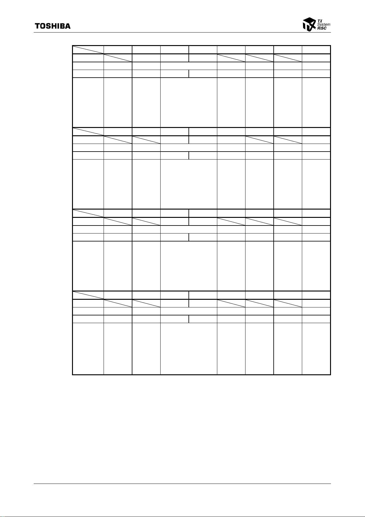
Table 2.1.1 Pin Assignment (144-pin LQFP)
Pin
No.
1 VREFH 37 P11/AD9/A9 73 P90/KEY8/DCLK 109 CVCC
2 VREFL 38 P12/AD10/A10 74 P91/KEY9/PCST2 110 X2
3 P50/AN0 39 P13/AD11/A11 75 P92/TB4OUT/PCST1 111 CVSS
4 P51/AN1 40 P14/AD12/A12 76 P93/TB5OUT/PCST0 112 X1
5 P52/AN2 41 P15/AD13/A13 77 P94/TB6OUT/SDSA0/TPC 113 TEST1
6 P53/AN3 42 P16/AD14/A14 78 P95/TB7IN0/DBGE 114 RESET
7 DAVCC 43 P17/AD15/A15 79 P96/TB7IN1/DINT 115 PD6/XT1
8 DAVSS 44 P20/A0/A16 80 P97/TB7OUT/DRESET 116 PD7/XT2
9 DAREH 45 P21/A1/A17 81 DVCC3 117 NMI
10 DAOUT0 46 P22/A2/A18 82 PA0/TB0IN0/INT3 118 BW0
11 DAOUT1 47 P23/A3/A19 83 PA1/TB0IN1/INT4 119 PB0/TB2IN0/INTB
12 DAOUT2 48 P24/A4/A20 84 PA2/TB0OUT 120 PB1/TB2IN1/INTC
13 P54/AN4 49 P25/A5/A21 85 PA3/TB1IN0/INT5 121 PB2/TB2OUT/TB4IN0
14 P55/AN5 50 P26/A6/A22 86 PA4/TB1IN1/INT6 122 PB3/TB3IN0/INTD
15 P56/AN6 51 P27/A7/A23 87 PA5/TB1OUT 123 PB4/TB3IN1/INTE
16 P57/AN7/ADTRG 52 TEST0 88 PA6/TA1OUT 124 PB5/TB3OUT/TB4IN1
17 P60/AN8/KEY0 53 PLLOFF 89 PA7/TA0IN/KEYA 125 PB6/TA3OUT
18 DVSS 54 DVSS 90 DVSS 126 DVSS
19 P61/AN9/KEY1 55 ALE 91 RSTPUP 127 DVCC3
20 P62/AN10/KEY2 56 DVCC3 92 PC0/TA4IN/INT8 128 PB7/TA2IN/INT7/KEYB
21 P63/AN11/KEY3 57 BW1 93 PC1/TA6IN/INT9 129 PD0/TXD0/TB9IN0
22 P64/AN12/KEY4 58 P30/RD 94 PC2/TA8IN/INTA 130 PD1/RXD0/TB9IN1
23 P65/AN13/KEY5 59 P31/WR 95 PC3/TA5OUT 131 PD2/SCLK0/CTS0
24 P66/AN14/KEY6 60 P32/HWR 96 PC4/TAAIN 132 PD3/TXD1/TBAIN0
25 P67/AN15/KEY7 61 P33/WAIT 97 PC5/TA7OUT 133 PD4/RXD1/TBAIN1
26 DVCC3 62 P34/BUSRQ 98 PC6/TB8IN0/KEYC 134 PD5/SCLK1/CTS1/TABOUT
27 P00/AD0 63 P35/BUSAK 99 PC7/TB8IN1/TA9OUT 135 PE0/TXD3
28 P01/AD1 64 P36/R/W 100 DVCC52 136 PE1/RXD3
29 P02/AD2 65 P37/DSU 101 PF0/TXD5 137 PE2/SCLK3/CTS3
30 P03/AD3 66 DVSS 102 PF1/RXD5/KEYD 138 PE3/TXD4
31 P04/AD4 67 DVCC3 103 PF2/SCLK5/CTS5 139 PE4/RXD4
32 P05/AD5 68 P40/CS0 104 PF3/SCK 140 PE5/SCLK4/CTS4
33 P06/AD6 69 P41/CS1 105 PF4/SO/SDA 141 PE6/INT1/BOOT
34 P07/AD7 70 P42/CS2 106 PF5/SI/SCL 142 PE7/INT2/INTLV
35 DVSS 71 P43/CS3 107 PF6/INT0 143 AVCC
36 P10/AD8/A8 72 P44/SCOUT 108 DVCC51 144 AVSS
Pin Name
Pin
No.
Pin Name
Pin
No.
Pin Name
Pin
No.
Pin Name
TMP1942CY/CZ-6

TX1942CY/CZ
Figure 2.1.2 shows pin assignment for the 177-pin model of the TMP1942.
A1 A2 A3 A4 A5 A6 A7 A8 A9 A10 A11 A12 A13 A14 A15
B1 B2 B3 B4 B5 B6 B7 B8 B9 B10 B11 B12 B13 B14 B15
C1 C2 C3 C4 C5 C6 C7 C8 C9 C10 C11 C12 C13 C14 C15
D1 D2 D3 D4 D5 D6 D7 D8 D9 D10 D11 D12 D13 D14 D15
E1 E2 E3 E4 E12 E13 E14 E15
F1 F2 F3 F4 F12 F13 F14 F15
G1 G2 G3 G4 G12 G13 G14 G15
H1 H2 H3 H4 H12 H13 H14 H15
J1 J2 J3 J4 J12 J13 J14 J15
K1 K2 K3 K4 K12 K13 K14 K15
L1 L2 L3 L4 L12 L13 L14 L15
M1 M2 M3 M4 M5 M6 M7 M8 M9 M10 M11 M12 M13 M14 M15
N1 N2 N3 N4 N5 N6 N7 N8 N9 N10 N11 N12 N13 N14 N15
P1 P2 P3 P4 P5 P6 P7 P8 P9 P10 P11 P12 P13 P14 P15
R1 R2 R3 R4 R5 R6 R7 R8 R9 R10 R11 R12 R13 R14 R15
Figure 2.1.2 177-Pin CSP Pin Assignment
TMP1942CY/CZ-7

TX1942CY/CZ
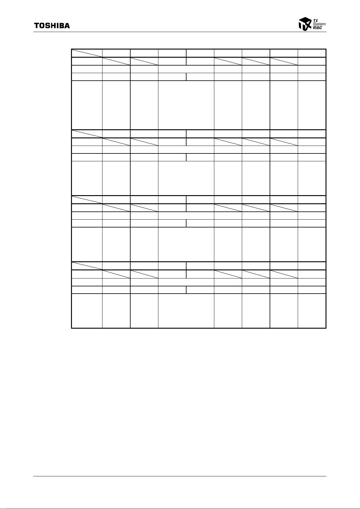
Table 2.1.2 Pin Assignment (177-pin CSP)
Pin
No.
A1 VREFL D1 P50/AN0 H13 NC N4 P16/AD14/A14
A2 AVSS D2 DAVSS H14 NC N5 P21/A1/A17
A3 AVCC D3 P52/AN2 H15 DVSS N6 P25/A5/A21
A4 PE7/INT2/INTLV D4 P51/AN1 J1 P67/AN15/KEY7 N7 DVSS
A5 PE3/TXD4 D5 PE0/TXD3 J2 P65/AN13/KEY5 N8 TEST0
A6 TCK (JTAG) D6 PD3/TXD1/TBAIN0 J3 P66/AN14/KEY6 N9 P30/RD
A7 PD2/SCLK0/CTS0 D7 PB7/TA2IN/INT7/KEYB J4 P64/AN12/KEY4 N10 P32/HWR
A8 PB5/TB3OUT/TB4IN1 D8 DVSS J12 PA6/TA1OUT N11 P37
A9 PB1/TB2IN1/INTC D9 PB2/TB2OUT/TB4IN0 J13 PA7/TA0IN/KEYA N12 DVSS
A10 PD7/TX2 D10 NMI J14 NC N13 P41/CS1
A11 PD6/TX1 D11 NC J15 PA5/TB1OUT N14 P91/KEY9
A12 X1 D12 NC K1 P01/AD1 N15 NC
A13 X2 D13 PF1/RXD5/KEYD K2 DVCC3 P1 NC
A14 CVCC D14 PF3/SCK K3 NC P2 P10/AD8/A8
A15 NC D15 PF6/INT0 K4 NC P3 P12/AD10/A10
B1 NC E1 DAVCC K12 PA2/TB0OUT P4 P20/A0/A16
B2 NC E2 DAOUT0 K13 PA3/TB1IN0/INT5 P5 P22/A2/A18
B3 PE6/INT1 E3 DAREFH K14 PA4/TB1IN1/INT6 P6 P26/A6/A22
B4 PE4/RXD4 E4 P53/AN3 K15 PA1/TB0IN1/INT4 P7 TDO (JTAG)
B5 TRST (JTAG) E5 NC (Bonding not applied) L1 P04/AD4 P8 ALE
B6 PD5/SCLK1/CTS1/TABOUT E12 PC6/TB8IN0/KEYC L2 P02/AD2 P9 BW1
B7 PD0/TXD0/TB9IN0 E13 DVCC52 L3 TMS (JTAG) P10 P33/WAIT
B8 DVCC3 E14 PF0/TXD5 L4 P00/AD0 P11 TDI (JTAG)
B9 PB4/TB3IN1/INTE E15 PF2/SCLK5/CTS5 L12 P97/TB7OUT P12 P40/CS0
B10 PB0/TB2IN0/INTB F1 DAOUT1 L13 DVCC3 P13 P42/CS2
B11 NC F2 P55/AN5 L14 PA0/TB0IN0/INT3 P14 P44/SCOUT
B12 RESET F3 P54/AN4 L15 P96/TB7IN1 P15 NC
B13 CVSS F4 DAOUT2 M1 P07/AD7 R1 P11/AD9/A9
B14 DVCC51 F12 PC2/TA8IN/INTA M2 P05/AD5 R2 NC
B15 NC F13 PC4/TAAIN M3 P03/AD3 R3 NC
C1 VREFH F14 PC5/TA7OUT M4 P14/AD12/A12 R4 P13/AD11/A11
C2 NC F15 PC7/TB8IN1/TA9OUT M5 P15/AD13/A13 R5 P17/AD15/A15
C3 PE5/SCLK4/CTS4 G1 P56/AN6 M6 P24/A4/A20 R6 P23/A3/A19
C4 PE2/SCLK3/CTS3 G2 P61/AN9/KEY1 M7 PLLOFF R7 P27/A7/A23
C5 PE1/RXD3 G3 NC M8 NC R8 NC
C6 PD4/RXD1/TBAIN1 G4 P60/AN8/KEY0 M9 DVCC3 R9 P31/WR
C7 PD1/RXD0/TB9IN1 G12 PC0/TA4IN/INT8 M10 P34/BUSRQ R10 P35/BUSAK
C8 PB6/TA3OUT G13 PC1/TA6IN/INT9 M11 P36/R/W R11 DVCC3
C9 PB3/TB3IN0/INTD G14 NC M12 P93/TB5OUT R12 NC
C10 BW0 G15 PC3/TA5OUT M13 P94/TB6OUT R13 P43/CS3
C11 NC H1 DVSS M14 P95/TB7IN0 R14 NC
C12 TEST1 H2 P63/AN11/KEY3 M15 P92/TB4OUT R15 P90/KEY8
C13 PF4/SO/SDA H3 P57/AN7/ADTRG N1 NC
C14 PF5/SI/SCL H4 P62/AN10/KEY2 N2 DVSS
C15 NC H12 RSTPUP N3 P06/AD6
Pin Name
Pin
No.
Pin Name
Pin
No.
Pin Name
Pin
No.
Pin Name
TMP1942CY/CZ-8
2.2 Pin Usage Information
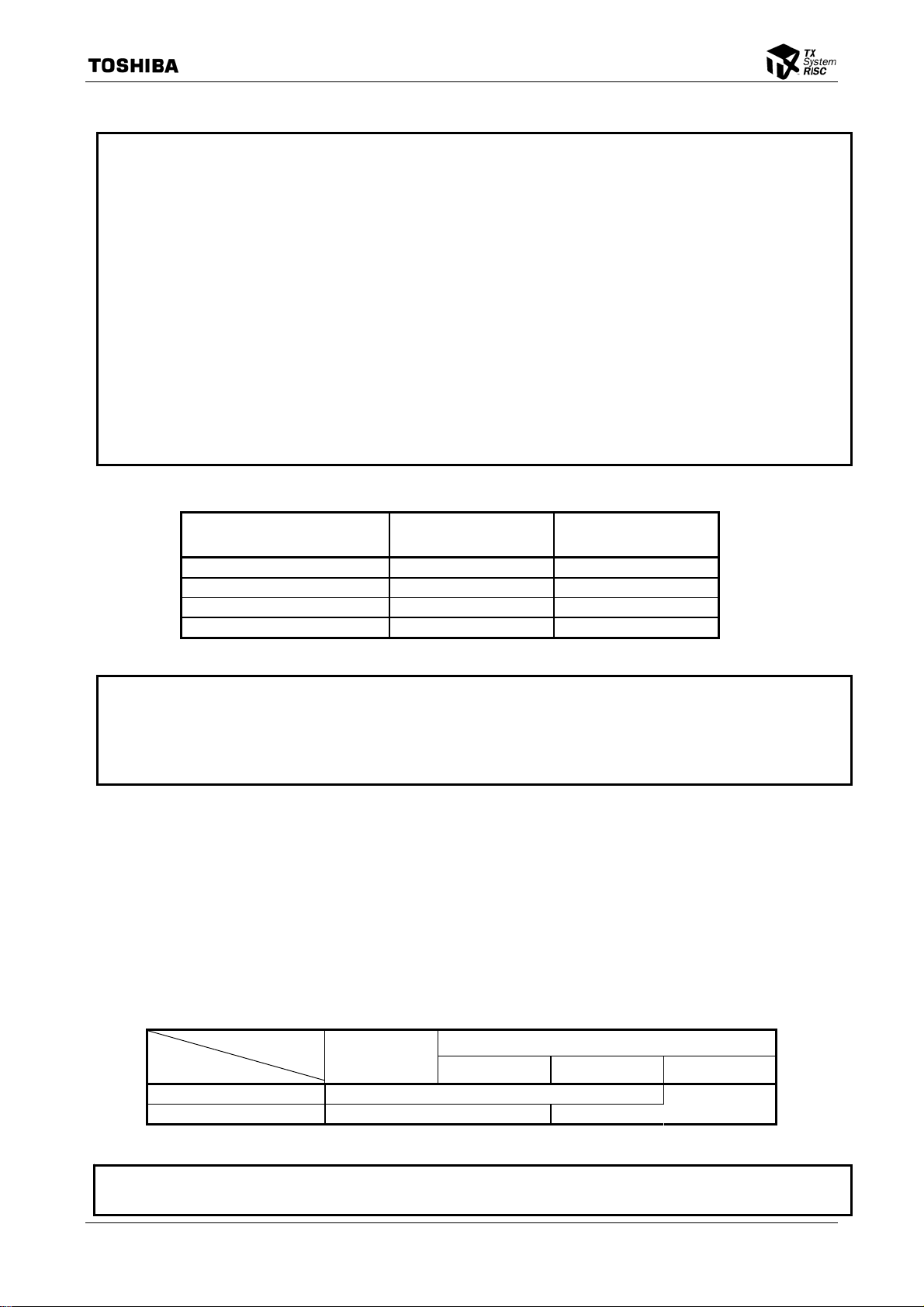
Table 2.2.1 lists the names and functions of the TMP1942’s input/output pins.
Table 2.2.1 Pin Names and Functions
Pin Name # of Pins Type Function
P00~P07
AD0~AD7
P10~P17
AD8~AD15
A8~A15
P20~P27
A0~A7
A16~A23
P30
RD
P31
WR
P32
HWR
P33
WAIT
P34
BUSRQ
P35
BUSAK
P36
R/W
P37
DSU
P40
CS0
P41
CS1
P42
CS2
P43
CS3
P44
SCOUT
P50~P57
AN0~AN7
ADTRG
P60~P67
AN8~AN15
KEY0-KEY7
P90
DSU (DCLK)
KEY8
8 Input/output
Input/output
8 Input/output
Input/output
Output
8 Input/output
Output
Output
1 Output
Output
1 Output
Output
1 Input/output
Output
1 Input/output
Input
1 Input/output
Input
1 Input/output
Output
1 Input/output
Output
1 Input/output
Input
1 Input/output
Output
1 Input/output
Output
1 Input/output
Output
1 Input/output
Output
1 Input/output
Output
8 Input
Input
Input
1 Input/output
Input
Output
1 Input/output
Output
Input
Port 0: Individually programmable as input or output
Address (Lower): Bits 0-7 of the address/data bus
Port 1: Individually programmable as input or output
Address/Data (Upper): Bits 8-15 of the address/data bus
Address: Bits 8-15 of the address bus
Port 2: Individually programmable as input or output
Address: Bits 0-7 of the address bus
Address: Bits 16-23 of the address bus
Port 30: Output-only
Read Strobe: Asserted during a read operation from an external memory device
Port 31: Output-only
Write Strobe: Asserted during a write operation on D0-D7
Port 32: Programmable as input or output (with internal pull-up resister)
Higher Write Strobe: Asserted during a write operation on D8-D15
Port 33: Programmable as input or output (with internal pull-up resister)
Wait: Causes the CPU to suspend external bus activity
Port 34: Programmable as input or output (with internal pull-up resister)
Bus Request: Asserted by an external bus master to request bus mastership
Port 35: Programmable as input or output (with internal pull-up resister)
Bus Acknowledge: Indicates that the CPU has relinquished the bus in response to
Port 36: Programmable as input or output (with internal pull-up resister)
Read/Write: Indicates the direction of data transfer on the bus: 1 = read or dummy
Port 37: Programmable as input or output (with internal pull-up resister)
This pin is used to select the operating mode during reset. The TMP1940CYAF enters
NORMAL mode when this pin is sampled high at the rising edge of
should not be pulled down to a logic 0 during a reset sequence. The TMP1940FDBF,
which has an on-chip flash, uses this pin as an interface to the DSU tool. For details,
refer to Part 4, TMP1940FDBF.
Port 40: Programmable as input or output (with internal pull-up resister)
Chip Select 0: Asserted low to enable external devices at programmed addresses
Port 41: Programmable as input or output (with internal pull-up resister)
Chip Select 1: Asserted low to enable external devices at programmed addresses
Port 42: Programmable as input or output (with internal pull-up resister)
Chip Select 2: Asserted low to enable external devices at programmed addresses
Port 43: Programmable as input or output (with internal pull-up resister)
Chip Select 3: Asserted low to enable external devices at programmed addresses
Port 44: Programmable as input or output
System Clock Output: Drives out a clock signal at the same frequency as the CPU
Port 5: Input-only
Analog input: Input to the A/D converter
External start request for the A/D converter (multiplexed with P57)
Port 6: Input-only
Analog input: Input to the A/D converter
Key on wake-up input (with internal pull-up resister) (dynamic pull-up selectable)
Port 90: Programmable as input or output
DSU pin
Key on wake-up input (with internal pull-up resister) (dynamic pull-up selectable)
BUSRQ
cycle, 0 = write cycle
.
clock (high-speed or low-speed)
TX1942CY/CZ
RESET
. This pin
TMP1942CY/CZ-9

Pin Name # of Pins Type Function
P91
DSU (PCST2)
KEY9
P92
DSU (PCST1)
TB40UT
P93
DSU (PCST0)
TB5OUT
P94
DSU
(SDSA0/TPC)
TB6OUT
P95
DSU (DBGE*)
TB7IN0
P96
DSU (DINT*)
TB7IN1
P97
DSU
(DRESET)
TB7OUT
PA0
TB0IN0
INT3
PA1
TB0IN1
INT4
PA2
TB0OUT
PA3
TB1IN0
INT5
PA4
TB1IN1
INT6
PA5
TB1OUT
PA6
TA1OUT
PA7
TA0IN
KEYA
PB0
TB2IN0
INTB
1 Input/output
Output
Input
1 Input/output
Output
Output
1 Input/output
Output
Output
1 Input/output
Output
Output
1 Input/output
Input
1 Input/output
Input
1 Input/output
Input
Output
1 Input/output
Input
Input
1 Input/output
Input
Input
1 Input/output
Output
1 Input/output
Input
Input
1 Input/output
Input
Input
1 Input/output
Output
1 Input/output
Output
1 Input/output
Input
Input
1 Input/output
Input
Input
Port 91: Programmable as input or output
DSU pin
Key on wake-up input (with internal pull-up resister) (dynamic pull-up selectable)
Port 92: Programmable as input or output
DSU pin
16-Bit Timer 4 Output: Output from 16-bit Timer 4
Port 93: Programmable as input or output
DSU pin
16-Bit Timer 5 Output: Output from 16-bit Timer 5
Port 94: Programmable as input or output
DSU pin
16-Bit Timer 6 Output: Output from 16-bit Timer 6
Port 95: Programmable as input or output
DSU pin
16-Bit Timer 7 Input 0: Count/capture trigger input to 16-bit Timer 7
Port 96: Programmable as input or output
DSU pin
16-Bit Timer 7 Input 1: Capture trigger input to 16-bit Timer 7
Port 97: Programmable as input or output
DSU pin
16-Bit Timer 7 Output: Output from 16-bit Timer 7
Port A0: Programmable as input or output
16-Bit Timer 0 Input 0: Count/capture trigger input to 16-bit Timer 0
Interrupt Request 3: Programmable to be high-level, low-level, rising-edge or
Port A1: Programmable as input or output
16-Bit Timer 0 Input 1: Capture trigger input to 16-bit Timer 0
Interrupt Request 4: Programmable to be high-level, low-level, rising-edge or
Port A2: Programmable as input or output
16-Bit Timer 0 Output: Output from 16-bit Timer 0
Port A3: Programmable as input or output
16-Bit Timer 1 Input 0: Count/capture trigger input to 16-bit Timer 1
Interrupt Request 5: Programmable to be high-level, low-level, rising-edge or
Port A4: Programmable as input or output
16-Bit Timer 1 Input 1: Capture trigger input to 16-bit Timer 1
Interrupt Request 6: Programmable to be high-level, low-level, rising-edge or
Port A5: Programmable as input or output
16-Bit Timer 1 Output: Output from 16-bit Timer 1
Port A6: Programmable as input or output
8-Bit Timer 0/1 Output: Output from 8-bit Timer 0 or 1
Port A7: Programmable as input or output
8-Bit Timer 0 Input: Input to 8-bit Timer 0
Key on wake-up input (with internal pull-up resister) (dynamic pull-up selectable)
Port B0: Programmable as input or output
16-Bit Timer 2 Input 0: Count/capture trigger input/2-phase input pulse counter input to
Interrupt Request B: Programmable to be high-level, low-level, rising-edge or
falling-edge sensitive
falling-edge sensitive
falling-edge sensitive
falling-edge sensitive
16-bit Timer 2
falling-edge sensitive
TX1942CY/CZ
TMP1942CY/CZ-10

Pin Name # of Pins Type Function
PB1
TB2IN1
INTC
PB2
TB2OUT
TB4IN0
PB3
TB3IN0
INTD
PB4
TB3IN1
INTE
PB5
TB3OUT
TB4IN1
PB6
TA3OUT
PB7
TA2IN
INT7
KEYB
PC0
TA4IN
INT8
PC1
TA6IN
INT9
PC2
TA8IN
INTA
PC3
TA5OUT
PC4
TAAIN
PC5
TA7OUT
PC6
TB8IN0
KEYC
PC7
TB8IN1
TA9OUT
PD0
TXD0
TB9IN0
1 Input/output
Input
Input
1 Input/output
Output
Input
1 Input/output
Input
Input
1 Input/output
Input
Input
1 Input/output
Output
Input
1 Input/output
Output
1 Input/output
Input
Input
Input
1 Input/output
Input
Input
1 Input/output
Input
Input
1 Input/output
Input
Input
1 Input/output
Output
1 Input/output
Input
1 Input/output
Output
1 Input/output
Input
Input
1 Input/output
Input
Output
1 Input/output
Output
Input
Port B1: Programmable as input or output
16-Bit Timer 2 Input 1: Capture trigger input/2-phase input pulse counter input to 16-bit
Interrupt Request C: Programmable to be high-level, low-level, rising-edge or
Port B2: Programmable as input or output
16-Bit Timer 2 Output: Output from 16-bit Timer 2
16-Bit Timer 4 Input 0: Count/capture trigger input to 16-bit Timer 4
Port B3: Programmable as input or output
16-Bit Timer 3 Input 0: Count/capture trigger input/2-phase input pulse counter input to
Interrupt Request D: Programmable to be high-level, low-level, rising-edge or
Port B4: Programmable as input or output
16-Bit Timer 3 Input 1: Capture trigger input/2-phase input pulse counter input to 16-bit
Interrupt Request E: Programmable to be high-level, low-level, rising-edge or
Port B5: Programmable as input or output
16-Bit Timer 3 Output: Output from 16-bit Timer 3
16-Bit Timer 4 Input 1: Capture trigger input to 16-bit Timer 4
Port B6: Programmable as input or output
8-Bit Timer 2/3 Output: Output from 8-bit Timer 2 or 3
Port B7: Programmable as input or output
8-Bit Timer 2 Input: Input to 8-bit Timer 2
Interrupt Request 7: Programmable to be high-level, low-level, rising-edge or
Key on wake-up input (with internal pull-up resister) (dynamic pull-up selectable)
Port C0: Programmable as input or output
8-Bit Timer 4 Input: Input to 8-bit Timer 4
Interrupt Request 8: Programmable to be high-level, low-level, rising-edge or
Port C1: Programmable as input or output
8-Bit Timer 6 Input: Input to 8-bit Timer 6
Interrupt Request 9: Programmable to be high-level, low-level, rising-edge or
Port C2: Programmable as input or output
8-Bit Timer 8 Input: Input to 8-bit Timer 8
Interrupt Request A: Programmable to be high-level, low-level, rising-edge or
Port C3: Programmable as input or output
8-Bit Timer 4/5 Output: Output from 8-bit Timer 4 or 5
Port C4: Programmable as input or output
8-Bit Timer A Input: Input to 8-bit Timer A
Port C5: Programmable as input or output
8-Bit Timer 6/7 Output: Output from 8-bit Timer 6 or 7
Port C6: Programmable as input or output
16-Bit Timer 8 Input 0: Count/capture trigger input to 16-bit Timer 8
Key on wake-up input (with internal pull-up resister) (dynamic pull-up selectable)
Port C7: Programmable as input or output
16-Bit Timer 8 Input 1: Capture trigger input to 16-bit Timer 8
8-Bit Timer 8/9 Output: Output from 8-bit Timer 8 or 9
Port D0: Programmable as input or output
Serial Transmit Data 0
Programmable as an open-drain output
16-Bit Timer 9 Input 0: Count/capture trigger input to 16-bit Timer 9
Timer 2
falling-edge sensitive
16-bit Timer 3
falling-edge sensitive
Timer 3
falling-edge sensitive
falling-edge sensitive
falling-edge sensitive
falling-edge sensitive
falling-edge sensitive
TX1942CY/CZ
TMP1942CY/CZ-11
Pin Name # of Pins Type Function
PD1
RXD0
TB9IN1
PD2
SCLK0
CTS0*
PD3
TXD1
TBAIN0
PD4
RXD1
TBAIN1
PD5
SCLK1
CTS1
TABOUT
PD6
XT1
PD7
XT2
PE0
TXD3
PE1
RXD3
PE2
CTS3*
PE3
TXD4
PE4
RXD4
PE5
SCLK4
CTS4
PE6
INT1
BOOT
PE7
INT2
INTLV
PF0
TXD5
1 Input/output
Input
Input
1 Input/output
Input/output
Input
1 Input/output
Output
Input
1 Input/output
Input
Input
1 Input/output
Input/output
Input
Output
1 Input/output
Input
1 Input/output
Output
1 Input/output
Output
1 Input/output
Input
1 Input/output
Input/output
Input
1 Input/output
Output
1 Input/output
Input
1 Input/output
Input/output
Input
1 Input/output
Input
1 Input/output
Input
1 Input/output
Output
Port D1: Programmable as input or output
Serial Receive Data 0
16-Bit Timer 9 Input 1: Capture trigger input to 16-bit Timer 9
Port D2: Programmable as input or output
Serial Clock Input/Output 0
Serial Clear-to-Send 0
Programmable as an open-drain output
Port D3: Programmable as input or output
Serial Transmit Data 1
Programmable as an open-drain output
16-Bit Timer A Input 0: Count/capture trigger input to 16-bit Timer A
Port D4: Programmable as input or output
Serial Receive Data 1
16-Bit Timer A Input 1: Capture trigger input to 16-bit Timer A
Port D5: Programmable as input or output
Serial Clock Input/Output 1
Serial Clear-to-Send 1
Programmable as an open-drain output
8-Bit Timer A/B Output: Output from 8-bit Timer A or B
Port D6: Programmable as input or open-drain output
Connection pin for a low-speed crystal
Port D7: Programmable as input or open-drain output
Connection pin for a low-speed crystal
Port E0: Programmable as input or output
Serial Transmit Data 3
Programmable as an open-drain output
Port E1: Programmable as input or output
Serial Receive Data 3
Port E2: Programmable as input or output
Serial Clock Input/Output 3
Serial Clear-to-Send 3
Programmable as an open-drain output
Port E3: Programmable as input or output
Serial Transmit Data 4
Programmable as an open-drain output
Port E4: Programmable as input or output
Serial Receive Data 4
Port E5: Programmable as input or output
Serial Clock Input/Output 4
Serial Clear-to-Send 4
Programmable as an open-drain output
Port E6: Programmable as input or output
Interrupt request 1: Individually programmable to be high-level, low-level,
Single-boot mode setting pin: Used when rewriting built-in flash memory (low active).
Port E7: Programmable as input or output
Interrupt request 2: Individually programmable to be high-level, low-level,
Interleave mode setting pin: This pin should be pulled up when using interleave mode.
Port F0: Programmable as input or output
Serial Transmit Data 5
Programmable as an open-drain output
rising-edge or falling-edge sensitive.
During normal operation, this pin should be pulled up.
This pin should always be pulled up for the mask ROM
version.
rising-edge or falling-edge sensitive.
Otherwise, it should be pulled down.
TX1942CY/CZ
TMP1942CY/CZ-12
TX1942CY/CZ
Pin Name # of Pins Type Function
PF1
RXD5
KEYD
PF2
SCLK5
CTS5
PF3
SCK
PF4
SO
SDA
PF5
SI
SCL
PF6
INT0
ALE 1 Output Address Latch Enable
TEST0 1 Input Test pin
TEST1 1 Input Test pin
RSTPUP 1 Input When this pin is driven high (upon reset), pull-up for ports 3 and 4 is enabled. When this
DAOUT0-2 3 Output D/A converter output
NMI 1 Input Non-maskable Interrupt Request: Causes an NMI interrupt on the falling edge
BW0~1 2 Input Set both AM0 and AM1 to 1.
PLLOFF 1 Input This pin should be tied to logic 1 when the frequency multiplied clock from the PLL is
RESET 1 Input Reset (with internal pull-up resister): Initializes the whole TMP1940CYAF
VREFH 1 Input Input pin for high reference voltage for the A/D converter.
VREFL 1 Input Input pin for low reference voltage for the A/D converter.
AVCC 1 ⎯ Power supply pin for the A/D converter. This pin should always be connected to power
AVSS 1 ⎯ Ground pin for the A/D converter. This pin should always be connected to ground even
DAVCC 1 ⎯ Power supply pin for the D/A converter. This pin should always be connected to power
DAVSS 1 ⎯ Ground pin for the D/A converter. This pin should always be connected to ground even
DAREFH 1 ⎯ Reference voltage input pin for the D/A converter
X1/X2 2 Input/output Resonator connecting pin
CVCC 1 ⎯ Power supply pin for the oscillator
CVSS 1 ⎯ Ground pin for the oscillator (0 V)
DVCC3 4 ⎯ Power supply pins
DVCC51 1 ⎯ Power supply pin (port F)
DVCC52 1 ⎯ Power supply pin (port C)
DVSS 5 ⎯ Ground pins (0 V)
Port C becomes a 5 V port when a 5 V power supply is connected to DVCC52.
Port F becomes a 5 V port when a 5 V power supply is connected to DVCC51.
1 Input/output
Input
Input
1 Input/output
Input/output
Input
1 Input/output
Input/output
1 Input/output
Output
Input/output
1 Input/output
Input
Input/output
Input/output
Input
Port F1: Programmable as input or output
Serial Receive Data 5
Key on wake-up input (with internal pull-up resister) (dynamic pull-up selectable)
Port F2: Programmable as input or output
Serial Clock Input/Output 5
Serial Clear-to-Send 5
Programmable as an open-drain output
Port F3: Programmable as input or output
Clock input/output pin when the serial bus interface is in SIO mode
Port F4: Programmable as input or output
Data transmission pin when the serial bus interface is in SIO mode
Data transmission/reception pin when the serial bus interface is in I
Programmable as an open-drain output
Port F5: Programmable as input or output
Data reception pin when the serial bus interface is in SIO mode
Clock input/output pin when the serial bus interface is in I
Programmable as an open-drain output
Port F6: Programmable as input or output
Interrupt request 0: Individually programmable to be high-level, low-level, rising-edge or
(This signal is driven out only when external memory is accessed)
pin is driven low, pull-up is disabled.
used; otherwise, it should be tied to logic 0.
supply even when the A/D converter is not used.
when the A/D converter is not used.
supply even when the D/A converter is not used.
when the D/A converter is not used.
falling-edge sensitive.
2
C mode
2
C mode
Note: When the DSU is enabled, port 9 functions as the processor probe interfacing signal
regardless of the setting of the port 9 control register (P9CR).
TMP1942CY/CZ-13

The following table lists the JT AG specific pins added to the CSP package:
Pin Name # of Pins Type Function
TRST 1 Input JTAG reset pin (with internal pull-up resistor)
TCK 1 Input JTAG clock pin (with internal pull-up resistor)
TDI 1 Input JTAG data input pin (with internal pull-up resistor)
TDO 1 Output JTAG data outpu t pin
TMS 1 Input JTAG mode switching input pin (with internal pull-up resistor)
TX1942CY/CZ
TMP1942CY/CZ-14

3. Functional Description
This section describes the functions and basic operation of each indivi dual circuit bloc k i n the TMP1942 se ries
devices.
3.1 Processor Core
The TX1942 contains a high-performance 32-bit processor core (the TX19 pro cessor core). For details of
the operation of the processor core, refer to “TX19 Family Architecture”.
Functions unique to the TMP1942, which are not explained in “TX19 Family Architecture”, are described
below.
Recommended power-on sequence:
In powering up this device, it is recommended that the DVCC3 be turned on first.
At power-on, the pull-up resistors and input & output buffers pull-down resistors attached to
the I/O ports of the 5V supply domain may rail become unstable or a through current may pass
through the port until the DVCC3 has stabilized, when an injection order is not kept.
TMP1942CY/CZ
3.1.1 Reset Operation
To reset the TMP1942,
power supply voltage is within the rated operating range and the internal high-frequency oscillator is
oscillating stably. (With the device operating at 32 MHz, this period is equal to 3 μs if the PLL is being
used and 6 μs if the PLL is not being used.) After a reset the PLL-multiplied clock is specified by the
setting of the
To reset the TMP1942,
supply voltage and the internal high-frequency oscillator have stabilized. This time is typically 3 μs at 32
MHz when the on-chip PLL is utilized, and 6μs otherwise. After a reset, either the PLL-multiplied clock
or an external clock is selected, depending on the logi c state of the
clock is geared down to 1/8 for internal operation.
The following occurs as a result of a reset:
• The System control coprocessor (CP0) registers within the TX19 core processor are initialized.
• The Reset exception is taken. Program control is transferred to the exception handler at a
RESET
PLLOFF pin and the clock gear is initialized to 1/8 mode.
RESET
For details, refer to the Architecture manual.
predefined address. This predefined location is called an exception vector, which directly
indicates the start of the actual exception handler routine. The Reset exception is always
vectored to virtual address 0xBFC0_0000 (which is the same as f or t he N onmaskable Interrupt
exception).
must be input Low (at 0) for at least 12 system clock cycles while the
must be asserted for at least 12 system clock periods after the power
PLLOFF
pin. By default, the selected
• All on-chip I/O peripheral registers are initialized.
• All port pins, including those multiplexed with on-chip peripheral functions, are configured as
either general-purpose inputs or general-purpose outputs.
TMP1942CY/CZ-15
3.2 Memory Map
Figure 3.2.1 shows a memory map of the TMP1942.
0xFFFF_FFFF
0xFF00_0000
0xC000_0000
0xBFC0_0000
0xA000_0000
0x8000_0000
0x0007_FFFF
0x0000_0000
Virtual address
16 Mbytes reserved
16 Mbytes reserved
Kseg2
(cacheable)
Kseg1
(uncacheable)
Kseg0
(cacheable)
Kuseg
(cacheable)
Physical address
16 Mbytes reserved
Kseg2
(1 Gbyte)
16 Mbytes reserved
Kuseg
(2Gbyte)
Internal ROM area
reflected
Cannot be accessed
Internal ROM
512 Mbytes
0x4003_FFFF
0x4000_0000
0x1FC3_FFFF
0x1FC0_0000
TMP1942CY/CZ
Internal I/O
(Reserved)
Internal RAM (16KB)
(Reserved)
Reserved for
debugging (2 MB)
(Reserved)
User program area
Maskable interrupt
area
Exception vector area
0xFFFF_E000
0xFFFF_AFFF
0xFFFF_7000
0xFF3F_FFFF
0xFF20_0000
0xFF00_0000
0x1FC3_FFFF
0x1FC0_0400
0x1FC0_0000
Figure 3.2.1 Memory Map
Note 1: The internal ROM is mapped into the memory space from 0x1FC0_0000 to 0x1FC3_FFFF (for a 256-KB ROM) or
0x1FC0_0000 to 0x1FC5_FFFF (for a 384-KB ROM). The internal RAM is mapped into the memory space from
0xFFFF_8000 to 0xFFFF_BFFF (for a 16-KB RAM).
Note 2: The memory space from 0xFFFF_4000 to 0xFFFF_BFFF is a reserved RAM area. Any area other than those shown above,
where physical memory is located, should not be accessed.
Note 3: The internal memory data is stored in contiguous physical address locations starting at 0x1FC0_0000.
If exception vector addresses are placed in internal ROM, the system control coprocessor (CP0) Status register's BEV bit
must be set to 1 (the default). (This is because exception vector addresses are dispersed if BEV = 0.) If memory is added
externally, the BEV bit can be set to 0.
However, since a virtual address space of 0x0000_0000 ±32 KB is easier to access for reasons of code efficiency, this area
is reflected in the contiguous physical address space from 0x4000_0000 upwards (as indicated by the shaded area) which
corresponds to a virtual address space starting at 0x0000_0000 and which is equal in size to the internal memory. Hence,
accessing this area is equivalent to accessing the internal memory.
Example: Using 32-bit ISA
• Access to the 0x0000_0000 ±32 KB area
ADDIU r2, r0, 7 ; r 2 ← (0x0000_0007)
SW r2, Io (_t) (r0) ; 0x0000_xxxx ← (r2)
↑
Can be accessed using a single instruction.
• Access to areas other than 0x0000_0000 ±32 KB
LUI r3, hi (_f) ; ← Upper address is set to r3.
ADDIU r2, r0, 8 ; r2 ← (0x0000_0008)
SW r2, Io (_f) (r3) ; Memory is accessed after lower address has been set.
Note 4: The TX1942 supports access to only 16 Mbytes of physical space as external address space. A 16-Mbyte physical address
space can be placed in any chip-select area within the CPU's 3.5 Gbytes of physical address space.
However, when access to the internal memory, internal I/O space or a reserved area is performed, the external address
space cannot be accessed simultaneously, since the other t ypes of access have priority.
Note 5: Do not place an instruction in the last four words of the physical area.
• The relevant area of the internal ROM is 0x1FC3_FFF0 to 0x1FC3_FFFF (for a 256-KB ROM) or 0x1FC5_FFF0 to
0x1FC5_FFFF (for a 384-KB ROM).
• If ROM is added externally, this restriction applies to the last four words of the installed memory
(system-dependent).
TMP1942CY/CZ-16
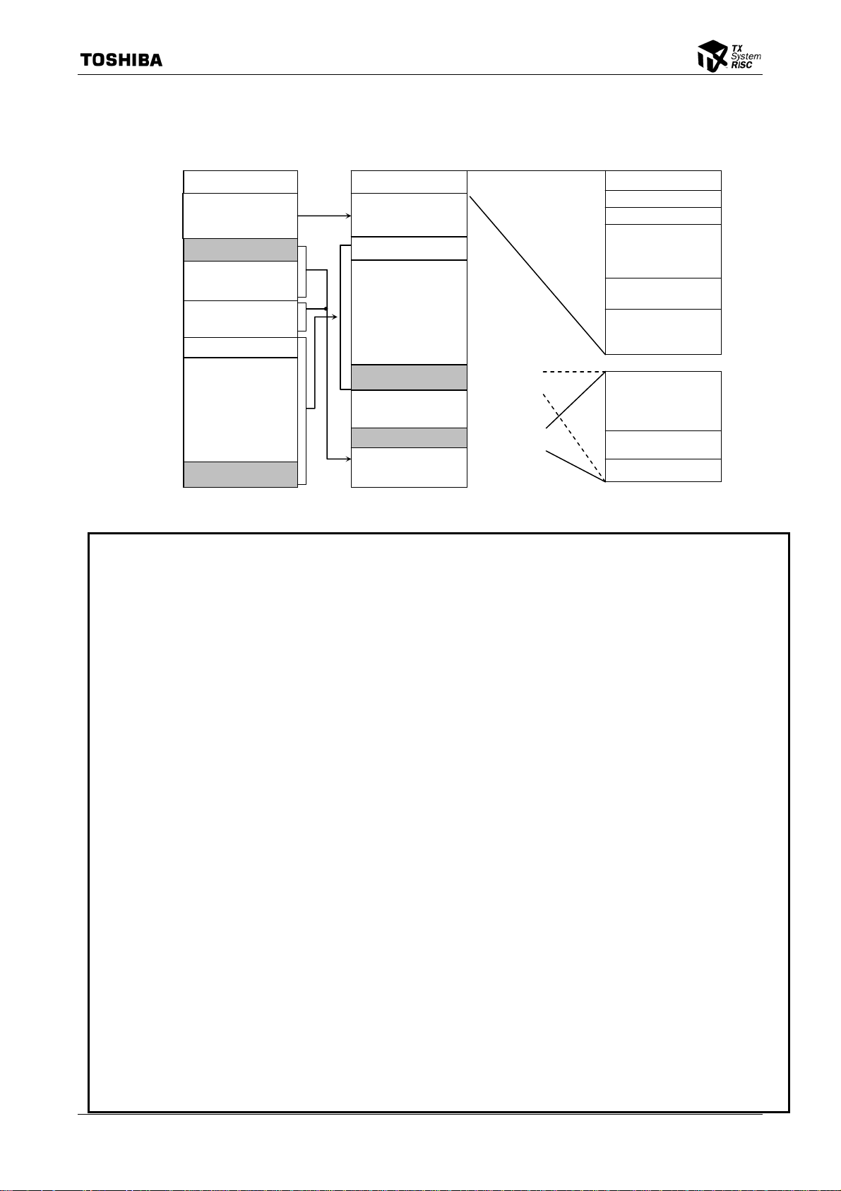
3.3 Clock/Standby Control
There are essentially two modes of clock operation: single-clock mode (which uses only the X1 and X2
pins) and dual-clock mode (which uses the X1 and X2 pins as well as the XT1 and XT2 pins).
Figure 3.3.1 shows the state transition dia
(I/O select operation)
SLEEP mode (fc only)
IDLE mode
(CPU halted)
(I/O select operation)
IDLE mode
(CPU halted)
(only real-time clock
timer operating)
Instruction
Instruction
gram for each operation mode.
Reset
Reset terminated
Instruction
Interrupt
NORMAL mode
(fc/gear value)
(a) State transition in single-clock mode
Reset
Reset terminated
NORMAL mode
Interrupt
Interrupt
Instruction
Interrupt
(fc/gear value)
Instruction
SLOW mode
(fs)
Interrupt
Instruction
Interrupt
TMP1942CY/CZ
Instruction
Interrupt
Instruction
STOP mode
(all circuits turned off)
STOP mode
(all circuits turned off)
Note 1: Before transition to SLOW/SLEEP mode can occur, the low-speed oscillator (fs) must be oscillating stably.
Note 2: When SLEEP mode is terminated, the device returns to the state in which it was placed before entering SLEEP mode.
Note 3: The state to which the device returns when STOP mode is terminated can be specified using system control register
SYSCR0.
(b) State transition in dual-clock mode
Figure 3.3.1 State Transition Diagrams for Different Modes
Reset
Reset terminated
PLLOFF pin (High)
PLL clock used
NORMAL mode
fc = fpll = fosc × 4
fsys = fc/8
∴fsys = fosc/2
fperiph = fsys
Reset
Reset terminated
PLLOFF pin (Low)
PLL not used
NORMAL mode
fc = fosc/2
fsys = fc/8
∴fsys = fosc/16
fperiph = fsys
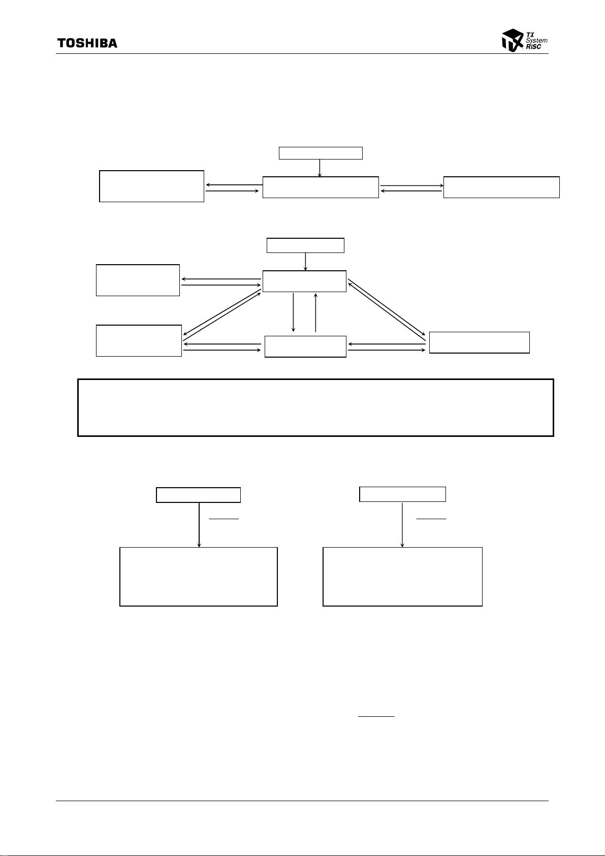
A. When a clock generated by the PLL is used
B. When the PLL is not used
Figure 3.3.32 Default States When the PLL is Used and Those When the PLL is Not Used
fosc: Clock frequency input via X1 and X2 pins
fs: Clock frequency input via XT1 and XT2 pins
fpll: Clock frequency multiplied (x4) by PLL
fc: Clock frequency selected by setting of
PLLOFF pin
fgear: Clock frequency selected by SYSCR1<GEAR1:GEAR0>
System clock fsys: Clock frequency selected by SYSCR1<SYSCK>
fperiph: Input clock for peripheral I/O prescaler
TMP1942CY/CZ-17

3.3.1 Block Diagram of Clock Circuits
1. Main system clock
• A crystal can be connected between X1 and X2, or X1 can be externally driven with a clock.
•
PLLOFF The on-chip PLL can be enabled or disabled (bypassed) during reset by using the
PLLOFF pin. When the PLL is enabled, the input clock frequency is multiplied by four.
• The clock gear can be programmed t o divide the clock by 2, 4 or 8. (The default is 1/8 on reset.)
• Input clock frequency
Input Frequency Range fmax fmin
PLLON
(for both resonator and external input)
Resonator 16~20 (MHz) 20 MHz 1 MHz
PLLOFF
*1. SYSCR1<DFOSC> must be 0. The default is 0.
2. Sub-system clock
• Generated using a 32.768-kHz resonator (external input also accepted).
• SLOW mode: The CPU runs at low speed.
External input
TMP1942CY/CZ
5~8 (MHz) 32 MHz 2.5 MHz
16~20 (MHz) 20 MHz 1 MHz
20
∼32 (MHz) 16 MHz
*1
1.25 MHz
• SLEEP mode: Only the timer for real-time clock, 2-phase pulse inp ut counter, and dynamic
pull-up operate.
TMP1942CY/CZ-18
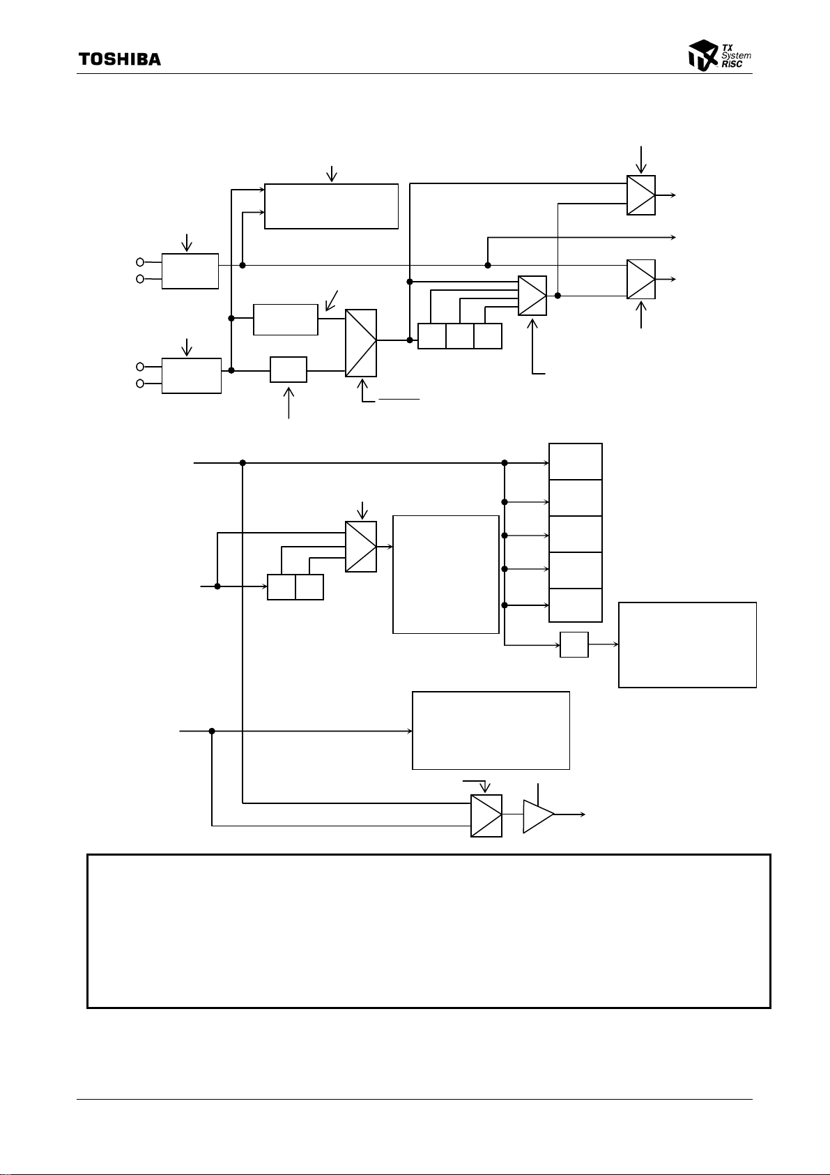
3. Block di ag ram
SYSCR0
<XTEN>
XT1
XT2
Low-speed
oscillator
SYSCR0
<XEN>
X1
X2
High-speed
oscillator
fsys
fperiph
fs
SYSCR0<WUEF>
SYSCR2<WUPT1 : 0>
SYSCR3<LUPTM>
Warm-up timer
Lock-up (PLL) timer
fs
Fpll
PLL
÷2
fosc
SYSCR1 <DFOSC>
÷2 ÷4
= fosch × 4
Selector
SYSCR0
<PRCK1:0>
SYSCR3 <SCOSEL>
fc
÷2 ÷4 ÷8
PLLOFF (default pin setting)
Peripheral I/O
(prescaler input)
TMRA/B, SIO
SBI, ADC
Timer for real-time clock
2-phase pulse input counter
KWUP
TMP1942CY/CZ
SYSCR1 <FPSEL>
fgear
SYSCR1 <SYSCK>
SYSCR1 <GEAR1:0>
Divide by 8 after reset
CPU
ROM
RAM
DMAC
INTC
Peripheral I/O
÷2
ADC,DA,TMRA/B,
SIO,SBI,PIO, WDT, RTC
SCOUT
fperiph
(to peripheral I/O)
fs
fsys
Note 1: When using the clock gear to reduce the system clock frequency, make sure that φTn of the
prescaler output for each peripheral I/O block satisfies the following relationship:
φTn<fsys/2
To this end, set the clock-related registe rs so that φTn is slower than fsys/2.
When selecting a low-speed system clock (fs), only the timer for real-time clock, 2 -phase pulse input
counter, and dynamic pull-up can operate.
Figure 3.3.3 Block Diagram of Dual-Clock and Standby Functions
TMP1942CY/CZ-19
TMP1942CY/CZ
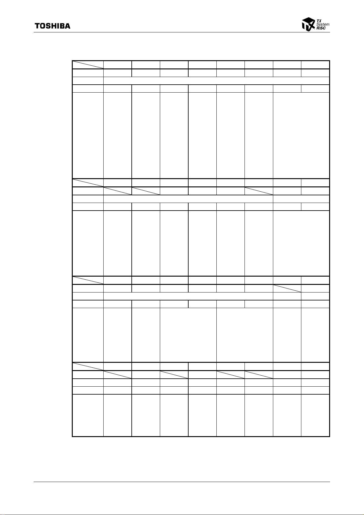
3.3.2 Clock Generator (CG) Registers
(1) Clock-related registers
SYSCR0 Bit Symbol XEN XTEN RXEN RXTEN RSYSCK WUEF PRCK1 PRCK0
(0xFFFF_EE00) Read/Write R/W
After reset 1 0 1 0 0 0 0 0
Function High-speed
SYSCR1 Bit Symbol SYSCK FPSEL DFOSC GEAR1 GEAR0
(0xFFFF_EE01) Read/Write R/W R/W
After reset - - 0 0 0 - 1 1
Function System
SYSCR2 Bit Symbol DRVOSCH DRVOSCL WUPT1 WUPT0 STBY1 STBY0 DRVE
(0xFFFF_EE02) Read/Write R/W - R/W
After reset 0 0 1 0 1 1 - 0
Function High-speed
SYSCR3 Bit Symbol SCOSEL ALESEL LUPFG LUPTM
(0xFFFF_EE03) Read/Write - R/W - R/W - - R R/W
After reset - 0 - 1 - - 0 0
Function SCOUT
7 6 5 4 3 2 1 0
oscillator
0: Turned off
1: Oscillating
Low-speed
oscillator
0: Turned off
1: Oscillating
High-speed
oscillator
after exit
from STOP
mode
0: Turned off
1: Oscillating
Low-speed
oscillator
after exit
from STOP
mode
0: Turned off
1: Oscillating
Clock
selection
after exit
from STOP
mode
0: High speed
1: Low speed
Oscillator
warm-up
timer (WUP)
control
Write 0:
Don't care
Write 1:
WUP start
Read 0:
WUP finished
Read 1:
WUP
operating
Prescaler clock selection
00: fperiph/4
01: fperiph/2
10: fperiph
11: (reserved)
15 14 13 12 11 10 9 8
clock
selection
0: High speed
(fc)
1: Low speed
(fs)
fperiph
selection
0: fgear
1: fc
High-speed
oscillator
frequency
division
selection
0: Divide by 2
1: Divide by 1
High-speed clock (fc)
gear selection
00: fc
01: fc/2
10: fc/4
11: fc/8
23 22 21 20 19 18 17 16
Standby mode selection
00: Reserved
01: STOP mode
10: SLEEP mode
11: IDLE mode
1: Pins are
also
driven in
STOP
mode.
oscillator
driving
capability
control
0: Normal
1: Weak
Low-speed
oscillator
driving
capability
control
0: Normal
1: Weak
Oscillator warm-up time
selection
2
/input frequency
00: 2
8
/input frequency
01: 2
10: 214/input frequency
11: 216/input frequency
31 30 29 28 27 26 25 24
output
selection
0: fs
1: fsys
ALE output
Lock-up flag
width
selection
0: fsys × 0.5
1: fsys × 1.5
0: LUP
finished
1: LUP in
operation
Lock-up time
selection
16
0: 2
/input
frequency
12
/input
1: 2
frequency
TMP1942CY/CZ-20

TMP1942CY/CZ
Note 1: Standby mode selection depends on the settings of the Doze and Halt bits in the CP0's internal
Config register. If the Halt bit = 1, the device will enter the mode selected by STBY[1:0].
If the Doze bit = 1, the device will always enter IDLE mode.
Note 2: When the PLL is not used, set the LUPTM bit in the SYSCR3 register to 1 (i.e., select 2
frequency).
Note3: The WURT1-WUPT0 bitys in the SYSCR2 must be not be changed during the oscillator warm-up
event ( e.g. SLEEP-NORMAL-SLEEP)
Note 4: Do as follows to change the operating mode immediately after the device has warmed up from the
clock stop state (e.g., from SLEEP mode to NORMAL mode to SLEEP mode).
• Warming up by hardware
(1) Moving from STOP or SLEEP mode to NORMAL mode
1) When the PLL is used
Before moving to the next operating mode, ensure that the lock-up bit, LUPFG, in the SYSCR3
register has been cleared to zero and wait for five or more instructions to complete (including the
instruction to check the LUPFG flag).
2) When the PLL is not used
• When the oscillator warm-up time (SYSCR2<WUPT1:0>) is programmed as “01” (i.e., 2
Before moving to the next operating mode, ensure that the lock-up bit, LUPFG, in the SYSCR3 register has
been cleared to zero and wait for five or more instructions to complete.
• When the oscillator warm-up time (SYSCR2<WUPT1:0>) is programmed as “10” (214/input frequency) or
“11” (216/input frequency). Before moving to the next operating mode, wait for five or more instructions to
complete.
8
/input frequency).
12
/input
(2) Moving from STOP or SLEEP mode to SLOW mode
It is possible to move to SLOW mode immediately after the device has warmed up from STOP or SLEEP
mode.
• Warming up by software
(1) Moving from SLOW mode to NORMAL mode
1) When the PLL is used
It is possible to move to NORMAL mode immediately after the device has warmed up. However, to
move to another mode after that, ensure that the lock-up bit, LUPFG , in the SYSCR3 register has been
cleared to zero and wait for five or more instructions to complete (including the instruction to check the
LUPFG flag).
2) When the PLL is not used
• When the oscillator warm-up time (SYSCR2<WUPT1:0>) is programmed as “01” (i.e., 2
It is possible to move to NORMAL mode immediately after the d evice has warmed up . However, to move to
another mode after that, ensure that the lock-up bit, LUPFG, in the SYSCR3 register has been cleare d to zero
and wait for five or more instructions to complete.
8
/input frequency).
• When the oscillator warm-up time (SYSCR2<WUPT1:0>) is programmed as “10” (214/input
frequency) or “11” (2
16
/input frequency). It is possible to move to NORMAL mode immediately
after the device has warmed up. However, to move to another mode after that, wait for five or
more instructions to complete.
(2) Moving from NORMAL mode to SLOW mode
Before moving to SLOW mode, ensure that the warm-up end flag (i.e., the WUEF bit in the SYSCR0
register) is cleared and wait for five or more instructions to complete.
TMP1942CY/CZ-21
TMP1942CY/CZ
(2) Standby (STOP/SLEEP mode) termination interrupts
IMCGA0
(0xFFFF_EE10) Read/Write ⎯ ⎯ R/W ⎯ ⎯ ⎯ R/W
After reset ⎯ ⎯ 1 0 ⎯ ⎯ ⎯ 0
Function Active state setting for
Bit Symbol
Read/Write ⎯ ⎯ R/W ⎯ ⎯ ⎯ R/W
After reset ⎯ ⎯ 1 0 ⎯ ⎯ ⎯ 0
Function Active state setting for
Bit Symbol EMCG21 EMCG20
Read/Write ⎯ ⎯ R/W ⎯ ⎯ ⎯ R/W
After reset ⎯ ⎯ 1 0 ⎯ ⎯ ⎯ 0
Function Active state setting for
Bit Symbol EMCG31 EMCG30 INT3EN
Read/Write ⎯ ⎯ R/W ⎯ ⎯ ⎯ R/W
After reset ⎯ ⎯ 1 0 ⎯ ⎯ ⎯ 0
Bit Symbol EMCG01 EMCG00 INT0EN
Function Active state setting for
7 6 5 4 3 2 1 0
INT0
INT0 standby termination
request
00: Low level
01: High level
10: Falling edge
11: Rising edge
request
input
0: Disable
1: Enable
15 14 13 12 11 10 9 8
EMCG11 EMCG10 DFOSC INT1EN
INT1 standby termination
request
00: Low level
01: High level
10: Falling edge
11: Rising edge
INT1
request
input
0: Disable
1: Enable
23 22 21 20 19 18 17 16
INT2
INT2 standby termination
request
00: Low level
01: High level
10: Falling edge
11: Rising edge
INT2EN
request
input
0: Disable
1: Enable
31 30 29 28 27 26 25 24
INT3 standby termination
request
00: Low level
01: High level
10: Falling edge
11: Rising edge
INT3
request
input
0: Disable
1: Enable
TMP1942CY/CZ-22
TMP1942CY/CZ
IMCGB0
(0xFFFF_EE14) Read/Write ⎯ ⎯ R/W ⎯ ⎯ ⎯ R/W
After reset
Function
Bit Symbol EMCG51 EMCG50 KWUPEN
Read/Write ⎯ ⎯ R/W ⎯ ⎯ ⎯ R/W
After reset ⎯ ⎯ 1 0 ⎯ ⎯ ⎯ 0
Function These bits should always
Bit Symbol
Read/Write ⎯ ⎯ R/W ⎯ ⎯ ⎯ R/W
After reset ⎯ ⎯ 1 0 ⎯ ⎯ ⎯ 0
Function These bits should always
Bit Symbol EMCG71 EMCG70
Read/Write ⎯ ⎯
After reset
Function
Bit Symbol
7 6 5 4 3 2 1 0
EMCG41 EMCG40 INT4EN
⎯ ⎯ 1 0 ⎯ ⎯ ⎯ 0
Active state setting for
INT4 standby termination
request
00: Low level
01: High level
10: Falling edge
11: Rising edge
INT4
request
input
0: Disable
1: Enable
15 14 13 12 11 10 9 8
be set to 01.
KWUP
request
input
0: Disable
1: Enable
23 22 21 20 19 18 17 16
EMCG61 EMCG60
INTBCDE
be set to 01.
INTBCDEEN
request
input
0: Disable
1: Enable
31 30 29 28 27 26 25 24
INTRTCEN
R/W
0
request
input
0: Disable
1: Enable
⎯ ⎯
R/W
1 0
These bits should always
be set to 11.
⎯ ⎯ ⎯
⎯ ⎯ ⎯
INTRTCEN
TMP1942CY/CZ-23

Note 1: When enabling an interrupt source as a means of terminating a standby mode, always set the active
state for the corresponding interrupt request.
Note 2: When using an interrupt, always perform the following steps in order:
(1) Enable the input for the interrupt if the corresponding pin is also used for a ge neral-purpose
port or any other purpose.
(2) Set the active state for the interrupt during initialization.
(3) Clear the interrupt request.
(4) Enable the interrupt.
Note 3: The TMP1942 has eight interrupt sources (INT0~INT4, INTRTC, INTB/INTC/INTD/INTE, and
KWUP0-KWUPD) which can be used as a means of terminating a standby mode. For INT0 to INT4,
use the CG block to specify whether they are used to terminate a st andby mode and to spe cify their
active edge or level. For INTB/INTC/INTD/INTE and KWUP0-KWUPD, use the CG block to specify
whether they are used to terminate a standby mode and use INTBCDEST and KWUPSTn,
respectively , to specify their active edge or level. Set the active stat e for the corresponding interrupt
source to High in the INTC block.
Example: Enable the INT0 interrupt
IMCGA0<EMCG01:00> = “10” CG block
IMCGA0<INT0EN> = “1” (Input is enabled on the falling edge.)
IMC0L<EIM11:10> = “01” INTC block
IMC0L<IL12:10> = “101” (A High-level interrupt is active and the interrupt level is 5.)
All interrupt sources other than those which are used to terminate S TOP/SLEEP mode are set in the
INTC circuit block.
TMP1942CY/CZ
Note 4: Among the above eight interrupt sources used to request the termination of a standby mode, INT0
to INT4 do not require settings in the CG block if they are used as normal interrupts. They still,
however, require level or edge spe cification in the INTC. If INTB/INTC/INTD/INTE and
KWUP0-KWUPD are used as normal interrupts, specify the active level or edge using
INTBCDEST/KWUPSTn and specify the High level in the INTC. Settings in the CG are not required.
INTRTC always requires settings in both the CG and INTC even if it is used as a normal interrupt.
All interrupt sources other than those which are used to terminate a standby mod e are set in the
INTC circuit block.
TMP1942CY/CZ-24

TMP1942CY/CZ
(3) Interrupt request clear register
EICRCG
(0xFFFF_EE20) Read/Write ⎯ ⎯ ⎯ ⎯ ⎯ W
After reset
Function
Bit Symbol
7 6 5 4 3 2 1 0
ICRCG2 ICRCG1 ICRCG0
⎯ ⎯
Clear interrupt request
1 0
⎯ ⎯ ⎯ ⎯
000: INT0 100: INT4
001: INT1 101:KWUP
010: INT2 110: INTB/C/D/E
011: INT3 111: INTRTC
Note : To clear any of the eight interrupt sources which are used for terminating a standby mode:
(1) For KWUP, use KWUPCLR.
(2) For extended interrupts INTB/INTC/INTD/INTE, use INTFLG.
(3) For INT0 to INT4 and INTRTC, perform the clea ring operation twice, first in the CG block and
then in the INTC block.
(4) For all other interrupt sources, use the INTC block.
3.3.3 System clock control unit
When reset, the device enters single-clock mode with the result that XEN = 1, XTEN = 0 and
GEAR1:0 = 11 ; the system clock fsys is set to fc/8 (= fc × 1/8). (Since the PLL multiplies the original
oscillation frequency by 4, fc equals to fosc × 4, where fosc is the original oscillation frequency.) For
example, if the X1 and X2 pins are connected to an 8-MHz resonator, a reset will set fsys to 4 MHz (= 8
MHz × 4 × 1/8).
To disable the system from using a PLL-multiplied clock as the system clock by default, drive the
PLLOFF pin Low. In this case, too, the system clock fsys will be set to fc/8 (= fc × 1/8) by a reset.
However, since SYSCR1<DFOSC> is initialized to 0 by a reset (so that fc = fosc × 1/2), if the X1 and X2
pins are connected to a 25-MHz reso nator , fsys will be 1.25 MHz. Also, if the device is clocked by an
external oscillator and no internal resonator is connected, fc = fosc can be selected by setting
SYSCR1<DFOCS> to 1 after a reset, so that the system clock frequency fsys is twice the frequency
obtained with an internal resonator.
(1) Oscillation settling time (switchover between NORMAL and SLOW modes)
If a resonator is connected to the resonator-con nect i n g pi ns , the device uses the built-in warm-up
timer to check whether resonator oscillation has settled. The warm-up time can be set to suit the
characteristics of the resonator using SYSCR2<WUPT1:WUPT0>. The value of SYSCR0<WUEF>
must be checked in software (using instructions) to determine the start and completion of the
warm-up
time.
Table 3.3.1 shows warm-up
times for mode switching.
TMP1942CY/CZ-25
TMP1942CY/CZ
Note 1: Warm-up is unnecessary when the clock generator uses an oscillator so that it s oscillation is stable.
Note 2: Since the warm-up timer is clocked by an oscillating clock, it will not be exact if the oscillation
frequency fluctuates. The warm-up time should, therefore, be considered to be an approximate
value.
Note 3: Before starting the warm-up timer, first confirm that the PLL lock-up flag <LUPF G> is 0.
Note 4: The following precautions must be observed when a low-speed oscillator is being used:
When a low-speed oscillator is connected to ports PD6 and PD7, the corresponding re gister must
be set as shown below in order to reduce the device's power consumption.
(When using a resonator)
Set PDCR<PD6C, PD7C> to 11 and PD<PD6, PD7> to 00.
(When using an external clock)
Set PDCR<PD6C, PD7C> to 11 and PD<PD6, PD7> to 10.
Table 3.3.1 Warm-Up Ti me
Warm-Up T ime Selection
SYSCR2<WUPT1:0>
(22/oscillation frequency) 0.5 [μs] 122 [μs]
(28/oscillation frequency) 32 [μs] 7.8 [ms]
(214/oscillation frequency) 2.048 [ms] 500 [ms]
(216/oscillation frequency) 8.192 [ms] 2000 [ms]
High-Speed Clo ck
(fosc)
Low-Speed Clock (fs)
The values calculated
are for when
fosc = 8 MHz
and fs = 32.768 kHz.
Note: When returning from STOP/SLEEP mode to NORMA L or SLOW mode, set the wa rm-up time to 122
μs or greater beforehand.
Example: If the device will return from SLEEP mode to SLOW mode, set SYSCR2<WUPT1:0> to 00,
that is, a warm-up time of 122 μs, before entering SLEEP mode.
(2) Outputting the system clock from a pin
The system clock fsys or fs can be output from the P44/SCOUT pin to an external device. The
P44/SCOUT pin can be set to function as the SCOUT pin by setting the re gisters which rel ate to port
4 as follows: P4CR<P44C> = 1 and P4FC<P44F> = 1. Use SYSCR3<SCOSEL> to select which
clock will be output from this pin.
T able 3. 3.2 shows t he pin stat e for eac h standby m ode when the P44/SC
OUT pin is set t o functio n
as SCOUT.
Table 3.3.2 SCOUT Output State for Each Standby Mode
Mode
SCOUT Selection
<SCOSEL> = “0” Outputs fs clock.
<SCOSEL> = “1” Outputs fsys clock.
NORMAL,
SLOW
IDLE SLEEP STOP
Standby Mode
Fixed to 0 or 1
Note: This function does not guarantee a particular phase difference (AC timing ) betwee n the internal cl ock
and the system clock output from SCOUT.
TMP1942CY/CZ-26
TMP1942CY/CZ
(3) Reducing the driving capability of oscillators
If a resonator is connected to the resonator-connecting pins of an oscillator, this function can
suppress oscillation noise output from the oscillator, while reducing power consumption by the
oscillator.
Setting SYSCR2<DRVOSCH> to 1 causes the driving capability o f the high-speed oscillator to
degrade (Weak). Similarly, setting SYSCR2<DRVOSCL> to 1 causes the driving capability of th e
low-speed oscillator to degrade (Weak).
Because both bits are initialized to 0 upon a system reset, both oscillators start oscillating with
their normal driving capability (Normal) when the power is turned on. The oscillators must be placed
in the Normal state (<DRVOSCL> or <DRVOSCH> = 0) when they start oscillating in any other
cases, such as when STOP/SLEEP mode is terminated.
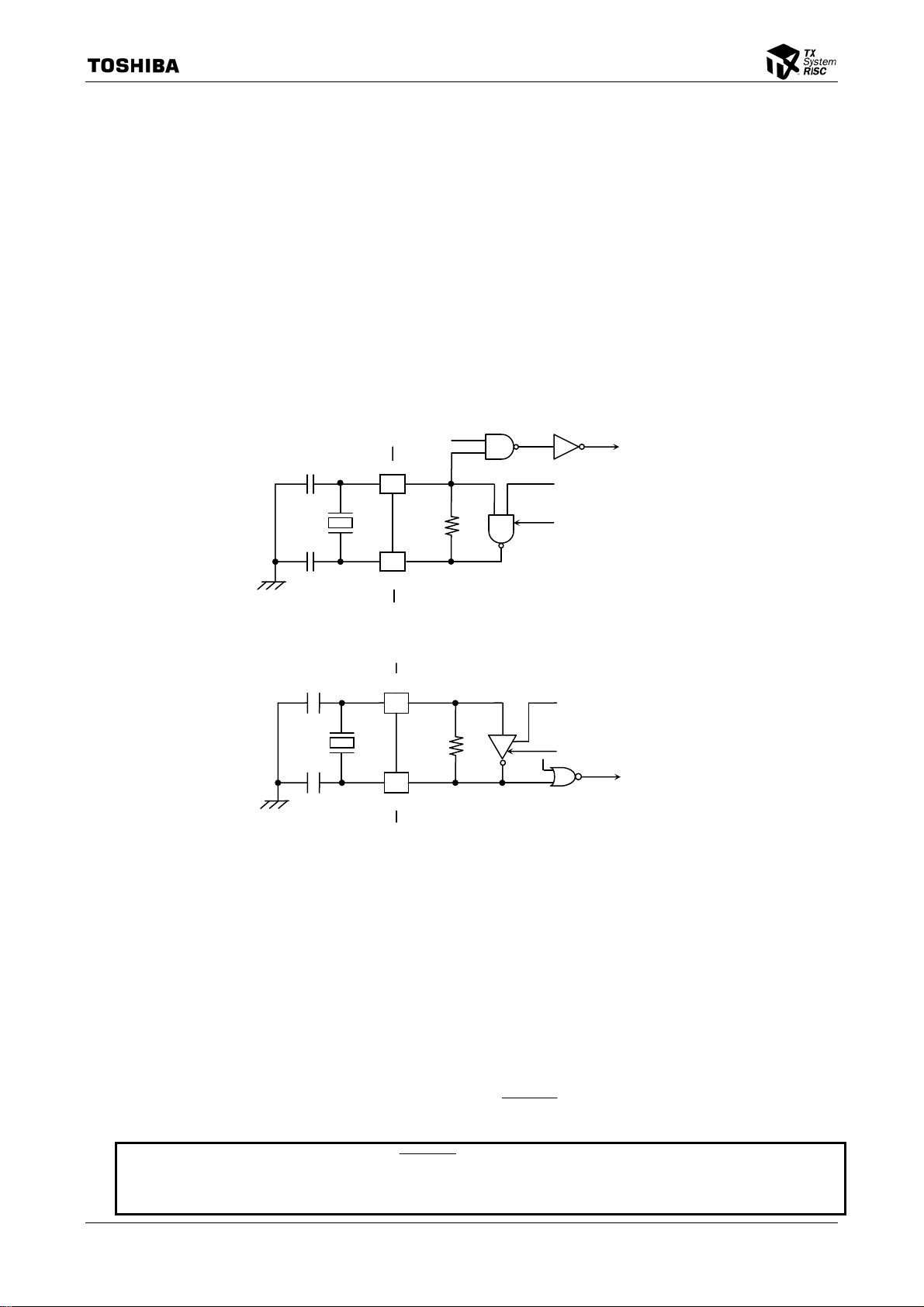
1) Reducing the driving capability of the high-speed oscillator
C1
X1 pin
Resonator
C2
Oscillation enable
SYSCR2<DRVOSCH>
f
OSC
X2 pin
2) Reducing the driving capability of the low-speed oscillator
C1
Resonator
C2
XT1 pin
XT2 pin
Oscillation enable
SYSCR2<DRVOSCL>
f
S
3.3.4 Prescaler clock control unit
The internal I/O blocks (TMRA01 to TMRAAB, TMRB0 to TMRBD, SIO0 to SIO5, SBI, and ADC)
each incorporate a prescaler for dividing the clock frequency. The clock φT0 fed into these prescalers is
derived from the clock fperiph. fperiph is either fgear or fc (as specified by the value of
SYSCR1<FPSEL>) divided by either 4 or 2, or not divided (as specified by the value of
SYSCR0<PRCK1:PRCK0>. By default, fperiph is set to fgear and φT0 to fperiph/4.
3.3.5 Clock multiplication circuit (PLL)
This circuit multiplies the high-speed oscillator outpu t clock, fosc, by 4 and outputs the result as the
clock fpll. This enables the oscillator to yield a fast internal clock with a low oscillator frequency . The
PLL is halted by a reset. To use the PLL, hold the
Note: If a reset is terminated while the
clock chosen will be the original oscillating clock (i.e., it will not be multiplied by 4).
PLLOFF pin High when terminating a reset.
PLLOFF pin is held Low, the PLL will not work and the internal
TMP1942CY/CZ-27

Since the PLL is configured as an analog circuit, it requires a certain settling time (a lock-up time) after
it has been activated, as does the oscillator.
The same timer is used for both warm-up and lock-up. The lock-up time must be set using
SYSCR3<LUPTM> so that it satisfies the following relationship:
Lock-up time ≥ warm-up time
By default, the lock-up time is 2
The lock-up timer is initiated as the high-speed oscillator starts warm-up, and the lock-up flag
SYSCR3<LUPTM> remains 1 until the PLL is locked in phase and cleared to 0 upon the completion of
lock-up.
If, for example, the PLL gets out of lock in a standby mode and control which depends on the software' s
execution speed, such as real-time processing, is to be performed, the software must check the lock-up
flag after operation has started (i.e., after warm-up has been completed) to ensure that the clock has
settled, before it starts processing.
On the other hand, various hardware settings and static processing, such as register and memory
initialization, can be executed before the lock-up flag has been cleared.
Note: The LUPFG bit is undefined when the
Precautions to be observed when switching clock gear:
Clock gear switchover is performed by writing a value to SYSCR1<GEAR1:GEAR0>. The clock gear
is not switched immediately after the write: a execution time equal to several clock cycles is required.
Therefore, one or more instructions following the clock gear switchover instruction may be executed
using the old clock gear value. If these instructions need to be executed using the new clock gear value,
insert a dummy instruction (which executes a write cycle only) after the clock gear switchover
instruction.
When using a clock gear, ma ke sure that the prescaler output φTn in eac h peripheral I/O bl ock satisfies
the following relationship:
φTn < fsys/2
16
/input frequency.
PLLOFF pin is Low (the PLL is not used).
TMP1942CY/CZ
For this purpose set the clock-related registers so that φTn is slower than fsys/2.
3.3.6 Standby control unit
If the Halt bit in the TX19 processor core's Config register is set in NORMAL mode, the device enters
one of the standby modes - IDLE, SLEEP or STOP - as determined by the contents of
SYSCR2<STBY1:STBY0>. If the Config register's Doze bit is set, the device enters IDLE mode
regardless of the setting of SYSCR2<STBY1:STBY0>.
Features of the IDLE, SLEEP and STOP modes are described below.
1) IDLE: In this mode, only the CPU stops.
In the register corresponding to each module there is an IDLE mode run/stop setup bit for
internal I/O. This allows each m odule t o be s et i ndepe ndent ly to run or st op whil e the devi ce is
in IDLE mode. Table 3.3.3 lists the IDLE setup registers available for each internal I/O
m
odule.
TMP1942CY/CZ-28

TMP1942CY/CZ
Table 3.3.3 IDLE Mode Internal I/O Setup Registers
Internal I/O IDLE Mode Setup Register
TMRA01 TA01RUN<I2TA01>
TMRA23 TA23RUN<I2TA23>
TMRA45 TA45RUN<I2TA45>
TMRA67 TA67RUN<I2TA67>
TMRA89 TA89RUN<I2TA89>
TMRAAB TAABRUN<I2TAAB>
TMRB0 TB0RUN<I2TB0>
TMRB1 TB1RUN<I2TB1>
TMRB2 TB2RUN<I2TB2>
TMRB3 TB3RUN<I2TB3>
TMRB4 TB4RUN<I2TB4>
TMRB5 TB5RUN<I2TB5>
TMRB6 TB6RUN<I2TB6>
TMRB7 TB7RUN<I2TB7>
TMRB8 TB8RUN<I2TB8>
TMRB9 TB9RUN<I2TB9>
TMRBA TBARUN<I2TBA>
TMRBB TBBRUN<I2TBB>
TMRBC TBCRUN<I2TBC>
TMRBD TBDRUN<I2TBD>
SIO0 SC0MOD1<I2S0>
SIO1 SC1MOD1<I2S1>
SIO3 SC3MOD1<I2S3>
SIO4 SC3MOD1<I2S4>
SIO5 SC4MOD1<I2S5>
SBI SBI0BR1<I2SBI0>
A/D converter ADMOD1<I2AD>
WDT WDMOD<I2WDT>
Note 1: In Halt mode (entered when the Halt bit in the Config Register is set), the TX19 processor
core stops processor operation while maintaining the pipeline status. Since it does not
respond to requests for control of the bus from interna l DMA, it retains control of the bus.
Note 2: In Doze mode (entered when the Doze bit in the Config Register is set), the TX19 processor
core stops processor operation while maintaining the pipeline status. In this mode, it can
respond to requests for control of the bus from devices extern al to the processor core.
2) SLEEP: Only the internal low-speed oscillator, timer for real-time clock, 2-phase pulse input counter,
and KWUP (dynamic pull-up) operate.
3) STOP: The CPU runs with the low-spee d clock. The INTC, timer for real-time clock, WDT, 2-phase
pulse input counter, KWUP (dynamic pull-up), PIO, and EBIF can operate. Operation of other
peripheral functions is not guaranteed.
4) SLOW: All of the internal circuits stop.
TMP1942CY/CZ-29
TMP1942CY/CZ
(1) Operating status in each mode
Table 3.3.4 Operating Status in Each Mode
Operation Mode Operating Status
NORMAL The TX19 processor core and peripheral I/O both operate at the maximum frequency.
IDLE (Halt) The TX19 processor core, INTC, timer for real-time clock, WDT, 2-phase pulse input counter,
KWUP (dynamic pull-up), PIO, and EBIF operate with the low-speed clock.
IDLE (Doze) Processor operation stops and peripheral I/O operates as specified.
SLEEP Processor operation stops. Only the internal low-speed oscillator, timer for real-time clock,
STOP Processor and peripheral I/O operation stops completely.
2-phase pulse input counter, and KWUP (dynamic pull-up) operate (fs).
(2) CG operation in each mode
Table 3.3.5 CG Status in Each Operating Mode
Clock Source Mode Oscillator PLL Clock Supply to Peripheral I/O Clock Supply to the CPU
Resonator
External input
NORMAL ○ ○ ○ ○
SLOW ○ × Partially supplied (Note) ○
IDLE (Halt) ○ ○ Selectable ×
IDLE (Doze) ○ ○ Selectable ×
SLEEP fs only × Timer for real-time clock, 2-phase pulse
input counter, and dynamic pull-up
STOP
NORMAL × ○ ○ ○
SLOW × × Partially supplied(Note) ○
IDLE (Halt) × ○ Selectable ×
IDLE (Doze) × ○ Selectable ×
SLEEP × × Timer for real-time clock, 2-phase pulse
STOP
× × × ×
input counter, and dynamic pull-up
× × × ×
×
×
Note: This includes the INTC, EBIF (external bus interface), I/O ports, WDT, and timer for real-time clock.
(3) Operation of circuit blocks in each mode (○: Operating, ×: Idle)
Table 3.3.6 Circuit Block Operating Status in Each Mode
Circuit Block Clock Source IDLE (Doze) IDLE (Halt) SLEEP STOP
TX19 processor core
DMAC
INTC
EBIF
External bus right
PIO
DA
ADC
SIO
I2C
Timer counter
WDT
2-phase pulse input counter
Dynamic pull-up
Timer for real-time clock
CG
×
○
○
○
○
fsys
Fsys/fs
Fs ○ ○ ○
fs ○ ○ ○
⎯ ○ ○ ○ ×
○
○
Can be selected to run or stop for
each module independently.
×
×
○
○
○
×
○
×
×
×
×
×
×
× (*1)
×
×
×
×
×
(fs only)
×
×
×
×
×
×
× (*1)
×
×
×
×
×
×
×
×
*1: DAC output is controlled with the OP bit for each channel.
TMP1942CY/CZ-30

TMP1942CY/CZ
(4) Terminating a standby mode
The device can be freed from a standby mode by an interrupt request or a reset. The combination
of the interrupt mask register <CMask15:13> setting and the current standby mode determines
which interrupt source will be used to terminate the standby mode. The interrupt mask register is part
of the Status register in the TX19 processor core's system control coprocessor (CP0). Details are
given in Table 3.3.7.
• T
ermination by an interrupt request
The operation performed when t he device is released from a standby mode by an interr upt request
varies according to the interrupt enable status. If the interrupt level which was set before the device
entered the standby mode is greater than or equal to the value in the interrupt mask register, the
processor services the requested interrupt after exiting the standby mode and then begins executing
instructions starting with the one following the instruction to enter the standby mode (i.e., the
instruction which specified the appropriate Config register bit). If the interrupt request level is less
than the value in the interrupt mask register, the processor immediately begins executing instruct ions
starting with the one following the instruction to enter the standby mode (i.e., the instruction which
specified the appropriate Config register bit) without servicing the requested interrupt. (The interrupt
request flag remains 1.)
Non-maskable interrupts are always serviced after standby mode has terminated, irrespective of
the value of the mask register.
• Termination by a reset
The device can be released from any standby m ode by a rese t. However, after release from STOP
mode, a certain reset time is required for oscillator operation to settle. The reset selects a warm-up
time of 2
14
/oscillation frequency.
After release by a reset, the internal RAM data can be retained in the state in which it was placed
immediately before the standby mode was entered; however, all other settings will be initialized.
(After released by an interrupt, other settings are also retained in the state in which they were placed
immediately before the standby mode was entered.)
Table 3.3.7 Standby Termination Sources and Standby Termination Operation
Interrupt Acceptance State
Standby mode
NMI *1
INTWDT × × × ×
INT0~4, INTB~E
KWUP0~D
INTRTC × ○ ○ ×
INT5~A × × ○ × ×
Interrupt
INTTA0~B × × ○ × ×
INTTB0~D (*2) × ○ ○ (*2) ×
INTRX0~5, TX0~5
INTS2
Standby mode termination source
INTAD/ADHP/ADM
RESET
Interrupt Enabled
(Interrupt level) > (Interrupt mask)
IDLE
(programmable)
SLEEP STOP
×
×
×
*1
*1
×
×
×
(Interrupt level) ≤ (Interrupt mask)
(programmable)
Interrupt Enabled
IDLE
○
○
○
○
○
SLEEP STOP
○
○
×
×
×
○*1
○*1
×
×
×
: After exiting the standby mode, the processor starts servicing the interrupt. (RESET initializes the LSI.)
○: After exiting the standby mode, the processor begins executing instructions starting with the one
following the instruction to enter the standby mode, without servicing the interrupt.
TMP1942CY/CZ-31
TMP1942CY/CZ
×: Cannot be used to exit from a standby mode.
*1: The device is actually released from the standby mode after the warm-up time has passed.
*2: Only INTTB2 and INTTB3 can be used when 2-phase pulse input counter mode is selected.
Note 1: When using a level-sensitive interrupt to terminate a standby mode, be sure to hold the level until the
processor starts servicing the interrupt. If the level is changed before that time, the interrupt cannot
be serviced properly.
Note 2: If the interrupts are disabled in the CPU, use the interrupt controller (INTC) to disable only the
interrupts other than those used for terminating standby, before placing the device in any of the
standby modes.
(5) STOP mode
In STOP mode all internal circuits, including the internal oscillator, stop operating. The pin state
in STOP mode varies acc ordin g to the setting of SYSC R2<DR VE>, as shown in Table 3.3.10. Once
released from STOP mode, the device waits for a while (until the warm-up tim e ends) before starting
to output the system clock; the warm-up time is counted by the warm-up counter. This delay is to
ensure that the internal oscillator settles properly. After exiting STOP mode the device starts
operating according to the settings of SYSCRO<RXEN, RXTEN, RSYSCK>, which select the
operating mode (NORMAL mode or SLOW mode) to be entered on exit from STOP mode.
These settings must be made before the instruction to enter standby mode is executed. The
warm-up time is determined by the setting of SYSCR2<WUPT1:WUPT0>.
(6) Timing of terminating STOP/SLEEP mode
1) Operation mode transition from Normal through Stop to Normal
fsys
(high-speed clock)
System clock stopped
Mode
CG
(high-speed clock)
Warm-up (W-up)
Normal
When fosc = 8 MHz
W-up time selection
SYSCR2<WUPT1:0>
00(22/fosc)
01(28/fosc)
10(214/fosc) 2.048 ms
11(216/fosc) 8.192 ms
Warm-up started Warm-up finished
W-up time
(fc)
Not allowed
Not allowed
Stop Normal
High-speed
clock oscillation started
Note:<WUPT1:WUPT0> must not be set to 00 or 01
resuming time requirements for the internal
system.
TMP1942CY/CZ-32

2) Operation mode transition from Normal through Sleep to Normal
fsys
(high-speed clock)
System clock stopped
TMP1942CY/CZ
Mode
CG
(high-speed clock)
CG
(low-speed clock)
Warm-up (W-up)
Normal
Low-speed clock (fs) continues oscillation.
When fosc = 8 MHz
W-up time selection
SYSCR2<WUPT1:0>
01(22/fosc)
01(28/fosc)
10(214/fosc)
11(216/fosc)
W-up time
(fc)
Not allowed
Not allowed
2.048 ms
8.192 ms
Warm-up started Warm-up finished
Sleep Normal
Low-speed clock (fs) continues oscillation.
High-speed
clock oscillation started
Note:<WUPT1:WUPT0> must not be set to 00 or 01
because those settings would not satisfy the
resuming time requirements for the internal system.
3) Operation mode transition from Slow through Stop to Slow
fsys
(low-speed clock)
Mode
Slow
System clock stopped
Stop Slow
CG
(low-speed clock)
Warm-up (W-up)
When fs = 32.768 MHz
W-up time selection
SYSCR2<WUPT1:0>
01(22/fosc) Not all owed
01(28/fosc) 7.8 ms
10(214/fosc) 500 ms
11(216/fosc) 2000 ms
W-up time
Low-speed clock
oscillation started
Warm-up started Warm-up finished
(fc)
4) Operation mode transition from Slow through Sleep to Slow
fsys
(low-speed clock)
Mode
CG
(low-speed clock)
Warm-up (W-up)
Slow
When fs = 32.768 MHz
W-up time selection
SYSCR2<WUPT1:0>
01(22/fs) 122 μs
01(28/fs) 7.8 ms
10(214/fs) 500 ms
11(216/fs) 2000 ms
W-up time
System clock stopped
Sleep Slow
Low-speed clock
continues oscillation.
Warm-up started Warm-up finished
(fc)
Note: fs continues oscillation but the warm-up time need
be set. Set <WUPT1:WUPT0> to 00.
TMP1942CY/CZ-33

Table 3.3.8 Pin States in STOP Mode (1/2)
TMP1942CY/CZ
Pins Input/Output <DRVE> = 0 <DRVE> = 1
AD0~AD7 Input/Output - AD8~AD15 Input/Output - A0~A7/A16~A23
, Output - Output
RD
WR
, Input PU* Input
HWR
BUSRQ
WAIT
, , Output PU* Output
BUSAK
W/R
Output - Output
P37 Output mode
Input mode PU* Input P40~43
Output mode PU* Output
Input mode - Input P44 (SCOUT)
Output mode - Output
P50~57 Input pin - P60~67 Input pin - -
Input
Input Input
mode(KEY0~KEY7)
P90~P91 Input mode - Input
Output mode - Output
Input mode(INT3,INT4) Input Input
Input mode - Input P92~97
Output mode - Output
PA0~PA1 Input mode - Input
Output mode - Output
Input mode(INT3,INT4) Input Input
PA2~PA7 Input mode - Input
Output mode - Output
PA7 Input mode - Input
Output mode - Output
Input mode(KEYA) Input Input
PB1~PB4 Input mode - Input
Output mode - Output
Input mode(INTB~INTE) Input Input
PB0,PB5~PB6 Input mode - Input
Output mode - Output
PB7 Input mode - Input
Output mode - Output
Input mode(KEYB) Input Input
PC0~PC5,PC7 Input mode - Input
Output mode - Output
PC6 Input mode - Input
Output mode - Output
Input mode(KEYB) Input Input
PD0~PD5 Input mode - Input
Output mode - Output
PD6 (XT1)~
PD7 (XT2)
Input mode - Input
Output mode - Output
XT1, XT2 - -
TMP1942CY/CZ-34

TMP1942CY/CZ
Pins Input/Output <DRVE> = 0 <DRVE> = 1
PE0~PE5 Input mode - Input
Output mode - Output
PE6~PE7 Input mode - Input
Output mode - Output
Input mode(INT1,INT2) Input Input
PF0,PF2~PF5 Input mode - Input
Output mode - Output
PF1 Input mode - Input
Output mode - Output
Input mode(KEYD) Input Input
PF6 Input mode - Input
Output mode - Output
Input mode(INT0) Input Input
Input pin Input Input
NMI
ALE Output pin Output Low Output Low
Input pin Input Input
RESET
BW0, BW1 Input pin Input Input
X1 Input pin - X2 Output pin Output High Output High
-: Pins configured for input mode and input-only pins are disabled. Pins configured for output mode and
output-only pins assume the high-Impedance state.
Input: The input gate is active; the input voltage must be held at either the high or low level to keep the input
pin from floating.
Output: Pin direction is output.
PU*: Programmable pull-up. Because the input gate is always disabled, no overlap current flows while in
high-impedance state.
TMP1942CY/CZ-35

3.4 Interrupts
Interrupts are controll ed by th e Status <CMask15:13> and S tatus<IEc> settings in the CP0 status register, as
well as by the internal interrupt controller and the CG. For related information, refer to Section 5, “Exception
Handling” in “TX19 Family Architecture”.
Interrupts in the TMP1942 have the following features:
• Interrupts from the CPU itself (software interrupt instructions): 4 sources
TMP1942CY/CZ
• External interrupt pins (
• Interrupts from internal I/O: 46 sources
• Vector generation for each interrupt source
• 7 interrupt priority levels for each source
• Can be used to activate the DMAC
NMI , INT0-INTE, KWUP0-KWUPD): 30 sources
TMP1942CY/CZ-36

TMP1942CY/CZ
CG
INTnEN standby
termination
8
control
Detection circuit
INTC
Active
High level
8
8
High or Low
level/edge
setting
High level
High level
5
1
1
INT0∼4
Core
High level
7
Other
interrupts
Active High level
KWUP
High or Low
level/edge setting
KEY0
∼D
RTC
Disable/enable each
key input
Active High level
Extended interrupts
High or Low
level/edge setting
INTB
∼E
Disable/enable input
for each interrupt
source
Note 1: Standby termination is performed via the CG detection circuit. Since its output is a High-level active signal, the INTC must be
set to accept a High-level active signal.
Note 2: The CG is bypassed for an y proc essing other tha n standby termination. In that case, the active con ditions for INT 0 to I NT4
must be set in the INTC.
Note 3: INTRTC requires CG settings for both standby termination and other processing. The INTC must be set to accept a
High-level active signal.
Note 4: KWUP and INTB to INTD require settings in each circuit block for both standby termination and other processing. The INTC
must be set to accept a High-level active signal.
Figure 3.44.1 Interrupt Connection Diagram
TMP1942CY/CZ-37

(1) External interrupts INT0 to INT4, INTB to INTE, KWUP0 to KWUPD, and INTRTC
1) INT0 to INT4
When used to terminate a standby mode, these interrupts must have their active state set (using
IMCGxx<EMCGxx>) and must be enabled for input (using IMCGxx<INTxEN>) in the CG block.
Then the active state of each of the interrupt source must be set to High (by setting IMC xx<EIMxx> to
01) in the INTC block. When these interrupts are not used to terminate a standby m ode, set their active
state in the INTC block.
2) INTB to INTE
When used to terminate a standby mode, these interrupts must have their active state set to High (by
setting IMCGB2<21:20> to 10) and must be enabled for input (by setting IMCGB2<16> to 1) in the
CG block. Then the active state of each of the interrupt source must be set to High (by setting
IMCxx<EIMxx> to 01) in the INTC block. Use INTnST for each interrupt source to set the active state
and enable or disable the interrupt. When these interrupts are not used to terminate a standby mode,
make necessary settings in the INTC block and INTnST without having to make settings in the CG.
3) KW
4) INTRTC
UP0 to KWUPD
When used to terminate a standby mode, these interrupts must have their active state set to High (by
setting IMCGB1<21:20> to 10) and must be enabled for input (by setting IMCGB1<16> to 1) in the
CG block. Then the active state of each of the interrupt source must be set to High (by setting
IMCxx<EIMxx> to 01) in the INTC block. Use KWUPSTn for each interrupt source to set the active
state and enable or disable the interrupt. When these interrupts are not used to terminate a standby
mode, make necessary settings in the INTC block and KWUPSTn without having to make settings in
the CG.
Regardless of whether INTRTC is used to terminate a standby mode, this interrupt must have its active
state set to a rising edge (by setting IMCGB3<29:28> to 11) and must be enabled for input (by setting
IMCGB3<24> to 1) in the CG block. Then the active state of each of the interrupt s ource must be set to
High (by setting IMCxx<EIMxx> to 01) in the INTC block.
TMP1942CY/CZ
TMP1942CY/CZ-38

TMP1942CY/CZ
(2) External interrupts INT5 to INTA and internal interrupt signals (other than INTRTC)
All these interrupts must be set in the INTC block.
The INTC resolves priority conflicts between interrupt sources and notifies the TX19 processor core of
the interrupt with the highest priority.
Interrupt Register to be Set Usable Interrupt Detection Level
INT0∼INT4, INTRTC* IMCGx reg.In CG
IMCx reg.In INTC
INTB∼INTE IMCGx reg.In CG
IMCx reg.In INTC
INTnST
KWUP0∼D IMCGx reg.In CG
IMCx reg.In INTC
KWUPSTn
INT5∼INTA IMCx reg.In INTC Low level, High level, falling edge and rising edge are all acceptable in the
Internal I/O INTDMAn IMCx reg.In INTC Falling edge
Others IMCx reg.In INTC Rising edge
When used to terminate a standby mode, the interrupt source active state
must be set to High in the INTC block. The active state of these interrupts
must be selected in the CG. However, when these interrupts are not used to
terminate a standby mode, their active state must be selected in the INTC
block. In both cases, Low level, High level, falling edge and rising edge are all
acceptable.
The interrupt source active state must always be set to High in the INTC
block. When these interrupts are used to terminate a standby mode, the
interrupt source active state must also be set to High in the CG. The active
state of these interrupts must be selected in INTnST. However, when these
interrupts are not used to terminate a standby mode, settings in the CG are
not necessary. In both cases, Low level, High level, falling edge and rising
edge are all acceptable.
The interrupt source active state must always be set to High in the INTC
block. When these interrupts are used to terminate a standby mode, the
interrupt source active state must also be set to High in the CG. The active
state of these interrupts must be selected in KWUPSTn. However, when
these interrupts are not used to terminate a standby mode, settings in the CG
are not necessary. In both cases, Low level, High level, falling edge and rising
edge are all acceptable.
INTC.
Note 1: Interrupt level 0 indicates that the corresponding interrupt is disabled.
Note 2: Only a rising edge can be used for INTRTC.
• Example interrupt settings
When INT0 is used to request the termination of STOP/SLEEP mode (falling edge)
a. Enabling the interrupt
IMCGA0<EMCG01:00> = “10” : Select falling edge for INT0
EICRCG<ICRCG2:0> = “000” : Clear interrupt request for INT0 CG block
IMCGA0<INT0EN> = “1” : Enable request input for INT0
IMC0L<EIM11:10> = “01” : Select High level for INT0
INTCLR<EICLR5:0> = “000001” : Clear interrupt request for INT0 INTC block
IMC0L<IL12:10> = “101” : Set in
terrupt level to 5
Status<IEc> = “1”, <CMask> = “xxx” TX19 processor core
b. Disabling the interrupt
Status<IEc> = “0” TX19 processor core
IMC0L<IL12:10> = “000” : Disable interrupt for INT0
INTCLR<EICLR5:0> = “000001” : Clear interrupt request for INT0
IMCGA0<INT0EN> = “0” : Disable request input for INT0
EICRCG<ICRCG2:0> = “000” : Clear interrupt request for INT0
INTC block
CG block
TMP1942CY/CZ-39

3.4.1 Interrupt sources
(1) Reset and non-maskable interrupts: RESET , NMI and INTWDT (watchdog timer interrupt)
Vector address: 0xBFC0_0000 (virtual address)
(2) Maskable interrupts: Software and hardware interrupts
Vector addresses: 0xBFC0_0210 (virtual address) to 0xBFC0_0260 (virtual address)
Note 1: When vector addresses are located in the on-chip ROM, set the BEV bit in the
Note 2: Maskable software interrupts are generated by setting <Sw3:Sw0> in CP0
TMP1942CY/CZ
Interrupt Source Vector Address (virtual address)
Reset
Non-maskable
Software Swi0 0xBFC0_0210
Swi1 0xBFC0_0220
Swi2 0xBFC0_0230
Swi3 0xBFC0_0240
Maskable
Hardware 0xBFC0_0260
system control coprocessor (CP0) Status register to 1.
Cause register. Do not confuse these software interrupts with Software Set,
which is one of the hardware interrupt sources. The Soft ware Set interrupt is
generated by setting <IL02:IL00> in the interrupt controller (INTC) IMC0 register
to any value other than 0.
0xBFC0_0000
TMP1942CY/CZ-40

TMP1942CY/CZ
Table 3.44.1 Hardware Interrupt Sources
Interrupt Number IVR[9 : 0] Interrupt Source Interrupt control register Address
0
1
2
3
4
5
6
7
8
9
10
11
12
13
14
15
16
17
18
19
20
21
22
23
24
25
26
27
28
29
30
31
32
33
34
35
36
37
38
39
40
41
42
43
44
45
46
47
48
49
50
51
52
53
54
55
56
57
58
59
60
61
62
63
000
010
020
030
040
050
060
070
080
090
0A0
0B0
0C0
0D0
0E0
0F0
100
110
120
130
140
150
160
170
180
190
1A0
1B0
1C0
1D0
1E0
1F0
200
210
220
230
240
250
260
270
280
290
2A0
2B0
2C0
2D0
2E0
2F0
300
310
320
330
340
350
360
370
380
390
3A0
3B0
3C0
3D0
3E0
3F0
Software Set
INT0 pin (standby termination)
INT1 pin (standby termination)
INT2 pin (standby termination)
INT3 pin (standby termination)
INT4 pin (standby termination)
KWUP (standby termination)
INTB/C/D/E pin (standby termination)
Reserved
Reserved
INT5 pin
INT6 pin
INT7 pin
INT8 pin
INT9 pin
INT
A pin
INTRX0: Serial reception (channel 0)
INTTX0: Serial transmission (channel 0)
INTRX1: Serial reception (channel 1)
INTTX1: Serial transmission (channel 1)
INTS2: Serial channel 2 interrupt
INTRX3: Serial reception (channel 3)
INTTX3: Serial transmission (channel 3)
INTADHP: Highest-priority A/D conversion completed
INTADM: A/D conversion monitor interrupt
INTTA0: 8-bit timer 0
INTTA1: 8-bit timer 1
INTTA2: 8-bit timer 2
INTTA3: 8-bit timer 3
INTTB0: 16-bit timer 0
INTTB1: 16-bit timer 1
INTRX4: Serial reception (channel 4)
INTTX4: Serial transmission (channel 4)
INTRX5: Serial reception (channel 5)
INTTX5: Serial transmission (channel 5)
Reserved
Reserved
INTTA4: 8-bit timer 4
INTTA5: 8-bit timer 5
INTTA6: 8-bit timer 6
INTTA7: 8-bit timer 7
INTTA8: 8-bit timer 8
INTTA9: 8-bit timer 9
INTTAA: 8-bit timer A
INTTAB: 8-bit timer B
INTTBA: 16-bit timer A
INTTBB: 16-bit timer B
INTTBC: 16-bit timer C
INTTBD: 16-bit timer D
INTTB2: 16-bit timer 2
INTTB3: 16-bit timer 3
INTTB4: 16-bit timer 4
INTTB5: 16-bit timer 5
INTTB6: 16-bit timer 6
INTTB7: 16-bit timer 7
INTTB8: 16-bit timer 8
INTTB9: 16-bit timer 9
Reserved
INTRTC: Interrupt from timer for real-time clock
INTAD: A/D conversion completed
INTDMA0: DMA transfer completed (channel 0)
INTDMA1: DMA transfer completed (channel 1)
INTDMA2: DMA transfer completed (channel 2)
INTDMA3: DMA transfer completed (channel 3)
IMC0L
IMC0H
IMC1L
IMC1H
IMC2L
IMC2H
IMC3L
IMC3H
IMC4L
IMC4H
IMC5L
IMC5H
IMC6L
IMC6H
IMC7L
IMC7H
IMC8L
IMC8H
IMC9L
IMC9H
IMCAL
IMCAH
IMCBL
IMCBH
IMCCL
IMCCH
IMCDL
IMCDH
IMCEL
IMCEH
IMCFL
IMCFH
0xF
FFF_E000
0xFFFF_E002
0xFFFF_E004
0xFFFF_E006
0xFFFF_E008
0xFFFF_E00A
0xFFFF_E00C
0xFFFF_E00E
0xFFFF_E010
0xFFFF_E012
0xFFFF_E014
0xFFFF_E016
0xFFFF_E018
0xFFFF_E01A
0xFFFF_E01C
0xFFFF_E01E
0xFFFF_E020
0xFFFF_E022
0xFFFF_E024
0xFFFF_E026
0xFFFF_E028
0xFFFF_E02A
0xFFFF_E02C
0xFFFF_E02E
0xFFFF_E030
0xFFFF_E032
0xFFFF_E034
0xFFFF_E036
0xFFFF_E038
0xFFFF_E03A
0xFFFF_E03C
0xFFFF_E03E
TMP1942CY/CZ-41

3.4.2 Interrupt detection
When using interrupts to terminate a standby mode, the following settings are necessary according to
the interrupt type: Interrupts INT0 to INT4 have their active state set using the EMCGxx field in the CG's
internal IMCGxx register, then the EIMxx field in the INTC's internal IMCx register is set to High.
Extended interrupts INTB to INTE have their active state set to High using the EMCG field in the CG's
internal IMCGB2 register, then the EIMxx field in the INTC's internal IMCx register is set to High. In
addition, INTnST is used to set the active state for each interrupt source and enable/disable the interrupt
source. KWUP0 to KWUPD have their active state set to High using the EMCG field in the CG's internal
IMCGB1 register, then the EIMxx field in the INTC's internal IMCx register is set to High. In addition,
KWUPSTn is used to set the active state for each interrupt source and enable/disable the interrupt source.
The RTC interrupt has its active state set to a rising edge using the EMCGxx field in the CG's internal
IMCGxx register, then the EIMxx field in the INTC's internal IMCx register is set to High. Other
interrupts have their active state set using only the EIMxx field in the INTC's internal IMCx register. The
active state can be one of the following four: rising edge, falling edge, High level or Low level. When the
TMP1942 detection circuit recognizes the active state of an interrupt request set in this way, it notifies the
processor core or the INTC of the interrupt request. When the above interrupts are not used to terminate a
standby mode, settings in the CG are not required: INT0 to INT4 require only settings in the INTC, INTB
to INTE require the same settings in the INTC as for standby termination as well as setting in INTnST,
and KWUP0 to KWUPD require the same settings in the INTC as for standby termination as well as
setting in KWUPSTn.
Cancellation of interrupt signals is carried out by the interrupt handler after it has recognized the
requested interrupt.
INTB to INTE are canceled by reading INTFLG.
Interrupt signals from INT0 to INT4 and INTRTC are cancelled by writing the appropriate value to the
ICRCG field in the CG's internal EICRCG register and then writing the corresponding value to the
EICLR field in the INTC's internal INTCLR register. KWUP0 to KWUPD are canceled by setting
KW
UPCLR. Other interrupt signals are canceled by writing the appropriate value to the EICLR field in
the INTC's internal INTCLR register. These cancellation procedures apply regardless of whether the
active state is an edge or level.
TMP1942CY/CZ
TMP1942CY/CZ-42

∼
TMP1942CY/CZ
Start
INT0
∼A/
INTRTC*
Interrupt?
Set INTC
INTB
∼E
KWUP0
∼D INT0
Set KWUPSTn or
INTnST
Set INTC (High level)
NO
INTRTC
Set CG
Standby termination
4
YES
Interrupt?
INTB
KWUP0
∼E
∼D
Set INTC (High level)
Set KWUPSTn or INTnST
Set CG (High level)
Set INTC (High level)
End
* The INTRTC interrupt must have its active state set to a rising edge in the CG even when it is not
used for standby termination.
Figure 3.44.2 Flow for Setting External Interrupts
Note: Each stage must be completed in the following sequence: set the active level, clear the
interrupt request, and then enable the interrupt.
(Example of setting INT0 for standby termination)
IMCGA0<EMCG01:00> = “10” : Select falling edge for INT0
EICRCG<ICRCG2:0> = “000” : Clear interrupt request for INT0C G block
IMCGA0<INT0EN> = “1” : Enable request input for INT0
IMC0L<EIM11:10> = “01” : Select High level for INT0
INTCLR<EICLR5:0> = “000001” : Clear interrupt request for INT0 INTC block
IMC0L<IL12:10> = “101” : Set in
terrupt level to 5
Status<IEc> = “1”, <CMask> = “xxx” TX19 processor core
TMP1942CY/CZ-43

3.4.3 Resolving interrupt priority
(1) Seven interrupt priority levels
The TMP1942 has seven interrupt priority levels; thus for each interrupt source the priority can be
set to one of seven levels.
The interrupt mode control register (IMCx) is used for setting interrupt levels. This register
includes a 3-bit level-setting field (ILx). The greater the value (interrupt level) set in
IMC<ILx2:ILx0>, the higher the interrupt priority. If the value set for an interrupt source in this field
is 000 (i.e., the interrupt level is set to 0), no interrupt is generated for that interrupt source.
(2) Notification of the interrupt level
When an interrupt occurs, the INTC notifies the TX19 processor core of the priority level of the
interrupt. The TX19 processor core recognizes the interrupt level by reading the IL field in the Cause
register. If multiple interrupts (with different priority levels) occur simultaneously, the TX19
processor core is notified of the interrupt with the highest priority.
(3) Interrupt vector (notification of interrupt source)
When an interrupt occurs, t he INTC also set s the vector fo r the source of t he generated i nterrupt in
the vector register (IVR). The TX19 processor core reads the vector register to determine the
interrupt source. If multiple interrupts (with the same priority level) occur sim ultaneously , the TX19
processor core is notified of the vector for the interrupt source with the smallest request number.
Whe
n there are no interrupt sources for which an interrupt has occurred, the IVR[9:4] field is 0.
When it is time for the TX19 processor core to read the vector register value, the INTC notifies the
processor core. The processor core sets the Status<CMask> bit with the interrupt level wh ich it
reads.
TMP1942CY/CZ
TMP1942CY/CZ-44
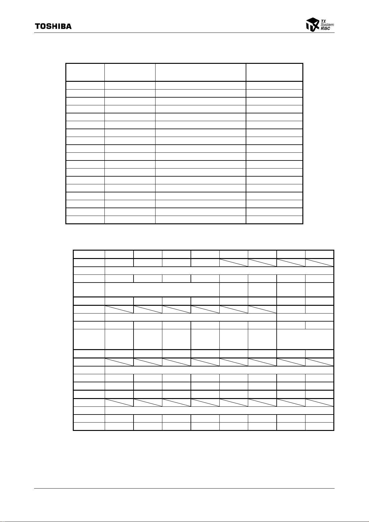
3.4.4 INTC registers
Table 3.44.2 INTC Register Map
TMP1942CY/CZ
Address Register Symbol Register
0xFFFF_E060 INTCLR Interrupt request clear control ALL (63 − 0)
0xFFFF_E040 IVR Interrupt vector register ALL (63 − 0)
0xFFFF_E03C IMCF Interrupt mode control register F 63 − 60
0xFFFF_E038 IMCE Interrupt mode control register E 59 − 56
0xFFFF_E034 IMCD Interrupt mode control register D 55 − 52
0xFFFF_E030 IMCC Interrupt mode control register C 51 − 48
0xFFFF_E02C IMCB Interrupt mode control register B 47 − 44
0xFFFF_E028 IMCA Interrupt mode control register A 43 − 40
0xFFFF_E024 IMC9 Interrupt mode control register 9 39 − 36
0xFFFF_E020 IMC8 Interrupt mode control register 8 35 − 32
0xFFFF_E01C IMC7 Interrupt mode control register 7 31 − 28
0xFFFF_E018 IMC6 Interrupt mode control register 6 27 − 24
0xFFFF_E014 IMC5 Interrupt mode control register 5 23 − 20
0xFFFF_E010 IMC4 Interrupt mode control register 4 19 − 16
0xFFFF_E00C IMC3 Interrupt mode control register 3 15 − 12
0xFFFF_E008 IMC2 Interrupt mode control register 2 11 − 8
0xFFFF_E004 IMC1 Interrupt mode control register 1 7 − 4
0xFFFF_E000 IMC0 Interrupt mode control register 0 3 − 0
Corresponding
Interrupt Number
Interrupt vector register (IVR): Indicates the vector for the source of each interrupt generated.
IVR Bit Symbol IVR7 IVR6 IVR5 IVR4
(0xFFFF_E040) Read/Write R
After reset 0 0 0 0 0 0 0 0
Function Indicates the vectors for
7 6 5 4 3 2 1 0
generated interrupt sources.
15 14 13 12 11 10 9 8
Bit Symbol
Read/Write
After reset
Function
Bit Symbol
Read/Write
After reset
Function
Bit Symbol
Read/Write
After reset
Function
23 22 21 20 19 18 17 16
31 30 29 28 27 26 25 24
IVR9 IVR8
R/W R
0 0 0 0 0 0 0 0
Indicates the vectors for
generated interrupt
sources.
R/W
0 0 0 0 0 0 0 0
R/W
0 0 0 0 0 0 0 0
TMP1942CY/CZ-45
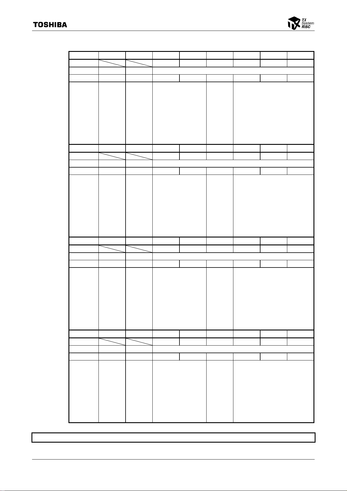
t
t
t
t
TMP1942CY/CZ
Interrupt mode control registers : Set the priority level and active state for each interrupt source and set
whether the interrupt is to be used to activate the DMAC.
7 6 5 4 3 2 1 0
IMC0 Bit Symbol EIM01 EIM00 DM0 IL02 IL01 IL00
(0xFFFF_E000) Read/Write R/W
After reset 0 0 0 0 0 0
Function
Sets the active state of
the interrupt request.
00: Low level
Other settings are not
allowed.
Sets
whether or
not to
activate the
DMAC.
0: Not set.
1: Set interrup
number 0 to
activate the
DMAC.
Sets the priority level for interrupt
number 0 (Software Set) when
DM0 = 0.
000: Disable interrupt.
001-111: 1 to 7
Selects a DMAC channel when
DM0 = 1.
000-011: 0 to 3
100-111: Invalid settings
15 14 13 12 11 10 9 8
Bit Symbol EIM11 EIM10 DM1 IL12 IL11 IL10
Read/Write R/W
After reset 0 0 0 0 0 0
Function
Sets the active state of
the interrupt request.
00: Low level
01: High level
10: Falling edge
11: Rising edge
Sets
whether or
not to
activate the
DMAC.
0: Not set.
1: Set interrup
number 1 to
activate the
DMAC.
Sets the priority level for interrupt
number 1 (INT0) when
DM1 = 0.
000: Disable interrupt.
001-111: 1 to 7
Selects a DMAC channel when
DM1 = 1.
000-011: 0 to 3
100-111: Invalid settings
23 22 21 20 19 18 17 16
Bit Symbol EIM21 EIM20 DM2 IL22 IL21 IL20
Read/Write R/W
After reset 0 0 0 0 0 0
Function
Sets the active state of
the interrupt request.
00: Low level
01: High level
10: Falling edge
11: Rising edge
Sets
whether or
not to
activate the
DMAC.
0: Not set.
1: Set interrup
number 2 to
activate the
DMAC.
Sets the priority level for interrupt
number 2 (INT1) when
DM2 = 0.
000: Disable interrupt.
001-111: 1 to 7
Selects a DMAC channel when
DM2 = 1.
000-011: 0 to 3
100-111: Invalid settings
31 30 29 28 27 26 25 24
Bit Symbol EIM31 EIM30 DM3 IL32 IL31 IL30
Read/Write R/W
After reset 0 0 0 0 0 0
Function Sets the active state of
the interrupt request.
00: Low level
01: High level
10: Falling edge
11: Rising edge
Sets
whether or
not to
activate the
DMAC.
0: Not set.
1: Set interrup
number 3 to
activate the
DMAC.
Sets the priority level for interrupt
number 3 (INT2) when
DM3 = 0.
000: Disable interrupt.
001-111: 1 to 7
Selects a DMAC channel when
DM3 = 1.
000-011: 0 to 3
100-111: Invalid settings
Note : Before enabling the above interrupt requests, be sure to set their active state.
TMP1942CY/CZ-46

o
o
o
o
TMP1942CY/CZ
7 6 5 4 3 2 1 0
IMC1 Bit Symbol EIM41 EIM40 DM4 IL42 IL41 IL40
(0xFFFF_E004) Read/Write R/W
After reset
Function
0 0 0 0 0 0
Sets the active state of
the interrupt request.
00: Low level
01: High level
10: Falling edge
11: Rising edge
Sets
whether or
not to
activate the
DMAC.
0: Not set.
1: Set
interrupt
number 4 t
activate the
DMAC.
Sets the priority level for interrupt
number 4 (INT3) when
DM4 = 0.
000: Disable interrupt.
001-111: 1 to 7
Selects a DMAC channel when
DM4 = 1.
000-011: 0 to 3
100-111: Invalid settings
15 14 13 12 11 10 9 8
Bit Symbol EIM51 EIM50 DM5 IL52 IL51 IL50
Read/Write R/W
After reset
Function
0 0 0 0 0 0
Sets the active state of
the interrupt request.
00: Low level
01: High level
10: Falling edge
11: Rising edge
Sets
whether or
not to
activate the
DMAC.
0: Not set.
1: Set
interrupt
number 5 t
activate the
DMAC.
Sets the priority level for interrupt
number 5 (INT4) when
DM5 = 0.
000: Disable interrupt.
001-111: 1 to 7
Selects a DMAC channel when
DM5 = 1.
000-011: 0 to 3
100-111: Invalid settings
23 22 21 20 19 18 17 16
Bit Symbol EIM61 EIM60 DM6 IL62 IL61 IL60
Read/Write R/W
After reset
Function
0 0 0 0 0 0
Sets the active state of
the interrupt request.
00: Low level
01: High level
10: Falling edge
11: Rising edge
Sets
whether or
not to
activate the
DMAC.
0: Not set.
1: Set
interrupt
number 6 t
activate the
DMAC.
Sets the priority level for interrupt
number 6 (KWUP) when
DM6 = 0.
000: Disable interrupt.
001-111: 1 to 7
Selects a DMAC channel when
DM6 = 1.
000-011: 0 to 3
100-111: Invalid settings
31 30 29 28 27 26 25 24
Bit Symbol EIM71 EIM70 DM7 IL72 IL71 IL70
Read/Write R/W
After reset
Function
0 0 0 0 0 0 0
Sets the active state of
the interrupt request.
00: Low level
01: High level
10: Falling edge
11: Rising edge
Sets
whether or
not to
activate the
DMAC.
0: Not set.
1: Set
interrupt
number 7 t
activate the
DMAC.
Sets the priority level for interrupt
number 7 (INTB/C/D/E) when
DM7 = 0.
000: Disable interrupt.
001-111: 1 to 7
Selects a DMAC channel when
DM7 = 1.
000-011: 0 to 3
100-111: Invalid settings
Note : Before enabling the above interrupt requests, be sure to set their active state.
TMP1942CY/CZ-47

TMP1942CY/CZ
7 6 5 4 3 2 1 0
IMC2 Bit Symbol EIM81 EIM80 DM8 IL82 IL81 IL80
(0xFFFF_E008) Read/Write R/W
After reset
Function
0 0 0 0 0 0
Must be set to 00. Must be
set to 0.
Must be set to 000.
15 14 13 12 11 10 9 8
Bit Symbol EIM91 EIM90 DM9 IL92 IL91 IL90
Read/Write R/W
After reset
Function
0 0 0 0 0 0
Must be set to 00. Must be
set to 0.
Must be set to 000.
23 22 21 20 19 18 17 16
Bit Symbol EIMA1 EIMA0 DMA ILA2 ILA1 ILA0
Read/Write R/W
After reset
Function
0 0 0 0 0 0
Sets the active state of
the interrupt request.
00: Low level
01: High level
10: Falling edge
11: Rising edge
Sets
whether or
not to
activate the
DMAC.
0: Not set.
1: Set
interrupt
number 10
to activate
the DMAC.
Sets the priority level for interrupt
number 10 (INT5) when
DMA = 0.
000: Disable interrupt.
001-111: 1 to 7
Selects a DMAC channel when
DMA = 1.
000-011: 0 to 3
100-111: Invalid settings
31 30 29 28 27 26 25 24
Bit Symbol EIMB1 EIMB0 DMB ILB2 ILB1 ILB0
Read/Write R/W
After reset
Function
0 0 0 0 0 0 0
Sets the active state of
the interrupt request.
00: Low level
01: High level
10: Falling edge
11: Rising edge
Sets
whether or
not to
activate the
DMAC.
0: Not set.
1: Set
interrupt
number 11
to activate
the DMAC.
Sets the priority level for interrupt
number 11 (INT6) when
DMB = 0.
000: Disable interrupt.
001-111: 1 to 7
Selects a DMAC channel when
DMB = 1.
000-011: 0 to 3
100-111: Invalid settings
Note : Before enabling the above interrupt requests, be sure to set their active state.
TMP1942CY/CZ-48

TMP1942CY/CZ
7 6 5 4 3 2 1 0
IMC3 Bit Symbol EIMC1 EIMC0 DMC ILC2 ILC1 ILC0
(0xFFFF_E00C) Read/Write R/W
After reset
Function
0 0 0 0 0 0
Sets the active state of
the interrupt request.
00: Low level
01: High level
10: Falling edge
11: Rising edge
Sets
whether or
not to
activate the
DMAC.
0: Not set.
1: Set
interrupt
number 12
to activate
the DMAC.
Sets the priority level for interrupt
number 12 (INT7) when
DMC = 0.
000: Disable interrupt.
001-111: 1 to 7
Selects a DMAC channel when
DMC = 1.
000-011: 0 to 3
100-111: Invalid settings
15 14 13 12 11 10 9 8
Bit Symbol EIMD1 EIMD0 DMD ILD2 ILD1 ILD0
Read/Write R/W
After reset
Function
0 0 0 0 0 0
Sets the active state of
the interrupt request.
00: Low level
01: High level
10: Falling edge
11: Rising edge
Sets
whether or
not to
activate the
DMAC.
0: Not set.
1: Set
interrupt
number 13
to activate
the DMAC.
Sets the priority level for interrupt
number 13 (INT8) when
DMD = 0.
000: Disable interrupt.
001-111: 1 to 7
Selects a DMAC channel when
DMD = 1.
000-011: 0 to 3
100-111: Invalid settings
23 22 21 20 19 18 17 16
Bit Symbol EIME1 EIME0 DME ILE2 ILE1 ILE0
Read/Write R/W
After reset
Function
0 0 0 0 0 0
Sets the active state of
the interrupt request.
00: Low level
01: High level
10: Falling edge
11: Rising edge
Sets
whether or
not to
activate the
DMAC.
0: Not set.
1: Set
interrupt
number 14
to activate
the DMAC.
Sets the priority level for interrupt
number 14 (INT9) when
DME = 0.
000: Disable interrupt.
001-111: 1 to 7
Selects a DMAC channel when
DME = 1.
000-011: 0 to 3
100-111: Invalid settings
31 30 29 28 27 26 25 24
Bit Symbol EIMF1 EIMF0 DMF ILF2 ILF1 ILF0
Read/Write R/W
After reset
Function
0 0 0 0 0 0 0
Sets the active state of
the interrupt request.
00: Low level
01: High level
10: Falling edge
11: Rising edge
Sets
whether or
not to
activate the
DMAC.
0: Not set.
1: Set
interrupt
number 15
to activate
the DMAC.
Sets the priority level for interrupt
number 15 (INTA) when
DMF = 0.
000: Disable interrupt.
001-111: 1 to 7
Selects a DMAC channel when
DMF = 1.
000-011: 0 to 3
100-111: Invalid settings
Note : Before enabling the above interrupt requests, be sure to set their active state.
TMP1942CY/CZ-49

TMP1942CY/CZ
7 6 5 4 3 2 1 0
IMC4 Bit Symbol EIM101 EIM100 DM10 IL102 IL101 IL100
(0xFFFF_E010) Read/Write R/W
After reset
Function
0 0 0 0 0 0
Must be set to 11.
Sets
whether or
not to
activate the
DMAC.
0: Not set.
1: Set
interrupt
number 16
to activate
the DMAC.
Sets the priority level for interrupt
number 16 (INTRX0) when
DM10 = 0.
000: Disable interrupt.
001-111: 1 to 7
Selects a DMAC channel when
DM10 = 1.
000-011: 0 to 3
100-111: Invalid settings
15 14 13 12 11 10 9 8
Bit Symbol EIM111 EIM110 DM11 IL112 IL111 IL110
Read/Write R/W
After reset
Function
0 0 0 0 0 0
Must be set to 11.
Sets
whether or
not to
activate the
DMAC.
0: Not set.
1: Set
interrupt
number 17
to activate
the DMAC.
Sets the priority level for interrupt
number 16 (INTTX0) when
DM11 = 0.
000: Disable interrupt.
001-111: 1 to 7
Selects a DMAC channel when
DM11 = 1.
000-011: 0 to 3
100-111: Invalid settings
23 22 21 20 19 18 17 16
Bit Symbol EIM121 EIM120 DM12 IL122 IL121 IL120
Read/Write R/W
After reset
Function
0 0 0 0 0 0
Must be set to 11.
Sets
whether or
not to
activate the
DMAC.
0: Not set.
1: Set
interrupt
number 18
to activate
the DMAC.
Sets the priority level for interrupt
number 18 (INTRX1) when
DM12 = 0.
000: Disable interrupt.
001-111: 1 to 7
Selects a DMAC channel when
DM12 = 1.
000-011: 0 to 3
100-111: Invalid settings
31 30 29 28 27 26 25 24
Bit Symbol EIM131 EIM130 DM13 IL132 IL131 IL130
Read/Write R/W
After reset 0 0 0 0 0 0 0
Function Must be set to 11.
Sets
whether or
not to
activate the
DMAC.
0: Not set.
1: Set
interrupt
number 19
to activate
the DMAC.
Sets the priority level for interrupt
number 19 (INTTX1) when
DM13 = 0.
000: Disable interrupt.
001-111: 1 to 7
Selects a DMAC channel when
DM13 = 1.
000-011: 0 to 3
100-111: Invalid settings
Note : Before enabling the above interrupt requests, be sure to set their active state.
TMP1942CY/CZ-50
TMP1942CY/CZ
7 6 5 4 3 2 1 0
IMC5 Bit Symbol EIM141 EIM140 DM14 IL142 IL141 IL140
(0xFFFF_E014) Read/Write R/W
After reset 0 0 0 0 0 0
Function
Must be set to 11.
Sets
whether or
not to
activate the
DMAC.
0: Not set.
1: Set
interrupt
number 20
to activate
the DMAC.
Sets the priority level for interrupt
number 20 (INTS2) when
DM14 = 0.
000: Disable interrupt.
001-111: 1 to 7
Selects a DMAC channel when
DM14 = 1.
000-011: 0 to 3
100-111: Invalid settings
15 14 13 12 11 10 9 8
Bit Symbol EIM151 EIM150 DM15 IL152 IL151 IL150
Read/Write R/W
After reset 0 0 0 0 0 0
Function
Must be set to 11.
Sets
whether or
not to
activate the
DMAC.
0: Not set.
1: Set
interrupt
number 21
to activate
the DMAC.
Sets the priority level for interrupt
number 21 (INTRX3) when
DM15 = 0.
000: Disable interrupt.
001-111: 1 to 7
Selects a DMAC channel when
DM15 = 1.
000-011: 0 to 3
100-111: Invalid settings
23 22 21 20 19 18 17 16
Bit Symbol EIM161 EIM160 DM16 IL162 IL161 IL160
Read/Write R/W
After reset 0 0 0 0 0 0
Function
Must be set to 11.
Sets
whether or
not to
activate the
DMAC.
0: Not set.
1: Set
interrupt
number 22
to activate
the DMAC.
Sets the priority level for interrupt
number 22 (INTTX3) when
DM16 = 0.
000: Disable interrupt.
001-111: 1 to 7
Selects a DMAC channel when
DM16 = 1.
000-011: 0 to 3
100-111: Invalid settings
31 30 29 28 27 26 25 24
Bit Symbol EIM171 EIM170 DM17 IL172 IL171 IL170
Read/Write R/W
After reset 0 0 0 0 0 0 0
Function Must be set to 11.
Sets
whether or
not to
activate the
DMAC.
0: Not set.
1: Set
interrupt
number 23
to activate
the DMAC.
Sets the priority level for interrupt
number 23 (INTADHP) when
DM17 = 0.
000: Disable interrupt.
001-111: 1 to 7
Selects a DMAC channel when
DM17 = 1.
000-011: 0 to 3
100-111: Invalid settings
Note : Before enabling the above interrupt requests, be sure to set their active state.
TMP1942CY/CZ-51

TMP1942CY/CZ
7 6 5 4 3 2 1 0
IMC6 Bit Symbol EIM181 EIM180 DM18 IL182 IL181 IL180
(0xFFFF_E018) Read/Write R/W
After reset 0 0 0 0 0 0
Function
Must be set to 11.
Sets
whether or
not to
activate the
DMAC.
0: Not set.
1: Set
interrupt
number 24
to activate
the DMAC.
Sets the priority level for interrupt
number 24 (INTADM) when
DM18 = 0.
000: Disable interrupt.
001-111: 1 to 7
Selects a DMAC channel when
DM18 = 1.
000-011: 0 to 3
100-111: Invalid settings
15 14 13 12 11 10 9 8
Bit Symbol EIM191 EIM190 DM19 IL192 IL191 IL190
Read/Write R/W
After reset 0 0 0 0 0 0
Function
Must be set to 11.
Sets
whether or
not to
activate the
DMAC.
0: Not set.
1: Set
interrupt
number 25
to activate
the DMAC.
Sets the priority level for interrupt
number 25 (INTTA0) when
DM19 = 0.
000: Disable interrupt.
001-111: 1 to 7
Selects a DMAC channel when
DM19 = 1.
000-011: 0 to 3
100-111: Invalid settings
23 22 21 20 19 18 17 16
Bit Symbol EIM1A1 EIM1A0 DM1A IL1A2 IL1A1 IL1A0
Read/Write R/W
After reset 0 0 0 0 0 0
Function
Must be set to 11.
Sets
whether or
not to
activate the
DMAC.
0: Not set.
1: Set
interrupt
number 26
to activate
the DMAC.
Sets the priority level for interrupt
number 26 (INTTA1) when
DM1A = 0.
000: Disable interrupt.
001-111: 1 to 7
Selects a DMAC channel when
DM1A = 1.
000-011: 0 to 3
100-111: Invalid settings
31 30 29 28 27 26 25 24
Bit Symbol EIM1B1 EIM1B0 DM1B IL1B2 IL1B1 IL1B0
Read/Write R/W
After reset 0 0 0 0 0 0 0
Function Must be set to 11.
Sets
whether or
not to
activate the
DMAC.
0: Not set.
1: Set
interrupt
number 27
to activate
the DMAC.
Sets the priority level for interrupt
number 27 (INTTA2) when
DM1B = 0.
000: Disable interrupt.
001-111: 1 to 7
Selects a DMAC channel when
DM1B = 1.
000-011: 0 to 3
100-111: Invalid settings
Note : Before enabling the above interrupt requests, be sure to set their active state.
TMP1942CY/CZ-52

TMP1942CY/CZ
7 6 5 4 3 2 1 0
IMC7 Bit Symbol EIM1C1 EIM1C0 DM1C IL1C2 IL1C1 IL1C0
(0xFFFF_E01C) Read/Write R/W
After reset 0 0 0 0 0 0
Function
Must be set to 11.
Sets
whether or
not to
activate the
DMAC.
0: Not set.
1: Set
interrupt
number 28
to activate
the DMAC.
Sets the priority level for interrupt
number 28 (INTTA3) when
DM1C = 0.
000: Disable interrupt.
001-111: 1 to 7
Selects a DMAC channel when
DM1C = 1.
000-011: 0 to 3
100-111: Invalid settings
15 14 13 12 11 10 9 8
Bit Symbol EIM1D1 EIM1D0 DM1D IL1D2 IL1D1 IL1D0
Read/Write R/W
After reset 0 0 0 0 0 0
Function
Must be set to 11.
Sets
whether or
not to
activate the
DMAC.
0: Not set.
1: Set
interrupt
number 29
to activate
the DMAC.
Sets the priority level for interrupt
number 29 (INTTB0) when
DM1D = 0.
000: Disable interrupt.
001-111: 1 to 7
Selects a DMAC channel when
DM1D = 1.
000-011: 0 to 3
100-111: Invalid settings
23 22 21 20 19 18 17 16
Bit Symbol EIM1E1 EIM1E0 DM1E IL1E2 IL1E1 IL1E0
Read/Write R/W
After reset 0 0 0 0 0 0
Function
Must be set to 11.
Sets
whether or
not to
activate the
DMAC.
0: Not set.
1: Set
interrupt
number 30
to activate
the DMAC.
Sets the priority level for interrupt
number 30 (INTTB1) when
DM1E = 0.
000: Disable interrupt.
001-111: 1 to 7
Selects a DMAC channel when
DM1E = 1.
000-011: 0 to 3
100-111: Invalid settings
31 30 29 28 27 26 25 24
Bit Symbol EIM1F1 EIM1F0 DM1F IL1F2 IL1F1 IL1F0
Read/Write R/W
After reset 0 0 0 0 0 0 0
Function Must be set to 11.
Sets
whether or
not to
activate the
DMAC.
0: Not set.
1: Set
interrupt
number 31
to activate
the DMAC.
Sets the priority level for interrupt
number 31 (INTRX4) when
DM1F = 0.
000: Disable interrupt.
001-111: 1 to 7
Selects a DMAC channel when
DM1F = 1.
000-011: 0 to 3
100-111: Invalid settings
Note : Before enabling the above interrupt requests, be sure to set their active state.
TMP1942CY/CZ-53

TMP1942CY/CZ
7 6 5 4 3 2 1 0
IMC8 Bit Symbol EIM201 EIM200 DM20 IL202 IL201 IL200
(0xFFFF_E020) Read/Write R/W
After reset 0 0 0 0 0 0
Function
Must be set to 11.
Sets
whether or
not to
activate the
DMAC.
0: Not set.
1: Set
interrupt
number 32
to activate
the DMAC.
Sets the priority level for interrupt
number 32 (INTTX4) when
DM20 = 0.
000: Disable interrupt.
001-111: 1 to 7
Selects a DMAC channel when
DM20 = 1.
000-011: 0 to 3
100-111: Invalid settings
15 14 13 12 11 10 9 8
Bit Symbol EIM211 EIM210 DM21 IL212 IL211 IL210
Read/Write R/W
After reset 0 0 0 0 0 0
Function
Must be set to 11.
Sets
whether or
not to
activate the
DMAC.
0: Not set.
1: Set
interrupt
number 33
to activate
the DMAC.
Sets the priority level for interrupt
number 33 (INTRX5) when
DM21 = 0.
000: Disable interrupt.
001-111: 1 to 7
Selects a DMAC channel when
DM21 = 1.
000-011: 0 to 3
100-111: Invalid settings
23 22 21 20 19 18 17 16
Bit Symbol EIM221 EIM220 DM22 IL222 IL221 IL220
Read/Write R/W
After reset 0 0 0 0 0 0
Function
Must be set to 11.
Sets
whether or
not to
activate the
DMAC.
0: Not set.
1: Set
interrupt
number 34
to activate
the DMAC.
Sets the priority level for interrupt
number 34 (INTTX5) when
DM22 = 0.
000: Disable interrupt.
001-111: 1 to 7
Selects a DMAC channel when
DM22 = 1.
000-011: 0 to 3
100-111: Invalid settings
31 30 29 28 27 26 25 24
Bit Symbol EIM231 EIM230 DM23 IL232 IL231 IL230
Read/Write R/W
After reset 0 0 0 0 0 0 0
Function Must be set to 00. Must be
set to 0.
Must be set to 000.
Note : Before enabling the above interrupt requests, be sure to set their active state.
TMP1942CY/CZ-54

TMP1942CY/CZ
7 6 5 4 3 2 1 0
IMC9 Bit Symbol EIM241 EIM240 DM24 IL242 IL241 IL240
(0xFFFF_E024) Read/Write R/W
After reset 0 0 0 0 0 0
Function
Must be set to 00. Must be
set to 0.
Must be set to 000.
15 14 13 12 11 10 9 8
Bit Symbol EIM251 EIM250 DM25 IL252 IL251 IL250
Read/Write R/W
After reset 0 0 0 0 0 0
Function
Must be set to 11.
Sets
whether or
not to
activate the
DMAC.
0: Not set.
1: Set
interrupt
number 37
to activate
the DMAC.
Sets the priority level for interrupt
number 37 (INTTA4) when
DM25 = 0.
000: Disable interrupt.
001-111: 1 to 7
Selects a DMAC channel when
DM25 = 1.
000-011: 0 to 3
100-111: Invalid settings
23 22 21 20 19 18 17 16
Bit Symbol EIM261 EIM260 DM26 IL262 IL261 IL260
Read/Write R/W
After reset 0 0 0 0 0 0
Function
Must be set to 11.
Sets
whether or
not to
activate the
DMAC.
0: Not set.
1: Set
interrupt
number 38
to activate
the DMAC.
Sets the priority level for interrupt
number 38 (INTTA5) when
DM26 = 0.
000: Disable interrupt.
001-111: 1 to 7
Selects a DMAC channel when
DM26 = 1.
000-011: 0 to 3
100-111: Invalid settings
31 30 29 28 27 26 25 24
Bit Symbol EIM271 EIM270 DM27 IL272 IL271 IL270
Read/Write R/W
After reset 0 0 0 0 0 0 0
Function Must be set to 11.
Sets
whether or
not to
activate the
DMAC.
0: Not set.
1: Set
interrupt
number 39
to activate
the DMAC.
Sets the priority level for interrupt
number 39 (INTTA6) when
DM27 = 0.
000: Disable interrupt.
001-111: 1 to 7
Selects a DMAC channel when
DM27 = 1.
000-011: 0 to 3
100-111: Invalid settings
Note : Before enabling the above interrupt requests, be sure to set their active state.
TMP1942CY/CZ-55
TMP1942CY/CZ
7 6 5 4 3 2 1 0
IMCA Bit Symbol EIM281 EIM280 DM28 IL282 IL281 IL280
(0xFFFF_E028) Read/Write R/W
After reset 0 0 0 0 0 0
Function
Must be set to 11.
Sets
whether or
not to
activate the
DMAC.
0: Not set.
1: Set
interrupt
number 40
to activate
the DMAC.
Sets the priority level for interrupt
number 40 (INTTA7) when
DM28 = 0.
000: Disable interrupt.
001-111: 1 to 7
Selects a DMAC channel when
DM28 = 1.
000-011: 0 to 3
100-111: Invalid settings
15 14 13 12 11 10 9 8
Bit Symbol EIM291 EIM290 DM29 IL292 IL291 IL290
Read/Write R/W
After reset 0 0 0 0 0 0
Function
Must be set to 11.
Sets
whether or
not to
activate the
DMAC.
0: Not set.
1: Set
interrupt
number 41
to activate
the DMAC.
Sets the priority level for interrupt
number 41 (INTTA8) when
DM29 = 0.
000: Disable interrupt.
001-111: 1 to 7
Selects a DMAC channel when
DM29 = 1.
000-011: 0 to 3
100-111: Invalid settings
23 22 21 20 19 18 17 16
Bit Symbol EIM2A1 EIM2A0 DM2A IL2A2 IL2A1 IL2A0
Read/Write R/W
After reset 0 0 0 0 0 0
Function
Must be set to 11.
Sets
whether or
not to
activate the
DMAC.
0: Not set.
1: Set
interrupt
number 42
to activate
the DMAC.
Sets the priority level for interrupt
number 42 (INTTA9) when
DM2A = 0.
000: Disable interrupt.
001-111: 1 to 7
Selects a DMAC channel when
DM2A = 1.
000-011: 0 to 3
100-111: Invalid settings
31 30 29 28 27 26 25 24
Bit Symbol EIM2B1 EIM2B0 DM2B IL2B2 IL2B1 IL2B0
Read/Write R/W
After reset 0 0 0 0 0 0 0
Function Must be set to 11.
Sets
whether or
not to
activate the
DMAC.
0: Not set.
1: Set
interrupt
number 43
to activate
the DMAC.
Sets the priority level for interrupt
number 43 (INTTAA) when
DM2B = 0.
000: Disable interrupt.
001-111: 1 to 7
Selects a DMAC channel when
DM2B = 1.
000-011: 0 to 3
100-111: Invalid settings
Note : Before enabling the above interrupt requests, be sure to set their active state.
TMP1942CY/CZ-56
TMP1942CY/CZ
7 6 5 4 3 2 1 0
IMCB Bit Symbol EIM2C1 EIM2C0 DM2C IL2C2 IL2C1 IL2C0
(0xFFFF_E02C) Read/Write R/W
After reset 0 0 0 0 0 0
Function
Must be set to 11.
Sets
whether or
not to
activate the
DMAC.
0: Not set.
1: Set
interrupt
number 44
to activate
the DMAC.
Sets the priority level for interrupt
number 44 (INTTAB) when
DM2C = 0.
000: Disable interrupt.
001-111: 1 to 7
Selects a DMAC channel when
DM2C = 1.
000-011: 0 to 3
100-111: Invalid settings
15 14 13 12 11 10 9 8
Bit Symbol EIM2D1 EIM2D0 DM2D IL2D2 IL2D1 IL2D0
Read/Write R/W
After reset 0 0 0 0 0 0
Function
Must be set to 11.
Sets
whether or
not to
activate the
DMAC.
0: Not set.
1: Set
interrupt
number 45
to activate
the DMAC.
Sets the priority level for interrupt
number 45 (INTTBA) when
DM2D = 0.
000: Disable interrupt.
001-111: 1 to 7
Selects a DMAC channel when
DM2D = 1.
000-011: 0 to 3
100-111: Invalid settings
23 22 21 20 19 18 17 16
Bit Symbol EIM2E1 EIM2E0 DM2E IL2E2 IL2E1 IL2E0
Read/Write R/W
After reset 0 0 0 0 0 0
Function
Must be set to 11.
Sets
whether or
not to
activate the
DMAC.
0: Not set.
1: Set
interrupt
number 46
to activate
the DMAC.
Sets the priority level for interrupt
number 46 (INTTBB) when
DM2E = 0.
000: Disable interrupt.
001-111: 1 to 7
Selects a DMAC channel when
DM2E = 1.
000-011: 0 to 3
100-111: Invalid settings
31 30 29 28 27 26 25 24
Bit Symbol EIM2F1 EIM2F0 DM2F IL2F2 IL2F1 IL2F0
Read/Write R/W
After reset 0 0 0 0 0 0 0
Function Must be set to 11.
Sets
whether or
not to
activate the
DMAC.
0: Not set.
1: Set
interrupt
number 47
to activate
the DMAC.
Sets the priority level for interrupt
number 47 (INTTBC) when
DM2F = 0.
000: Disable interrupt.
001-111: 1 to 7
Selects a DMAC channel when
DM2F = 1.
000-011: 0 to 3
100-111: Invalid settings
Note : Before enabling the above interrupt requests, be sure to set their active state.
TMP1942CY/CZ-57

TMP1942CY/CZ
7 6 5 4 3 2 1 0
IMCC Bit Symbol EIM301 EIM300 DM30 IL302 IL301 IL300
(0xFFFF_E030) Read/Write R/W
After reset 0 0 0 0 0 0
Function
Must be set to 11.
Sets
whether or
not to
activate the
DMAC.
0: Not set.
1: Set
interrupt
number 48
to activate
the DMAC.
Sets the priority level for interrupt
number 48 (INTTBD) when
DM30 = 0.
000: Disable interrupt.
001-111: 1 to 7
Selects a DMAC channel when
DM30 = 1.
000-011: 0 to 3
100-111: Invalid settings
15 14 13 12 11 10 9 8
Bit Symbol EIM311 EIM310 DM31 IL312 IL311 IL310
Read/Write R/W
After reset 0 0 0 0 0 0
Function
Must be set to 11.
Sets
whether or
not to
activate the
DMAC.
0: Not set.
1: Set
interrupt
number 49
to activate
the DMAC.
Sets the priority level for interrupt
number 49 (INTTB2) when
DM31 = 0.
000: Disable interrupt.
001-111: 1 to 7
Selects a DMAC channel when
DM31 = 1.
000-011: 0 to 3
100-111: Invalid settings
23 22 21 20 19 18 17 16
Bit Symbol EIM321 EIM320 DM32 IL322 IL321 IL320
Read/Write R/W
After reset 0 0 0 0 0 0
Function
Must be set to 11.
Sets
whether or
not to
activate the
DMAC.
0: Not set.
1: Set
interrupt
number 50
to activate
the DMAC.
Sets the priority level for interrupt
number 50 (INTTB3) when
DM32 = 0.
000: Disable interrupt.
001-111: 1 to 7
Selects a DMAC channel when
DM32 = 1.
000-011: 0 to 3
100-111: Invalid settings
31 30 29 28 27 26 25 24
Bit Symbol EIM331 EIM330 DM33 IL332 IL331 IL330
Read/Write R/W
After reset 0 0 0 0 0 0 0
Function Must be set to 11.
Sets
whether or
not to
activate the
DMAC.
0: Not set.
1: Set
interrupt
number 51
to activate
the DMAC.
Sets the priority level for interrupt
number 51 (INTTB4) when
DM33 = 0.
000: Disable interrupt.
001-111: 1 to 7
Selects a DMAC channel when
DM33 = 1.
000-011: 0 to 3
100-111: Invalid settings
Note : Before enabling the above interrupt requests, be sure to set their active state.
TMP1942CY/CZ-58
TMP1942CY/CZ
7 6 5 4 3 2 1 0
IMCD Bit Symbol EIM341 EIM340 DM34 IL342 IL341 IL340
(0xFFFF_E034) Read/Write R/W
After reset 0 0 0 0 0 0
Function
Must be set to 11.
Sets
whether or
not to
activate the
DMAC.
0: Not set.
1: Set
interrupt
number 52
to activate
the DMAC.
Sets the priority level for interrupt
number 52 (INTTB5) when
DM34 = 0.
000: Disable interrupt.
001-111: 1 to 7
Selects a DMAC channel when
DM34 = 1.
000-011: 0 to 3
100-111: Invalid settings
15 14 13 12 11 10 9 8
Bit Symbol EIM351 EIM350 DM35 IL352 IL351 IL350
Read/Write R/W
After reset 0 0 0 0 0 0
Function
Must be set to 11.
Sets
whether or
not to
activate the
DMAC.
0: Not set.
1: Set
interrupt
number 53
to activate
the DMAC.
Sets the priority level for interrupt
number 53 (INTTB6) when
DM35 = 0.
000: Disable interrupt.
001-111: 1 to 7
Selects a DMAC channel when
DM35 = 1.
000-011: 0 to 3
100-111: Invalid settings
23 22 21 20 19 18 17 16
Bit Symbol EIM361 EIM360 DM36 IL362 IL361 IL360
Read/Write R/W
After reset 0 0 0 0 0 0
Function
Must be set to 11.
Sets
whether or
not to
activate the
DMAC.
0: Not set.
1: Set
interrupt
number 54
to activate
the DMAC.
Sets the priority level for interrupt
number 54 (INTTB7) when
DM36 = 0.
000: Disable interrupt.
001-111: 1 to 7
Selects a DMAC channel when
DM36 = 1.
000-011: 0 to 3
100-111: Invalid settings
31 30 29 28 27 26 25 24
Bit Symbol EIM371 EIM370 DM37 IL372 IL371 IL370
Read/Write R/W
After reset 0 0 0 0 0 0 0
Function Must be set to 11.
Sets
whether or
not to
activate the
DMAC.
0: Not set.
1: Set
interrupt
number 55
to activate
the DMAC.
Sets the priority level for interrupt
number 55 (INTTB8) when
DM37 = 0.
000: Disable interrupt.
001-111: 1 to 7
Selects a DMAC channel when
DM37 = 1.
000-011: 0 to 3
100-111: Invalid settings
Note : Before enabling the above interrupt requests, be sure to set their active state.
TMP1942CY/CZ-59
TMP1942CY/CZ
7 6 5 4 3 2 1 0
IMCE Bit Symbol EIM381 EIM380 DM38 IL382 IL381 IL380
(0xFFFF_E038) Read/Write R/W
After reset 0 0 0 0 0 0
Function
Must be set to 11.
Sets
whether or
not to
activate the
DMAC.
0: Not set.
1: Set
interrupt
number 56
to activate
the DMAC.
Sets the priority level for interrupt
number 56 (INTTB9) when
DM38 = 0.
000: Disable interrupt.
001-111: 1 to 7
Selects a DMAC channel when
DM38 = 1.
000-011: 0 to 3
100-111: Invalid settings
15 14 13 12 11 10 9 8
Bit Symbol EIM391 EIM390 DM39 IL392 IL391 IL390
Read/Write R/W
After reset 0 0 0 0 0 0
Function
Must be set to 00. Must be
set to 0.
Must be set to 000.
23 22 21 20 19 18 17 16
Bit Symbol EIM3A1 EIM3A0 DM3A IL3A2 IL3A1 IL3A0
Read/Write R/W
After reset 0 0 0 0 0 0
Function
Must be set to 01.
Sets
whether or
not to
activate the
DMAC.
0: Not set.
1: Set
interrupt
number 58
to activate
the DMAC.
Sets the priority level for interrupt
number 58 (INTRTC) when
DM3A = 0.
000: Disable interrupt.
001-111: 1 to 7
Selects a DMAC channel when
DM3A = 1.
000-011: 0 to 3
100-111: Invalid settings
31 30 29 28 27 26 25 24
Bit Symbol EIM3B1 EIM3B0 DM3B IL3B2 IL3B1 IL3B0
Read/Write R/W
After reset 0 0 0 0 0 0 0
Function Must be set to 11.
Sets
whether or
not to
activate the
DMAC.
0: Not set.
1: Set
interrupt
number 59
to activate
the DMAC.
Sets the priority level for interrupt
number 59 (INTAD) when
DM3B = 0.
000: Disable interrupt.
001-111: 1 to 7
Selects a DMAC channel when
DM3B = 1.
000-011: 0 to 3
100-111: Invalid settings
Note : Before enabling the above interrupt requests, be sure to set their active state.
TMP1942CY/CZ-60
TMP1942CY/CZ
7 6 5 4 3 2 1 0
IMCF Bit Symbol EIM3C1 EIM3C0 DM3C IL3C2 IL3C1 IL3C0
(0xFFFF_E03C) Read/Write R/W
After reset 0 0 0 0 0 0
Function
Must be set to 10.
Sets
whether or
not to
activate the
DMAC.
0: Not set.
1: Set
interrupt
number 60
to activate
the DMAC.
Sets the priority level for interrupt
number 60 (INTDMA0) when
DM3C = 0.
000: Disable interrupt.
001-111: 1 to 7
Selects a DMAC channel when
DM3C = 1.
000-011: 0 to 3
100-111: Invalid settings
15 14 13 12 11 10 9 8
Bit Symbol EIM3D1 EIM3D0 DM3D IL3D2 IL3D1 IL3D0
Read/Write R/W
After reset 0 0 0 0 0 0
Function
Must be set to 10.
Sets
whether or
not to
activate the
DMAC.
0: Not set.
1: Set
interrupt
number 61
to activate
the DMAC.
Sets the priority level for interrupt
number 61 (INTDMA1) when
DM3D = 0.
000: Disable interrupt.
001-111: 1 to 7
Selects a DMAC channel when
DM3D = 1.
000-011: 0 to 3
100-111: Invalid settings
23 22 21 20 19 18 17 16
Bit Symbol EIM3E1 EIM3E0 DM3E IL3E2 IL3E1 IL3E0
Read/Write R/W
After reset 0 0 0 0 0 0
Function
Must be set to 10.
Sets
whether or
not to
activate the
DMAC.
0: Not set.
1: Set
interrupt
number 62
to activate
the DMAC.
Sets the priority level for interrupt
number 62 (INTDMA1) when
DM3E = 0.
000: Disable interrupt.
001-111: 1 to 7
Selects a DMAC channel when
DM3E = 1.
000-011: 0 to 3
100-111: Invalid settings
31 30 29 28 27 26 25 24
Bit Symbol EIM3F1 EIM3F0 DM3F IL3F2 IL3F1 IL3F0
Read/Write R/W
After reset 0 0 0 0 0 0 0
Function Must be set to 10.
Sets
whether or
not to
activate the
DMAC.
0: Not set.
1: Set
interrupt
number 63
to activate
the DMAC.
Sets the priority level for interrupt
number 63 (INTDMA2) when
DM3F = 0.
000: Disable interrupt.
001-111: 1 to 7
Selects a DMAC channel when
DM3F = 1.
000-011: 0 to 3
100-111: Invalid settings
Note : Before enabling the above interrupt requests, be sure to set their active state.
TMP1942CY/CZ-61

TMP1942CY/CZ
Interrupt request clear register: Sets the value of IVR<LIVR9:LIVR4> for the interrupt whose request
is to be cleared.
7 6 5 4 3 2 1 0
INTCLR Bit Symbol ⎯ ⎯ EICLR5 EICLR4 EICLR3 EICLR2 EICLR1 EICLR0
(0xFFFF_E060) Read/Write ⎯ ⎯ W
After reset ⎯ ⎯ ⎯ ⎯ ⎯ ⎯ ⎯ ⎯
Function Sets the value of IVR<9:4> for the interrupt whose request is to be cleared.
Note1: Do not clear an interrupt request before reading the corresponding IVR value.
Note2: Follow the steps below to disable a particular interrupt with the Interrupt Controller (INTC).
1. Globally disable the acceptance of interrupts by the core processor by clearing the IEc bit of the
Status register.
2. Disable the desired interrupt with the INTC by clearing the ILx[2:0] field of the IMCxx register.
3. Execute the SYNC instruction.
4. Enable the acceptance of interrupts by the core processor by setting the IEc bit of the Status
register.
Example:
mtc0 r0, r31 ; _DI () ;
sb r0, IMC** ; IMC** = 0 ;
sync ; _SYNC () ;
mtc0 $sp, r31 ; _EI () ;
TMP1942CY/CZ-62

TMP1942CY/CZ
3.5 I/O Ports
The TMP1942 has 108 I/O port pins. All the port pins except a few share pins with alternate functions. They
can be individually programmed as general-purpose I/O or dedicated I/O for the on-chip CPU or peripherals.
Table 3.5.1 Programmable I/O Ports(1/2)
Port Pin Name # of Pins Direction
Port 0 P00~P07 8 Input/output Bitwise AD0~AD7
Port 1 P10~P17 8 Input/output Bitwise AD8~AD15 A8~A15
Port 2 P20~P27 8 Input/output Bitwise A0~A7 A16~A23
P30 1 Output Bitwise
P31 1 Output Bitwise
P32 1 Input/output Pull up Bitwise
Port 3
Port 4
Port 5 P50~P57 8 Input Fixed AN0~AN7 ADTRG
Port 6 P60~P67 8 Input Fixed AN8~AN15 KEY0-KEY7
Port 9
P33 1 Input/output Pull up Bitwise
P34 1 Input/output Pull up Bitwise
P35 1 Input/output Pull up Bitwise
P36 1 Input/output Pull up Bitwise
P37 1 Input/output Pull up Bitwise
P40 1 Input/output Pull up Bitwise
P41 1 Input/output Pull up Bitwise
P42 1 Input/output Pull up Bitwise
P43 1 Input/output Pull up Bitwise
P44 1 Input/output Bitwise
P90 1 Input/output Bitwise KE Y8
P91 1 Input/output Bitwise KE Y9
P92 1 Input/output Bitwise TB40UT
P93 1 Input/output Bitwise TB5OUT
P94 1 Input/output Bitwise TB6OUT
P95 1 Input/output Bitwise TB7IN0
P96 1 Input/output Bitwise TB7IN1
P97 1 Input/output Bitwise
Pull
Resistor
Direction
Programmability
RD
WR
HWR
WAIT
BUSRQ
BUSAK
R/W
DSU
CS0
CS1
CS2
CS3
SCOUT
TB7OUT
Alternate Functions
TMP1942CY/CZ-63

Table 3.5.1 Programmable I/O Ports(2/2)
Port Pin Name # of Pins Direction
PA0 1 Input/output Bitwise TB0IN0 INT3
PA1 1 Input/output Bitwise TB0IN1 INT4
PA2 1 Input/output Bitwise TB0OUT
Port A
Port B
Port C
Port D
Port E
Port F
PA3 1 Input/output Bitwise TB1IN0 INT5
PA4 1 Input/output Bitwise TB1IN1 INT6
PA5 1 Input/output Bitwise TB1OUT
PA6 1 Input/output Bitwise TA1OUT
PA7 1 Input/output Bitwise
PB0 1 Input/output Bitwise TB2IN0 INTB
PB1 1 Input/output Bitwise TB2IN1 INTC
PB2 1 Input/output Bitwise TB2OUT TB4IN0
PB3 1 Input/output bit TB3IN0 INTD
PB4 1 Input/output bit TB3IN1 INTE
PB5 1 Input/output bit TB3OUT TB4IN1
PB6 1 Input/output bit TA3OUT
PB7 1 Input/output bit TA2IN INT7 KEYB
PC0 1 Input/output bit TA4IN INT8
PC1 1 Input/output bit TA6IN INT9
PC2 1 Input/output bit TA8IN INTA
PC3 1 Input/output bit TA5OUT
PC4 1 Input/output bit TAAIN
PC5 1 Input/output bit TA7OUT
PC6 1 Input/output bit TB8IN0 KEYC
PC7 1 Input/output bit
PD0 1 Input/output bit TXD0 TB9IN0
PD1 1 Input/output bit RXD0 TB9IN1
PD2 1 Input/output bit
PD3 1 Input/output bit TXD1 TBAIN0
PD4 1 Input/output bit RXD1 TBAIN1
PD5 1 Input/output bit
PD6 1 Input/output bit XT1
PD7 1 Input/output bit
PE0 1 Input/output bit TXD3
PE1 1 Input/output bit RXD3
PE2 1 Input/output bit
PE3 1 Input/output bit TXD4
PE4 1 Input/output bit
PE5 1 Input/output bit
PE6 1 Input/output bit INT1 BOOT
PE7 1 Input/output bit
PF0 1 Input/output bit TXD5
PF1 1 Input/output bit
PF2 1 Input/output bit
PF3 1 Input/output bit SCK
PF4 1 Input/output bit SO SDA
PF5 1 Input/output bit SI SCL
PF6 1 Input/output bit
Pull
Resistor
Direction
Programmability
TMP1942CY/CZ
Alternate Functions
TA0IN KEYA
TB8IN1 TA9OUT
SCLK0
SCLK1 TABOUT
XT2
SCLK3
RXD4
SCLK4
INT2 INTLV
RXD5 KEYD
SCLK5
INT0
CTS0
CTS1
CTS3
CTS4
CTS5
TMP1942CY/CZ-64

TMP1942CY/CZ
Table 3.5.2 I/O Port Programmability (1/4)
Port Pin Name
Input - 0
Port 0 P00~P07
Port 1 P10~P17
Port 2 P20~P27
P30
P31
P32
P33
Port 3
P34
P35
P36
P37
P40
Port 4
P41
Output - 1
AD0~AD7 Bus - -
Input - 0 0
Output - 1 0
AD8~AD15 Bus - 0 1
A8~A15 Bus
Input - 0 0
Output - 1 0
A0~A7 Bus - 0 1
A16~A23 Bus
Output - 0
RD
Output - 0
WR
Input(RSTUP=1) 1 0 0
Input(RSTUP=0) 0 0 0
Output - 1 0
HWR
Input(RSTUP=1) 1 0 0
Input(RSTUP=0) 0 0 0
Output - 1 0
WAIT
Input(RSTUP=1) 1 0 0
Input(RSTUP=0) 0 0 0
Output - 1 0
BUSRQ
Input(RSTUP=1) 1 0 0
Input(RSTUP=0) 0 0 0
Output - 1 0
BUSAK
Input(RSTUP=1) 1 0 0
Input(RSTUP=0) 0 0 0
Output - 1 0
R/W
Input 1 0
Output
Input(RSTUP=1) 1 0 0
Input(RSTUP=0) 0 0 0
Output - 1 0
Input(RSTUP=1) 1 0 0
Input(RSTUP=0) 0 0 0
Output - 1 0
Direction /
Function
I/O Register Settings
Pn
- 1 1
- 1 1
- 1
- 1
- 1 1
- 0 0
- 0 1
- 1 1
- 1 1
1 1
- - 1
- - 1
PnCR PnFC PnFC2
TMP1942CY/CZ-65

Table 3.5.2 I/O Port Programmability (2/4)
Port Pin Name
Input(RSTUP=1) 1 0 0
P42
Port 4
Port 5 P50~P57
Port 6 P60~P67
Port 9
Port A
P43
P44
P90~P97
P90 KEY8
P91 KEY9
P92 TB40UT
P93 TB5OUT
P94 TB6OUT
P95 TB7IN0
P96 TB7IN1
P97 TB7OUT
PA0~PA7
PA0
PA1
PA2 TB0OUT
PA3
PA4
PA5 TB1OUT
PA6 TA1OUT - 1 1
PA7
Input(RSTUP=0) 0 0 0
Output
Input(RSTUP=1) 1 0 0
Input(RSTUP=0) 0 0 0
Output
Input 1 0 0
Output 1 1 0
SCOUT
Input
AN0~AN7
ADTRG
Input
AN8~AN15
KEY0~7
Input
Output
Input
Output
TB0IN0
INT3
TB0IN1
INT4
TB1IN0
INT5 - 0 -
TB1IN1 - 0 1
INT6
TA0IN - 0 1
KEYA - 0 1
Direction /
Function
TMP1942CY/CZ
I/O Register Settings
Pn
-
- -
-
- -
-
-
-
-
-
-
-
-
-
-
-
-
-
-
-
-
-
-
-
-
-
-
-
-
-
- 0 -
-
PnCR PnFC PnFC2
1 0
1
1 0
1
- 1
0
0
1
0
0
1
0 0
1 0
0 1
0 1
1 1
1 1
1 1
0 1
0 1
1 1
0 0
1 0
0 1
0 1*
0 1
0 1*
1 1
0 1
1 1
TMP1942CY/CZ-66

Table 3.5.2 I/O Port Programmability (3/4)
Port Pin Name Direction / Function
Input
Output
TB2IN0
INTB
TB2IN1
INTC
TB2OUT
TB4IN0
TB3IN0
INTD
TB3IN1
INTE
TB3OUT
TB4IN1
TA2IN
INT7
KEYB
Input
Output
TA4IN
INT8
TA6IN
INT9
TA8IN
INTA - 0 -
TB8IN0 - 0 1
KEYC - 0 1
TB8IN1
TA9OUT
Input
Output
TXD0
TB9IN0
RXD0
TB9IN1
SCLK0(Input)
SCLK0(Output)
CTS0
TXD1
TBAIN0
RXD1
TBAIN1
Port B
Port C
Port D
PB0~PB7
PB0
PB1
PB2
PB3
PB4
PB5
PB6 TA3OUT
PB7
PC0~PC7
PC0
PC1
PC2
PC3 TA5OUT - 1 1
PC4 TAAIN - 0 1
PC5 TA7OUT
PC6
PC7
PD0~PD7
PD0
PD1
PD2
PD3
PD4
Pn
-
-
-
-
-
-
-
-
-
-
-
-
-
-
-
-
-
-
-
-
-
-
-
-
-
-
-
-
-
-
-
-
-
-
-
-
-
-
-
-
-
TMP1942CY/CZ
I/O Register Settings
PnCR PnFC PnFC2
0 0
1 0
0 1
0 1*
0 1
0 1*
1 1
0 1
0 1
0 1*
0 1
0 1*
1 1
0 1
1 1
0 1
0 -
0 1
0 0
1 0
0 1
0 -
0 1
0 -
0 1
1 1
0 1
1 1
0 0 1 0 1 1 0 1 0 1 0 1 0 1 1 1 0 1 1 1 0 1 0 1 0 1 -
TMP1942CY/CZ-67

Table 3.5.2 I/O Port Programmability (4/4)
Port Pin Name Direction / Function
SCLK1(Input)
SCLK1(Output)
CTS3
TABOUT
XT2 - - - Input - 0 0
Output
SCLK3(Input)
SCLK3(Output)
CTS3
SCLK4(Input)
SCLK4(Output)
CTS4
Input
Output
RXD5
KEYD
SCLK5(Input)
SCLK5(Output)
CTS
SCK(Input)
SCK(Output)
SO
SDA
SI
SCL
INT0
Port D
Port E
Port F
PD5
PD6 XT1 - - - PD7
PE0~PE7
PE0 TXD3 - 1 1
PE1 RXD3 - 0 1
PE2
PE3 TXD4
PE4 RXD4
PE5
PE6 INT1
PE7 INT2
PF0~PF6
PF0 TXD5
PF1
PF2
PF3
PF4
PF5
PF6
Pn
-
-
-
-
-
-
-
-
-
-
-
-
-
-
-
-
-
-
-
-
-
-
-
-
-
-
-
-
-
-
TMP1942CY/CZ
I/O Register Settings
PnCR PnFC PnFC2
0 1 0
1 1 0
0 1 0
1 0 1
1 0
0 1
1 1
0 1
1 1
0 1
0 1
1 1
0 1
0 1*
0 1*
0 0
1 0
1 1
0 1
0 1
0 1
1 1
0 1
0 1
1 1
1 1
1 1
1 1
1 1
0 1*
X: Don’t care
Pn: Port n Register, PnCR: Port n Control Register, PnFC: Port n Function Register
*: Set this bit when using the pin for a STOP mode termination interrupt with SYSCR<DRVE> set to 0.
Otherwise, the bit need not be set.
Note 1:
HWR , W/R and P40 to P43 have their internal pullup resistors enabled when the corresponding
P4FC register bit is set and when the bus is released.
Note 2: When P50–P57 are configured as analog channels of the ADC, the ADCH[2:0] field in A/D Mode
Control Register 1 (ADMOD1) is used to select a channel(s).
Note 3: When P57 is configured as
ADTRG, the ADTRGE bit in the ADMOD1 register is used to enable
and disable the external trigger input to the ADC.
Note 4: When PD6–PD7 are configured as XT1–XT2, the SYSCR0 register must be programmed to
enable oscillation, etc.
Note 5: When PortD and PortE and PortF are configured as SDA and SCL outputs for the SBI, the
ODEA[7:6] field in the Open-Drain Enable (ODE) register can be used to configure them as
either push-pull or open-drain ouptuts. Upon reset, the default is push-pull.
TMP1942CY/CZ-68

3.5.1 Port 0 (P00-P07)
Port 0 is an 8-bit general-purpose input/output port whose bits can each be set independently for input
or output. Use the control register P0CR to set the port for input or output. A reset clears all bits of P0CR
to 0 and puts port 0 in input mode.
In add
address/data bus (AD0-AD7). When external memory is accessed, this port automatically functions as an
address/data bus (AD0-AD7), with all bits of P0CR cleared to 0.
Internal Data Bus
TMP1942CY/CZ
ition to functioning as a general-purpose input/output port, this port can also function as an
Reset
Direction Control
(bitwise)
STOP
Write to P0CR
Output Latch
Output Buffer
Write to P0
Read P0
DRIVE
Port 0
P00-P07
(AD0-AD7)
Figure 0.1 Port 0 (P00-P07)
The above system diagram does not represent the address/data bus function.
Note:
TMP1942CY/CZ-69

TMP1942CY/CZ
Port 0 Register
P0 Bit Symbol P07 P06 P05 P04 P03 P02 P01 P00
(0xFFFF_F000)
7 6 5 4 3 2 1 0
Read/Write
After Reset
Input mode (output latch register cleared to 0)
R/W
Port 0 Control Register
7 6 5 4 3 2 1 0
P0CR Bit Symbol P07C P06C P05C P04C P03C P02C P01C P00C
(0xFFFF_F002) Read/Write W
After Reset 0 0 0 0 0 0 0 0
Function 0: IN
1: OUT (Functions as AD7-AD0 when external area is accessed, with the register cleared to 0.)
Input/output setting for port 0
0
1 Output
Input
Figure 0.2 Registers Related to Port 0
TMP1942CY/CZ-70

3.5.2 Port 1 (P10-P17)
Port 1 is an 8-bit general-purpose input/output port whose bits can each be set independently for input
or output. The control register P1CR and function register P1FC are used to set the port for input or
output. A reset clears all bits of output latch P1 and all b
input mode.
In addition to functioning as a general-purpose input/output port, this port can also function as an
address/data bus (AD8-AD15) or an address bus (A8-A15). To access external memory, set this port to
an addres
Internal Data Bus
s bus or address/data bus using P1CR and P1FC.
Reset
Direction Control
(bitwise)
Write to P1CR
Function Control
(bitwise)
Write to P1FC
Output Latch
Output Buffer
Write to P1
Read P1
TMP1942CY/CZ
its of P1CR and P1FC to 0, putting port 1 in
STOP
DRIVE
Port 1
P10-P17
(AD8-AD15/A8-A15)
Figure 0.3 Port 1 (P10-P17)
Note: The above system diagram does not represent the address/data bus function.
TMP1942CY/CZ-71
TMP1942CY/CZ
Port 1 Register
7 6 5 4 3 2 1 0
P1 Bit Symbol P17 P16 P15 P14 P13 P12 P11 P10
(0xFFFF_F001) Read/Write R/W
After Reset Input mode (output latch register cleared to 0)
Port 1 Control Register
7 6 5 4 3 2 1 0
P1CR Bit Symbol P17C P16C P15C P14C P13C P12C P11C P10C
(0xFFFF_F004) Read/Write W
After Reset 0 0 0 0 0 0 0 0
Function << Refer to P1FC. >>
Port 1 Function Register
7 6 5 4 3 2 1 0
P1FC Bit Symbol P17F P16F P15F P14F P13F P12F P11F P10F
(0xFFFF_F005) Read/Write W
After Reset 0 0 0 0 0 0 0 0
Function P1FC/P1CR = 00: IN, 01: OUT, 10: AD15-8, 11: A15-8
Function settings for port 1
P1FC<P1XF>
0 Input port Address/data bus (AD15-AD8)
1 Output port Address bus (A15-A8)
P1CR
<P1XC>
0 1
Figure 0.4 Registers Related to Port 1
TMP1942CY/CZ-72

3.5.3 Port 2 (P20-P27)
Port 2 is an 8-bit general-purpose input/output port whose bits can each be set independently for input
or output. The control register P2CR and function register P2FC are used to set the port for input or
output. A reset sets all bits of output latch P2 to 1 and clears all b
2 in input mode.
In addition to functioning as a general-purpose input/output port, this port can function as an address
bus (A0-A7 or A16-A23).
Internal Data Bus
A16-23
A0-7
Reset
Direction Control
(bitwise)
Write to P2CR
Function Control
(bitwise)
Write to P2FC
Output Latch
Write to P2
B
A
Selector
S
Y
S
B
A
Read P2
Y
Selector
its of P2CR and P2FC to 0, putting port
Output Buffer
TMP1942CY/CZ
STOP
DRIVE
Port 2
P20-P27
(A0-A7/A16-A23)
Figure 0.5 Port 2 (P20-P27)
TMP1942CY/CZ-73

TMP1942CY/CZ
Port 2 Control Register
7 6 5 4 3 2 1 0
P2 Bit Symbol P27 P26 P25 P24 P23 P22 P21 P20
(0xFFFF_F012) Read/Write R/W
After Reset Input mode (output latch register set to 1)
Port 2 Control Register
7 6 5 4 3 2 1 0
P2CR Bit Symbol P27C P26C P25C P24C P23C P22C P21C P20C
(0xFFFF_F014) Read/Write W
After Reset 0 0 0 0 0 0 0 0
Function << Refer to P2FC.>>
Port 2 Function Register
7 6 5 4 3 2 1 0
P2FC Bit Symbol P27F P26F P25F P24F P23F P22F P21F P20F
(0xFFFF_F015) Read/Write W
After Reset 0 0 0 0 0 0 0 0
Function P2FC/P2CR = 00: IN, 01: OUT, 10: A7-0, 11: A23-16
Function settings for port 2
P2CR P2FC<P2XF>
<P2XC> 0 1
0 Input port Address bus (A7-A0)
1 Output port Address bus (A23-A16)
Figure 0.6 Registers Related to Port 2
TMP1942CY/CZ-74
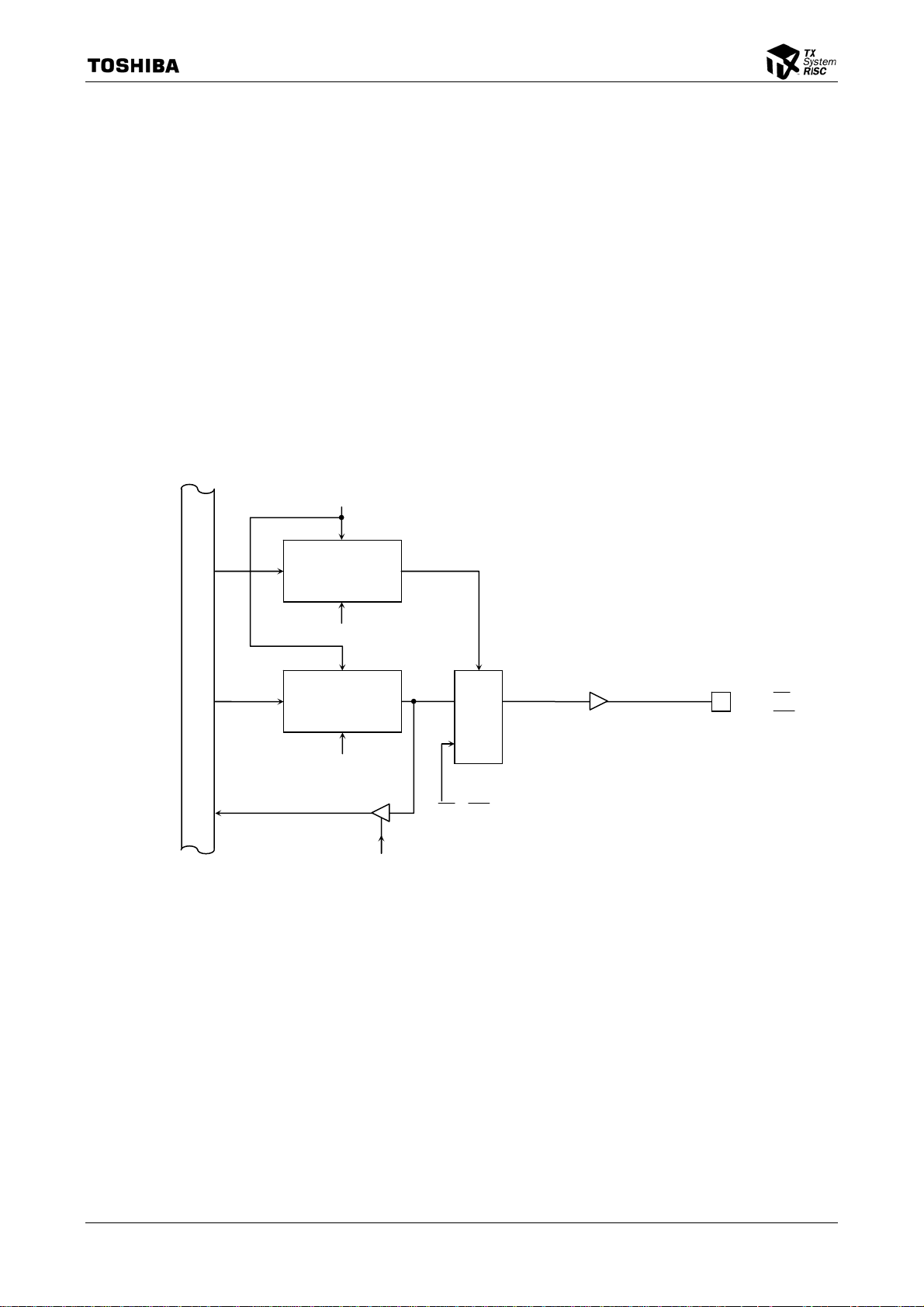
3.5.4 Port 3 (P30-P37)
Port 3 is an 8-bit general-purpose input/output port whose bits can each be set independently for input
or output, with the exception that P30 and P31 are output-only. The control register P3CR and function
register P3FC are used to set the port for input or output. A reset sets b
latch to 1. Bits P32 to P36 are set to 1 by a reset if RSTPUP is High or cleared to 0 if RSTPUP is Low.
All bits of P3CR (bits 0 and 1 not used) and P3FC (bits 3 and 7 not used) are cleared to 0 by a reset, with
P30 and P3
(if RSTPUP is High) or disabled (if RSTPUP is Low). P37 is placed in input mode with a pull-up resistor
enable
d regardless of the value of RSTPUP.
In addition to functioning as a general-purpose input/output port, this port can also input and output
the CPU's control and status signals. The RD strobe is output only when an external address area is being
accessed while the P30 pi
when an external address area is being accessed while the P31 pin is set for WR output (<P31F> = 1).
P32 and P36 have their pull-up resistors enabled when BUSAK = 0 while <P3xFC> = 1.
Internal Data Bus
TMP1942CY/CZ
its P30, P31 and P37 of the output
1 outputting a High signal and P32 to P36 placed in input mode with pull-up resistors enabled
n is set for RD output (<P30F> = 1). Similarly, the WR strobe is output only
Reset
Function Control
(bitwise)
Write to P3FC
S
Output Latch
Write to P3
Read P3
S
A
Selector
B
RD , WR
Output Buffer
P30 (
P31 (
RD )
WR )
Figure 0.7 Port 3 (P30, P31)
TMP1942CY/CZ-75
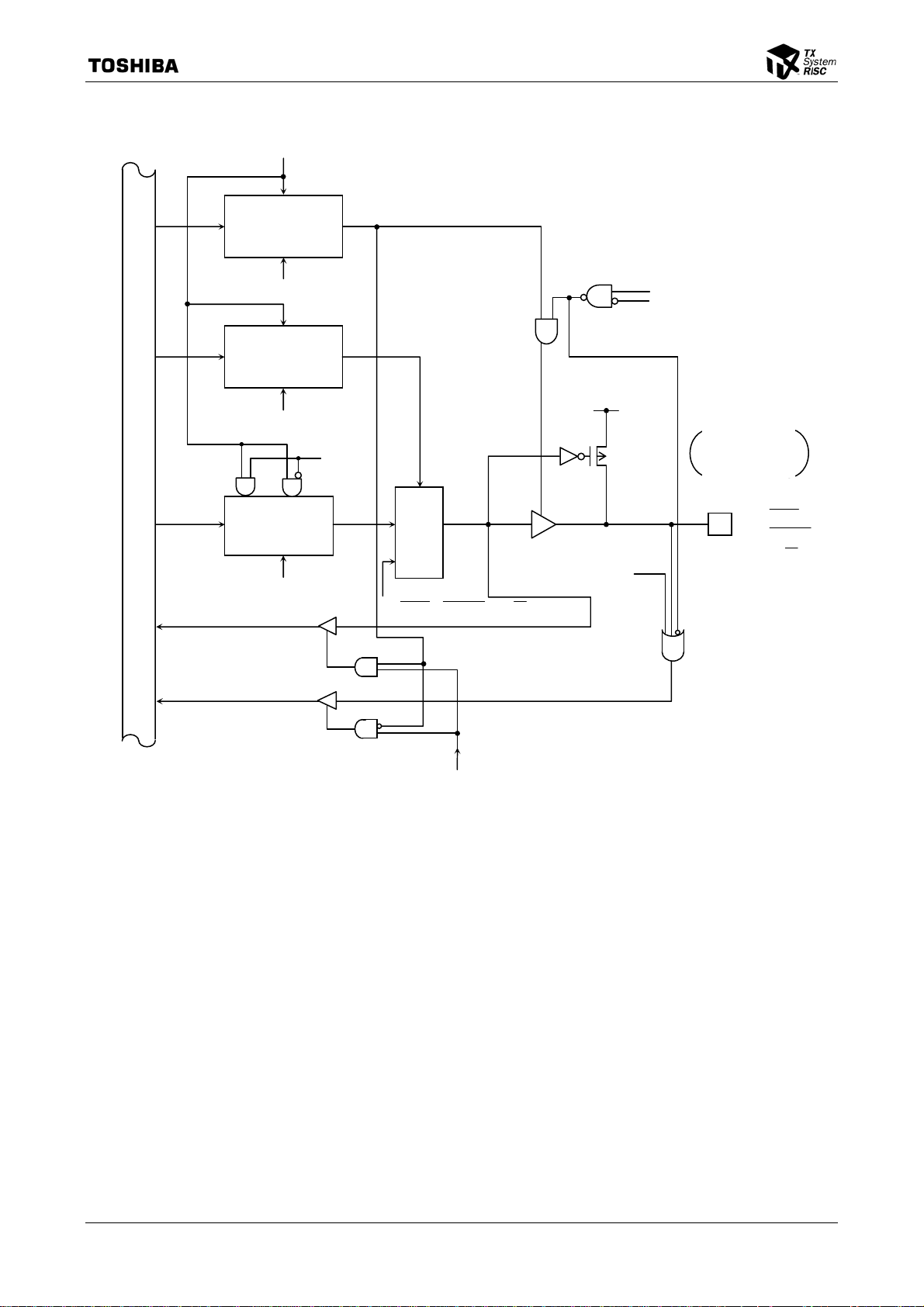
TMP1942CY/CZ
Reset
Direction Control
(bitwise)
Write to P3CR
STOP
DRIVE
Function Control
(bitwise)
InternalDataBus
Write to P3FC
S R
Output Latch
Write to P3
RSTPUP
S
A
Selector
B
HWR , BUSAK , W/R
Output Buffer
P-ch
Reset
Programmable
Pull-up Resistor
P32 (
HWR )
P35 (
BUSAK )
P36 (
W/R)
Read P3
Figure 0.8 Port 3 (P32, P35, P36)
TMP1942CY/CZ-76
Reset
TMP1942CY/CZ
Direction Control
(bitwise)
STOP
DRIVE
Write to P3CR
RSTPUP
P-ch
Programmable
Pull-up Resistor
Internal Data Bus
S R
Output Latch
Write to P3
Output Buffer
Reset
P33 (
WAIT )
Internal
WAIT
Reset
Read P3
Direction Control
(bitwise)
STOP
DRIVE
Write to P3CR
Function Control
(bitwise)
Write to P3FC
RSTPUP
P-ch
Programmable
Pull-up Resistor
Internal Data Bus
S R
Output Latch
Write to P3
Output Buffer
Reset
P34 (
BUSRQ )
Internal
BUSRQ
Read P3
Figure 0.9 Port 3 (P33, P34)
TMP1942CY/CZ-77
TMP1942CY/CZ
Reset
Direction Control
(bitwise)
STOP
DRIVE
Internal data bus
Write to P3CR
S
Output Latch
Write to P3
Output Buffer
P-ch
Programmable
Pull-up Resistor
P37 (
DSU
)
Internal
DSU
Read P3
Figure 0.10 Port 3 (P37)
TMP1942CY/CZ-78
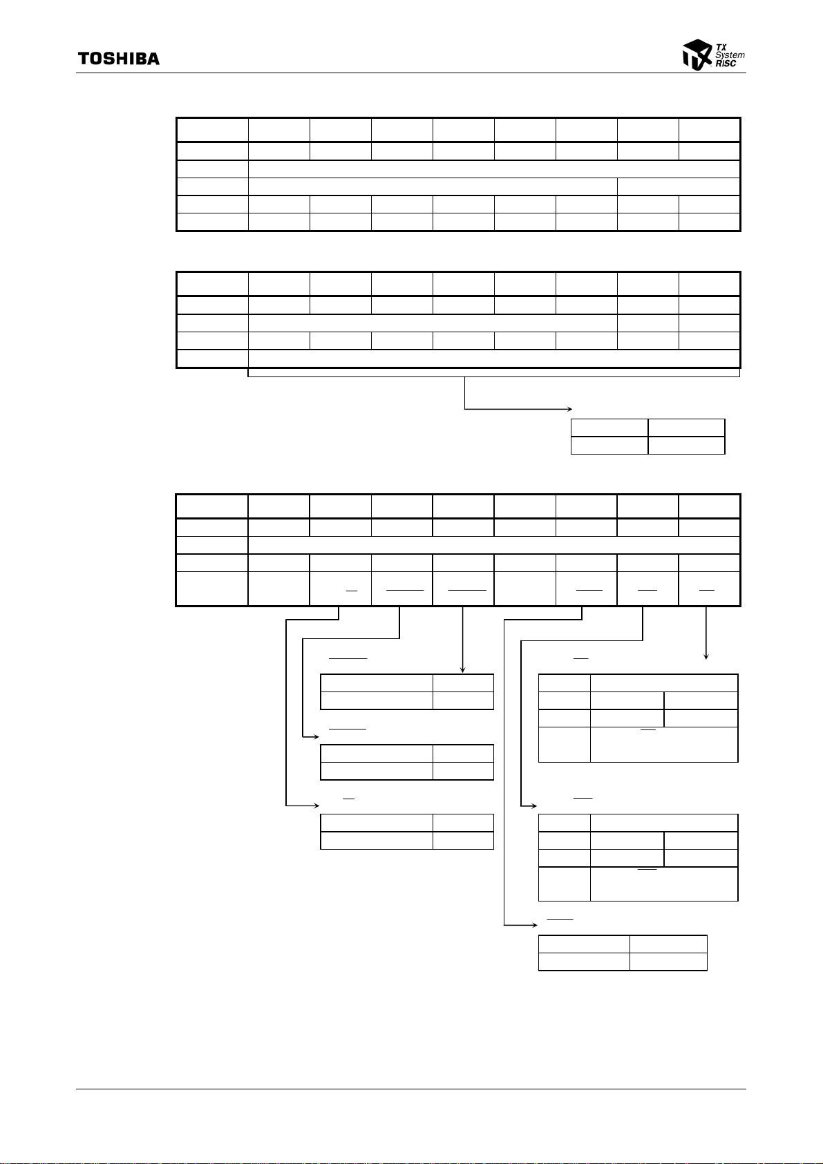
TMP1942CY/CZ
Port 3 Register
7 6 5 4 3 2 1 0
P3 Bit Symbol P37 P36 P35 P34 P33 P32 P31 P30
(0xFFFF_F018) Read/Write R/W
After Reset Input Mode Output Mode
RSTPUP = 1 1 (Pull-UP) 1 (Pull-UP) 1 (Pull-UP) 1 (Pull-UP) 1 (Pull-UP) 1 (Pull-UP) 1 1
RSTPUP = 0 1 (Pull-UP) 0 0 0 0 0 1 1
Port 3 Control Register
7 6 5 4 3 2 1 0
P3CR Bit Symbol P37C P36C P35C P34C P33C P32C ⎯ ⎯
(0xFFFF_F01A) Read/Write W ⎯ ⎯
After Reset 0 0 0 0 0 0 ⎯ ⎯
Function 0: IN 1: OUT
Input/output settings for port 3
0 Input
1 Output
Port 3 Function Register
7 6 5 4 3 2 1 0
P3FC Bit Symbol ⎯ P36F P35F P34F ⎯ P32F P31F P30F
(0xFFFF_F01B) Read/Write W
After Reset ⎯ 0 0 0 ⎯ 0 0 0
P3FC<P34F> 1 <P30>
P3CR<P34C> 0 <P30F> 0 1
0 Outputs 0. Outputs 1.
BUSAK settings 1
P3FC<P35F> 1
P3CR<P35C> 1
W/R settings P31 (WR) function settings
P3FC<P36F> 1 <P31>
P3CR<P36C> 1 <P31F> 0 1
0 Outputs 0. Outputs 1.
1
P3FC<P32F> 1
P3CR<P32C> 1
Function 0: PORT
1:
BUSRQ
0: PORT
W/R
1: BUSAK
settings P30 (RD) function settings
0: PORT
1: BUSRQ
0: PORT
HWR
1:
HWR
settings
0: PORT
1: WR
Outputs
external access.
Outputs
during external access.
RD only during
WR WR only
0: PORT
1: RD
Figure 0.11 Registers Related to Port 3
TMP1942CY/CZ-79

3.5.5 Port 4 (P40-P44)
Port 4 is a 5-bit general-purpose input/output port whose bits can each be set independently for input
or output. The control register P4CR and function register P4FC are used to set the port for input or
output. Bits P41 to P44 of the output latch register are set to 1 by a reset if RSTPUP is Hi
0 if RSTPUP is Low. Bit P44 of the output latch register is set to 1 regardless of the value of RSTPUP.
All bits of P4CR and P4FC are cleared to 0 by a reset, with P40 to P43 pla
resistors enabled (if RSTPUP is High) or disabled (if RSTPUP is Low). P44 is placed in input mode with
a pull-up resistor disabled regardless of the value of RSTPUP.
In addition to functioning as a general-purpose input/output port, P40-P4
select signals (CS0-CS3), and P44 functions as the SCOUT pin, outputting the system clock.
Internal Data Bus
Reset
Direction Control
(bitwise)
Write to P4CR
Function Control
(bitwise)
Write to P4FC
S R
Output Latch
Write to P4
RSTPUP
S
A
Selector
B
CS0 , CS1, CS2, CS3
Read P4
Output Latch
TMP1942CY/CZ
gh or cleared to
ced in input mode with pull-up
3 can also output the chip
STOP
DRIVE
P-ch
Reset
Programmable
Pull-up Resistor
P40 (
P41 (
P42 (
P43 (
CS0
CS1)
CS2 )
CS3
)
)
Figure 0.12 Port 4 (P40-P43)
TMP1942CY/CZ-80
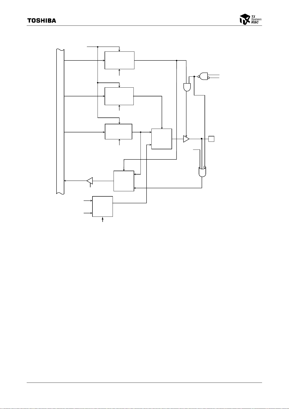
TMP1942CY/CZ
Reset
R
Direction Control
(bitwise)
Write to P4CR
R
Function Control
(bitwise)
STOP
DRIVE
Write to P4FC
Internal data bus
S
Output Latch
Write to P4
SBA
Selector
Y
Reset
P44 (SCOUT)
f
SYS
clock
fs clock
Read P4
A
Selector
B
S
Y
Selector
Y
S
B
A
SYSCR3 <SCOSEL>
Figure 0.13 Port 4 (P44)
TMP1942CY/CZ-81
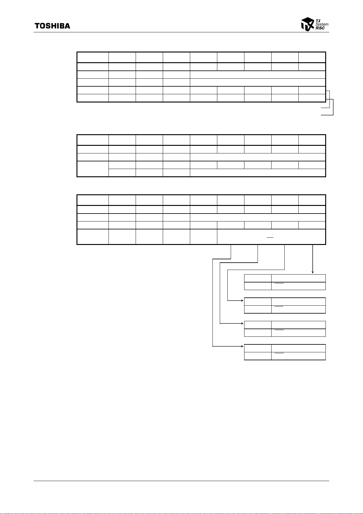
TMP1942CY/CZ
Port 4 Register
7 6 5 4 3 2 1 0
P4 Bit Symbol ⎯ ⎯ ⎯ P44 P43 P42 P41 P40
(0xFFFF_F01E) Read/Write ⎯ ⎯ ⎯ R/W
After Reset ⎯ ⎯ ⎯ Input mode
RSTPUP=1 1 1 (Pull-Up) 1 (Pull-Up) 1 (Pull-Up) 1 (Pull-Up)
RSTPUP=0 1 0 0 0 0
RSTPUp = 1
RSTPUp
= 0
Port 4 Control Register
7 6 5 4 3 2 1 0
P4CR Bit Symbol ⎯ ⎯ ⎯ P44C P43C P42C P41C P40C
(0xFFFF_F020) Read/Write ⎯ ⎯ ⎯ W
After Reset ⎯ ⎯ ⎯ 0 0 0 0 0
0: IN 1: OUT
Port 4 Function Register
7 6 5 4 3 2 1 0
P4FC Bit Symbol ⎯ ⎯ ⎯ P44F P43F P42F P41F P40F
(0xFFFF_F021) Read/Write ⎯ ⎯ ⎯ W
After Reset ⎯ ⎯ ⎯ 0 0 0 0 0
Function 0: PORT
0 PORT (P40)
1 CS0
0 PORT (P41)
1 CS1
0 PORT (P42)
1 CS2
0 PORT (P43)
1 CS3
0: PORT
1: SCOUT 1: CS
Figure 0.14 Registers Related to Port 4
TMP1942CY/CZ-82

3.5.6 Port 5 (P50-P57)
Port 5 is an 8-bit input-only port, and is shared with the A/D converter's analog input pins. P57 also
functions as the A/D converter's A/D trigger input pin.
Internal Data Bus
Function Control
Write P5FC
Internal Data Bus
ADTRG
(P57 Only)
Read Port 5
Read A/D
Read Port 5
Read A/D
Conversion
Result Register
Conversion
Result Register
A/D Converter
A/D Converter
TMP1942CY/CZ
Channel
Selector
Channel
Selector
Port 5
P50-P56
(AN0-AN7)
Port 5
P57
ADTRG
(AN7)/
Figure 0.15 Port 5 (P50-P57)
TMP1942CY/CZ-83
TMP1942CY/CZ
Port 5 Register
7 6 5 4 3 2 1 0
P5 Bit Symbol P57 P56 P55 P54 P53 P52 P51 P50
(0xFFFF_F040) Read/Write R
After Reset Input mode
Port 5 Function Register
7 6 5 4 3 2 1 0
P5FC Bit Symbol P57F ⎯ ⎯ ⎯ ⎯ ⎯ ⎯ ⎯
(0xFFFF_F043) Read/Write W ⎯
After Reset 0 ⎯ ⎯ ⎯ ⎯ ⎯ ⎯ ⎯
Function 0: Port or
A/D input
1:
ADTRG
Figure 0.16 Port 5 (P50-P57)
Note 1: Use A/D converter mode register ADMOD4 to select A/D converter input channels and to enable
A/D trigger input for P57.
Note 2: To use
ADMOD4. To stop using
ADTRG, first set <P57F> to 1 and then enable trigger input in A/D converter mode register
ADTRG, first disable trigger input in ADMOD4 and then clear <P57F> to 0
(port).
TMP1942CY/CZ-84

3.5.7 Port 6 (P60-P67)
Port 6 is an 8-bit input-only port, and is shared with the A/D converter's analog input pins and key
input pins. A reset clears P6FC to 0, placing port 6 in A/D or port input mode. Writing a 1 to a bit of
P6FC enables the corresponding pi
enabled only for those pins for which KWUPCNT<PE> is set to 1 in the key on wake-up circuit and key
input is enabled in KWUPSTn. For details, refer to the description of th
Internal Data Bus
Function Control
Write P6FC
KEY0-7
Read Port 6
Read A/D
n to be used as a key input pin. Port 6 has pull-up resistors, which are
Conversion
Result Register
fs
A/D Converter
DPE
A
TG
B
Y
Selector
TMP1942CY/CZ
e key on wake-up function.
Channel
Selector
KEYmEN
PE
Port 6
P60-67
(AN8-15)/
KEY0-7
Figure 0.17 Port 6 (P60-P67)
Port 6 Register
7 6 5 4 3 2 1 0
P6 Bit Symbol P67 P66 P65 P64 P63 P62 P61 P60
(0xFFFF_F041) Read/Write R
After Reset Input mode
Port 6 Function Register
7 6 5 4 3 2 1 0
P6FC Bit Symbol P67F P66F P65F P64F P63F P62F P61F P60F
(0xFFFF_F045) Read/Write W
After Reset 0
Function 0: Port or A/D input 1: Key input
Figure 0.18 Registers Related to Port 6
TMP1942CY/CZ-85
3.5.8 Port 9 (P90-P97)
Port 9 is an 8-bit general-purpose input/output port whose bits can each be set independently for input
or output. The control register P9CR is used to set the port for input or output. A reset clears P9CR to 0,
putting port 9 in input mode. In addition to f
also function as various input/output pins: P90 and P91 function as key input, P92 to P94 and P97 as
16-bit timer output, and P95 and P96 as 16-bit timer input. These functions are enabled by setting th
corresponding bits of P9FC to 1.
A reset clears P9CR and P9FC to 0, placing port 9 in input mode. Pins P90 and P91 have pull-up
resistors, which are enabled only for those pins for which KWUPCNT<PE> is set to 1 in the key on
wake-up circui
wake-up function. When a pin is functioning as a port pin, its pull-up resistor is disabled.
When the DSU is enabled, port 9 functions as a DSU interface regardless of th
P9FC, so that the pins cannot be used as general-purpose port pins or peripheral function pins as
described above.
Internal Data Bus
TMP1942CY/CZ
unctioning as an input/output port, the pins of this port can
t and key input is enabled in KWUPSTn. For details, refer to the description of the key on
e settings in P9CR and
Function Control
Reset
Write to P9FC
Direction Control
(bitwise)
STOP
DRIVE
Write to P9CR
S
Output Latch
Write to P9
KEY8, 9
fs
TG
Output Buffer
Read P9
DPE
A
Y
Selector
B
KEYmEN
PE
P90 (KEY8)
P91 (KEY9)
Reset
e
Figure 0.19 Port 9 (P90, P91)
TMP1942CY/CZ-86
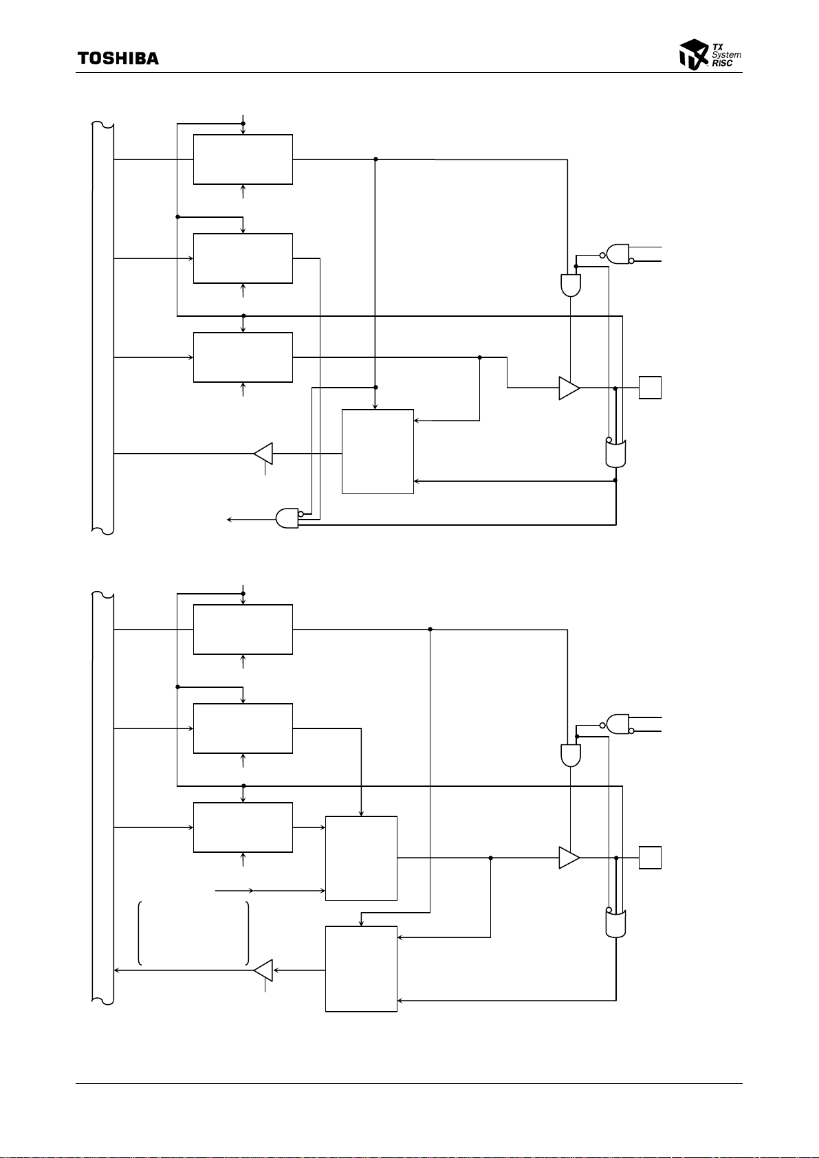
TMP1942CY/CZ
Reset
Direction Control
(bitwise)
Write to P9CR
Function Control
(bitwise)
STOP
DRIVE
Write to P9FC
Internal DataBus
S
Output Latch
Write to P9
S
Selector
P95 (TB7IN0)
P96 (TB7IN1)
B
Read P9
A
TB7IN0, 1
Reset
Direction Control
(bitwise)
Write to P9CR
Function Control
(bitwise)
STOP
DRIVE
Write to P9FC
S
Internal Data Bus
Timer F/F Output
TB4OUT: Timer B4
TB5OUT: Timer B5
TB6OUT: Timer B6
TB7OUT: Timer B7
Output Latch
Write to P9
Read P9
A S
Selector
B
Selector
S B
P92 (TB4OUT)
P93 (TB5OUT)
P94 (TB6OUT)
P97 (TB7OUT)
A
Figure 0.20 Port 9 (P92-P97)
TMP1942CY/CZ-87

TMP1942CY/CZ
Port 9 Register
P9
(0xFFFF_F04C)
7 6 5 4 3 2 1 0
Bit Symbol P97 P96 P95 P94 P93 P92 P91 P90
Read/Write R/W
After Reset Input mode (output latch register set to 1)
Port 9 Control Register
P9CR
(0xFFFF_F04E)
7 6 5 4 3 2 1 0
Bit Symbol P97C P96C P95C P94C P93C P92C P91C P90C
Read/Write W
After Reset 0 0 0 0 0 0 0 0
Function 0: IN 1: OUT
Port 9 Function Register
P9FC
(0xFFFF_F04F)
7 6 5 4 3 2 1 0
Bit Symbol P97F P96F P95F P94F P93F P92F P91F P90F
Read/Write W
After Reset 0 0 0 0 0 0 0 0
Function 0: PORT
1: TB7OUT
0: PORT
1: TB7IN1
0: PORT
1: TB7IN0
0: PORT
1: TB6OUT
Function
Select KEY8 input 1 0 P90
Select KEY9 input 1 0 P91
Select TB4OUT output 1 1 P92
Select TB5OUT output 1 1 P93
Select TB6OUT output 1 1 P94
Select TB7IN0 input 1 0 P95
Select TB7IN1 input 1 0 P96
Select TB7OUT output 1 1 P97
Corresponding
P9FC Bit
Input/output settings for port 9
0: PORT
1: TB5OUT
0: PORT
1: TB4OUT
Corresponding
P9CR Bit
0 Input
1 Output
0: PORT
1: KEY9
0: PORT
1: KEY8
Port Used
Figure 0.21 Registers Related to Port 9
TMP1942CY/CZ-88
3.5
A
A
3.5.9 Port A (P A0-P A7)
Port A is an 8-bit general-purpose input/output port whose bits can each b e set i n dependently for input
or output. The control register PACR is used to set the port for input or output. A reset clears PACR to 0,
putting port A in input mode. In addition to functioning as an input/output port, the pins of this port can
also function as various input/output pins: PA 0 , PA1 , PA3 and PA4 function as 16-bit timer input or
external interrupt input, PA2 and PA5 as 16-bit timer output, PA6 as 8-bit timer output, and PA7 as 8-bit
timer input or key input. These functions are enabled by setting the corresponding bits of PAFC to 1.
A reset clears PACR and PAFC to 0, placing port A in input m ode. PA7 has a pull-up resistor, which is
enabled only when KWUPCNT<PE> is set to 1 in the key on wake-up circuit and key input is enabled by
setting 1 in PAFC. When the pin is functioning as a port pin, its pull-up resistor is disabled.
Internal Data Bus
Timer F/F Output
TB0OUT
TB1OUT
TA1OUT
Reset
Direction Control
(bitwise)
Write to PACR
Function Control
(bitwise)
Write to PAFC
S
Output Latch
Write to PA
Read PA
Selector
B
Selector
TMP1942CY/CZ
STOP
DRIVE
S
PA2 (TB0OUT)
PA5 (TB1OUT)
PA6 (TA1OUT)
S
B
Figure 3.5.21 Port A (PA2, PA5, PA6)
TMP1942CY/CZ-89

A
Reset
TMP1942CY/CZ
Direction Control
(bitwise)
Write to PACR
Function Control
(bitwise)
STOP
DRIVE
Write to PAFC
Internal Data Bus
S
Output Latch
PA0 (TB0IN0/INT3)
PA1 (TB0IN1/INT4)
Write to PA
TB0IN0, TB0IN1
INT3, INT4
Read PA
S
Selector
B
A
Reset
Direction Control
(bitwise)
Write to PACR
Function Control
(bitwise)
STOP
DRIVE
Write to PAFC
Internal data bus
TA0IN
KEYA
S
Output Latch
Write to PA
Read PA
S
Selector
B
Reset
PA7 (TA0IN/KEYA)
DPE
Selector
B
Y
fs
TG
KEYmEN
PE
Figure 3.5.22 Port A (PA0, PA1, PA7)
TMP1942CY/CZ-90
TMP1942CY/CZ
Reset
Direction Control
(bitwise)
Write to PACR
Function Control
(bitwise)
STOP
DRIVE
Write to PAFC
Internal data bus
S
Output Latch
PA3 (TB1IN0/INT5)
PA4 (TB1IN1/INT6)
Write to PA
TB1IN0, TB1IN1
INT5, INT6
Read PA
S
Selector
B
A
Figure 3.5.23 Port A (PA3, PA4)
TMP1942CY/CZ-91
TMP1942CY/CZ
Port A Register
7 6 5 4 3 2 1 0
PA Bit Symbol PA7 PA6 PA5 PA4 PA3 PA2 PA1 PA0
(0xFFFF_F050) Read/Write R/W
After Reset Input mode (output latch register set to 1)
1 1 1 1 1 1 1 1
Port A Control Register
7 6 5 4 3 2 1 0
PACR Bit Symbol PA7C PA6C PA5C PA4C PA3C PA2C PA1C PA0C
(0xFFFF_F052) Read/Write W
After Reset 0 0 0 0 0 0 0 0
Function 0: IN 1: OUT
Input/output settings for port A
0
1 Output
Port A Function Register
Input
7 6 5 4 3 2 1 0
PAFC Bit Symbol PA7F PA6F PA5F PA4F PA3F PA2F PA1F PA0F
(0xFFFF_F053) Read/Write W
After Reset 0 0 0 0 0 0 0 0
Function 0: PORT
1: TA0IN
KEYA
0: PORT
1: TA1OUT
0: PORT
1: TB1OUT
0: PORT
1: TB1IN1
INT6
0: PORT
1: TB1INT0
INT5
0: PORT
1: TB0OUT
0: PORT
1: TB0IN1
INT4
0: PORT
1: TB0IN0
INT3
Function
Select TB0IN0 input 1 0
Select INT3 input 1 (*1) 0
Select TB0IN1 input 1 0
Select INT4 input 1 (*1) 0
Select TB0OUT output 1 1 PA2
Select TB1IN0 input 1 0
Select INT5 input Need not be set 0
Select TB1IN1 input 1 0
Select INT6 input Need not be set 0
Select TB1OUT output 1 1 PA5
Select TA1OUT output 1 1 PA6
Select TA0IN input 1 0
Select KEYA input 1 0
Corresponding
PAFC Bit
Corresponding
PACR Bit
Port Used
PA0
PA1
PA3
PA4
PA7
(*1) Set this bit when using the pin for a STOP mode termination interrupt with
SYSCR<DRVE> set to 0. Otherwise, the bit need not be set.
Note: For a pin to which two input functions are assigned in addition to the port function, use
the control register for each function module to specify which function is used.
Figure 3.5.24 Registers Related to Port A
TMP1942CY/CZ-92

A
3.5.10 Port B (PB0-PB7)
Port B is an 8-bit general-purpose input/output port whose bits can each be set independently for input
or output. The control register PBCR is used to set the port for input or output. A reset clears PBCR to 0,
putting port B in input mode. In addition to functioning as an input/output port, the pins of this port can
also function as various input/output pins: PB0, PB1, PB3 and PB4 function as 16-bit timer input or
external interrupt input, PB2 and PB5 as 16-bit timer input or output, PB7 as 8-bit timer input, interrupt
input or key input. These functions are enabled by setting the corresponding bits of PBFC to 1.
A reset clears PBCR and PBFC to 0, placing port B i n inp ut m ode. PB 7 has a pull-up re sistor, which is
enabled only when KWUPCNT<PE> is set to 1 in the key on wake-up circuit and key input is enabled in
KWUPSTn. For details, refer to the description of the key on wake-up function. When the pin is
functioning as a port pin, its pull-up resistor is disabled.
Internal Data Bus
Timer F/F Output
TB2OUT
TB3OUT
Reset
Direction Control
(bitwise)
Write to PBCR
Function Control
(bitwise)
Write to PBFC
S
Output Latch
Write to P7
Read to P7
TB4IN0
TB4IN1
Selector
B
Selector
TMP1942CY/CZ
STOP
DRIVE
S
PB2 (TB2OUT/TB4IN0)
S
B
A
PB5 (TB3OUT/TB4IN1)
Figure 3.5.25 Port B (PB2, PB5)
TMP1942CY/CZ-93
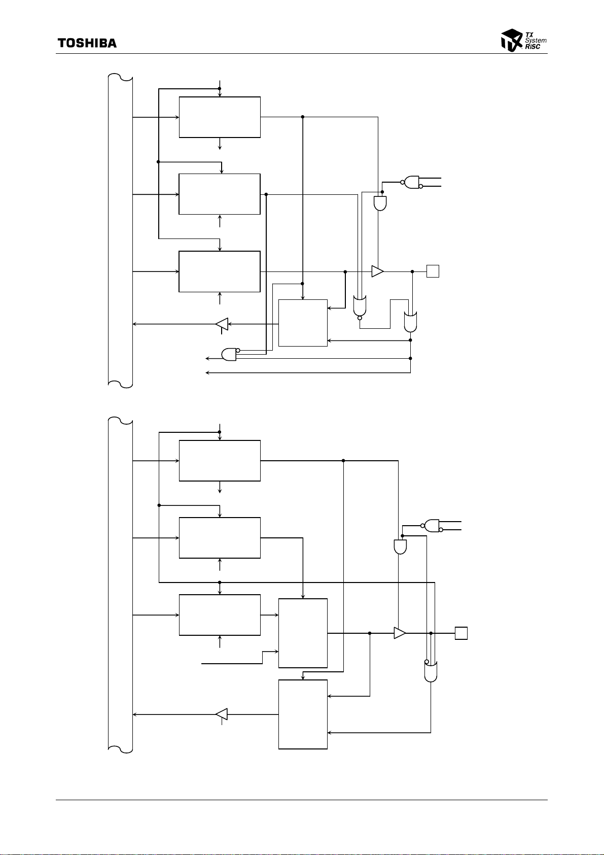
TMP1942CY/CZ
Reset
Direction Control
(bitwise)
Write to PBCR
Function Control
(bitwise)
STOP
DRIVE
Write to PBFC
Internal data bus
TB2IN0, 1
TB3IN0, 1
INTB, C, D, E
S
Output Latch
Write to PB
Read PB
S
Selector
PB0 (TB2IN0/INTB)
PB1 (TB2IN1/INTC)
PB3 (TB3IN0/INTD)
PB4 (TB3IN1/INTE)
B
A
Reset
Direction Control
(bitwise)
Write to PBCR
Function Control
(bitwise)
STOP
DRIVE
Write to PBFC
Internal data bus
Timer F/F output
(TA3OUT: Timer A3)
S
Output Latch
Write to PB
Read PB
A
Selector
B
Selector
S
S
B
A
PB6 (TA3OUT)
Figure 3.5.26 Port B (PB0, PB1, PB3, PB4, PB6)
TMP1942CY/CZ-94

TMP1942CY/CZ
Reset
Direction Control
(bitwise)
Write to PBCR
STOP
DRIVE
Function Control
(bitwise)
Write to PBFC
Internal Data Bus
S
Output Latch
PB7 (TA2IN/INT7/KEYB)
S
Write to PB
Selector
Read PB
TA2IN
INT7
KEYB
DPE
B
A
fs
TG
B
Y
Selector
KEYmEN
PE
Figure 3.5.27 Port B (PB7)
TMP1942CY/CZ-95
TMP1942CY/CZ
Port B Register
7 6 5 4 3 2 1 0
PB Bit Symbol PB7 PB6 PB5 PB4 PB3 PB2 PB1 PB0
(0xFFFF_F051) Read/Write R/W
After Reset Input mode (output latch register set to 1)
Port B Control Register
7 6 5 4 3 2 1 0
PBCR Bit Symbol PB7C PB6C PB5C PB4C PB3C PB2C PB1C PB0C
(0xFFFF_F054) Read/Write W
After Reset 0 0 0 0 0 0 0 0
Function 0: IN 1: OUT
Input/output settings for port B
0
1 Output
Port B Function Register
7 6 5 4 3 2 1 0
PBFC Bit Symbol PB7F PB6F PB5F PB4F PB3F PB2F PB1F PB0F
(0xFFFF_F055) Read/Write W
After Reset 0 0 0 0 0 0 0 0
Function 0:PORT
1:TA2IN
INT7
KEYB
0: PORT
1: TA3OUT
0: PORT
1: TB3OUT
TB4IN1
0: PORT
1: INTE
TB3IN1
0: PORT
1: INTD
TB3IN0
0: PORT
1: TB2OUT
TB4IN0
Function
Select TB2IN0 input 1 0
Select INTB input 1 (*1) 0
Select TB2IN1 input 1 0
Select INTC input 1 (*1) 0
Select TB2OUT output 1 1
Select TB4IN0 input 0 1
Select TB3IN0 input 1 0
Select INTD input 1 (*1) 0
Select TB3IN1 input 1 0
Select INTE input 1 (*1) 0
Select TB3OUT output 1 1
Select TB4IN1 input 0 1
Select TA3OUT output 1 1 PB6
Select TA2IN input 1 0
Select INT7 input 1 0
Select KEYB input 1 0
Corresponding
PBFC Bit
Corresponding
PBCR Bit
Input
0: PORT
1: INTC
TB2IN1
Port Used
PB0
PB1
PB2
PB3
PB4
PB5
PB7
0: PORT
1: INTB
TB2IN0
(*1) Set this bit when using the pin for a STOP mode termination interrupt with
SYSCR<DRVE> set to 0. Otherwise, the bit need not be set.
Note: For a pin to which two or three input functions are assigned in addition to the port
function, use the control register for each function module to specify which function is
used.
Figure 3.5.28 Registers Related to Port B
TMP1942CY/CZ-96
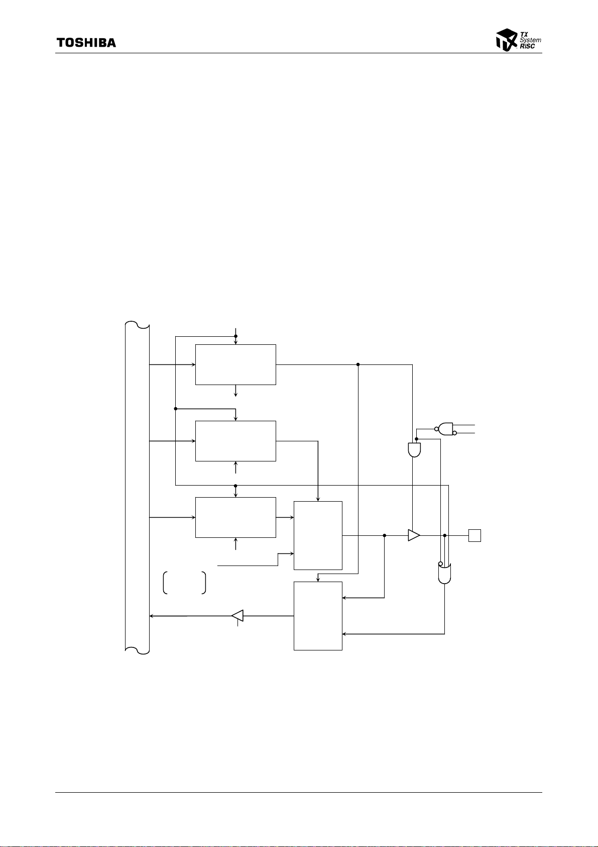
3.5.11 Port C (PC0-PC7)
Port C is an 8-bit general-purpose input/output port whose bits can each be set independently for input
or output. The control register PCCR is used to set the port for input or output. A reset clears PCCR to 0,
putting port C in input mode. In addition to functioning as an input/output port, the pins of this port can
also function as various input/output pins: PC0, PC1 and PC2 function as 8-bit timer input or external
interrupt input, PC3 and PC5 as 8-bit timer output, PC6 as 16-bit timer input or key input, PC4 as 8-bit
timer input, and PC7 as 16-bi t timer input o r 8-bit time r output. These functi ons are enabled by setti ng the
corresponding bits of PCFC to 1.
A reset clears PCCR and PCFC to 0, placing port C i n inp ut m ode. PC 6 has a pull-up re sistor, which is
enabled only when KWUPCNT<PE> is set to 1 in the key on wake-up circuit and key input is enabled in
KWUPSTn. For details, refer to the description of the key on wake-up function. When the pin is
functioning as a port pin, its pull-up resistor is disabled.
Port C becomes a 5 V input/output port when 5 V is supplied to its dedicated power supply pin
DVCC52. It becomes a VCC-based (3 V) port when VCC is supplied to DVCC52.
Internal data bus
Timer F/F Output
TA5OUT
TA7OUT
Reset
Direction Control
(bitwise)
Write to PCCR
Function Control
(bitwise)
Write to PCFC
S
Output Latch
Write to PC
Read PC
A
Selector
B
Selector
TMP1942CY/CZ
STOP
DRIVE
S
PC3 (TA5OUT)
PC5 (TA7OUT)
S
B
A
Figure 3.5.29 Port C (PC3, PC5)
TMP1942CY/CZ-97
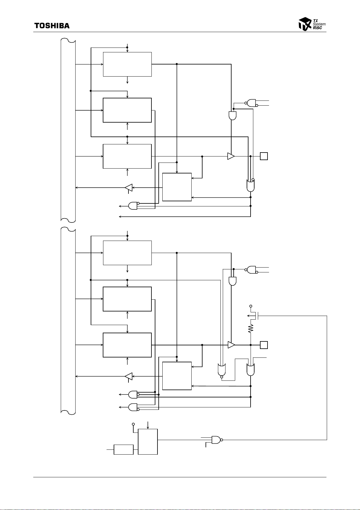
Reset
TMP1942CY/CZ
Direction Control
(bitwise)
Write to PCCR
Function Control
(bitwise)
STOP
DRIVE
Write to PCFC
Internal Data Bus
TA4IN, TA6IN
TA8IN
INT8, 9, A
S
Output Latch
Write to PC
Read PC
Reset
S
Selector
PC0 (TA4IN/INT8)
PC1 (TA6IN/INT9)
PC2 (TA8IN/INTA)
B
A
Direction Control
(bitwise)
Write to PCCR
Function Control
(bitwise)
STOP
DRIVE
Write to PCFC
Internal Data Bus
TB8IN0
S
Output Latch
Write to PC
Read PC
S
Selector
PC6 (TB8IN0/IN0/KEYC)
Reset
B
A
KEYC
fs
TG
DPE
A
B
Y
Selector
KEYmEN
PE
Figure 3.5.30 Port C (PC0, PC1, PC2, PC6)
TMP1942CY/CZ-98

A
A
A
Reset
TMP1942CY/CZ
Direction Control
(bitwise)
Write to PCCR
Function Control
(bitwise)
STOP
DRIVE
Write to PCFC
Internal Data Bus
Timer F/F Output
TA9OUT
S
Output Latch
Write to PC
Read PC
Selector
B
Selector
S
S
B
PC7 (TB8IN1/TA9OUT)
TB8IN1
Reset
Direction Control
(bitwise)
Write to PCCR
Function Control
(bitwise)
STOP
DRIVE
Internal Data Bus
Write to PCFC
S
Output Latch
PC4 (TAIN)
Write to PC
Read PC
S
Selector
B
TAAIN
Figure 3.5.31 Port C (PC7, PC4)
TMP1942CY/CZ-99
 Loading...