

现货库存、技术资料、百科信息、热点资讯,精彩尽在鼎好!
TLP629,TLP629−2,TLP629−4
TOSHIBA Photocoupler GaAs Ired & Photo−Transistor
TLP629,TLP629−2,TLP629−4
Telecommunication
Office Machine
Telephone Use Equipment
The TOSHIBA TLP629, −2, and −4 consists of a photo−transistor
optically coupled to a gallium arsenide infrared emitting diode.
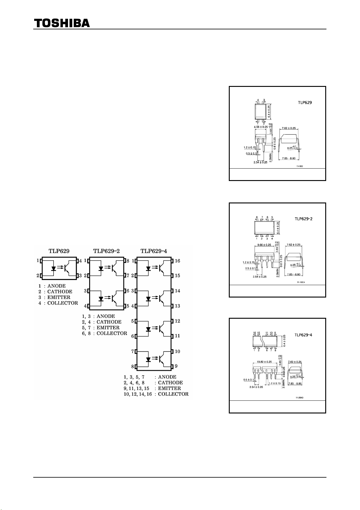
The TLP629−2 offers two isolated channels in an eight lead plastic DIP,
while the TLP629−4 provides four isolated channels in a sixteen plastic
DIP. This is suitable for application of DC input current up to 150mA.
• I
maximum rating: 150mA
F
• Collector−emitter voltage: 55V (min.)
• Current transfer ratio: 25% (min.) (I
• Isolation voltage: 5000V
• UL recognized: UL1577, file no. E67349
• BSI approved: BS EN60065:2002, certificate no.7426
BS EN60950-1:2002, certificate no.7427
Pin Configurations
(min.)
rms
(top view)
=20mA)
F
Weight: 0.26 g
Unit in mm
TOSHIBA 11−5B2
TOSHIBA 11−10C4
Weight: 0.54 g
TOSHIBA 11−20A3
Weight: 1.1 g
1
2007-10-01
TLP629,TLP629−2,TLP629−4
Absolute Maximum Ratings
Characteristic Symbol
Forward current IF 150 mA
Forward current derating ΔIF / °C −1.5 (Ta ≥ 25°C) mA / °C
Pulse forward current IFP 1 (100μs pulse, 100pps) A
LED
Reverse voltage VR 5 V
Junction temperature Tj 125 °C
Collector−emitter voltage V
Emitter−collector voltage V
Collector current IC 80 mA
Collector power dissipation
(1 circuit)
Detector
Collector power dissipation derating
(1 circuit, Ta ≥ 25°C)
Junction temperature Tj 125 °C
Storage temperature range T
Operating temperature range T
Lead soldering temperature T
Total package power dissipation PT 250 200 mW
Total package power dissipation derating
(Ta≥25°C)
Isolation voltage (Note 1) BVS 5000 (AC, 1min., RH ≤ 60%)
(Ta = 25°C)
CEO
ECO
150 100 mW
P
C
/ °C −1.5 −1.0 mW / °C
ΔP
C
−55~125 °C
stg
−55~100 °C
opr
260 (10s) °C
sol
/ °C −2.5 2.0 mW / °C
ΔP
T
Rating
TLP629 TLP629−2,4
55 V
7 V
Unit
V
rms
Note: Using continuously under heavy loads (e.g. the application of high temperature/current/voltage and the
significant change in temperature, etc.) may cause this product to decrease in the reliability significantly even
if the operating conditions (i.e. operating temperature/current/voltage, etc.) are within the absolute maximum
ratings.
Please design the appropriate reliability upon reviewing the Toshiba Semiconductor Reliability Handbook
(“Handling Precautions”/“Derating Concept and Methods”) and individual reliability data (i.e. reliability test
report and estimated failure rate, etc).
(Note 1) Device considered a two terminal: LED side pins shorted together, and detector side pins shorted together.
Recommended Operating Conditions
Characteristics Symbol Min. Typ. Max. Unit
Supply voltage VCC ― 5 24 V
Forward current IF ― 20 120 mA
Collector current IC ― 1 10 mA
Operating temperature T
Note: Recommended operating conditions are given as a design guideline to obtain expected performance of the
device. Additionally, each item is an independent guideline respectively. In developing designs using this
product, please confirm specified characteristics shown in this document.
−25
opr
― 85 °C
2
2007-10-01
TLP629,TLP629−2,TLP629−4
Individual Electrical Characteristics
Characteristic Symbol Test Condition Min. Typ. Max. Unit
Forward voltage VF IF = 100 mA — 1.4 1.7 V
Forward current IF VF = 0.7 V — 2.5 20 μA
LED
Reverse current IR V
Capacitance CT V = 0, f = 1 MHz — 50 — pF
Collector−emitter
breakdown voltage
Emitter−collector
breakdown voltage
Detector
Collector dark current I
Capacitance collector to emitter CCE V = 0, f = 1 MHz — 10 — pF
Coupled Electrical Characteristics
Characteristic Symbol Test Condition MIn. Typ. Max. Unit
Current transfer ratio
Collector−emitter saturation voltage V
Off−state collector current I
Isolation Characteristics
(Ta = 25°C)
V
(BR) CEO
V
(BR) ECO
CEO
(Ta = 25°C)
IC / I
/ I
I
C
(high)
CE (sat)
C(off)
(Ta = 25°C)
R
IC = 0.5 mA 55 — — V
IE = 0.1 mA 7 — — V
VCE = 24 V — 10 100 nA
V
CE
= 5 V — — 10 μA
= 24 V, Ta = 85°C — 2 50 μA
IF = 20 mA, VCE = 1 V 25 — —
F
F
I
= 100 mA, VCE = 1 V 20 — 80
F
IC = 2.4 mA, IF = 20 mA — — 0.4
IC = 2.4 mA, IF = 100 mA — — 0.4
VF = 0.7V, V
= 24 V — 1 1.0 μA
CEO
%
V
Characteristic Symbol Test Condition Min. Typ. Max. Unit
Capacitance input to output C
Isolation resistance R
Isolation voltage BV
VS = 0, f = 1 MHz — 0.8 — pF
S
VS = 500 V 5×10
S
AC, 1 minute 5000 — —
AC, 1 second, in oil — 10000 —
S
DC, 1 minute, in oil — 10000 — Vdc
10 1014
— Ω
V
rms
3
2007-10-01
 Loading...