

查询TC74A23F供应商
Toshiba CMOS Digital Integrated Circuit Silicon Monolithic
TC94A23F
Single-chip CD Processor with Built-in Controller
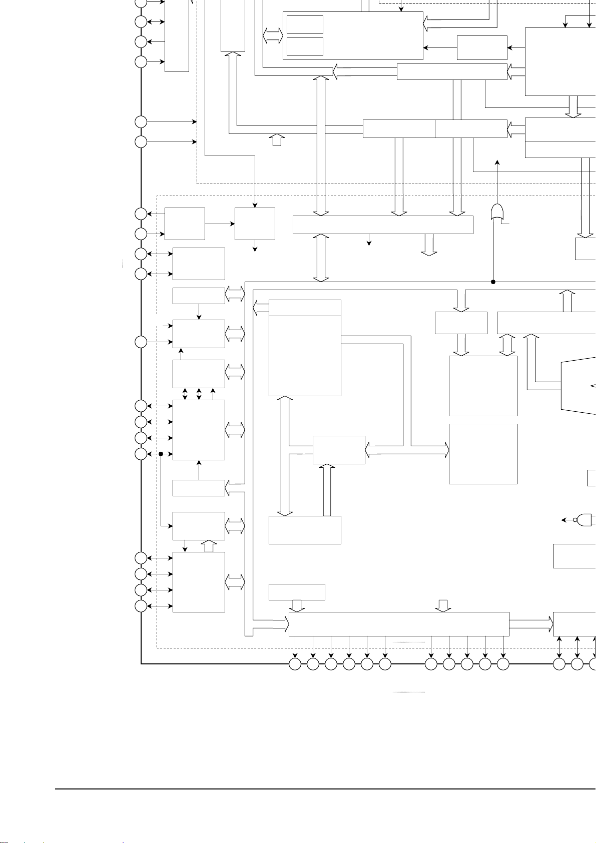
TC94A23F is a single-chip CD processor for digital servo. It
incorporates a 4-bit microcontroller.
The controller features an LCD/LED driver, 4-channel 6-bit AD
converter, 2/3-line serial interface, buzzer, interrupt function, and
8-bit timer/counter. The CPU can select one of three crystal
oscillator operating clocks (16.9344 MHz, 4.5 MHz, and 75 kHz),
facilitating interface with the CD processor.
The CD processor incorporates sync separation protection and
interpolation, EFM decoder, error correction, digital equalizer for
servo, and servo controller. The CD processor also incorporates a
1-bit DA converter. In combination with RF amp TA2153FN or
TA2109F, TC94A23F can very simply configure an
adjustment-free CD player.
Thus, the IC is suitable for CD systems for automobiles and radio-cassette players.
Features
Weight: 1.6 g (typ.)
TC94A23F
· Single-chip CD processor with built-in CMOS LCE/LED driver and 4-bit microcontroller
· Operating voltage: At CD on: V
At CD off: V
· Current dissipation: At CD on: I
At CD off: I
At CD off: I
· Operating temperature range: Ta = -40~85°C
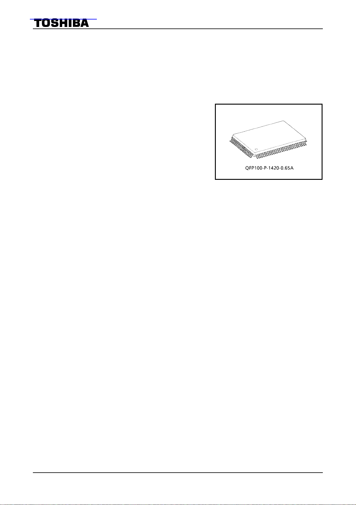
· Package: QFP100-P-1420-0.65A (0.65-mm pitch, 2.7-mm thick)
· One-time PROM version: TC94AP09F
= 4.5 to 5.5 V (typ. 5.0 V)
DD
= 3.0 to 5.5 V (only CPU on)
DD
= 50 mA (typ.)
DD
= 2 mA (with 4.5 MHz crystal oscillator, only CPU on)
DD
= 0.3 mA (with 75 kHz crystal oscillator, only CPU on)
DD
1
2002-02-06

4-bit Microcontroller
· Program memory (ROM): 16-bit ´ 8k-step
· Data memory (RAM): 4-bit ´ 512-word
· Instruction execution time: 1.89/1.78/40 ms (all one-word instructions)
· Crystal oscillator frequency: 16.9344 MHz/4.5 MHz/75 kHz
· Stack level: 8
· AD converter: 6-bit ´ 4-channel
· LCD driver: 1/4 duty, 1/2 or 1/3 bias method, 72 segments max
· LED driver: 4-digit ´ 14-segment (max), also used as LCD driver switched by software
· I/O port: CMOS I/O port: 16
N-channel open drain I/O port: 4 (max)
Output-only port: 4 (max), also used as CD processor pins
Input-only port: 4
· Timer/counter: 8 bit (INTR, instruction cycle, 100/1 kHz selectable as timer clock)
10, 100, or 500 Hz: internal port
2 Hz: Flip-flop port
· Serial interface: Supports 2/3-line method (data length: 4 or 8 bits)
· Buzzer: Four types: 0.75, 1, 1.5, and 3 kHz
Four modes: Continuous, Single-Shot, 10 Hz Intermittent, and 10 Hz Intermittent at 1 Hz Interval)
· Interrupt: 1 external, 3 internal (CD sub-sync, serial interface, 8-bit timer)
· Back-up mode: three types
Clock Stop (crystal oscillator off)
Hardware Wait (crystal oscillator on but CPU in operation)
Software Wait (CPU in intermittent operation)
· Reset function: Power-on reset, built-in supply voltage detector (detection voltage = 2.5 V typ.)
CD Processor
· Reliable sync pattern detection, sync signal protection and interpolation
· Built-in EFM decoder and sub code decoder
· High-correction capability using cross interleave read Solomon code (CIRC) logical equation
C1 correction: dual
C2 correction: quadruple
· Supports variable speeds.
· Jitter absorption capability of ±6 frames
· Built-in 16 KB RAM
· Built-in digital output circuit
· Built-in L/R independent digital attenuators
· Bilingual audio output (Note)
· Sub code Q data are read-timing free and can be output in sync with audio data. (Note)
· Built-in data slice and analog PLL (adjustment-free VCO used) circuit
· Auto adjustment of loop gain, offset, and balance at focus servo and tracking servo
· RF gain auto adjustment circuit
· Built-in digital equalizer for phase compensation
· Supports different pickups using built-in digital equalizer coefficient RAM.
· Built-in focus and tracking servo control circuit
· Search control supports all modes and realizes high-speed, stable search.
· Lens kick and feed kick use speed control method.
· Built-in AFC circuit and APC circuit for disc motor CLV servo.
· Built-in defect/shock detector
· Built-in 8 times oversampling digital filter and 1-bit DA converter.
TC94A23F
Note: Output pins for sub code Q data and audio data are also used as LCD driver pins. The function of the pins
can be switched by program.
2
2002-02-06
()(
)
(
)
()X
(
)
()()()(
)
(
)
COM1 (OT1)
r
COM2 (OT2)
COM3 (OT3)
COM4 (OT4)
INTR
MXO
MV
MV
MXI
SS
DD
M
M
M
M
M
M
M
M
M
95
100
Interrupt input
OSC
Power supply to controller
LCD driver/LED driver output port
(LCD: 4 ´ 18 = 72 segments max, LED: 18 segments)
1 5 10 15 20 25 30
M M M M M M M M M M M M M M M M M M M M M M M M M M M M M M
S1 (OT5)
S2 (OT6)
S3 (OT7)
S4 (OT8)
S5 (OT9)
S6 (OT10)
S7 (OT11)
S8 (OT12)
S9 (OT13)
S10 (OT14/ZDET)
S11 (OT15/CLCK)
CD function pins switched togethe
S13 (OT17/SFSY)
S12 (OT16/DATA)
P8-0 (S15/BCK)
S14 (OT18/LRCK)
Power supply to
P8-1 (S16/AOUT)
P8-2 (OT17/MBOV)
controller
DD
MV
P8-3 (OT18/IPF)
SS
MV
I/O ports (16)
P3-0
P1-3
P1-2
P1-1
P1-0
P3-1 (ADin1)
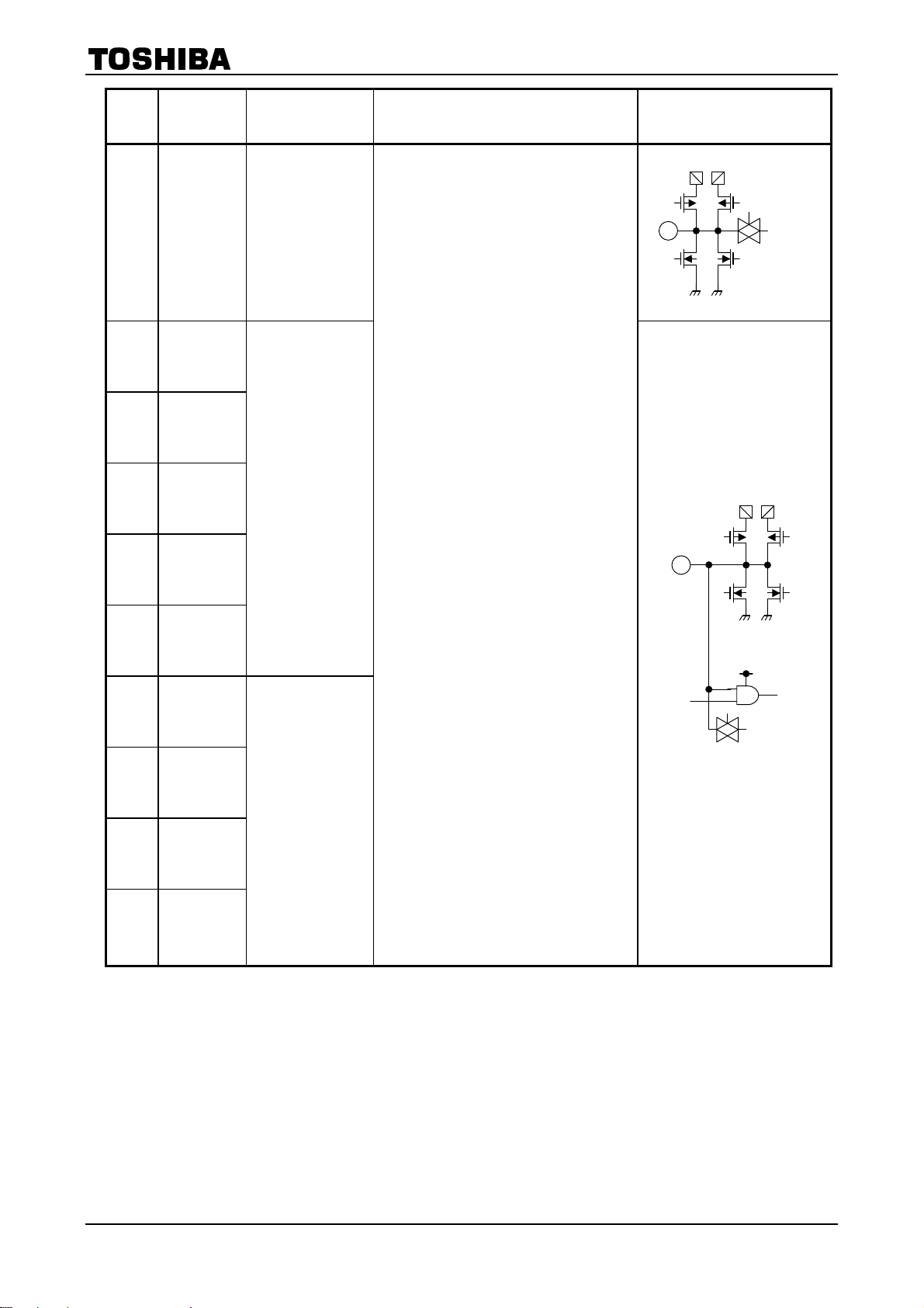
Note: Symbols used for the pins above indicate the following pin functions.
*
: CD processor-dedicated pin
M
: Power supply pin
3
: CD processor tri-state output pin
A
: CD processor analog input/output pin
R
: Reference input pin
M
: Controller-dedicated pin
Note: When the CD is off, the power supply pins for the controller (MV
supply pins (indicated by asterisk *) are off.
) and the power pins supply for the CD oscillator (XV
DD
DD
DV
(
)
X
(
)
()(
)
(
)
(
)
DV
DV
DD
1 bit DAC
RL
LO
SL
V
DD
V
SS
P2-0~P2-3
ROM
RAM
Digital equalizer
Automatic adjustment
circuit
CLV
servo
Sub code decoder
Digital out Audio out
CD Reset
Synchronous
guarantee EFM
decode
16 k SRAM
Correction circuit
IN1
MXO
MXI
P1-3
P1-0
INTR
P4-3 (SCK/SCL)
P4-2
SI0/SI1/SDA
P4-1 (SI2)
P4-0 (ADin4/BUZR)
SBSY
X’tal OSC
Port1
Timer
Interrupt
Cont.
Serial
Interface
Port4
BUZR
MPX
CPU clock
Micon interface
SBSY
CLCK, DATA, SFSY,
Reset
OT19-22
LRCK, BCK, MBOV, IP F
Data Reg (16 bit)
G-Reg. R/W Buf.
ROM
(16 ´ 8192 Step)
RAM
ALU
(4 ´ 512 word)
Program
Counter
Instruction
Decoder
P3-3 (ADin3)
P3-2 (ADin2)
P3-1 (ADin1)
P3-0
AD
Conv.
Port3
Stack Reg.
(8Level)
Bias
COM1 (OT1)
COM2 (OT2)
ZDET, CLCK, DATA, SFSY, LRCK, BCK, MBOV , IPF
LCD Driver/Output Port Port8
S2 (OT6)
S1 (OT5)
COM3 (OT3)
COM4 (OT4)
S10 (OT14/ZDET)
S11 (OT15/CLCK)
S13 (OT17/SFSY)
S12 (OT16/DATA)
S14 (OT18/LRCK)
Reset
Power on Reset
P8-0 (S15/BCK)
P8-1 (S16/AOUT)
Pin Function
TC94A23F
Pin
Number
97 COM1/OT1
98 COM2/OT2
99 COM3/OT3
100 COM4/OT4
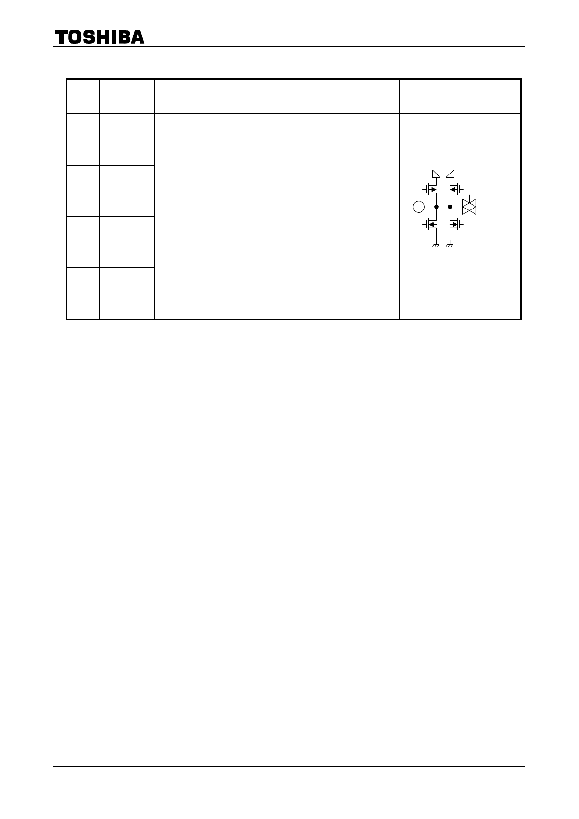
Symbol Pin Name Function and Operation Remarks
LCD common output
/output port
Common signal output pins for the LCD panel.
Those pins configure matrix with S1 to S18
and display up to 72 segments.
The LCD can be driven by the 1/2 or 1/3 bias
method. When the 1/2 bias method is set,
three levels, MV
output at 2-ms intervals at a 62.5 Hz cycle.
When the 1/3 bias method is set, four levels,
MV
, 1/3MVDD, 2/3MVDD, and GND, are
DD
output at 1-ms intervals at a 125 Hz cycle
(when either the 4.5 MHz or 75 kHz crystal
oscillator is used).
After system reset or clock stop execution is
released, the non-selected waveform (bias
voltage) is output. The DISP OFF bit is set to
0 and the common signal is output.
These pins can be switched to an output port
(Note 1) or LED driver pins by program. They
are usually used for digit output to drive the
LEDs.
, 1/2MVDD, and GND, are
DD
MV
DD
MV
DD
Bias
voltage
5
2002-02-06
TC94A23F
Pin
Number
1~9
10
11
12
13
14
15
16
17
18
Symbol Pin Name Function and Operation Remarks
S1/OT4
~
S9/OT13
S10/OT14
/ZDET
S11/OT15
/CLCK
S12/OT16
/DATA
S13/OT17
/SFSY
S14/OT18
/LRCK
P8-0/S15
/BCK
P8-1/S16
/AOUT
P8-2/S17
/MBOV
P8-3/S18
/IPF
LCD segment output
/output port
LCD segment output
/output port
/CD signal
I/O port
/LCD segment output
/CD signal
Segment signal output pins for the LCD panel.
Those pins configure a matrix with COM1 to
COM4 and display up to 72 segments.
When the 1/2 bias method is set, two levels,
and GND, are output. When the 1/3
MV
DD
bias method is set four levels, MV
1/3MV
The S1 to S14 pins can be switched to an
output port (Note 1) by program. Port 8 and
S15 to S18 pins can be switched pin by pin to
an I/O port and segment output pins. When
the pins are set to an I/O port, output is
N-channel open drain.
The S10 to S14 and P8-0 to P8-3 pins can be
switched to CD signal input/output pins by
program. Setting the CD10 bit to 1 switches
the pins to the LRCK, BCK, and AOUT pins as
the CD pins in batches. The other pins can be
individually switched according to the
S14/S15/S16 segment data.
CLCK: Inputs/outputs sub code P to W data
DATA: Outputs sub code P to W data.
SFSY: Outputs frame sync signal for
LRCK: Outputs channel clock (44.1 kHz).
BCK: Outputs bit clock (1.4112 MHz).
AOUT: Outputs audio data.
MBOV: Outputs buffer-memory-overflow
IPF: Outputs interpolation pointing flag. If
ZDET: Outputs 1-bit DAC zero detection flag.
segment output for the LED driver. The output
(Note 1) After a system reset, pins also used
, 2/3MVDD, and GND, are output.
DD
reading clock.
playback.
When L channel, outputs Low. When
R channel, outputs High. The polarity
can be inverted by command.
signal. When buffer memory
overflows, outputs H.
AOUT output is C2 error
detection/correction, outputs High to
indicate correction is impossible.
Pins set as an output port are used for
port can increment OT1 to OT18 by
instruction, facilitating access to data in
external RAM and ROM.
as output ports are set to LCD
output; pins also used as I/O ports
are set to I/O port input.
DD
,
MV
DD
Input
instruction
MV
MV
DD
MV
DD
Bias
voltage
DD
Bias
voltage
MV
DD
6
2002-02-06

TC94A23F
r
Pin
Number
21~24 P1-0~P1-3 I/O port 1
25 P3-0 I/O port 3
26~28
29
33 P2-0/EMPHin
34 P2-1/HSO in
35 P2-2/LRCKin
36 P2-3/DATAin
37 IN1/BCKin
Symbol Pin Name Function and Operation Remarks
P3-1/ADin1
~
P3-3/ADin3
P4-0/ADin4
/BUZR
I/O port 3
/A/D analog voltage
input
I/O port 4
/A/D analog voltage
input/buzzer output
I/O port 2
/1-bit DAC input
General-purpose
input port/1-bit DAC
input (VPP input)
4-bit CMOS I/O port.
Input/output can be set for each bit by
program.
The pins can be set to be pulled-up or
pulled-down by program. Thus, they can be
used as key input pins. When the pins are set
to I/O port input, Clock Stop mode and Wait
mode can be released, according to the
change in input to the pins.
5-bit CMOS I/O port.
Input/output can be set for each bit by
program.
P3-1 and P4-0 pins are also used as built-in
6-bit 4-channel A/D converter analog input
pins.
The built-in A/D converter uses successive
approximation. The conversion time is 6
instruction cycles (280 ms) when the 75 kHz
crystal oscillator is used; 198 ms when the 4.5
MHz crystal oscillator is used; 180 ms when
the 16.9344 MHz crystal oscillator is used.
A/D analog input can be set for each pin by
program. The internal power supply (MV
used as the reference voltage.
The P4-0 pin is also used as the buzzer
output pin.
One of four frequencies: 0.75, 1, 1.5, and 3
kHz, can be selected for buzzer output. The
buzzer is output at the selected frequency in
one of four modes: Continuous, single-shot,
10 Hz intermittent, and 10 Hz intermittent at 1
Hz interval.
Settings for the A/D converter and buzzer,
and their control can be performed by
program.
I/O port 2 is a 4-bit CMOS I/O port.
IN1 and IN2 are a 2-bit general-purpose input
port.
Input/output can be set for each bit of I/O port
2 by program.
I/O port 2 and the IN1 pins can be switched to
1-bit DAC input pins by the CD command to
support shock-proofing. In this case, the I/O
port must be set to input.
With the OTP version, the IN2 pin is also used
as the program power supply pin.
DD
) is
R
MV
DD
instruction
MV
MV
IN1
Input
DD
DD
To A/D
converte
MV
MV
MV
MV
DD
DD
DD
DD
89 IN2/ (VPP)
7
2002-02-06

TC94A23F
Pin
Number
30 P4-1/S12
31
32
38 TESTC
88 TESTM
Symbol Pin Name Function and Operation Remarks
P4-2
/SI0/SI1/SDA
P4-3
/SCK/SCL
I/O port 4/serial data
input
/serial data
input/output
/serial clock
input/output
Test mode control
input
3-bit CMOS I/O port.
Input/output can be set for each bit by
program.
These pins are also used as serial interface
(SIO) circuit input/output pins.
SIO is a serial interface supporting 2-line and
3-line methods. Starting from the MSB or LSB,
4 or 8-bit serial data are output to the SO/SDA
pin, or data on the SI1 and SI2 pins are input
to the device at the clock edge on the
SCK/SCL pin. As the seri al operating c l ock
(SCK/SCL), an internal (450/225/150/75 kHz)
or external clock can be selected. Rising or
falling shift can also be selected. The clock
and data output can be N-channel open drain.
These selections facilitate controlling the LSI
and communications between the controllers.
When SIO interrupts are enabled, an interrupt
is generated as soon as execution of the SIO
completes, and the program jumps to address
4. This is effective for performing serial
communications at high speed.
All SIO inputs incorporate a Schmidt circuit.
SIO and its control can be set by program.
Input pins for controlling Tes t mode.
When the pins are at High level, the device is
in Test mode; at Low level, in normal
operation.
Normally, set the pins to Low level or NC
(pull-down resistors are incorporated).
Input instruction + SI0
R
IN2
MV
ON
MV
DD
DD
39~42
HSO
OT19/
OT20/SPCK
OT21/SPDA
OT22/COFS
Output port/CD
control signal output
4-bit general-purpose output port.
After system reset, the pins are set to a
Low-level output port.
The pins can be switched to CD control output
pins by program. Setting OT19 to OT22 to 0
switches all four pins to CD control output
pins. Setting OT19 to OT22 and CDIO to 1
enables the pins to be switched as follows
according to the segment data contents of the
S15 and S16 pins:
HSO : Outputs playback speed mode.
Normal speed: High
Double speed: Low
SPCK: Outputs clock for reading processor
status signal (176.4 kHz).
APCK: Outputs clock for reading processor
status signal.
SPDA: Outputs processor status signal.
COFS: Outputs frame clock for correction
(7.35 kHz).
MV
DD
8
2002-02-06

TC94A23F
Pin
Number
Symbol Pin Name Function and Operation Remarks
43 DOUT Digital output in.
Sub code block sync output pin.
44 SBSY
When sub code sync is detected, outputs
High at the S1 position.
45 SBOK
Sub code Q data CRCC result output pin.
When the result is OK, outputs High.
Power supply pins for CD digital block.
46, 75 VDD
Normally, 5 V is applied.
When CD is not used (CD off), the power
supply can be set to off except to the
controller, enabling only the controller to
operate. At this time, 1 must be set in the
CDoff bit. If pins from 11 to 18 and 39 to 42
47, 76 VSS
are set as CD control signal input/output pins,
setting the CDoff bit to 1 switches all the pins
to an output port.
48 P2V
2V
REF
pin for PLL block ¾
REF
V
DD
V
DD
MV
SS
P2V
REF
49 PDO
CD processor control
Outputs phase error signal between the EFM
and PLCK signals.
input/output
TMAX detection result output pin. Selected by
command bit TMPS.
Longer than the specified cycle: Outputs
.
P2V
50 TMAX
REF
Shorter than the specified cycle: Outputs Low
SS
).
level (V
Within the specified cycle: at high impedance
51 LPFN Inverted input pin for low-pass filter amp.
52 LPFO Output pin for low-pass filter amp.
53 PV
V
REF
pin for PLL block
REF
54 VCOF VCO filter pin
55 AVSS
Ground pin for analog block ¾
LPFN
LPFO
PV
REF
VCOF
PV
PV
REF
REF
P2V
REF
AV
DD
VCO
9
2002-02-06

TC94A23F
Pin
Number
56 SLCO DAC output pin for generating data slice level
57 RFI RF signal input pin
58 AVDD Power supply pin for analog block ¾
59 RFCT RFRP signal center level input pin
60 RFZI RFRP zero-cross signal input pin
61 RFRP RF ripple signal input pin
62 FEI Focus error signal input pi n
Symbol Pin Name Function and Operation Remarks
RFI
SLCO
RFZI
RFCT
RFRP
CD processor control
input/output
FEI
Z
in1
V
REF
AV
DD
DAC
AV
DD
1 kW typ. 32 kW typ.
AV
DD
63 SBAD Sub beam addition signal input pin
64 TEI
65 TEZI Tracking error/ zero-cross signal input pin
66 FOO Focus equalizer output pin
67 TRO Tracking equalizer output pin
68 V
REF
Tracking error input pin.
The pin is read at tracking servo on.
Analog reference voltage power supply pin ¾
SBAD
TEZI
TEI
Z
in2
V
REF
1 kW typ. 32 kW typ.
R
out3
AVDD
AV
2V
DD
REF
AV
~
SS
10
2002-02-06

TC94A23F
Pin
Number
69 RFGC
70 TEBC
71 FMO
72 DMO
73 2V
74 SEL
Symbol Pin Name Function and Operation Remarks
REF
CD processor control
input/output
Control signal output pin for adjusting RF
amplitude.
Outputs three-level PWM signal
(PWM carrier = 88.2 kHz).
Tracking balance control signal output pin.
Outputs three-level PWM signal
(PWM carrier = 88.2 kHz).
Focus equalizer output pin.
Outputs three-level PWM signal
(PWM carrier = 88.2 kHz).
Disc equalizer output pin.
Outputs three-level PWM signal
(PWM carrier = 88.2 kHz for DSP block).
Analog reference voltage power supply pin
(2 ´ V
APC circuit on/off signal output pin.
At laser on, high impedance at UHS = High; H
level output at UHS = High.
REF
)
P2V
REF
R
out3
V
REF
¾
V
DD
77 XVSS
80 XVDD
78 XI
CD processor crystal
79 XO
oscillator pins
Power supply pins for CD crystal oscillator.
To control the CD processor power supply
and the controller power supply individually,
connect the MV
power supply lines used by the V
pins.
CD crystal oscillator input/output pins.
Connect a 16.9344 MHz crystal oscillator. The
clock is used as the CD system clock and
After system reset, this clock is supplied as
the controller system clock and starts the
CPU.
The crystal oscillator can be halted by
program. If the 4.5 MHz or 75 kHz oscillator is
selected as the controller system clock, the
oscillator is halted by program when the CD
processor is off.
During execution of the CKSTP instruction,
(Note) When switching the controller
system clock from the controller
oscillator to the CD crystal oscillator,
make sure that the CD crystal
oscillator is in stable state.
and MVSS pins to the
DD
controller system clock.
oscillation halts.
DD
and VSS
¾
R
out1
XO
XI
R
fXT1
XV
DD
XV
SS
11
2002-02-06

TC94A23F
Pin
Number
81 DVSR R-channel D/A converter block ground pin
82 RO R-channel data forward rotation output pin
83 DVRR R-channel reference voltage pin
84 DVDD D/A converter block power supply pin
85 DVRL L-channel reference voltage pin
86 LO L-channel data forward rotation output pin
87 DVSL
90 RST Reset input
91 HOLD
Symbol Pin Name Function and Operation Remarks
CD processor control
input/output
L-channel D/A converter block ground pin
Device system reset signal input pin.
RST is at Low level, reset is
when at 0 V, system
DD
pin (power supply for CD), and
V
DD
enter Backup mode.
Hold mode control
input
While the
applied. When the RST is at High level, the
CD block is in operation, and the controller
program starts from address 0.
Normally, when 2.7 V or higher voltage is
supplied to the MV
reset is applied (power-on reset). Fix the pin
to High level.
Input pin used to request or release hold
state.
Normally, the pin is used for inputting the CD
mode selection signal or battery detection
signal.
Halt states are Clock Stop mode (crystal
oscillator stops oscillation) and Wait mode
(CPU stops). The modes are entered using
the CKSTP and WAIT instructions.
By program, Clock Stop mode can be entered
by detection of Low level on the HOLD pin or
by forced execution. Clock Stop mode can be
released by detection of High level on the
HOLD pin or change in the HOLD pin input.
Executing the CKSTP instruction stops the
clock generator and the CPU, entering
memory backup state. During memory backup
state, current dissipation becomes low (1 mA
or below). The display output and CMOS
output port automatically become Low level.
The N-channel open drain output becomes
off.
Regardless of the HOLD pin input state, Wait
mode is executed and current dissipation
becomes low. Crystal oscillator only on or
CPU operation suspended can be
programmed. When the crystal oscillator only
is on, all displays are at Low level. The other
pins are in Hold state. When CPU operation is
suspended, all states are held except that the
CPU is suspended. Wait mode is released by
a change of the HOLD pin input.
(Note) To use Backup mode, turn off the
DV
/DVRL
RR
RO/LO
DVSL/DVSR
DVDD
DV
DD
V
MV
MV
SS
DD
DD
12
2002-02-06

TC94A23F
Pin
Number
92 INTR
93 MXO
94 MXI
19, 96 MVDD
20, 95 MVSS
Symbol Pin Name Function and Operation Remarks
External interrupt
input
Crystal oscillator pins
for controller
Power supply pins for
controller block
External interrupt input pin.
When interrupts are enabled and a pulse of
1.11 to 3.33 ms or more (13.3 to 40 ms when
the 75 kHz clock is used) is input to this pin,
an interrupt is generated and the program
jumps to address 1. Input logic and
rising/falling edge can be individually selected
for interrupt inputs.
The internal 8-bit timer clock can be selected
for interrupt inputs. Interrupts can be
generated (address 3) by pulse count or the
count value.
Interrupt inputs are Schmidt inputs. The pin
can be used as an input port for inputs such
as remote control signals.
Crystal oscillator pins for the controller.
The oscillator clock is used as a time base for
the clock function as well as the system clock
for the controller. After system reset, the CPU
starts operation using the 16.9344 MHz CD
oscillator (connected to the XI and XO pins).
The oscillator is switched to the controller
oscillator by program. Either a 4.5 MHz
reference oscillator or a 75 kHz oscillator is
connected to the MXO and MXI pins.
The oscillators are switched by a bit used to
select a frequency of 4.5 MHz or 75 kHz. The
oscillators incorporate a feedback resistor.
Switching frequencies automatically switches
the feedback resistor of the crystal oscillator.
75 kHz: Rout2 = 2 KW, RfXT2 = 10 MW typ .
4.5 MHz: Rout2 = 2 KW, RfXT2 = 1 MW typ.
If the operating clock is the CD crystal
oscillator, fix the MXI pin to GND.
During execution of the CKSTP instruction,
oscillation halts.
Selection and control of crystal oscillators are
done by program.
(Note) When the 75 kHz crystal oscillator is
Power supply pins for the controller block.
Normally, V
In backup state (when executing the CKSTP
instruction), current dissipation becomes low
(1 mA or below), dropping the power supply
voltage to 2.0 V.
If 2.7 V or more is applied to these pins when
at 0 V, a system reset is appli ed to the device
and the program starts from address 0
(power-on reset).
The CD processor incorporates a power
supply detector, which detects the power
supply voltage of 2.5 V.
(Note) At power-on reset operation, allow
When not using the power supply detector
function, set the test port pins (TEST#0 to 3)
to all 1s so that the CD processor enters Halt
state. Setting to Halt state reduces current
dissipation by 150 mA (typ.).
used, externally add/connect a
100 kW output resistor.
= 4.5 to 5.5 V.
DD
10 to 100 ms while the device power
supply voltage rises.
MXO
MXI
R
R
fXT2
out2
MV
MV
MV
DD
DD
SS
13
2002-02-06

TC94A23F
>
Maximum Ratings
Characteristic Symbol Rating Unit
Power supply voltage
Input voltage
Power dissipation PD 1400 mW
Operating temperature T
Storage temperature T
(Ta ==== 25°C, VDD ==== MVDD ==== DVDD ==== AVDD, MVDD ==== XVDD)
V
DD
(VDD power
supply pin)
power
(MV
DD
supply pin)
MV
DD
V
-0.3~VDD + 0.3
IN1
V
-0.3~MVDD + 0.3
IN2
-40~85 °C
opr
stg
-0.3~6.0 (MV
-65~150 °C
VDD) V
DD
V
14
2002-02-06

Electrical characterist ics
>
>
(unless otherwise specified, Ta ==== 25°C, VDD ==== MVDD ==== XVDD ==== DVDD ==== AVDD ==== 5 V,
2V
REF
==== P2V
==== 4.2 V, V
REF
REF
==== PV
==== 2.1 V)
REF
TC94A23F
V
(power supply pins for CD processor block: VDD, XVDD, DVDD, AVDD)
DD
Characteristic Symbol
Operating power supply
voltage range
Operating power supply
current
Crystal oscillator standby
current
Crystal oscillator frequency fXT ¾ Ci = Co = 15 pF
V
IDD ¾
XI
X
STBY
Test
Circuit
¾ MVDD = XV
DD
, DVDD, AVDD)
(V
DD
operating at 16.9344 MHz
) 16.9344 MHz crystal oscillator
(XV
¾
DD
¾ (XVDD) 16.9344 MHz crystal oscillator off ¾ 0.01 ¾ mA
DD
connected
MVDD
Operating power supply
voltage range
Memory hold voltage range MVHD ¾
Operating power supply
current
(Note 3)
Memory hold current MIHD ¾
Crystal oscillator frequency
Crystal oscillator start time tst ¾ Crystal oscillator f
(power supply pins for CPU block: MVDD, XVDD) (Note 2)
Characteristic Symbol
MV
MV
MV
MI
MI
MI
MI
MI
MI
f
MXT1
f
MXT2
Test
Circuit
DD1
DD2
DD3
¾
DD1
¾
DD2
¾
DD3
¾
DD4
¾
DD5
¾
DD6
¾ 4.5 MHz crystal oscillator set (Note 1)* ¾ 4.5 ¾ MHz
¾
CPU and CD in operation
= XV
MV
DD
CPU in operation (CD off, 4.5 MHz
¾
/16.9344 MHz crystal oscillator used)
CPU in operation
(CD off, 75 kHz crystal oscillator used)
Crystal oscillator stopped
(executing CKSTP instruction)
CPU in operation
Standby mode
(crystal oscillator
only in operation)
Crystal oscillator stopped
(executing CKSTP instruction)
75 kHz crystal oscillator set,
= 2.7~5.5 V
MV
DD
Test Condition Min Typ. Max Unit
VDD = DVDD = AV
DD
(Note 1)* ¾ 16.9344 ¾ MHz
* 4.5 ~ 5.5 V
DD
¾ 50 60
¾ 2.0 ¾
Test Condition Min Typ. Max Unit
VDD = DVDD = AV
DD
XI = 16.9344 MHz crystal
oscillator connected
MXI = 4.5 MHz crystal
oscillator connected
MXI = 75 kHz crystal
oscillator connected
XI = 16.9344 MHz crystal
oscillator connected
MXI = 4.5 MHz crystal
oscillator connected
MXI = 75 kHz crystal
oscillator connected
= 75 kHz ¾ ¾ 1.0 s
mxt
DD
(Note 1)*
4.5 ~ 5.5
*
4.5 ~ 5.5
*
3.0 ~ 5.5
*
2.0 ~ 5.5
*
¾ 3.0 5.0
¾ 1.4 2.5
¾ 0.3 1.0
¾ 1.5 ¾
¾ 0.25 ¾
¾ 0.1 ¾
¾ 0.1 1.0 mA
¾ 75 ¾ kHz
mA
V
mA
Note 1: Design and set constants according to the crystal oscillator to be connected.
Note 2: The power supply/memory hold current is the value obtained by summing the XVDD and MVDD pin currents.
Note 3: The values are those when the power supply detector function is operating. Setting the function reduces
current dissipation by 150 mA (typ.). (Except in Standby mode)
An asterisk (*) indicates the values are guaranteed when V
= MVDD = XVDD = DVDD = AVDD = 4.5 to 5.5 V, and
DD
Ta = -40 to 85°C.
15
2002-02-06

TC94A23F
LCD common output/output port
Characteristic Symbol
High level
Output current
Low level
1/2 level V
Bias voltage
1/3 level V
2/3 level V
I
OH1
I
OH2
I
OL1
I
OL5
BS2
BS1
BS3
Test
Circuit
¾ VOH = 4.5 V (LCD output) -200 -600 ¾ mA
¾ VOH = 4.5 V (OT output) -15 -30 ¾ mA
¾ VOL = 0.5 V (LCD output) 200 600 ¾ mA
¾ VOL = 0.5 V (OT output) 4.0 10 ¾ mA
¾ No load (LCD output, 1/2 bias method set) 2.3 2.5 2.7
¾ 1.47 1.67 1.87
¾
(COM1/OT1 to COM4/OT4)
Test Condition Min Typ. Max Unit
No load (LCD output, 1/3 bias method set)
3.13 3.33 3.53
Segment output, output ports, I/O ports, and CD function output
(S1/OT4 to S9/OT13, S10/OT14/ZDET to S14/OT18/LRCK, P8-0/S14/BCK to P8-3/S18/IPF, OT19)
Characteristic Symbol
I
High level
Output current
Low level
Input leakage current ILI ¾ VIH = 5.0 V, VIL = 0 V (P8-0~P8-3) ¾ ¾ ±1.0 mA
High level VIH ¾ (P8-0~P8-3, CLCK)
Input voltage
Low level V
Bias voltage
1/3 level V
1/2 level V
OH1
I
OH4
I
OL1
I
OL5
BS1
BS3
I/O port
(P1-0~P4-3)
Test
Circuit
¾ VOH = 4.5 V (LCD output) -200 -600 ¾ mA
= 4.5 V (OT output, CD output,
V
¾
¾ VOL = 0.5 V (LCD output) 200 600 ¾ mA
¾ VOL = 0.5 V (OT output, CD output) 4.0 10 ¾ mA
¾ (P8-0~P8-3, CLCK) 0 ~
IL
¾ 1.47 1.67 1.87
¾
OH
excluding P8-0 to P8-3 pins)
No load (LCD output, 1/3 bias method set)
Test Condition Min Typ. Max Unit
-1.5 -4.0 ¾ mA
MV
DD
´ 0.8
3.13 3.33 3.53
~ MV
MV
´ 0.2
DD
DD
V
V
V
Characteristic Symbol
High level I
Output current
Low level
Input leakage current ILI ¾ VIH = 5.0 V, VIL = 0 V ¾ ¾ ±1.0 mA
High level VIH ¾ ¾
Input voltage
Low level V
Input pull-up/down resistance R
OH3
I
OL3
I
OL5
Test
Circuit
¾ VOH = 4.5 V -0.8 -2.0 ¾
= 0.5 V
V
¾
¾ VOL = 0.5 V (P4-1, P4-2, P4-3 pins) 4.0 10 ¾
¾ ¾ 0 ~
IL
¾ (P1-0 to P1-3 pins) pull-down/up set 25 50 120 kW
IN1
OL
(excluding P4-1, P4-2, P4-3 pins)
Test Condition Min Typ. Max Unit
1.0 3.0 ¾
MV
DD
´ 0.8
~ MV
MV
´ 0.2
DD
DD
HOLD
1-bit DAC data input
Input leakage current ILI ¾ VIH = 5.0 V, VIL = 0 V ¾ ¾ ±1.0 mA
Input voltage
, INTR input port, RST
(EMPHin/
Characteristic Symbol
High level VIH ¾ ¾
Low level V
¾ ¾ 0 ~
IL
input,
RST
in/LRCKin/DATAin/BCKin)
HSO
Test
Circuit
Test Condition Min Typ. Max Unit
Input port
MV
´ 0.8
(IN1/IN2)
DD
~ MV
DD
MV
DD
´ 0.2
mA
V
V
16
2002-02-06

TC94A23F
A/D converter
Characteristic Symbol
Analog input voltage range VAD ¾ ADin1~ADin4 0 ~ MV
Resolution VRES ¾ ¾ ¾ 6 ¾ bit
Total conversion error ¾ ¾ ¾ ¾ ±0.5 ±1.0 LSB
Analog input leakage ILI ¾ VIH = 5.0 V, VIL = 0 V (ADin1~ADin4) ¾ ¾ ±1.0 mA
(ADin1 to ADin4)
Test
Circuit
Test Condition Min Typ. Max Unit
DD
DOUT, SBSY, SBOK, SEL, OT19/
Characteristic Symbol
Output current
High level I
Low level I
OH4
OL4
Test
Circuit
¾ VOH = 4.5 V -1.5 -4.0 ¾
¾ VOL = 0.5 V 1.5 4.0 ¾
, OT20/SPCK, OT21/SPDA, OT22/COFS output
HSO
Test Condition Min Typ. Max Unit
PDO, TMAX, RFGC, TEBC, FMO, DMO, TRO, FOO output
Characteristic Symbol
Output current
Output resistance R
V
output voltage V
REF
High level I
Low level I
Transfer delay time
OH6
OL4
out3
oref
(AOUT, SPDA, DATA, SBSY, SBOK)
Test
Circuit
¾ VOH = 3.8 V, P2V
¾ VOL = 0.5 V, P2V
¾ (RFGC, TEBC, FMO, DMO, TRO, FOO) ¾ 3.3 ¾ kW
¾
(RFGC, TEBC, FMO, DMO, PDD)
= PV
V
REF
Test Condition Min Typ. Max Unit
= 4.2 V (PDO, TMAX) ¾ -2.0 ¾
REF
= 4.2 V (PDO, TMAX) ¾ 6.0 ¾
REF
REF
= 2.1 V
¾ 2.1 ¾ V
V
mA
mA
Characteristic Symbol
Transfer delay
time
High level t
Low level t
pLH
pHL
Test
Circuit
¾ ¾ ¾ 10 ¾
¾ ¾ ¾ 10 ¾
Test Condition Min Typ. Max Unit
1-bit DA converter
Characteristic Symbol
Total harmony distortion THD + N ¾ 1 kHz sine wave, full-scale input ¾ -85 -78
S/N ratio S/N ¾ ¾ 90 98 ¾
Dynamic range DR ¾ 1 kHz sine wave, based on -60dB input 85 90 ¾
Crosstalk CT ¾ 1 k Hz sine wave, f ull-scale input ¾ -90 -85
Analog output level DAC
Test
Circuit
¾ 1 kHz sine wave, full-scale input 1200 1250 1300 mVrms
out
Test Condition Min Typ. Max Unit
ns
dB
17
2002-02-06

TC94A23F
Others
Input pull-down resistance R
XI amp feedback resistance R
XO output resistance R
MXI amp feedback
resistance
MXO output resistance R
Input resistance
Characteristic Symbol
Test
Circuit
¾ (TESTC, TESTM) ¾ 10 ¾ kW
IN2
¾ (XI-XO) 1.0 2.0 4.0 MW
fXT1
¾ (XO) ¾ 0.5 ¾ kW
out1
R
fXT2
out2
Z
Z
in1
in2
¾ When 4.5 MHz crystal set, (MXI-MXO) 0.5 1. 0 2.5
¾ When 75 kHz crystal set, (MXI-MXO) ¾ 10 ¾
¾ (MXO) ¾ 2.0 ¾ kW
¾ Set resistance by (RFI) CD command
¾ (TEZI) ¾ 10 ¾
Test Condition Min Typ. Max Unit
¾ 10 ¾
¾ 5.0 ¾
¾ 2.5 ¾
¾ 1.25 ¾
MW
kW
18
2002-02-06

Package Dimensions
TC94A23F
Weight: 1.6 g (typ.)
19
2002-02-06

TC94A23F
A
RESTRICTIONS ON PRODUCT USE
· TOSHIBA is continually working to improve the quality and reliability of its products. Nevertheless, semiconductor
devices in general can malfunction or fail due to their inherent electrical sensitivity and vulnerability to physical
stress. It is the responsibility of the buyer, when utilizing TOSHIBA products, to comply with the standards of
safety in making a safe design for the entire system, and to avoid situations in which a malfunction or failure of
such TOSHIBA products could cause loss of human life, bodily injury or damage to property.
In developing your designs, please ensure that TOSHIBA products are used within specified operating ranges as
set forth in the most recent TOSHIBA products specifications. Also, please keep in mind the precautions and
conditions set forth in the “Handling Guide for Semiconductor Devices,” or “TOSHIBA Semiconductor Reliability
Handbook” etc..
· The TOSHIBA products listed in this document are intended for usage in general electronics applications
(computer, personal equipment, office equipment, measuring equipment, industrial robotics, domestic appliances,
etc.). These TOSHIBA products are neither intended nor warranted for usage in equipment that requires
extraordinarily high quality and/or reliability or a malfunction or failure of which may cause loss of human life or
bodily injury (“Unintended Usage”). Unintended Usage include atomic energy control instruments, airplane or
spaceship instruments, transportation instruments, traffic signal instruments, combustion control instruments,
medical instruments, all types of safety devices, etc.. Unintended Usage of TOSHIBA products listed in this
document shall be made at the customer’s own risk.
· The products described in this document are subject to the foreign exchange and foreign trade laws.
· The information contained herein is presented only as a guide for the applications of our products. No
responsibility is assumed by TOSHIBA CORPORATION for any infringements of intellectual property or other
rights of the third parties which may result from its use. No license is granted by implication or otherwise under
any intellectual property or other rights of TOSHIBA CORPORATION or others.
000707EB
· The information contained herein is subject to change without notice.
20
2002-02-06
 Loading...