

TOSHIBA TC7WH74FU, TC7WH74FK Technical data
TC7WH74FU/FK
TOSHIBA CMOS Digital Integrated Circuit Silicon Monolithic
TC7WH74FU,TC7WH74FK
D-Type flip flop with preset and clear
Features
• High speed: f
• Low power dissipation: I
• High noise immunity: V
= 170 MHz (typ.) at VCC = 5V
MAX
= 2μA (max) at Ta = 25°C
CC
= V
NIH
= 28% VCC (min)
NIL
• 5.5-V tolerant inputs
• Balanced propagation delays: t
• Wide operating voltage range: V
pLH
CC
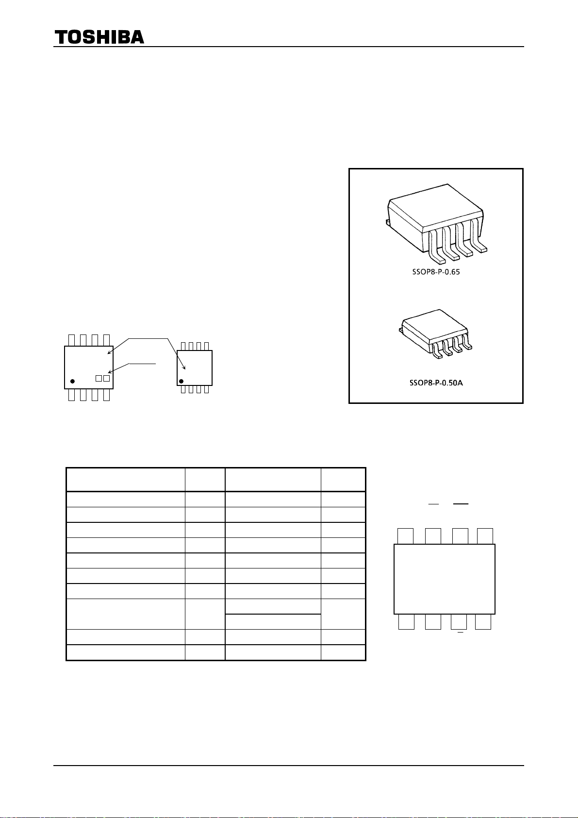
Marking
SM8 US8
H 7 4
Product Name
Lot No.
W H
7 4
Absolute Maximum Ratings
∼
t
−
pHL
= 2 to 5.5V
(Ta = 25°C)
TC7WH74FU
(SM8)
TC7WH74FK
(US8)
Weight
SSOP8-P-0.65: 0.02 g (typ.)
SSOP8-P-0.50A: 0.01 g (typ.)
Characteristics Symbol Rating Unit
Supply voltage V
DC input voltage V
DC output voltage V
Input diode current I
Output diode current I
DC output current I
DC VCC/ground current ICC ±50 mA
Power dissipation PD
Storage temperature T
Lead temperature (10 s) T
CC
IN
OUT
IK
OK
OUT
stg
L
−0.5 to 7.0 V
−0.5 to 7.0 V
−0.5 to VCC + 0.5 V
−20 mA
±20 ( Note 1) mA
±25 mA
300 (SM8)
200 (US8)
−65 to 150 °C
260 °C
mW
Pin Assignment
VCC
PR
8
7
D
CK
2
1
CLR
6
Q
3
(top view)
Q
5
GND
4
Note: Using continuously under heavy loads (e.g. the application of high temperature/current/voltage and the
significant change in temperature, etc.) may cause this product to decrease in the reliability significantly even
if the operating conditions (i.e. operating temperature/current/voltage, etc.) are within the absolute maximum
ratings and the operating ranges.
Please design the appropriate reliability upon reviewing the Toshiba Semiconductor Reliability Handbook
(“Handling Precautions”/“Derating Concept and Methods”) and individual reliability data (i.e. reliability test
report and estimated failure rate, etc).
Note 1: V
< GND、V
OUT
OUT
> VCC
1
2009-09-28
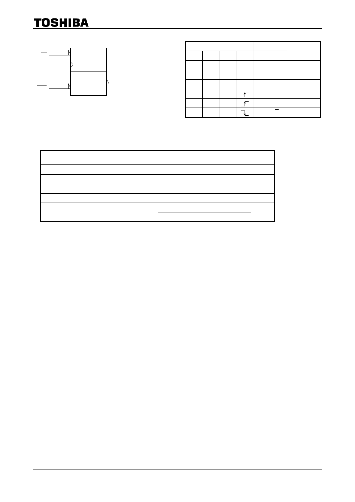
IEC Logic Symbol Truth Table
R
Inputs Outputs
P
CK
CLR
D
S
C
D
R
Q
Q
CLR PR D CK Q Q
L H X X L H Clear
H L X X H L Preset
L L X X H H ⎯
H H L L H ⎯
H H H H L ⎯
H H X Q n Q n No Change
X: Don’t care
Operating Range
Characteristics Symbol Rating Unit
Supply voltage VCC 2.0 to 5.5 V
Input voltage VIN 0 to 5.5
Output voltage V
Operating temperature T
Input rise and fall time dt/dv
0 to V
OUT
opr
0 to 100 (VCC = 3.3 ± 0.3 V)
0 to 20 (V
−40 to 85 °C
CC
= 5.0 ± 0.5 V)
CC
TC7WH74FU/FK
Function
V
V
ns/V
2
2009-09-28
Electrical Characteristics
DC Characteristics
TC7WH74FU/FK
Characteristics Symbol Test Condition
High-level input voltage V
Low-level input voltage V
High-level output voltage VOH
Low-level output voltage VOL
Input leakage current I
Quiescent supply current I
IH
IL
IN
CC
TIMING REQUIREMENTS
Ta = 25°C Ta = −40 to 85°C
V
(V)
CC
2.0 1.5 ⎯ ⎯ 1.5 ⎯
⎯
⎯
IOH = −50 μA
V
= VIH
IN
or V
IL
IOH = −4 mA 3.0 2.58 ⎯ ⎯ 2.48 ⎯
IOH = −8 mA 4.5 3.94 ⎯ ⎯ 3.80 ⎯
IOL = 50 μA
V
= VIH
IN
or V
IL
IOL = 4 mA 3.0 ⎯ ⎯ 0.36 ⎯ 0.44
IOL = 8 mA 4.5 ⎯ ⎯ 0.36 ⎯ 0.44
VIN = 5.5 V or GND 0 to 5.5 ⎯ ⎯ ±0.1 ⎯ ±1.0 μA
VIN = VCC or GND 5.5 ⎯ ⎯ 2.0 ⎯ 20.0 μA
3.0 to
5.5
2.0 ⎯ ⎯ 0.5 ⎯ 0.5
3.0 to
5.5
2.0 1.9 2.0 ⎯ 1.9 ⎯
3.0 2.9 3.0 ⎯ 2.9 ⎯
4.5 4.4 4.5
2.0 ⎯ 0.0 0.1 ⎯ 0.1
3.0 ⎯ 0.0 0.1 ⎯ 0.1
4.5
(unless otherwise specified, Input: tr = tf = 3 ns )
Min Typ. Max Min Max
V
CC
× 0.7
⎯ ⎯
⎯ 0.0 0.1 ⎯ 0.1
⎯ ⎯
V
× 0.3
VCC
× 0.7
CC
⎯ 4.4 ⎯
⎯
⎯
V
CC
× 0.3
Unit
V
V
V
V
Characteristics Symbol Test Condition
tW (L)
(CK)
(
CLR , PR )
Minimum setup time ts
Minimum hold time th
(
CLR , PR )
t
(H)
W
(L)
t
W
t
rem
Ta = 25°C Ta = −40 to 85°C
(V) Limit Limit
V
CC
3.3 ± 0.3 6.0 7.0 Minimum pulse width
5.0
± 0.5 5.0 5.0
3.3 ± 0.3 6.0 7.0 Minimum pulse width
5.0
± 0.5 5.0 5.0
3.3 ± 0.3 6.0 7.0
5.0
± 0.5 5.0 5.0
3.3 ± 0.3 0.5 0.5
5.0
± 0.5 0.5 0.5
3.3 ± 0.3 5.0 5.0 Minimum removal time
5.0
± 0.5 3.0 3.0
Unit
ns
3
2009-09-28
 Loading...