

Toshiba TC7WG125FC Technical data
现货库存、技术资料、百科信息、热点资讯,精彩尽在鼎好!
TOSHIBA CMOS Digital Integrated Circuit Silicon Monolithic
TC7WG125FC
Dual Bus Buffer with 3-STATE Output
Features
• High-level output current: IOH/IOL = ±8 mA (min)
at V
• High-speed operation: t
at V
• Operating voltage range: V
• 5.5-V tolerant inputs
• 3.6-V power down protection outputs
= 2.5 ns (typ.)
pd
= 0.9~3.6 V
CC
Absolute Maximum Ratings
Characteristics Symbol Value Unit
= 3 V
CC
= 3.3 V,15pF
CC
(Ta = 25°C)
TC7WG125FC
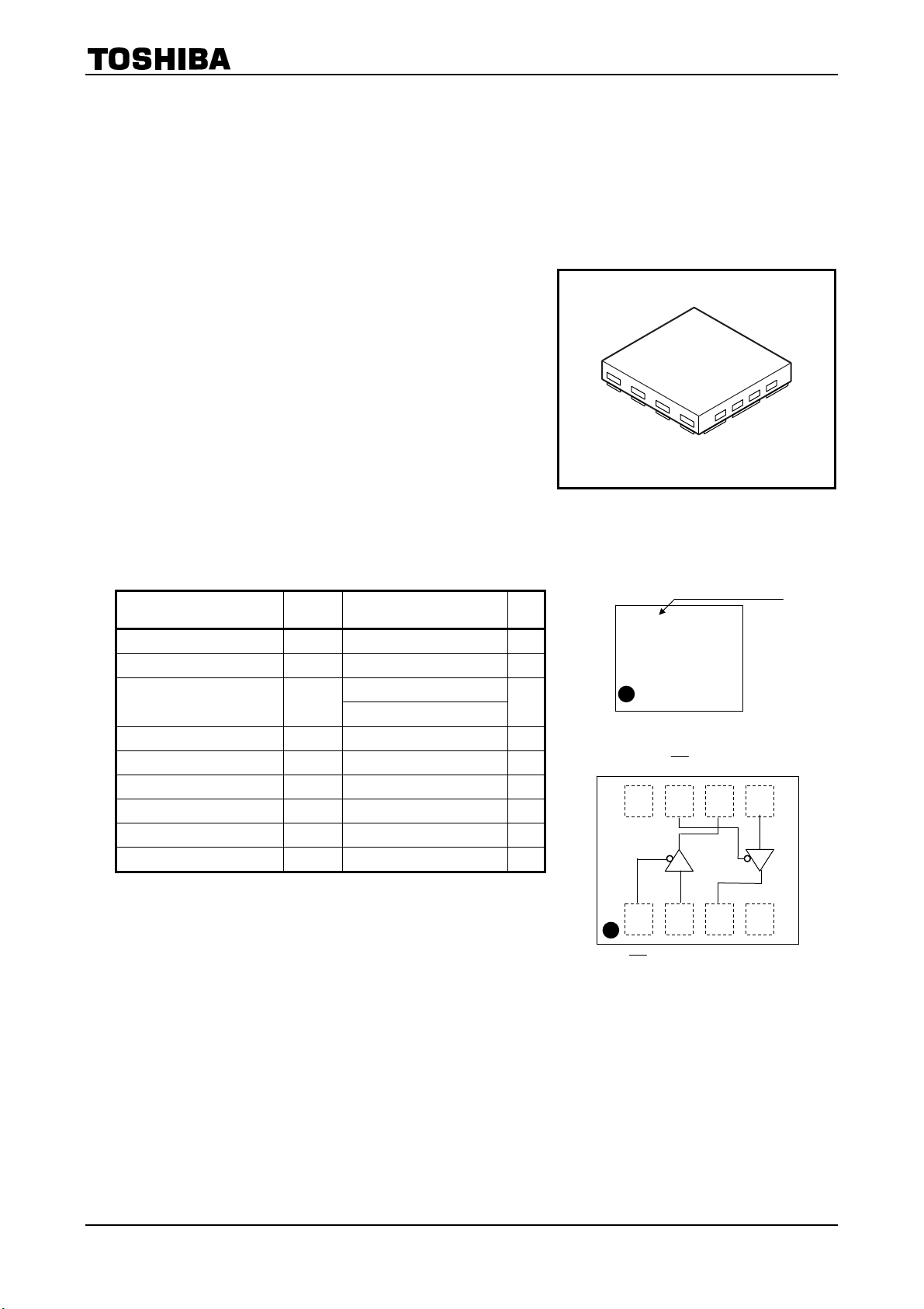
Weight: 0.002 g (typ.)
Marking
TC7WG125FC
CSON8-P-0.4
Product name
Power supply voltage V
DC input voltage V
DC output voltage V
Input diode current I
Output diode current I
DC output current I
DC VCC/GND current I
Power dissipation PD 150 (Note 4) mW
Storage temperature T
Note: Using continuously under heavy loads (e.g. the application of
high temperature/current/voltage and the significant change in
temperature, etc.) may cause this product to decrease in the
reliability significantly even if the operating conditions (i.e.
operating temperature/current/voltage, etc.) are within the
absolute maximum ratings and the operating ranges.
Please design the appropriate reliability upon reviewing the
Toshiba Semiconductor Reliability Handbook (“Handling
Precautions”/Derating Concept and Methods) and individual
reliability data (i.e. reliability test report and estimated failure
rate, etc).
Note 1: V
Note 2: High or Low State.
Note 3: V
Note 4: Mounted on an FR4 board.
= 0 V
CC
I
absolute maximum rating must be observed.
OUT
< GND
OUT
(25.4 mm × 25.4 mm × 1.6 t, Cu Pad: 11.56 mm
CC
IN
−0.5~4.6 (Note 1)
OUT
−0.5~VCC + 0.5 (Note 2)
IK
OK
OUT
CC
−20 (Note 3) mA
−65~150 °C
stg
−0.5~4.6 V
−0.5~7.0 V
−20 mA
±25 mA
±100 mA
2
)
V
G125
Pin Assignment ( top view )
G2 Y1 A2Vcc
8 7 6 5
1 2 3 4
G1 A1 Y2 GND
1
2007-11-01
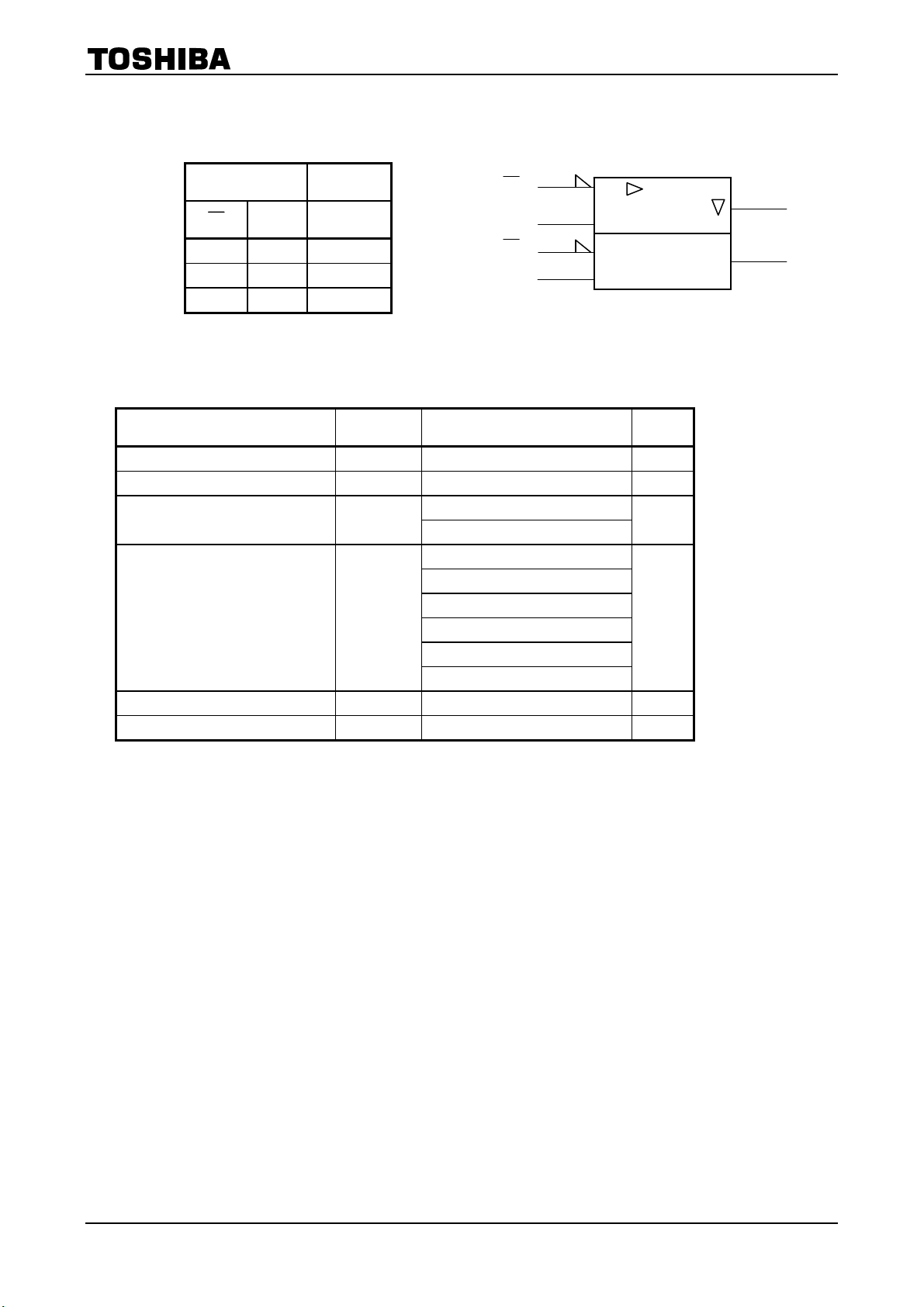
Truth Table
TC7WG125FC
IEC Logic Symbol
Inputs Outputs
G A Y
H X Z
L L L
L H H
G1
A1
G2
A2
EN
X: Don’t Care
Z: High impedance
Operating Ranges
Characteristics Symbol Value Unit
Power supply voltage V
Input voltage VIN 0~5.5 V
Output voltage V
Output Current IOH/IOL
Operating temperature T
Input rise and fall time dt/dV 0~10 (Note 13) ns/V
CC
OUT
opr
0.9~3.6 V
0~3.6 (Note 5)
0~V
±8.0 (Note 7)
±4.0 (Note 8)
±3.0 (Note 9)
±1.7 (Note 10)
±0.3 (Note 11)
±0.02 (Note 12)
−40~85 °C
(Note 6)
CC
V
mA
Y1
Y2
Note 5: VCC = 0 V
Note 6: High or Low state.
Note 7: VCC = 3.0~3.6 V
Note 8: VCC = 2.3~2.7 V
Note 9: VCC = 1.65~1.95 V
Note 10: VCC = 1.4~1.6 V
Note 11: VCC = 1.1~1.3 V
Note 12: VCC = 0.9 V
Note 13: VIN = 0.8~2.0 V, VCC = 3.0 V
2
2007-11-01
Electrical Characteristics
DC Characteristics
TC7WG125FC
Characteristics Symbol Test Condition
High level VIH ⎯
Input voltage
Low level V
IL
High level VOH
Output voltage
Low level V
OL
Input leakage current IIN V
3-state output off-state current IOZ
Power off leakage current I
OFF
Quiescent supply current ICC V
Ta = 25°C Ta = −40~85°C
(V) Min Typ. Max Min Max
V
CC
0.9 V
1.1~1.3
1.4~1.6
1.65~
1.95
V
× 0.7
V
× 0.65
V
× 0.65
⎯ ⎯ VCC ⎯
CC
CC
⎯ ⎯
CC
⎯ ⎯
CC
⎯ ⎯
V
CC
× 0.7
V
CC
× 0.65
V
CC
× 0.65
2.3~2.7 1.7 ⎯ ⎯ 1.7 ⎯
3.0~3.6 2.0 ⎯ ⎯ 2.0 ⎯
0.9 ⎯ ⎯ GND ⎯ GND
V
CC
CC
CC
⎯
⎯
⎯
⎯
1.1~1.3 ⎯ ⎯
1.4~1.6 ⎯ ⎯
1.65~
1.95
⎯ ⎯
× 0.3
V
× 0.35
V
× 0.35
2.3~2.7 ⎯ ⎯ 0.7 ⎯ 0.7
3.0~3.6 ⎯ ⎯ 0.8 ⎯ 0.8
IOH =−0.02 mA 0.9 0.75 ⎯ ⎯ 0.75 ⎯
V
CC
× 0.75
V
CC
× 0.75
V
CC
-0.45
V
IN =VIL
IOH = −0.3 mA 1.1~1.3
IOH = −1.7 mA 1.4~1.6
or
VIH
IOH = −3.0 mA
1.65~
1.95
V
CC
× 0.75
V
CC
× 0.75
V
CC
-0.45
⎯ ⎯
⎯ ⎯
⎯ ⎯
IOH = −4.0 mA 2.3~2.7 2.0 ⎯ ⎯ 2.0 ⎯
I
= −8.0 mA 3.0~3.6 2.48 ⎯ ⎯ 2.48 ⎯
OH
IOL = 0.02 mA 0.9 ⎯ ⎯ 0.1 ⎯ 0.1
V
CC
CC
⎯
⎯
VIN= V
IOL = 0.3 mA 1.1~1.3 ⎯ ⎯
IOL = 1.7 mA 1.4~1.6 ⎯ ⎯
IL
IOL = 3.0 mA
1.65~
1.95
⎯ ⎯ 0.45 ⎯ 0.45
× 0.25
V
× 0.25
IOL = 4.0 mA 2.3~2.7 ⎯ ⎯ 0.4 ⎯ 0.4
IOL = 8.0 mA 3.0~3.6 ⎯ ⎯ 0.4 ⎯ 0.4
= 0~5.5V 0~3.6 ⎯ ⎯ ±0.1 ⎯ ±1.0 μA
IN
V
= VIH or VIL
IN
= 0~3.6V
V
OUT
V
5.5V
IN =
= 3.6V
or V
OUT
= VCC or GND 3.6 ⎯ ⎯ 1.0 ⎯ 10.0 μA
IN
0.9~3.6 ⎯ ⎯ 1.0 ⎯ 10.0 μA
0.0 ⎯ ⎯ 1.0 ⎯ 10.0 μA
⎯
⎯
⎯
V
CC
× 0.3
V
CC
× 0.35
V
CC
× 0.35
⎯
⎯
⎯
V
CC
× 0.25
V
CC
× 0.25
Unit
V
V
3
2007-11-01
 Loading...