

TOSHIBA TC7SA05F, TC7SA05FU Technical data
现货库存、技术资料、百科信息、热点资讯,精彩尽在鼎好!
TOSHIBA CMOS Digital Integrated Circuit Silicon Monolithic
TC7SA05F,TC7SA05FU
Inverter (Open Drain)
Features
• Low voltage operation : VCC = 1.8~3.6 V
• High speed operation : t
: t
: tpz = 8.2 ns (max) (VCC = 1.8 V)
• High Output current : I
: I
: IOH/IOL = ±6 mA (min) (VCC = 1.8 V)
• 3.6-V tolerant input.
• 3.6-V power down protection output.
Absolute Maximum Ratings
= 3.5 ns (max) (VCC = 3.0~3.6 V)
pz
= 4.1 ns (max) (VCC = 2.3~2.7 V)
pz
= ±24 mA (min) (VCC = 3.0 V)
OH/IOL
= ±18 mA (min) (VCC = 2.3 V)
OH/IOL
(Ta = 25°C)
TC7SA05F
TC7SA05FU
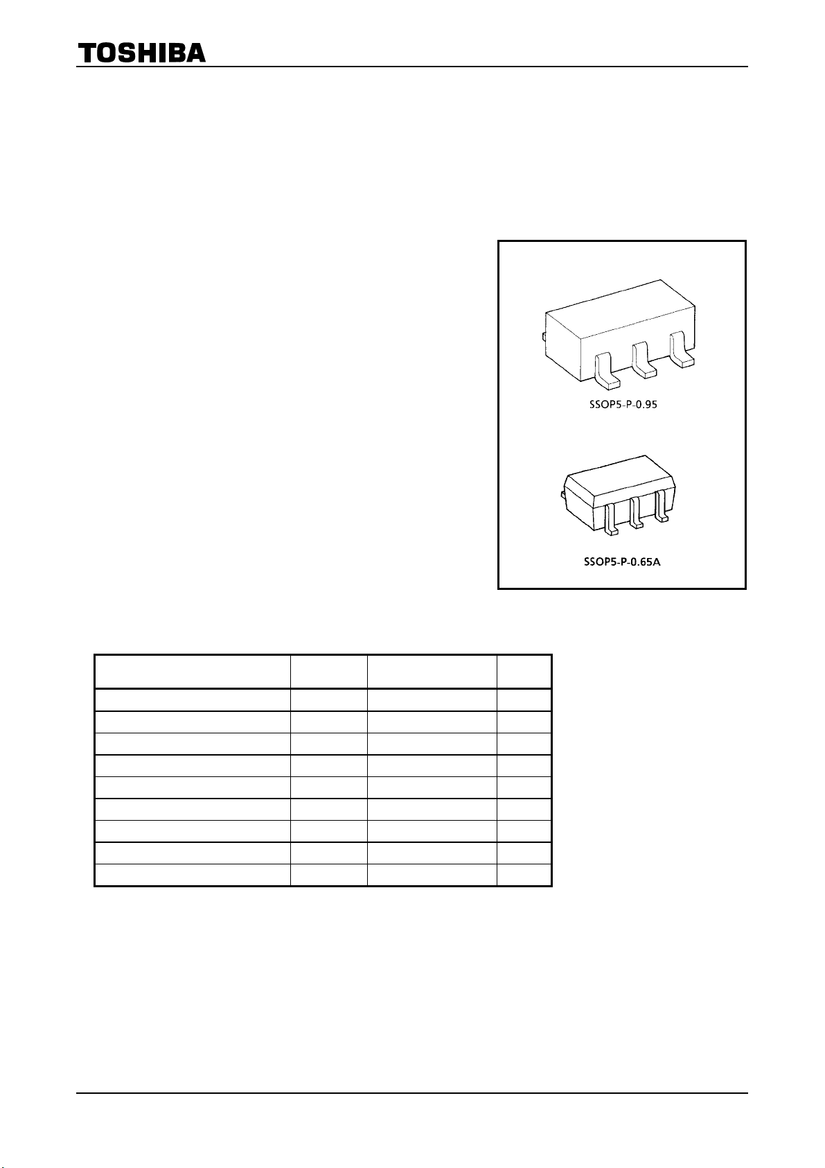
Weight
SSOP5-P-0.95 : 0.016 g (typ.)
SSOP5-P-0.65A : 0.006 g (typ.)
TC7SA05F/FU
Characteristics Symbol Rating Unit
Power supply voltage V
DC input voltage VIN −0.5~4.6 V
DC output voltage V
Input diode current IIK −50 mA
Output diode current IOK −50 (Note 2) mA
DC output current I
Power dissipation PD 200 mW
DC VCC/ground current ICC ±100 mA
Storage temperature range T
Note: Using continuously under heavy loads (e.g. the application of high temperature/current/voltage and the
significant change in temperature, etc.) may cause this product to decrease in the reliability significantly
even if the operating conditions (i.e. operating temperature/current/voltage, etc.) are within the absolute
maximum ratings and the operating ranges.
Please design the appropriate reliability upon reviewing the Toshiba Semiconductor Reliability Handbook
(“Handling Precautions”/“Derating Concept and Methods”) and individual reliability data (i.e. reliability test
report and estimated failure rate, etc).
Note 1: I
Note 2: V
absolute maximum rating must be observed.
OUT
< GND
OUT
CC
−0.5~4.6 (Note 1) V
OUT
±50 mA
OUT
stg
−0.5~4.6 V
−65~150 °C
1
2007-11-01
TC7SA05F/FU
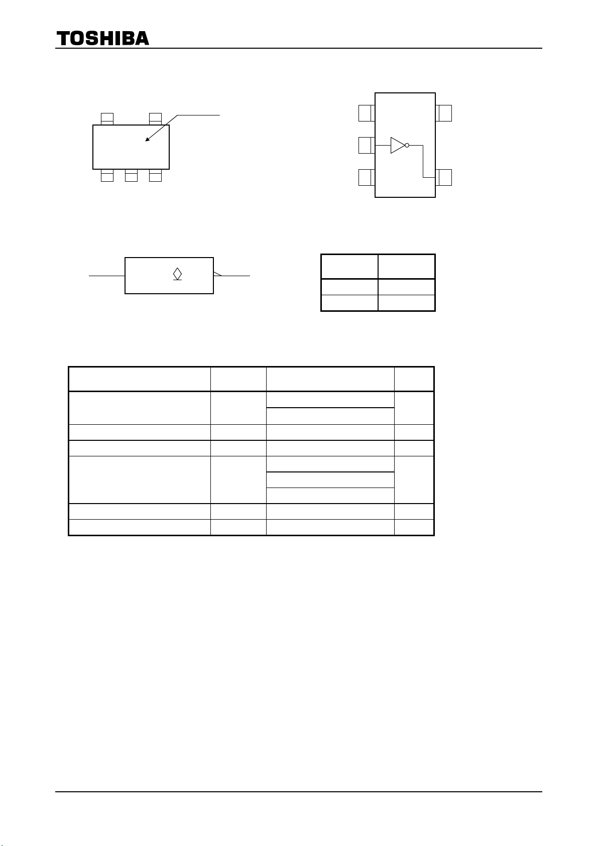
Marking Pin Assignment
(top view)
Type name
V E
NC
IN A
GND
1
2
3
5
4
V
CC
OUT Y
Logic Diagram Truth Table
IN A
1
OUT Y
A Y
L Z
H L
Z: High impedance
Operating Ranges
Characteristics Symbol Rating Unit
Power supply voltage V
Input voltage VIN −0.3~3.6 V
Output voltage V
Output current IOH/IOL
Operating temperature range T
Input rise and fall time dt/dv
CC
OUT
opr
1.8~3.6
1.2~3.6 (Note 3)
0~V
24 (Note 4)
18 (Note 5)
6 (Note 6)
−40~85 °C
0~10 (Note 7) ns/V
CC
V
V
mA
Note 3: Data retention only
Note 4: VCC = 3.0~3.6 V
Note 5: VCC = 2.3~2.7 V
Note 6: VCC = 1.8 V
Note 7: VIN = 0.8~2.0 V, VCC = 3.0 V
2
2007-11-01
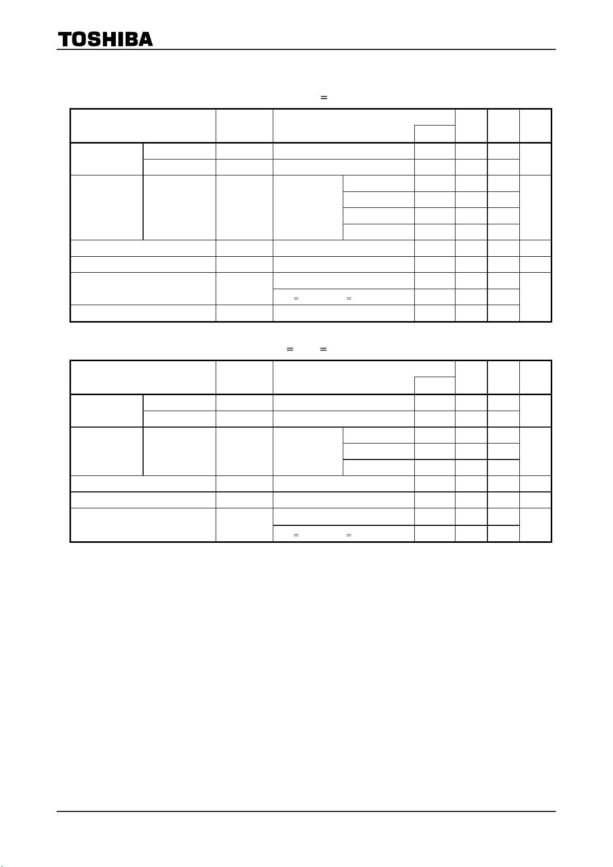
Electrical Characteristics
<
<
<
<
<
<
<
TC7SA05F/FU
DC Characteristics
Characteristics Symbol Test Condition
Input voltage
Output voltage Low level VOL VIN = VIH
Input leakage current IIN VIN = 0~3.6 V 2.7~3.6 ⎯ ±5.0 μA
Power off leakage current I
Quiescent supply current ICC
Increase in ICC per input ΔICC VIH = VCC − 0.6 V 2.7~3.6 ⎯ 750
(Ta = −40~85°C, 2.7 V < V
High level VIH ⎯ 2.7~3.6 2.0 ⎯
Low level V
⎯ 2.7~3.6 ⎯ 0.8
IL
VIN, V
OFF
CC
= 0~3.6 V 0 ⎯ 10.0 μA
OUT
VIN = VCC or GND 2.7~3.6 ⎯ 20.0
(VIN, V
V
CC
OUT
3.6 V)
Min Max Unit
(V)
V
CC
IOL = 100 μA 2.7~3.6 ⎯ 0.2
IOL = 12 mA 2.7 ⎯ 0.4
IOL = 18 mA 3.0 ⎯ 0.4
I
= 24 mA 3.0 ⎯ 0.55
OL
)
3.6 V 2.7~3.6 ⎯ ±20.0
DC Characteristics
Characteristics Symbol Test Condition
Input voltage
Output voltage Low level VOL VIN = VIH
Input leakage current IIN VIN = 0~3.6 V 2.3~2.7 ⎯ ±5.0 μA
Power off leakage current I
Quiescent supply current ICC
(Ta = −40~85°C, 2.3 V
High level VIH ⎯ 2.3~2.7 1.6 ⎯
Low level V
⎯ 2.3~2.7 ⎯ 0.7
IL
VIN, V
OFF
V
CC
= 0~3.6 V 0 ⎯ 10.0 μA
OUT
VIN = VCC or GND 2.3~2.7 ⎯ 20.0
V
(VIN, V
CC
OUT
2.7 V)
Min Max Unit
(V)
V
CC
IOL = 100 μA 2.3~2.7 ⎯ 0.2
IOL = 12 mA 2.3 ⎯ 0.4
= 18 mA 2.3 ⎯ 0.6
I
OL
)
3.6 V 2.3~2.7 ⎯ ±20.0
V
V
μA
V
V
μA
3
2007-11-01
 Loading...