

现货库存、技术资料、百科信息、热点资讯,精彩尽在鼎好!
TOSHIBA CMOS Digital Integrated Circuit Silicon Monolithic
TC7SA04F,TC7SA04FU
Inverter with 3.6 V Tolerant Input and Output
Features
· Low voltage operation : VCC = 1.8~3.6 V
· High speed operation : t
: tpd = 3.7 ns (max) (VCC = 2.3~2.7 V)
: tpd = 7.4 ns (max) (VCC = 1.8 V)
· High Output current : I
: IOH/IOL = ±18 mA (min) (VCC = 2.3 V)
: IOH/IOL = ±6 mA (min) (VCC = 1.8 V)
· Latch-up performance : ±300 mA or more
· ESD performance : Human body model > ±200 V
: Machine model > ±2000 V
· Power down protection is provided on all inputs and outputs.
· TC74VCX04FT equivalent.
Maximum Ratings
= 2.8 ns (max) (VCC = 3.0~3.6 V)
pd
OH/IOL
(Ta = 25°C)
= ±24 mA (min) (VCC = 3.0 V)
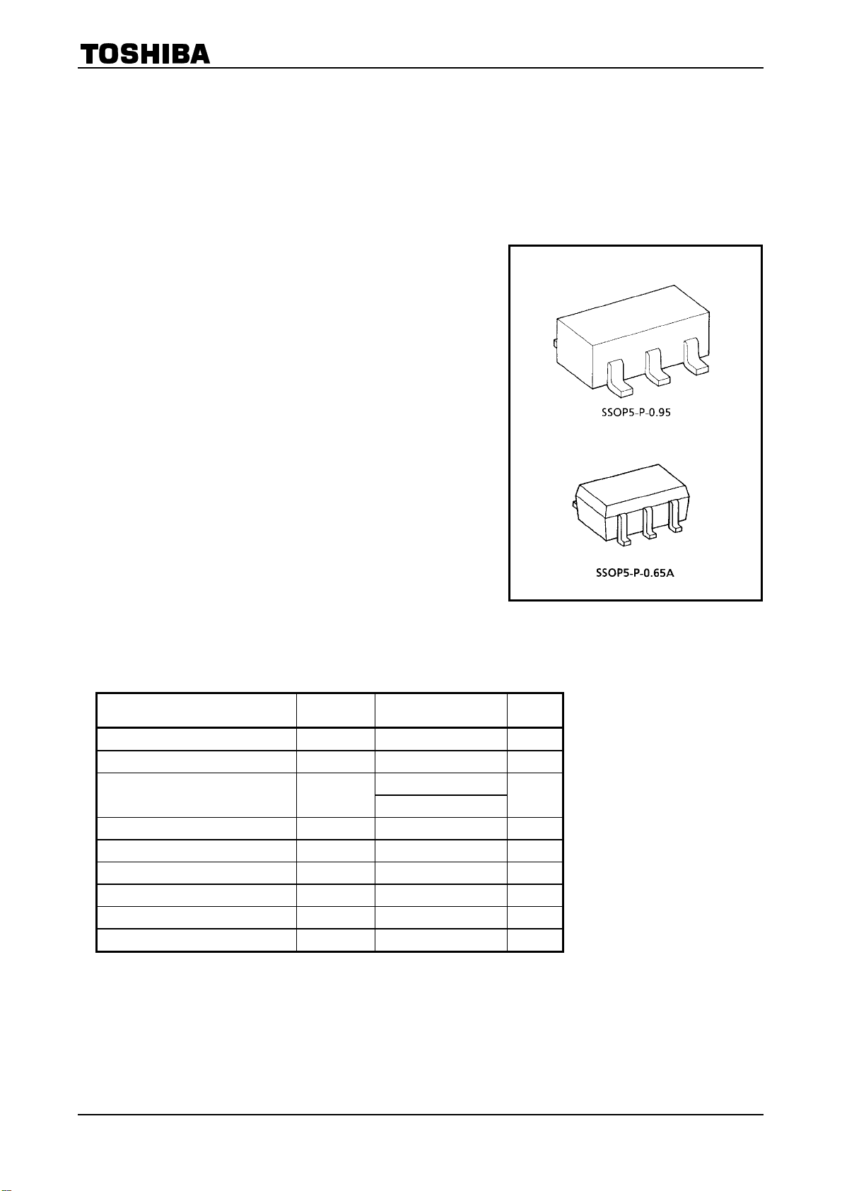
TC7SA04F
TC7SA04FU
Weight
SSOP5-P-0.95 : 0.016 g (typ.)
SSOP5-P-0.65A : 0.006 g (typ.)
TC7SA04F/FU
Characteristics Symbol Rating Unit
Power supply voltage V
DC input voltage VIN −0.5~4.6 V
DC output voltage V
Input diode current IIK −50 mA
Output diode current IOK ±50 (Note 3) mA
DC output current I
Power dissipation PD 200 mW
DC VCC/ground current ICC ±100 mA
Storage temperature range T
Note 1: VCC = 0 V
Note 2: High or low state. I
Note 3: V
OUT
< GND, V
absolute maximum rating be observed.
OUT
> VCC
OUT
CC
OUT
±50 mA
OUT
stg
−0.5~4.6 V
−0.5~4.6 (Note 1)
−0.5~V
+ 0.5 (Note 2)
CC
−65~150 °C
V
1
2002-12-13
TC7SA04F/FU
A
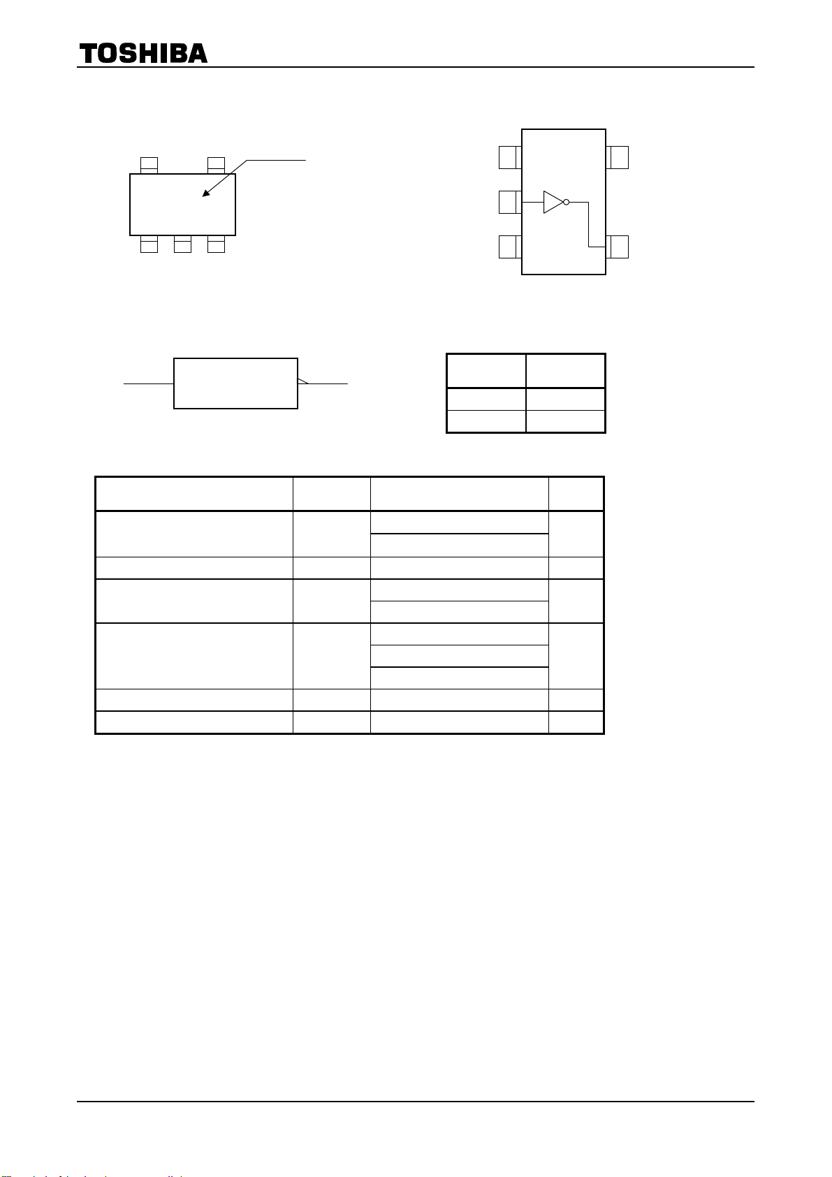
Marking Pin Assignment
(top view)
Type name
V 5
NC
IN A
GND
1
2
3
5
4
V
CC
OUT Y
Logic Diagram Truth Table
IN
1
OUT Y
A Y
L H
H L
Recommended Operating Range
Characteristics Symbol Rating Unit
Power supply voltage V
Input voltage VIN -0.3~3.6 V
Output voltage V
Output current IOH/IOL
Operating temperature range T
Input rise and fall time dt/dv
CC
OUT
opr
1.8~3.6
1.2~3.6 (Note 4)
0~3.6 (Note 5)
0~V
±24 (Note 7)
±18 (Note 8)
±6 (Note 9)
-40~85 °C
0~10 (Note 10) ns/V
CC
(Note 6)
V
V
mA
Note 4: Data retention only
Note 5: VCC = 0 V
Note 6: High or low state
Note 7: VCC = 3.0~3.6 V
Note 8: VCC = 2.3~2.7 V
Note 9: VCC = 1.8 V
Note 10: VIN = 0.8~2.0 V, VCC = 3.0 V
2
2002-12-13

Electrical Characteristics
<
<
DC Characteristics
(Ta ==== ----40~85°C, 2.7 V < V
CC
<<<<
3.6 V)
=
=
TC7SA04F/FU
Characteristics Symbol Test Condition
Input voltage
Output voltage
Input leakage current IIN VIN = 0~3.6 V 2.7~3.6 ¾ ±5.0 mA
Power off leakage current I
Quiescent supply current ICC
Increase in ICC per input DICC VIH = VCC - 0.6 V 2.7~3.6 ¾ 750
High level VIH ¾ 2.7~3.6 2.0 ¾
Low level V
High level VOH VIN = VIL
Low level V
¾ 2.7~3.6 ¾ 0.8
IL
IOH = -100 mA 2.7~3.6
IOH = -12 mA 2.7 2.2 ¾
IOH = -18 mA 3.0 2.4 ¾
I
= -24 mA 3.0 2.2 ¾
OH
IOL = 100 mA 2.7~3.6 ¾ 0.2
VIN = VIH
OL
VIN, V
OFF
= 0~3.6 V 0 ¾ 10.0 mA
OUT
VIN = VCC or GND 2.7~3.6 ¾ 20.0
(VIN, V
V
CC
IOL = 12 mA 2.7 ¾ 0.4
IOL = 18 mA 3.0 ¾ 0.4
= 24 mA 3.0 ¾ 0.55
I
OL
)<3.6 V 2.7~3.6 ¾ ±20.0
OUT
V
CC
Min Max Unit
(V)
V
CC
- 0.2
¾
DC Characteristics
(Ta ==== ----40~85°C, 2.3 V
=
<<<<
=
<<<<
V
CC
2.7 V)
=
=
V
V
mA
Characteristics Symbol Test Condition
Input voltage
Output voltage
Input leakage current IIN VIN = 0~3.6 V 2.3~2.7 ¾ ±5.0 mA
Power off leakage current I
Quiescent supply current ICC
High level VIH ¾ 2.3~2.7 1.6 ¾
Low level V
High level VOH VIN = VIL
Low level V
¾ 2.3~2.7 ¾ 0.7
IL
IOH = -100 mA 2.3~2.7
IOH = -6 mA 2.3 2.0 ¾
IOH = -12 mA 2.3 1.8 ¾
I
= -18 mA 2.3 1.7 ¾
OH
IOL = 100 mA 2.3~2.7 ¾ 0.2
VIN = VIH
OL
VIN, V
OFF
= 0~3.6 V 0 ¾ 10.0 mA
OUT
VIN = VCC or GND 2.3~2.7 ¾ 20.0
(VIN, V
V
CC
IOL = 12 mA 2.3 ¾ 0.4
I
= 18 mA 2.3 ¾ 0.6
OL
)<3.6 V 2.3~2.7 ¾ ±20.0
OUT
V
CC
Min Max Unit
(V)
V
CC
- 0.2
¾
V
V
mA
3
2002-12-13
DC Characteristics
<
(Ta ==== ----40~85°C, 1.8 V
=
<<<<
=
V
CC
< 2.3 V)
TC7SA04F/FU
Characteristics Symbol Test Condition
High level VIH ¾ 1.8~2.3
Input voltage
Low level V
High level VOH VIN = VIL
Output voltage
Low level V
Input leakage current IIN VIN = 0~3.6 V 1.8 ¾ ±5.0 mA
Power off leakage current I
Quiescent supply current ICC
¾ 1.8~2.3 ¾
IL
IOH = -100 mA 1.8
= -6 mA 1.8 1.4 ¾
I
OH
VIN = VIH
OL
VIN, V
OFF
= 0~3.6 V 0 ¾ 10.0 mA
OUT
VIN = VCC or GND 1.8 ¾ 20.0
(VIN, V
V
CC
IOL = 100 mA 1.8 ¾ 0.2
I
= 6 mA 1.8 ¾ 0.3
OL
)<3.6 V 1.8 ¾ ±20.0
OUT
V
CC
Min Max Unit
(V)
0.7 ´
V
CC
V
CC
- 0.2
¾
0.2 ´
V
CC
¾
AC Characteristics
Characteristics Symbol Test Condition
Propagation delay time
(Ta ==== ----40~85°C, input: tr ==== tf ==== 2.0 ns, CL ==== 30 pF, RL ==== 500 WWWW)
V
(V)
CC
t
pLH
t
pHL
Figure 1, Figure 2
1.8 1.0 7.4
2.5 ± 0.2 0.8 3.7
3.3 ± 0.3 0.6 2.8
Min Max Unit
V
V
mA
ns
For CL = 50 pF, add approximately 300 ps to the AC maximum specification.
4
2002-12-13

TC7SA04F/FU
Dynamic Switching Characteristics
Characteristics Symbol Test Condition
Quiet output maximum dynamic VOL V
Quiet output minimum dynamic VOL V
Quiet output minimum dynamic VOH V
OLP
OLV
OLP
(Ta ==== 25°C, input: tr ==== tf ==== 2.0 ns, CL ==== 30 pF)
V
CC
VIN = 1.8 V, VIL = 0 V (Note 11) 1.8 0.25
VIN = 2.5 V, VIL = 0 V (Note 11) 2.5 0.6
= 3.3 V, VIL = 0 V (Note 11) 3.3 0.8
V
IN
VIN = 1.8 V, VIL = 0 V (Note 11) 1.8 -0.25
VIN = 2.5 V, VIL = 0 V (Note 11) 2.5 -0.6
VIN = 3.3 V, VIL = 0 V (Note 11) 3.3 -0.8
VIN = 1.8 V, VIL = 0 V (Note 11) 1.8 1.5
VIN = 2.5 V, VIL = 0 V (Note 11) 2.5 1.9
V
= 3.3 V, VIL = 0 V (Note 11) 3.3 2.2
IN
(V)
Typ. Unit
ns
ns
ns
Note 11: Parameter guaranteed by design.
Capacitive Characteristics
Characteristics Symbol Test Condition
Input capacitance CIN ¾ 1.8, 2.5, 3.3 5 pF
Power dissipation capacitance CPD fIN = 10 MHz (Note 12) 1.8, 2.5, 3.3 18 pF
(Ta ==== 25°C)
V
(V)
CC
Typ. Unit
Note 12: CPD is defined as the value of the internal equivalent capacitance which is calculated from the operating
current consumption without load.
Average operating current can be obtained by the equation.
I
CC (opr)
= CPD・VCC・fIN + I
CC
5
2002-12-13

AC Test Circuit
r
Output
TC7SA04F/FU
Measure
AC Wareform
Input
Output
L
C
L
R
C
= 30 pF
L
R
= 500 W
L
Figure 1
2.0 ns 2.0 nst
t
pLH
t
f
90%
VM
10%
V
M
t
pHL
Symbol
VIH 2.7 V VCC V
VM 1.5 V VCC/2 VCC/2
3.3 ± 0.3 V 2.5 ± 0.2 V 1.8 V
VIH
V
OH
V
OL
VCC
CC
Figure 2 t
pLH
,
t
pHL
6
2002-12-13

Package Dimensions
TC7SA04F/FU
Weight: 0.016 g (typ.)
7
2002-12-13

Package Dimensions
TC7SA04F/FU
Weight: 0.006 g (typ.)
8
2002-12-13

TC7SA04F/FU
A
RESTRICTIONS ON PRODUCT USE
· TOSHIBA is continually working to improve the quality and reliability of its products. Nevertheless, semiconductor
devices in general can malfunction or fail due to their inherent electrical sensitivity and vulnerability to physical
stress. It is the responsibility of the buyer, when utilizing TOSHIBA products, to comply with the standards of
safety in making a safe design for the entire system, and to avoid situations in which a malfunction or failure of
such TOSHIBA products could cause loss of human life, bodily injury or damage to property.
In developing your designs, please ensure that TOSHIBA products are used within specified operating ranges as
set forth in the most recent TOSHIBA products specifications. Also, please keep in mind the precautions and
conditions set forth in the “Handling Guide for Semiconductor Devices,” or “TOSHIBA Semiconductor Reliability
Handbook” etc..
· The TOSHIBA products listed in this document are intended for usage in general electronics applications
(computer, personal equipment, office equipment, measuring equipment, industrial robotics, domestic appliances,
etc.). These TOSHIBA products are neither intended nor warranted for usage in equipment that requires
extraordinarily high quality and/or reliability or a malfunction or failure of which may cause loss of human life or
bodily injury (“Unintended Usage”). Unintended Usage include atomic energy control instruments, airplane or
spaceship instruments, transportation instruments, traffic signal instruments, combustion control instruments,
medical instruments, all types of safety devices, etc.. Unintended Usage of TOSHIBA products listed in this
document shall be made at the customer’s own risk.
· The products described in this document are subject to the foreign exchange and foreign trade laws.
· The information contained herein is presented only as a guide for the applications of our products. No
responsibility is assumed by TOSHIBA CORPORATION for any infringements of intellectual property or other
rights of the third parties which may result from its use. No license is granted by implication or otherwise under
any intellectual property or other rights of TOSHIBA CORPORATION or others.
000707EB
· The information contained herein is subject to change without notice.
9
2002-12-13
 Loading...