

TOSHIBA TC7MH573FK Technical data
TOSHIBA CMOS Digital Integrated Circuit Silicon Monolithic
TC7MH573FK
Octal D-Type Latch with 3-State Output
The TC7MH573FK is an advanced high speed CMOS octal
latch with 3-state output fabricated with silicon gate C
technology.
It achieves the high speed operation similar to equivalent
bipolar schottky TTL while maintaining the CMOS low power
dissipation.
This 8 bit D-type latch is controlled by a latch enable input
(LE) and an output enable input (OE).
When the OE input is high, the eight outputs are in a high
impedance state.
An input protection circuit ensures that 0 to 7 V can be applied
to the input pins without regard to the supply voltage. This
device can be used to interface 5 V to 3 V systems and two supply
systems such as battery back up. This circuit prevents device
destruction due to mismatched supply and input voltages.
Features
2
MOS
Weight: 0.03 g (typ.)
TC7MH573FK
• High speed: tpd = 4.5 ns (typ.) (VCC = 5 V)
• Low power dissipation: I
• High noise immunity: V
• Power down protection is provided on all inputs.
• Balanced propagation delays: t
• Wide operating voltage range: V
• Low noise: V
• Pin and function compatible with 74ALS573
= 1.0 V (max)
OLP
= 4 μA (max) (Ta = 25°C)
CC
NIH
= V
= 28% VCC (min)
NIL
≈ t
pLH
CC (opr)
pHL
= 2~5.5 V
1
2001-10-23
TC7MH573FK
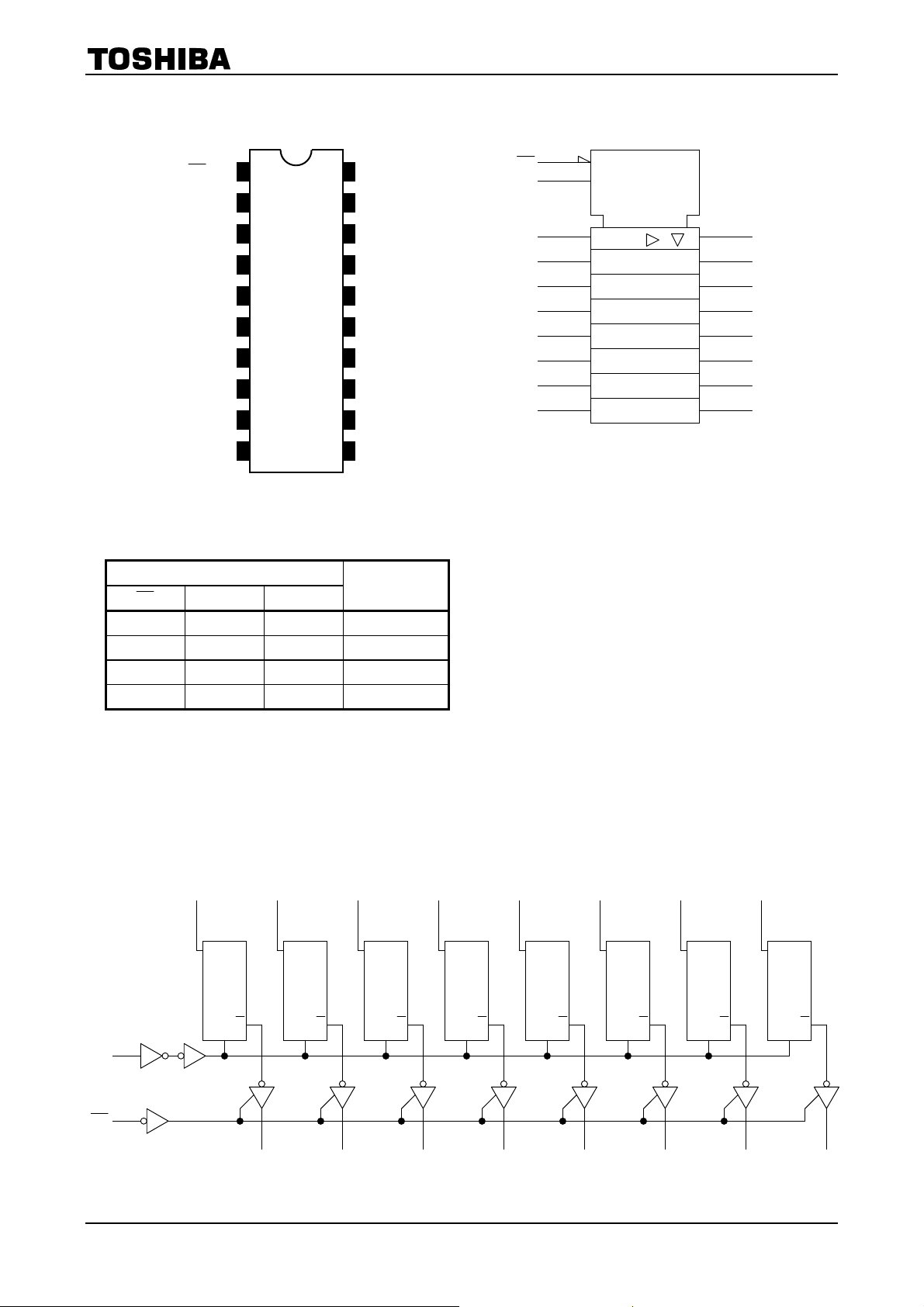
Pin Assignment
OE 1
D0
D1
D2
D3
D4
D5 Q5
D6
D7
10
GND
Truth Table
(top view)
2
3
4
5
6
7
8
9
IEC Logic Symbol
(1)
V
20
CC
Q0
19
Q1
18
Q2
17
Q3
16
Q4
15
14
Q6
13
Q7
12
LE
11
OE
LE
D0
D1
D2
D3
D4
D5
D6
D7
(11)
(2)
(3)
(4)
(5)
(6)
(7)
(8)
(9)
EN
C1
1D
(19)
(18)
(17)
(16)
(15)
(14)
(13)
(12)
Q0
Q1
Q2
Q3
Q4
Q5
Q6
Q7
Inputs
OE LE D
H X X Z
L L X Qn
L H L L
L H H H
Outputs
X: Don’t care
Z: High impedance
: Q outputs are latched at the time when the LE input is taken to a low logic level.
Q
n
System Diagram
D1 D2 D3 D4 D5 D6 D7
3
D
Q
4
D
Q
L
5
D
Q
L
6
D
Q
L
LE
11
D0
2
D
L
7
D
Q
L
8
D
Q
L
9
D
Q
L
Q
L
OE
1
19
Q0
18
Q1
17
Q2
16
Q3
15
Q4
2
14
Q5
13
Q6
2001-10-23
12
Q7
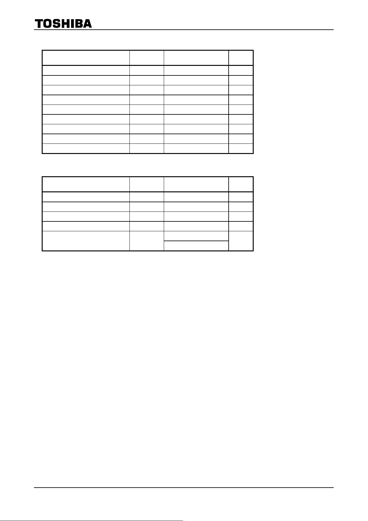
Maximum Ratings
Characteristics Symbol Rating Unit
TC7MH573FK
Supply voltage range V
DC input voltage V
DC output voltage V
Input diode current I
Output diode current I
DC output current I
DC VCC/ground current I
Power dissipation P
Storage temperature T
CC
IN
OUT
IK
OK
OUT
CC
D
stg
Recommended Operating Conditions
Characteristics Symbol Rating Unit
Supply voltage V
Input voltage V
Output voltage V
Operating temperature T
Input rise and fall time dt/dv
CC
IN
OUT
opr
−0.5~V
0~100 (V
0~20 (V
−0.5~7.0 V
−0.5~7.0 V
+ 0.5 V
CC
−20 mA
±20 mA
±25 mA
±75 mA
180 mW
−65~150 °C
2.0~5.5 V
0~5.5 V
0~V
CC
−40~85 °C
= 3.3 ± 0.3 V)
CC
= 5 ± 0.5 V)
CC
V
ns/V
3
2001-10-23
 Loading...