

TOSHIBA TC74VHC153F, TC74VHC153FN, TC74VHC153FT, TC74VHC153FK Technical data
TC74VHC153F/FN/FT/FK
TOSHIBA CMOS Digital Integrated Circuit Silicon Monolithic
TC74VHC153F,TC74VHC153FN,TC74VHC153FT,TC74VHC153FK
Dual 4-Channel Multiplexer
The TC74VHC153 is an advanced high speed CMOS DUAL
4-CHANNEL MULTIPLEXERs fabricated with silicon gate
2
C
MOS technology.
It achieves the high speed operation similar to equivalent
Bipolar Schottky TTL while maintaining the CMOS low power
dissipation.
Each of these data (1C0-1C3, 2C0-2C3) is selected by the two
address inputs A and B.
Separate strobe inputs (
two four-line sections.
The strobe input (
the output is fixed in low level while the strobe input is held
high.
An input protection circuit ensures that 0 to 5.5 V can be
applied to the input pins without regard to the supply voltage.
This device can be used to interface 5 V to 3 V systems and two
supply systems such as battery back up. This circuit prevents
device destruction due to mismatched supply and input voltages.
G1
, G2) are provided for each of the
G
) can be used to inhibit the data output;
Features
• High speed: tpd = 5.0 ns (typ.) at VCC = 5 V
• Low power dissipation: I
• High noise immunity: V
• Power down protection is provided on all inputs.
• Balanced propagation delays: t
• Wide operating voltage range: V
• Pin and function compatible with 74ALS153
= 4 μA (max) at Ta = 25°C
CC
NIH
= V
= 28% VCC (min)
NIL
∼
t
−
pLH
pHL
CC (opr)
= 2 to 5.5 V
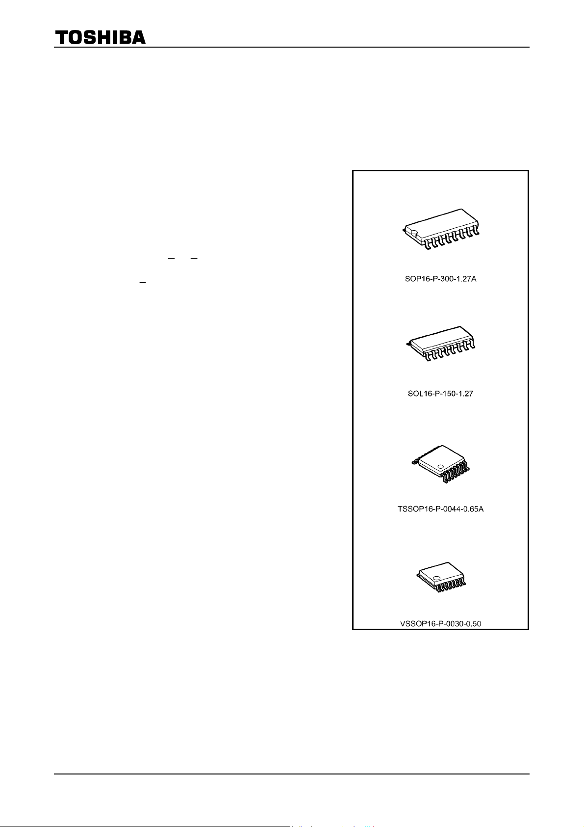
Note: xxxFN (JEDEC SOP) is not available in
Japan.
TC74VHC153F
TC74VHC153FN
TC74VHC153FT
TC74VHC153FK
Weight
SOP16-P-300-1.27A : 0.18 g (typ.)
SOL16-P-150-1.27 : 0.13 g (typ.)
TSSOP16-P-0044-0.65A : 0.06 g (typ.)
VSSOP16-P-0030-0.50 : 0.02 g (typ.)
1
2007-10-01
TC74VHC153F/FN/FT/FK
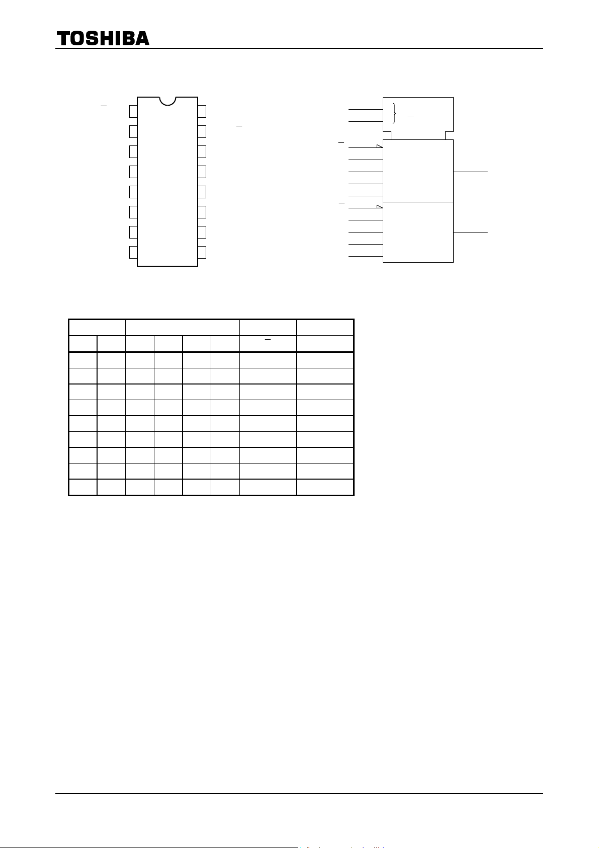
A
Pin Assignment IEC Logic Symbol
(14)
V
G1
1C3
1C2
1C1
1C0
1Y
GND
1
B
2
3
4
5
6
7
8
(top view)
15
14
13
12
11
10
9
CC
G2
2C3
2C2
2C1
2C0
2Y
16
Truth Table
Select Inputs Data Inputs Strobe Output
B A C0 C1 C2 C3 G Y
X X X X X X H L
L L L X X X L L
L L H X X X L H
L H X L X X L L
L H X H X X L H
H L X X L X L L
H L X X H X L H
H H X X X L L L
H H X X X H L H
A
B
G1
1C0
1C1
1C2
1C3
G2
2C0
2C1
2C2
2C3
(2)
(1)
(6)
(5)
(4)
(3)
(15)
(10)
(11)
(12)
(13)
0
1
EN
0
1
2
3
G
0
3
MUX
(7)
(9)
1Y
2Y
X: Don’t care
2
2007-10-01
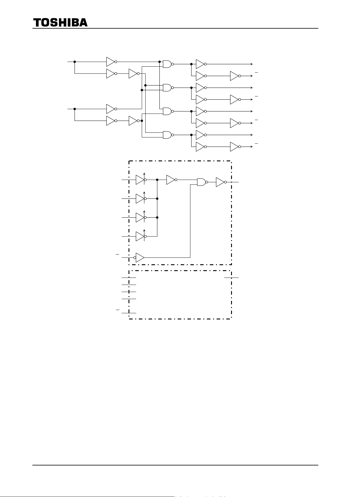
System Diagram
A
14
2
B
TC74VHC153F/FN/FT/FK
S0
0S
S1
1S
S2
2S
S3
3S
1C0
1C1
1C2
1C3
G1
2C0
2C1
2C2
2C3
G2
6
5
4
3
1
10
11
12
13
15
S0
S1
S2
S3
Same as above block
7
1Y
9
2Y
3
2007-10-01
TC74VHC153F/FN/FT/FK
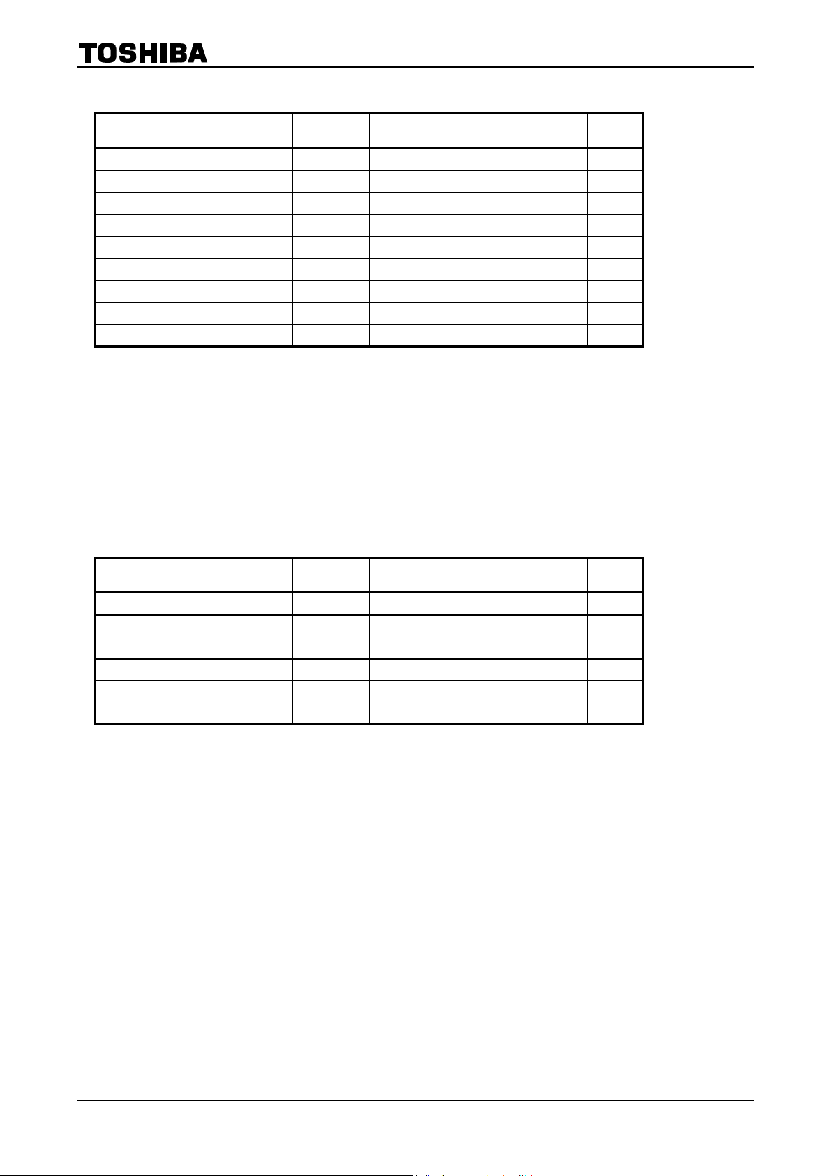
Absolute Maximum Ratings (Note)
Characteristics Symbol Rating Unit
Supply voltage range VCC −0.5 to 7.0 V
DC input voltage VIN −0.5 to 7.0 V
DC output voltage V
Input diode current IIK −20 mA
Output diode current IOK ±20 mA
DC output current I
DC VCC/ground current ICC ±50 mA
Power dissipation PD 180 mW
Storage temperature T
Note: Exceeding any of the absolute maximum ratings, even briefly, lead to deterioration in IC performance or
even destruction.
Using continuously under heavy loads (e.g. the application of high temperature/current/voltage and the
significant change in temperature, etc.) may cause this product to decrease in the reliability significantly
even if the operating conditions (i.e. operating temperature/current/voltage, etc.) are within the absolute
maximum ratings and the operating ranges.
Please design the appropriate reliability upon reviewing the Toshiba Semiconductor Reliability Handbook
(“Handling Precautions”/“Derating Concept and Methods”) and individual reliability data (i.e. reliability test
report and estimated failure rate, etc).
Operating Range
(Note
)
−0.5 to VCC + 0.5 V
OUT
±25 mA
OUT
−65 to 150 °C
stg
Characteristics Symbol Rating Unit
Supply voltage V
Input voltage V
Output voltage V
Operating temperature T
Input rise and fall time dt/dv
CC
IN
OUT
opr
0 to 100 (V
2.0 to 5.5 V
0 to 5.5
0 to V
CC
−40 to 85 °C
= 3.3 ± 0.3 V)
CC
0 to 20 (V
= 5 ± 0.5 V)
CC
Note : The operating range must be maintained to ensure the normal operation of the device.
Unused inputs must be tied to either V
or GND.
CC
V
V
ns/V
4
2007-10-01
 Loading...