TC74VCXR162245FT
TOSHIBA CMOS Digital Integrated Circuit Silicon Monolithic
TC74VCXR162245FT
Low-Voltage 16-Bit Bus Transceiver with 3.6-V Tolerant Inputs and Outputs
The TC74VCXR162245FT is a high-performance CMOS 16-bit
bus transceiver. Designed for use in 1.8-V, 2.5-V or 3.3-V systems,
it achieves high-speed operation while maintaining the CMOS
low power dissipation.
It is also designed with overvoltage tolerant inputs and outputs
up to 3.6 V.
This 16 bit bus transceiver is controlled by direction control
(DIR) inputs and output enable (OE) inputs which are common to
each byte. It can be used as two 8-bit transceivers or one 16-bit
transceiver. The direction of data transmission is determined by
the level of the DIR inputs. The OE inputs can be used to disable
the device so that the busses are effectively isolated.
The 26-Ω series resistor helps reducing output overshoot and undershoot without external resistor.
All inputs are equipped with protection circuits against static discharge.
Features (Note)
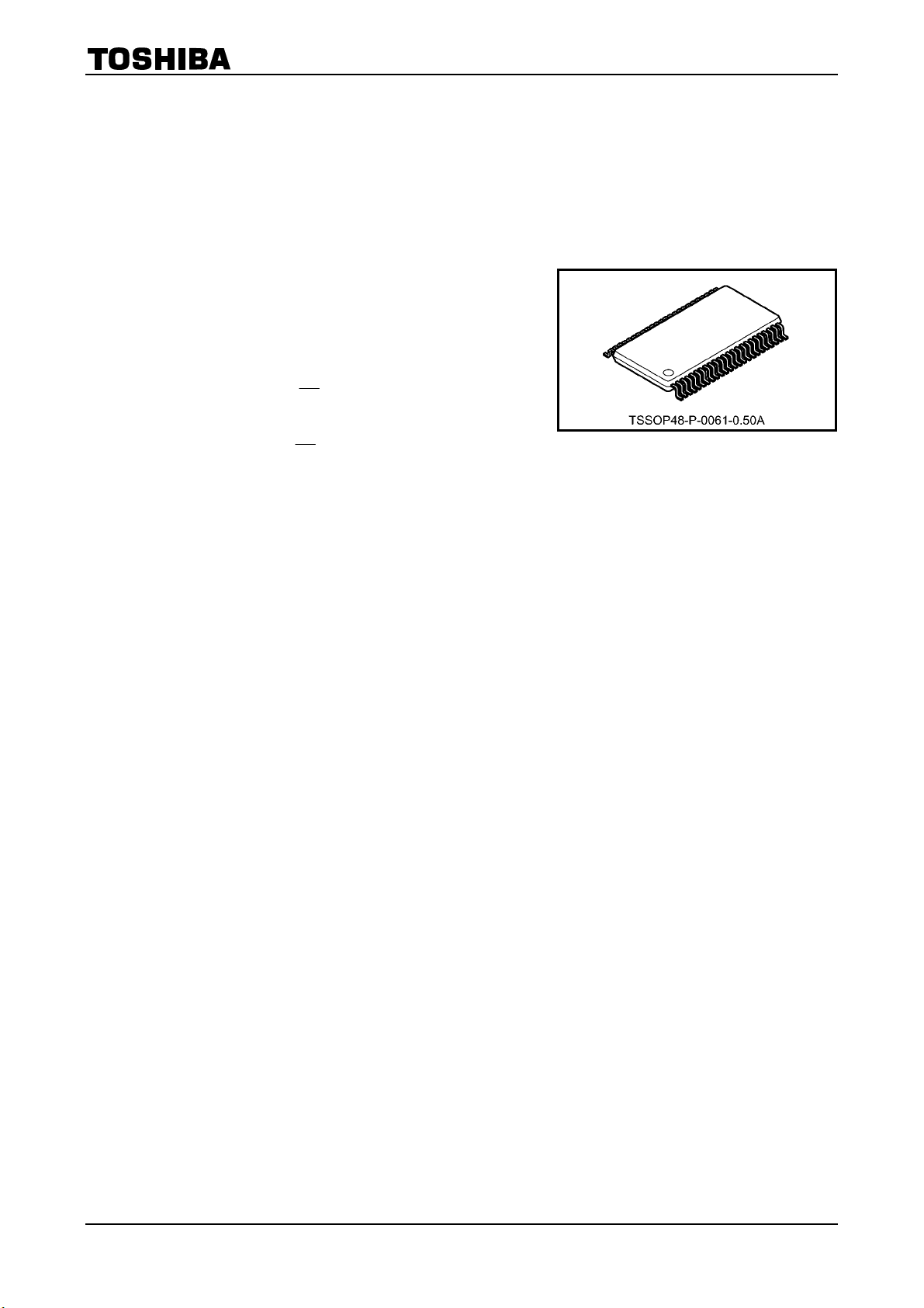
Weight: 0.25 g (typ.)
• 26-Ω series resistors on all outputs
• Low-voltage operation: V
• High-speed operation: t
: tpd = 4.3 ns (max) (VCC = 2.3 to 2.7 V)
: t
• output current: I
: IOH/IOL = ±8 mA (min) (VCC = 2.3 V)
: I
• Latch-up performance: −300 mA
• ESD performance: Machine model ≥ ±200 V
Human body model ≥ ±2000 V
• Package: TSSOP
• Bidirectional interface between 2.5 V and 3.3 V signals.
• 3.6-V tolerant function and power-down protection is provided on all inputs and outputs
Note: Do not apply a signal to any bus pins when it is in the output mode. Damage may result.
All floating (high impedance) bus pins must have their input level fixed by means of pull-up or pull-down
resistors.
OH/IOL
OH/IOL
= 1.8 to 3.6 V
CC
= 3.4 ns (max) (VCC = 3.0 to 3.6 V)
pd
= 5.7 ns (max) (VCC = 1.8 V)
pd
= ±12 mA (min) (VCC = 3.0 V)
= ±4 mA (min) (VCC = 1.8 V)
1
2007-10-19

TC74VCXR162245FT
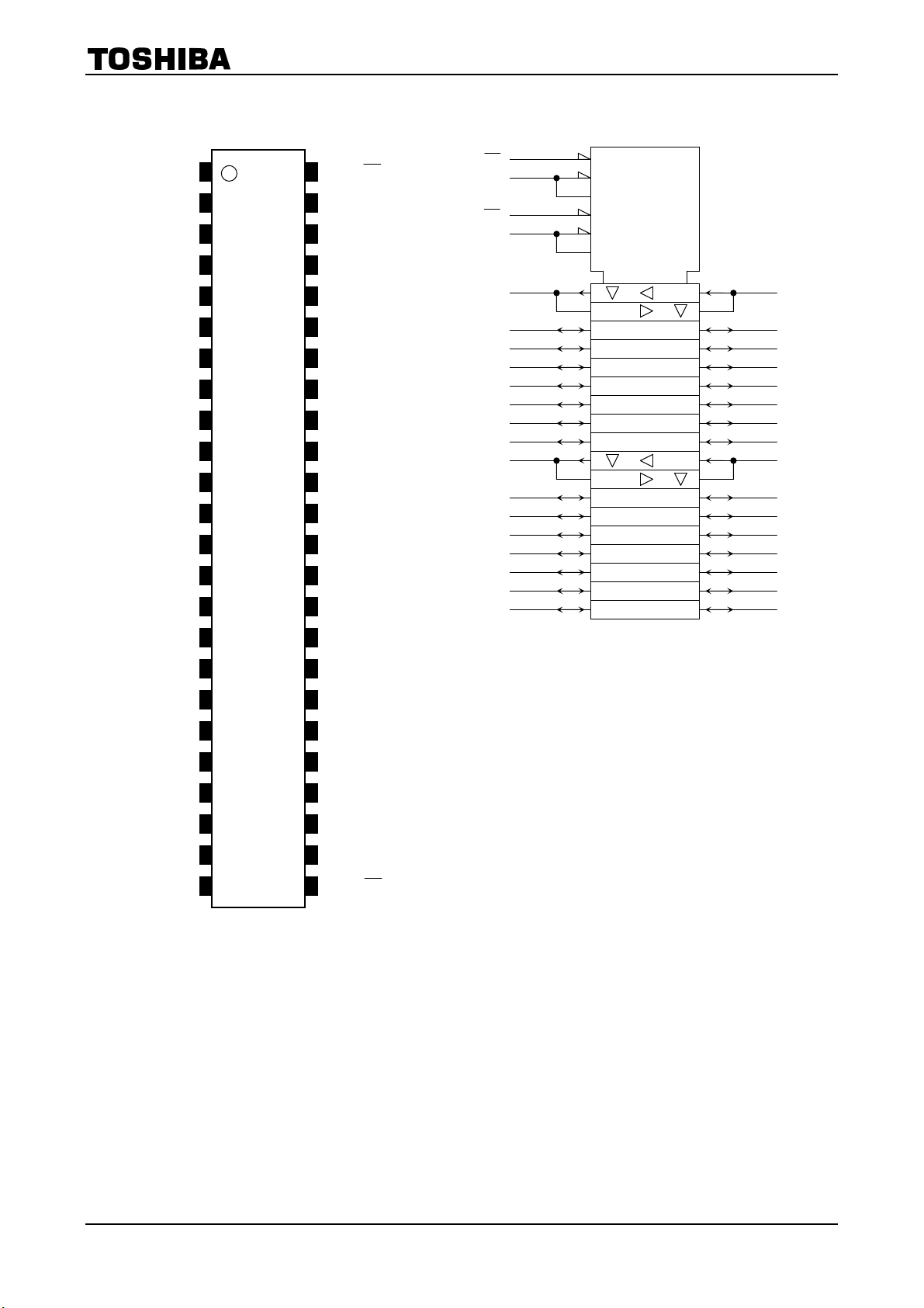
Pin Assignment
1DIR 1
1B1
2
1B2
3
GND
4
5
1B3
1B4
6
V
7
CC
1B5
8
1B6
9
GND
10
11
1B7
1B8
12
13
2B1
14
2B2
GND
15
(top view)
IEC Logic Symbol
47
46
45
44
43
42
41
40
39
38
37
36
35
34
OE148
1A1
1A2
GND
1A3
1A4
V
CC
1A5
1A6
GND
1A7
1A8
2A1
2A2
GND
OE1
1DIR
OE2
2DIR
1A1
1A2
1A3
1A4
1A5
1A6
1A7
1A8
2A1
2A2
2A3
2A4
2A5
2A6
2A7
2A8
48
1
25
24
47
46
44
43
41
40
38
37
36
35
33
32
30
29
27
26
G3
3 EN1 (BA)
3 EN2 (AB)
G6
6 EN4 (BA)
6 EN5 (AB)
1
2
4
2
1B1
3
1B2
5
1B3
6
1B4
8
1B5
9
1B6
11
1B7
12
1B8
13
2B1
5
14
16
17
19
20
22
23
2B2
2B3
2B4
2B5
2B6
2B7
2B8
2B3
2B4
V
CC
2B5
2B6
2B7
2B8
2DIR
16
17
18
19
20
22
23
24
33
32
31
30
29
28 21 GND
27
26
25
2A3
2A4
V
CC
2A5
2A6
GND
2A7
2A8
OE2
2
2007-10-19

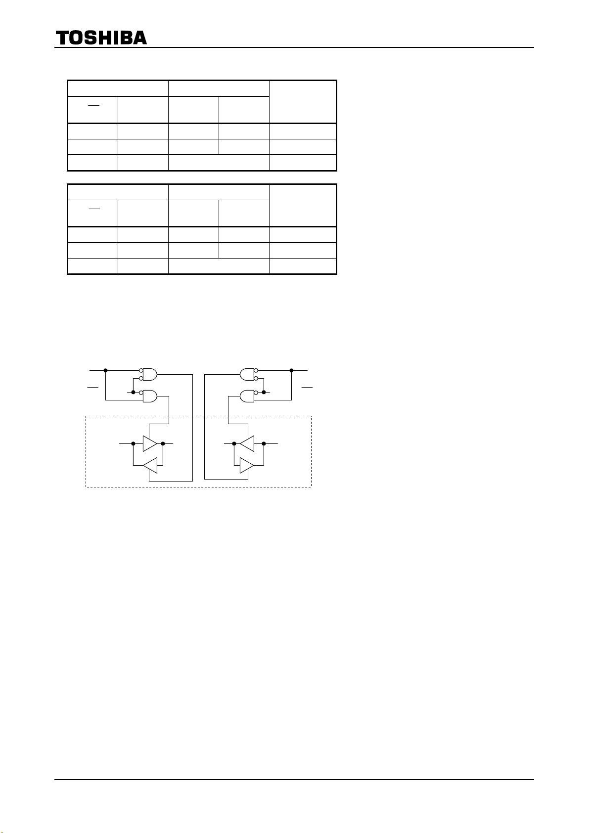
Truth Table
Inputs Function
OE1 1DIR
L L Output Input A = B
L H Input Output B = A
H X Z Z
Inputs Function
OE2 2DIR
L L Output Input A = B
L H Input Output B = A
H X Z Z
X : Don’t care
Z : High impedance
System Diagram
Bus
1A1-1A8
BUS
2A1-2A8
Bus
1B1-1B8
BUS
2B1-2B8
TC74VCXR162245FT
Outputs
Outputs
1DIR
1
48
OE1
47 2 13
1A1
1B1
2B1
25
36
2A1
1/8
24
2DIR
OE2
3
2007-10-19
 Loading...