

TC74VCX86FT/FK
TOSHIBA CMOS Digital Integrated Circuit Silicon Monolithic
TC74VCX86FT,TC74VCX86FK
Low-Voltage Quad 2-Input Exclusive OR Gate with 3.6-V Tolerant Inputs and Outputs
The TC74VCX86FT/FK is a high- performance CMOS exclusive
OR gate which is guaranteed to operate from 1.2-V to 3.6-V.
Designed for use in 1.5V, 1.8V, 2.5V or 3.3V systems, it achieves
high-speed operation while maintaining the CMOS low power
dissipation.
It is also designed with overvoltage tolerant inputs and outputs
up to 3.6 V.
All inputs are equipped with protection circuits against static
discharge.
Features
• Low-voltage operation: VCC = 1.2~3.6 V
• High-speed operation : t
: t
: tpd = 7.8 ns (max) (VCC = 1.65~1.95 V)
: t
: t
• Output current : IOH/IOL = ±24 mA (min) (VCC = 3.0 V)
: I
: I
: IOH/IOL = ±2 mA (min) (VCC = 1.4 V)
• Latch-up performance: −300 mA
• ESD performance: Machine model ≥ ±200 V
Human body model ≥ ±2000 V
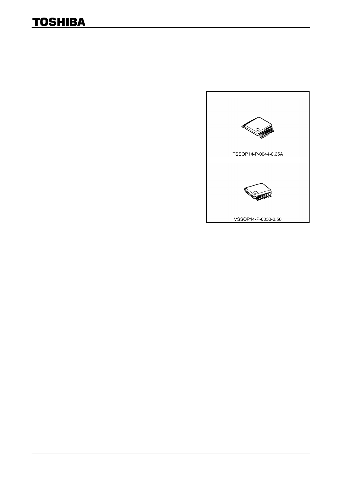
• Package: TSSOP and VSSOP (US)
• Power-down protection provided on all inputs and outputs
OH/IOL
OH/IOL
= 3.0 ns (max) (VCC = 3.0~3.6 V)
pd
= 3.9 ns (max) (VCC = 2.3~2.7 V)
pd
= 15.6 ns (max) (VCC = 1.4~1.6 V)
pd
= 39.0 ns (max) (VCC = 1.2 V)
pd
= ±18 mA (min) (VCC = 2.3 V)
= ±6 mA (min) (VCC = 1.65 V)
TC74VCX86FT
TC74VCX86FK
Weight
TSSOP14-P-0044-0.65A : 0.06g (typ.)
VSSOP14-P-0030-0.50 : 0.02 g (typ.)
1
2007-10-19
TC74VCX86FT/FK
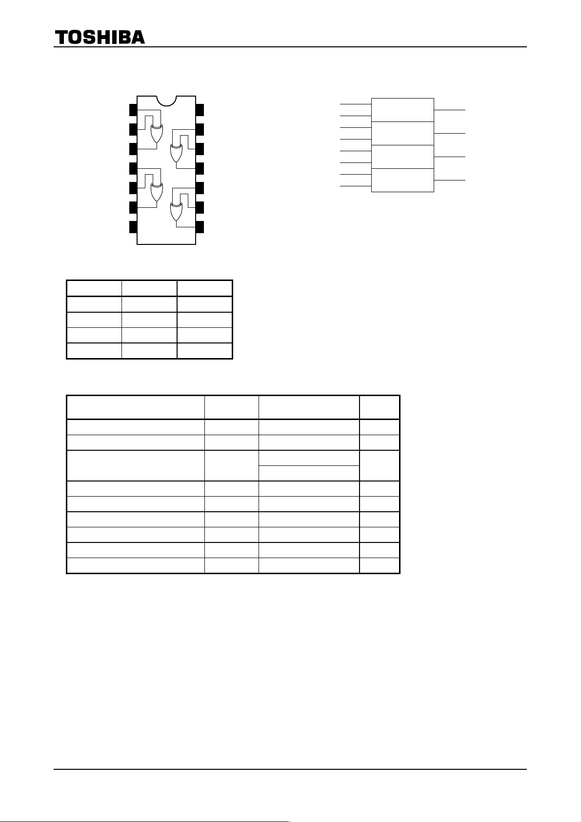
Pin Assignment
(top view)
IEC Logic Symbol
1A 1
1B
1Y
2A
2B
2Y
GND
2
3
4
5
6
7
14
13
12
11
10
9
8
V
4B
4A
4Y
3B
3A
3Y
CC
Truth Table
A B Y
L L L
L H H
H L H
H H L
Absolute Maximum Ratings (Note 1)
1A
1B
2A
2B
3A
3B
4A
4B
(1)
(2)
(4)
(5)
(9)
(10)
(12)
(13)
= 1
(3)
1Y
(6)
2Y
(8)
3Y
(11)
4Y
Characteristics Symbol Rating Unit
Power supply voltage V
DC input voltage V
DC output voltage V
Input diode current I
Output diode current I
DC output current I
Power dissipation P
DC VCC/ground current ICC/I
Storage temperature T
CC
IN
OUT
IK
OK
OUT
D
GND
stg
−0.5~4.6 (Note 2)
±50 (Note 4) mA
−0.5~4.6 V
−0.5~4.6 V
V
−0.5~VCC + 0.5(Note 3)
−50 mA
±50 mA
180 mW
±100 mA
−65~150 °C
Note 1: Exceeding any of the absolute maximum ratings, even briefly, lead to deterioration in IC performance or
even destruction.
Using continuously under heavy loads (e.g. the application of high temperature/current/voltage and the
significant change in temperature, etc.) may cause this product to decrease in the reliability significantly
even if the operating conditions (i.e. operating temperature/current/voltage, etc.) are within the absolute
maximum ratings and the operating ranges.
Please design the appropriate reliability upon reviewing the Toshiba Semiconductor Reliability Handbook
(“Handling Precautions”/“Derating Concept and Methods”) and individual reliability data (i.e. reliability test
report and estimated failure rate, etc).
Note 2: V
Note 3: High or low state. I
Note 4: V
CC
OUT
= 0 V
< GND, V
absolute maximum rating must be observed.
OUT
> VCC
OUT
2
2007-10-19
Operating Ranges (Note 1)
<
<
<
Characteristics Symbol Rating Unit
TC74VCX86FT/FK
Power supply voltage V
Input voltage V
Output voltage V
Output current IOH/IOL
Operating temperature T
Input rise and fall time dt/dv 0~10 (Note 8) ns/V
CC
IN
OUT
opr
0~3.6 (Note 2)
0~VCC (Note 3)
±24 (Note 4)
±18 (Note 5)
±6 (Note 6)
±2 (Note 7)
1.2~3.6 V
−0.3~3.6 V
V
mA
−40~85 °C
Note 1: The operating ranges must be maintained to ensure the normal operation of the device.
Unused inputs must be tied to either VCC or GND.
Note 2: V
CC
= 0 V
Note 3: High or low state
Note 4: VCC = 3.0~3.6 V
Note 5: VCC = 2.3~2.7 V
Note 6: VCC = 1.65~1.95 V
Note 7: VCC = 1.4~1.6 V
Note 8: VIN = 0.8~2.0 V, VCC = 3.0 V
Electrical Characteristics
DC Characteristics
Characteristics Symbol Test Condition
Input voltage
Output voltage
Input leakage current I
Power off leakage current I
Quiescent supply current ICC
Increase in ICC per input ΔICC VIH = VCC − 0.6 V 2.7~3.6 ⎯ 750
(Ta = −40 to 85°C, 2.7 V < V
“H” level
“L” level V
“H” level
“L” level VOL VIN = VIH or VIL
VIH ⎯ 2.7~3.6 2.0 ⎯
⎯ 2.7~3.6 ⎯ 0.8
IL
V
V
OH
IN
OFF
= VIH or VIL
IN
VIN = 0 to 3.6 V 2.7~3.6 ⎯ ±5.0 μA
VIN, V
VIN = VCC or GND 2.7~3.6 ⎯ 20.0
V
CC
= 0 to 3.6 V 0 ⎯ 10.0 μA
OUT
V
3.6 V 2.7~3.6 ⎯ ±20.0
IN
CC
IOH = −100 μA 2.7~3.6
IOH = −12 mA 2.7 2.2 ⎯
IOH = −18 mA 3.0 2.4 ⎯
I
OH
IOL = 100 μA 2.7~3.6 ⎯ 0.2
IOL = 12 mA 2.7 ⎯ 0.4
IOL = 18 mA 3.0 ⎯ 0.4
I
OL
3.6 V)
Min Max Unit
(V)
V
CC
V
CC
− 0.2
= −24 mA 3.0 2.2 ⎯
= 24 mA 3.0 ⎯ 0.55
V
⎯
V
μA
3
2007-10-19

TC74VCX86FT/FK
<
<
<
<
<
<
<
DC Characteristics
Characteristics Symbol Test Condition
Input voltage
Output voltage
Input leakage current I
Power-off leakage current I
Quiescent supply current ICC
(Ta = −40 to 85°C, 2.3 V
H-level
L-level V
H-level
L-level VOL VIN = VIH or VIL
DC Characteristics
(Ta = −40 to 85°C, 1.65 V
V
CC
VIH ⎯ 2.3~2.7 1.6 ⎯
⎯ 2.3~2.7 ⎯ 0.7
IL
IOH = −100 μA 2.3~2.7
V
V
OH
IN
OFF
= VIH or VIL
IN
VIN = 0 to 3.6 V 2.3~2.7 ⎯ ±5.0 μA
VIN, V
VIN = VCC or GND 2.3~2.7 ⎯ 20.0
V
CC
= 0 to 3.6 V 0 ⎯ 10.0 μA
OUT
V
3.6 V 2.3~2.7 ⎯ ±20.0
IN
IOH = −6 mA 2.3 2.0 ⎯
IOH = −12 mA 2.3 1.8 ⎯
I
OH
IOL = 100 μA 2.3~2.7 ⎯ 0.2
IOL = 12 mA 2.3 ⎯ 0.4
I
OL
VCC < 2.3 V)
2.7 V)
Min Max Unit
(V)
V
CC
V
CC
− 0.2
= −18 mA 2.3 1.7 ⎯
= 18 mA 2.3 ⎯ 0.6
V
⎯
V
μA
Characteristics Symbol Test Condition
H-level
Input voltage
L-level V
H-level
Output voltage
L-level VOL VIN = VIH or VIL
Input leakage current I
Power-off leakage current I
Quiescent supply current ICC
Min Max Unit
(V)
V
CC
0.65
×
CC
0.2
V
⎯
CC
⎯
×
μA
VIH ⎯ 1.65~2.3
⎯ 1.65~2.3 ⎯
IL
V
V
OH
IN
OFF
= VIH or VIL
IN
VIN = 0 to 3.6 V 1.65~2.3 ⎯ ±5.0 μA
VIN, V
VIN = VCC or GND 1.65~2.3 ⎯ 20.0
V
CC
= 0 to 3.6 V 0 ⎯ 10.0 μA
OUT
V
3.6 V 1.65~2.3 ⎯ ±20.0
IN
IOH = −100 μA 1.65~2.3
I
= −6 mA 1.65 1.25 ⎯
OH
IOL = 100 μA 1.65~2.3 ⎯ 0.2
= 6 mA 1.65 ⎯ 0.3
I
OL
VCC
V
− 0.2
V
V
4
2007-10-19

<
<
<
<
<
<
DC Characteristics
Characteristics Symbol Test Condition
Input voltage
Output voltage
Input leakage current I
Power-off leakage current I
Quiescent supply current ICC
(Ta = −40 to 85°C, 1.4 V
H-level
L-level V
H-level
L-level VOL VIN = VIH or VIL
DC Characteristics
(Ta = −40 to 85°C, 1.2 V
TC74VCX86FT/FK
VCC < 1.65 V)
VIH ⎯ 1.4~1.65
⎯ 1.4~1.65 ⎯
IL
V
V
OH
IN
OFF
= VIH or VIL
IN
VIN = 0 to 3.6 V 1.4~1.65 ⎯ ±5.0 μA
VIN, V
VIN = VCC or GND 1.4~1.65 ⎯ 20.0
V
CC
= 0 to 3.6 V 0 ⎯ 10.0 μA
OUT
V
3.6 V 1.4~1.65 ⎯ ±20.0
IN
IOH = −100 μA 1.4~1.65
= −2 mA 1.4 1.05 ⎯
I
OH
IOL = 100 μA 1.4~1.65 ⎯ 0.05
I
= 2 mA 1.4 ⎯ 0.35
OL
VCC < 1.4 V)
Min Max Unit
(V)
V
CC
0.65
×
CC
0.2
V
⎯
CC
⎯
×
μA
VCC
V
− 0.2
V
V
Characteristics Symbol Test Condition
H-level
Input voltage
L-level V
H-level
Output voltage
Input leakage current I
Power-off leakage current I
Quiescent supply current ICC
L-level VOL VIN = VIH or VIL I
Min Max Unit
(V)
V
CC
0.8
×
CC
⎯
0.05
V
⎯
CC
×
μA
VIH ⎯ 1.2~1.4
⎯ 1.2~1.4 ⎯
IL
V
V
OH
IN
OFF
= VIH or VIL I
IN
VIN = 0 to 3.6 V 1.2 ⎯ ±5.0 μA
VIN, V
VIN = VCC or GND 1.2 ⎯ 20.0
V
CC
= 0 to 3.6 V 0 ⎯ 10.0 μA
OUT
V
3.6 V 1.2 ⎯ ±20.0
IN
= −100 μA 1.2
OH
= 100 μA 1.2 ⎯ 0.05
OL
VCC
V
− 0.1
V
V
5
2007-10-19

TC74VCX86FT/FK
AC Characteristics
Characteristics Symbol Test Condition
Propagation delay time
(Ta = −40 to 85°C, input: tr = tf = 2.0 ns) (Note)
CL = 15 pF, RL = 2 kΩ
t
pLH
Figure 1, Figure 2
t
pHL
CL = 30 pF, RL = 500 Ω
Note: For CL = 50 pF, add approximately 300 ps to the AC maximum specification.
Dynamic Switching Characteristics
Characteristics Symbol Test Condition
Quiet output maximum dynamic V
Quiet output minimum dynamic VOL V
Quiet output minimum dynamic VOH V
OL
V
OLP
OLV
OHV
(Ta = 25°C, input: tr = tf = 2.0 ns, CL = 30 pF)
VIH = 1.8 V, VIL = 0 V (Note) 1.8 0.25
VIH = 2.5 V, VIL = 0 V (Note) 2.5 0.6
= 3.3 V, VIL = 0 V (Note) 3.3 0.8
V
IH
VIH = 1.8 V, VIL = 0 V (Note) 1.8 −0.25
VIH = 2.5 V, VIL = 0 V (Note) 2.5 −0.6
= 3.3 V, VIL = 0 V (Note) 3.3 −0.8
V
IH
VIH = 1.8 V, VIL = 0 V (Note) 1.8 1.5
VIH = 2.5 V, VIL = 0 V (Note) 2.5 1.9
= 3.3 V, VIL = 0 V (Note) 3.3 2.2
V
IH
V
CC
1.2 1.5 39.0
1.5 ± 0.1 1.0 15.6
1.8 ± 0.15 1.5 7.8
2.5 ± 0.2 0.8 3.9
3.3 ± 0.3 0.6 3.0
Min Max Unit
(V)
(V)
V
CC
Typ. Unit
ns
V
V
V
Note: Parameter guaranteed by design.
Capacitive Characteristics
Characteristics Symbol Test Condition
Input capacitance
Power dissipation capacitance CPD fIN = 10 MHz (Note) 1.8, 2.5, 3.3 20 pF
(Ta = 25°C)
(V)
V
CC
CIN ⎯ 1.8, 2.5, 3.3 6 pF
Typ. Unit
Note: CPD is defined as the value of the internal equivalent capacitance which is calculated from the operating
current consumption without load.
Average operating current can be obtained by the equation:
I
CC (opr)
= CPD・VCC・fIN + ICC/4 (per gate)
6
2007-10-19

AC Test Circuit
TC74VCX86FT/FK
AC Waveform
Output
L
C
Symbol
R
500 Ω 2 kΩ
L
C
L
3.3 ± 0.3 V
2.5 ± 0.2 V
1.8 ± 0.15 V
30 pF 15 pF
L
R
VCC
Measure
Figure 1
1.5 ± 0.1 V
1.2V
tf 2.0 ns tr 2.0 ns
V
Input
(A)
Output
(Y)
Symbol
3.3 ± 0.3 V 2.5 ± 0.2 V 1.8 ± 0.15 V 1.5 ± 0.1 V 1.2 V
VIH 2.7 V VCC V
VM 1.5 V VCC/2 VCC/2 VCC/2 VCC/2
t
pLH
10%
Figure 2 t
90%
VM
V
M
t
pHL
V
CC
V
CC
, t
pHL
pLH
CC
IH
V
OH
VOL
V
CC
7
2007-10-19

Package Dimensions
TC74VCX86FT/FK
Weight: 0.06g (typ.)
8
2007-10-19

Package Dimensions
TC74VCX86FT/FK
Weight: 0.02 g (typ.)
9
2007-10-19

TC74VCX86FT/FK
RESTRICTIONS ON PRODUCT USE
• The information contained herein is subject to change without notice.
• TOSHIBA is continually working to improve the quality and reliability of its products. Nevertheless, semiconductor
devices in general can malfunction or fail due to their inherent electrical sensitivity and vulnerability to physical
stress. It is the responsibility of the buyer, when utilizing TOSHIBA products, to comply with the standards of
safety in making a safe design for the entire system, and to avoid situations in which a malfunction or failure of
such TOSHIBA products could cause loss of human life, bodily injury or damage to property.
In developing your designs, please ensure that TOSHIBA products are used within specified operating ranges as
set forth in the most recent TOSHIBA products specifications. Also, please keep in mind the precautions and
conditions set forth in the “Handling Guide for Semiconductor Devices,” or “TOSHIBA Semiconductor Reliability
Handbook” etc.
• The TOSHIBA products listed in this document are intended for usage in general electronics applications
(computer, personal equipment, office equipment, measuring equipment, industrial robotics, domestic appliances,
etc.).These TOSHIBA products are neither intended nor warranted for usage in equipment that requires
extraordinarily high quality and/or reliability or a malfunction or failure of which may cause loss of human life or
bodily injury (“Unintended Usage”). Unintended Usage include atomic energy control instruments, airplane or
spaceship instruments, transportation instruments, traffic signal instruments, combustion control instruments,
medical instruments, all types of safety devices, etc.. Unintended Usage of TOSHIBA products listed in his
document shall be made at the customer’s own risk.
• The products described in this document shall not be used or embedded to any downstream products of which
manufacture, use and/or sale are prohibited under any applicable laws and regulations.
• The information contained herein is presented only as a guide for the applications of our products. No
responsibility is assumed by TOSHIBA for any infringements of patents or other rights of the third parties which
may result from its use. No license is granted by implication or otherwise under any patents or other rights of
TOSHIBA or the third parties.
20070701-EN GENERAL
• Please contact your sales representative for product-by-product details in this document regarding RoHS
compatibility. Please use these products in this document in compliance with all applicable laws and regulations
that regulate the inclusion or use of controlled substances. Toshiba assumes no liability for damage or losses
occurring as a result of noncompliance with applicable laws and regulations.
10
2007-10-19
 Loading...